

Page 1
ADJUSTABLE PRECISION
V
Z
G
nd
V
ref
ZENER SHUNT REGULATOR
ISSUE 2 – FEBRUARY 1997
ZHT431
DEVICE DESCRIPTION
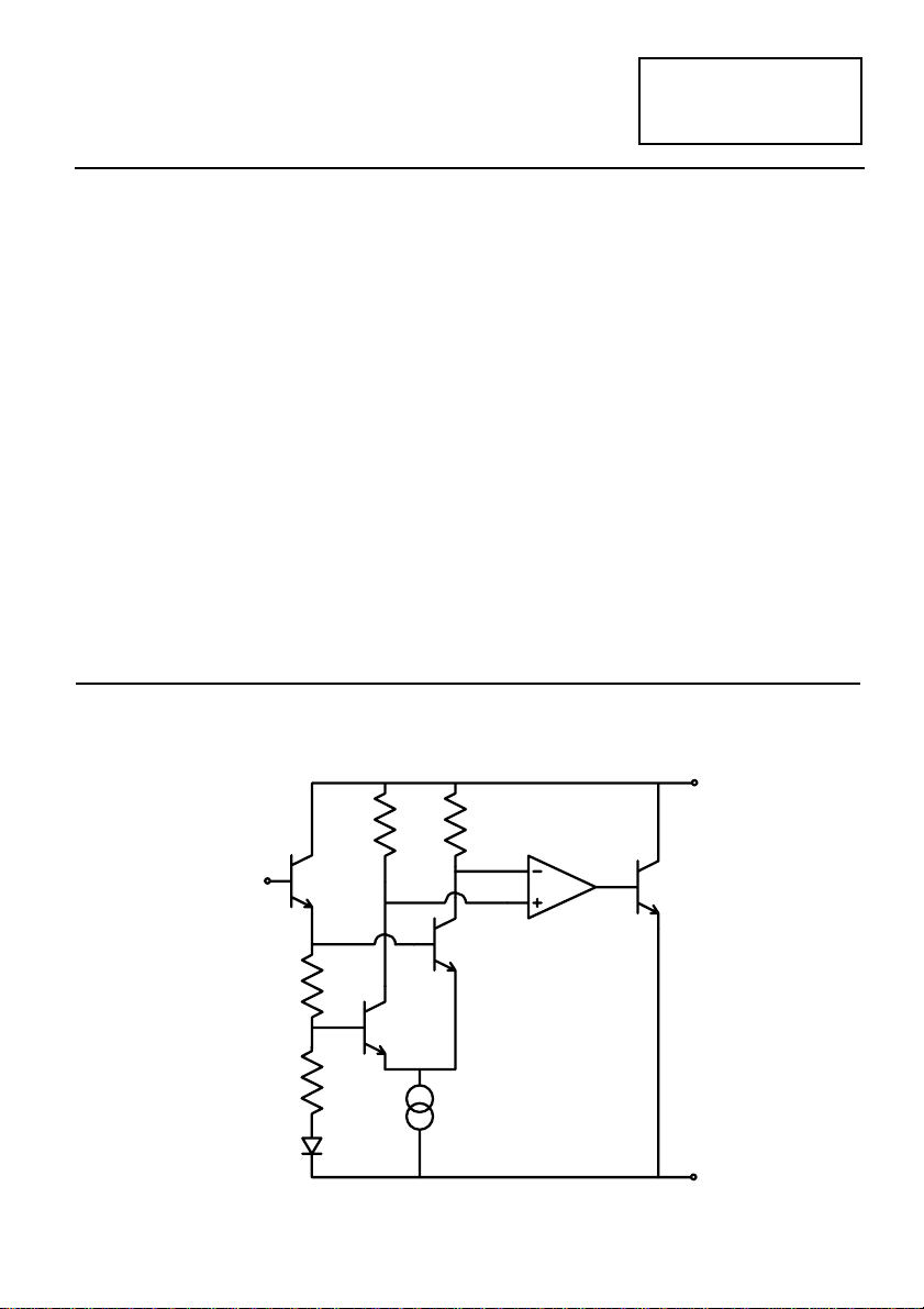
The ZHT431 is a three terminal adjustable
shunt regulator offering excellent
temperature stability and output current
handling capability up to 100mA. The device
offers extended operating temperature
range working from -55 to +125°C. The
output voltage may be set to any chosen
voltage between 2.5 and 20 volts by
selection of two external divider resistors.
The devices can be used as a replacement
for zener diodes in many applications
requiring an improvement in zener
performance.
SCHEMATIC DIAGRAM
FEATURES
Surface mount SO8, SOT89, SOT223
•
and SOT23 packages
TO92 package
•
2% and 1% tolerance
•
Maximum temperature coefficient 67
•
ppm/°C
Temperature compensated for
•
operation over the full temperature
range
Programmable output voltage
•
50µA to 100mA current sink capability
•
Low output noise
•
Wide temperature range -55 to +125°C
•
APPLICATIONS
Series and Shunt regulator
•
Voltage monitor
•
Over voltage/ under voltage protection
•
Switch mode power supplies
•
4-28
Page 2

ABSOLUTE MAXIMUM RATING
Cathode Voltage (VZ) 20V
Cathode Current 150mA
Operating Temperature -55 to 125°C
Storage Temperature -55 to 150°C
Recommended Operating Conditions
Min Max
Cathode Voltage Vref 20V
Cathode Current 50µA 100mA
ZHT431
Power Dissipation (T
(T
= 150°C)
jmax
SOT23 330mW
TO92 780mW
SOT223 2W
SO8 780mW
SOT89 1.5W
amb
=25°C)
ELECTRICAL CHARACTERISTICS TEST CONDITIONS (Unless otherwise stated):T
PARAMETER
Reference Voltage 2%
SYMBOL
V
ref
1%
Deviation of Reference Input
V
dev
Voltage over Temperature
Ratio of the change in
Reference Voltage to the
∆
V
∆
Change in Cathode
Voltage
Reference Input Current I
Deviation of Reference Input
ref
∆
I
Current over Temperature
Minimum Cathode
I
Zmin
Current for Regulation
Off-state Current I
Dynamic Output
R
Zoff
Z
Impedance
Deviation of reference input voltage, V
input voltage over the full temperature range.
The average temperature coefficient of the reference input voltage, V
Vmax
Vmin
Vdev = Vmax - Vmin
T1 T2
Temperature
VALUE
MIN TYP MAX
2.45
2.475
ref
V
Z
ref
dev,
UNITS CONDITIONS
2.50
2.55
2.50
VI
2.525
=10mA (Fig1), VZ=V
L
10 30 mV IL=10mA, VZ=V
Ta=full range (Fig1)
-1.85 -2.7 mV/V VZ from V
I
=10mA (Fig2)
Z
-1.0 -2.0 mV/V V
0.12 1.0
µA
from 10V to 20V
Z
I
=10mA (Fig2)
Z
R1=10k, R2=O/C, lL=10mA
to 10V
ref
(Fig2)
0.04 0.2
35 50
0.1
0.75
µA
µA
µA
Ω
R1=10k, R2=O/C, IL=10mA
T
=full range (Fig2)
a
VZ=V
(Fig1)
ref
VZ=20V, V
VZ=V
I
=1mA to 100mA
C
=0V(Fig3) †
ref
(Fig1), f=0Hz,
ref
is defined as the maximum variation of the reference
is defined as:
ref
V
x 1000000
dev
V
(
ppm
⁄
ref
°C)=
V
ref
(T1−T2)
The dynamic output impedance, Rz, is defined as:
V
∆
Z
R
=
Z
∆
I
Z
When the device is programmed with two external
resistors, R1 and R2, (fig 2) , the dynamic output
impedance of the overall circuit, R’, is defined as:
R
R’=R
(1+
z
1
)
R
2
ref
amb
=25°C
ref
4-29
Page 3
ZHT431
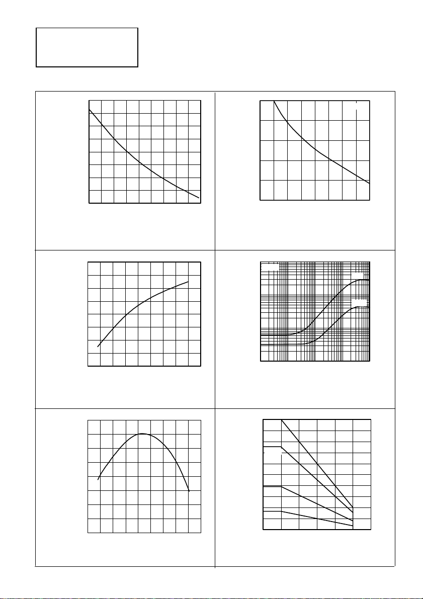
170
160
150
140
130
120
110
Reference Current (nA)
100
90
-50 -25 0 25 50 75 100 125
I
TYPICAL CHARACTERISTICS
Temperature ( °C)
ref
vs. Temperature
Change in Reference Output Voltage (mV)
0
-5
-10
-15
-20
-25
0
Change in V
IZ=10mA
5101520
Cathode Voltage (V)
r
ef
v Cathode Voltage
40
38
36
34
32
30
28
26
Minimum Cathode Current (µA)
24
-50 -25 0 25 50 75 100 125
Temperature ( °C)
zmin
I
vs. Temperature
2.502
2.500
2.498
2.496
2.494
2.492
2.490
Reference Voltage (V)
2.488
2.486
-50 -25 0 25 50 75 100 125
Temperature ( °C)
ref
V
vs. Temperature
100
ref=VZ
V
10
1.0
Dynamic Impedance (Ω)
0.1
100 1k 10k 100k 1M
Frequency (Hz)
Dynamic Impedance v Frequency
2.0
1.8
1.6
SOT89
1.4
1.2
1.0
0.8
0.6
0.4
Power Dissipation (W)
0.2
0
0 15050 100 125
SOT223
SO8/
TO92
SOT23
25 75
Ambient Temperature ( °C)
Power Dissipation Derating
1mA
10mA
4-30
Page 4

ZHT431
TYPICAL CHARACTERISTICS
60
Z
I
40
15k
9µF
230
V
Z
20
Open Loop Voltage Gain (dB)
0
100 1k 10k 100k 1M
Frequency (Hz)
Gain v Frequency
3.0
2.0
1.0
0
Voltage Swing (V)
5.0
0
Repetitive pulse
Single pul se
0 0.4 0.6 0.8 1.00.2
Time (µs)
Pulse Response
100
80
60
STABLESTABLE
Z
V
INPUT
+
= 10mA,
IZ
8k25
TA = 25°C
-
Test Circuit for Open Loop Voltage Gain
Input Monitor
Generator
Pulse
TA= 25°C
220
50
Test Circuit for Pulse Response
Input
150
Z
I
10k
V
Z
VZ
40
20
Cathode Current (mA)
0
10p
100p 1000p
Load Capacitance (F)
Stability Boundary Conditions
0.01µ0.1µ1
µ
V
< VZ< 20, IZ= 10mA, TA= 25°C
ref
Test Circuit for Stability Boundary Conditions
4-31
Page 5

ZHT431
DC TEST CIRCUITS
L
I
Input
Input V
I
zoff
Z
Fig 1 – Test Circuit for Vz=V
Fig 2 – Test Circuit for Vz>V
ref
ref
Fig 3 – Test Circuit for Off
State current †
NOTE
† Since the “Off State” disables all internal circuitry including leakage control, operating in this
mode at high temperature is not recommended.
4-32
Page 6

APPLICATION CIRCUITS
V
ZHT431
V+ Vout
R1
Vref
R2
R1
1 +
Vout =
SHUNT REGULATOR
+
ZSR***
In
Common
Vout = Vref + Vreg
MIN
Vout = 1 +
OUTPUT CONTROL OF A
THREE TERMINAL FIXED REGULATOR
Vref
R2
Vout
Out
R1
Vref
R2
R1
Vref
R2
V+ Vout
R1
Vref
R2
30
0.01µF
R1
1 +
Vref
R2
R1
R2
R1
Vref
R2
Vout =
HIGHER CURRENT SHUNT REGULATOR
V+
Vref
Vout = 1 +
SERIES REGULATOR
Vout
V+
INPUT
= 2.5V
V
TH
SINGLE SUPPLY COMPARATOR
WITH TEMPERATURE
COMPENSATED THRESHOLD
OUTPUT
V
V
V+
R1A
2V
on
= V+
off
Vref
R2A
R1B
R2B
R1B
1 +
Low limit =
High limit =
OVER VOLTAGE / UNDER VOLTAGE
Vref
R2B
R1A
1 +
Vref
R2A
PROTECTION CIRCUIT
Vref
OUTPUT
4-33
Page 7

ZHT431
CONNECTION DIAGRAMS
SO8 Package Suffix – N8
SOT223 Package Suffix – G
Top View
SOT23 Package Suffix – F
Top View
ORDERING INFORMATION
PART No TOL
ZHT431N802 2 SO8 ZHT43102
ZHT431N801 1 SO8 ZHT43101
ZHT431G02 2 SOT223 ZHT43102
PACKAGE PARTMARK
%
Top View –
Pin 4 floating or connected to pin 2
TO92 Package Suffix – C
Bottom View
SOT89 Package Suffix – Z
Top View –
Pin 4 floating or connected to pin 2
ZHT431G01 1 SOT223 ZHT43101
ZHT431F02 2 SOT23 43D
ZHT431F01 1 SOT23 43C
ZHT431C02 2 TO92 ZHT43102
ZHT431C01 1 TO92 ZHT43101
ZHT431Z02 2 SOT89 43F
ZHT431Z01 1 SOT89 43E
4-34
 Loading...