

Page 1

DS97KEY0102
P R E L I M I N A R Y
1
1
P
RELIMINARY
P
RODUCT
S
PECIFICATION
Z86U18
1
USB D
EVICE
C
ONTROLLER
WITH
CMOS Z86K15 MCU
FEATURES
■
USB Serial Interface Engine, Transceiver, and MCU
Intergrated for USB Function Controller
■
+4.0V to +5.5V Operating Range
■
Low Power Consumption: 60 mW @ 6 MHz
■
Digital Inputs CMOS Levels with Internal Pull-Up
Resistors
■
Four Direct Connect LED Drive Ports
■
Power-On Reset (POR), Hardware Watch-Dog Timer
(WDT)
■
Intergrated USB Transceiver @ 1.5 Mb/sec
■
For Use In A Variety of Applications Including Keyboards
and Game Controllers
■
Programmable 8-Bit Counter/Timer, with 6-Bit
Programmable Prescaler
■
Five Vectored, Priority Interrupts from Five Different
Sources
■
On-Chip Oscillator, Which Accepts A Crystal, Ceramic
Resonator, LC or External Clock Drive (all clock speeds
@ 6 MHz)
■
Low System EMI Emission
■
HALT/STOP Modes
GENERAL DESCRIPTION
The Z86U18 USB Controller is a member of the Z8
¨
MCU
family. The Z86U18 is characterized by a flexible I/O
scheme, an efficient register architecture, and a number of
ancillary features. It contains a dedicated USB interface
(transceiver and SIE).
For applications demanding powerful I/O capabilities, the
Z86U18 (40- and 44-pin versions) provides 32 pins dedicated to application input and output. These lines are
grouped into four ports, each port consists of eight lines
and are configurable under software control to provide timing, status signals, and serial or parallel I/O ports. It also
has 2 pins to connect directly to the USB cable.
To unburden the system from coping with real-time tasks,
such as counting/timing and I/O data communications, the
Z86U18 offers an on-chip counter/timer with a large number of user-selectable modes.
The Z86U18 achieves low EMI by means of several circuit
implementations in the output drivers and clock circuitry of
the device.
With fast execution, efficient use of memory, sophisticated
interrupt, input/output bit-manipulation capabilities, and
easy hardware/software system expansion, along with low
cost and low power consumption, the Z86U18 meets the
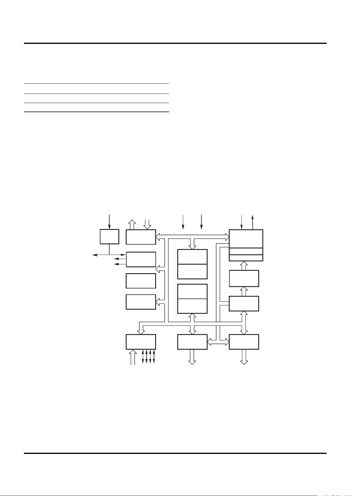
needs of a variety of sophisticated applications (Figure 1:
Functional Block Diagram)
Notes : All signals with a preceding front slash, "/", are ac-
tive Low. For example, B//W (WORD is active Low); /B/W
(BYTE is active Low, only).
Device
ROM
(KB)
RAM
(Bytes)
I/O
Lines
Speed
(MHz)
Z86U18 4 188 32 6
Page 2
Z86U18
USB Device Controller with CMOS Z86K15 MCU Zilog
2
P R E L I M I N A R Y
DS97KEY0102
GENERAL DESCRIPTION (Continued)
Power connections follow conventional descriptions below:
This device is based on the Z86K15 device with the following changes or modifications:
1.
Power-On Reset (POR): POR timing is a function of
the system clock.
POR = (3
2
* 2
16
)/f = .098
POR is in seconds and frequency in Hz. It may need
a programmable timer for warm reset (USB reset).
2.
Watch-Dog Timer (WDT): WDT is also driven by the
system clock and subject to same tolerance. The
WDT can be programmed for time out value of:
WDT = POR/2
3. EMI, 801-2 and 801-4 Compliance : When used with
good engineering practice, this device should meet
Class B FCC with at least 10 dB of margin and comply
with the 801-2 group 4 air discharge. It shall meet 8014 EFT requirements in a system.
4. XTAL : Drive to 3-pin ceramic resonator (@ 6 MHz).
5.
XTAL In : From ceramic resonator or crystal.
Connection Circuit Device
Power V
CC
V
DD
Ground GND V
SS
Figure 1. Z86U18 Functional Block Diagram
Port 3
Interrupt
Control
Port 2
I/O
(Bit Programmable)
ALU
Flags
Register
Pointer
Machine
Timing & Inst.
Control
Program
Counter
GND
XTAL1
XTAL2
Output
Input
Port 0 Port 1
Open-Drain
Output
Open-Drain
Output
WDT
POR
Input
4
4
4
8 8
Counter/
Timers
USB SIE
and Trans
Register File
208 x 8-Bytes
Program
Memory
4 KB ROM
VCC
D+
D-
3.3 V
VR
VCC
V
USB
Page 3
Z86U18
Zilog USB Device Controller with CMOS Z86K15 MCU
DS97KEY0102
P R E L I M I N A R Y
3
1
USB FUNCTIONAL BLOCK DESCRIPTION
The USB portion of the chip is divided into two areas, the
transceiver and the Serial Interface Engine (SIE). The
transceiver handles incoming differential signals and "single ended zero" (SE0). It also converts output data in digital form to differential drive at the proper levels.
The SIE does all other processing on incoming and out going data. This includes signal recovery timing, bit stuffing,
validity checking, data sequencing, and handshaking to
the host. Data flow into and out of the MCU portions is processed through eight registers mapped into Expanded
Register File Memory at locations 010 to 017.
The USB SIE handles two endpoints (control at Endpoint
0 and data into the host from Endpoint 1). All communications are at the 1.5 Mb/sec HID class data rate. Future devices will handle the full 12 Mb/sec data rate.
USB SUSPEND/RESUME FUNCTIONALITY
Suspend is intitiated by the host only, when it stops sending start of frame signaling or start of frame keep alive
pulse.
When SIE detects the absence of start of frame signaling
from the host for more than 3 miliseconds, it sets the Suspend bit in Reg7 and the Supspend Interrupt bit in Reg6
which interrupts the microcontroller. There is also an internal Suspend node that reflects the state of the Suspend bit
in Reg7. This Suspend node is used to put the tranceiver
in Suspend mode. When the microcontroller gets the Suspend Interrupt, it stops all the clocks.
Resume can be initiated by host or by UC. Host initiates
Resume by sending J to K transition on D+ and D- pins.
Upon detecting J to K transition, the GFI makes Resumeout signal active, which is used to wake the UC. Once the
UC is up, it clears the suspend bit in Reg7. UC can initiate
Resume by writing 1 to Send Resume bit in Reg7 for longer than 10mSec. This makes GFI to send J to K transition
on D+ and D- pins which indicates to the host the Resume
state. After 10 msec UC also clears the Suspend bit in
Reg7.
U18 EMULATIONS AND CODE DEVELOPMENT
An existing ICEBOXª Emulator has been modified by the
addition of an adaptor board. This board includes a FPGA
with the logic of the SIE, a commercial USB transceiver,
and a voltage regulator. These three functions adapt our
Z86C15/K15 to the USB world allowing the customer to
develop code to be placed into the ROM of U18s.
The ICEBOX has complete functional equivalence to the
final part including pin out to the application board. This
begins with the 40-pin DIP and covers the other pin configurations. Once code has been verified, it can be released
to Zilog and placed into the ROM of the Z86U18.
Figure 2. Data To/From K86U18
SYNC DATA CRC EOP
Data packet sent at low speed
SYNC
SYNC
Hub Setup
ENDP . . .
EOP
Hub enables low
speed port outputs
Hub enables low
speed port outputs
Preamble
sent at full speed Token sent at low speed
SYNCSYNC Hub Setup EOP
Preamble
sent at full speed
Hub enables low
speed port outputs Handshake sent at low speed
Hub enables low
speed port outputs
PID
PID
PID
PID
PID
Page 4
Z86U18
USB Device Controller with CMOS Z86K15 MCU Zilog
4
P R E L I M I N A R Y
DS97KEY0102
PIN IDENTIFICATION
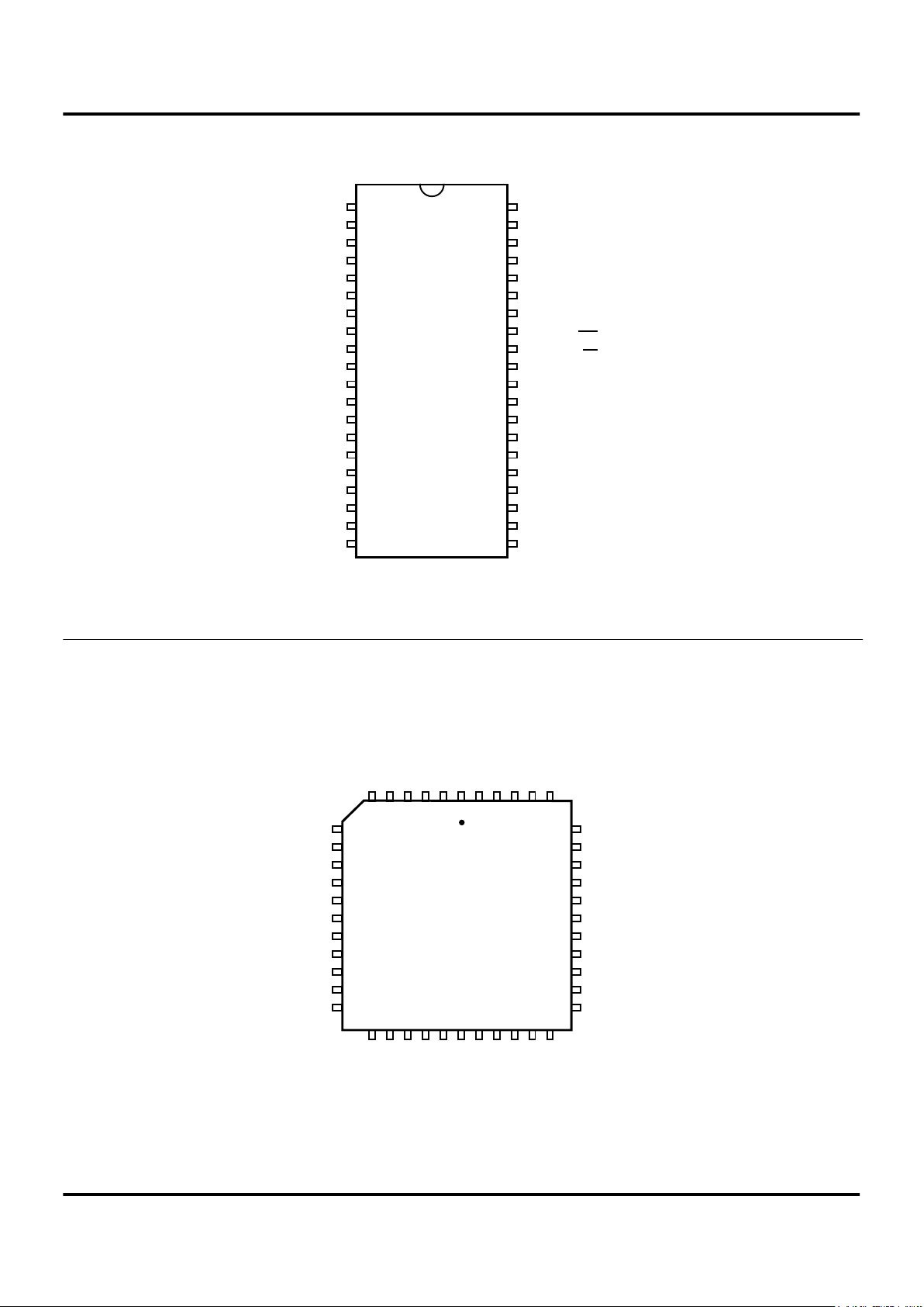
Figure 3. 40-Pin DIP Pin ConÞguration
P36
P17
P16
P15
P14
P13
P12
P11
P10
P35
GND
P00
P01
P02
P03
P04
P05
P06
P07
P34
P23
P22
P21
P20
P37
P24
Test
XTALI (IN)
XTAL0
GND
P25
P26
VUSB
V
CC
D+
DP30
P31
P32
P33
40
Z86UXX
DIP
1
20 21
2
3
4
5
6
7
8
9
10
11
12
13
14
15
16
17
18
19
39
38
37
36
35
34
33
32
31
30
29
28
27
26
25
24
23
22
(OUT)
Pin assignments to be determined.
Figure 4. 44-Pin PLCC and QFP Pin Assignments
Z86U18
PLCC/QFP
7
8
9
10
11
12
13
14
15
16
17
XXX
XXX
XXX
XXX
XXX
XXX
XXX
XXX
XXX
XXX
XXX
XXX
XXX
XXX
XXX
XXX
XXX
XXX
XXX
XXX
XXX
XXX
XXX
XXX
XXX
XXX
XXX
XXX
XXX
XXX
XXX
XXX
XXX
XXX
XXX
XXX
XXX
XXX
XXX
XXX
XXX
XXX
XXX
XXX
1
2818
406
39
38
37
36
35
34
33
32
31
30
29
20 22 24 26
4
42
Page 5
Z86U18
Zilog USB Device Controller with CMOS Z86K15 MCU
DS97KEY0102
P R E L I M I N A R Y
5
1
Pin assignments to be determined.
Figure 5. 28-pin SOIC Assignments
XXX
XXX
XXX
XXX
XXX
XXX
XXX
XXX
XXX
XXX
XXX
XXX
XXX
XXX
XXX
XXX
XXX
XXX
XXX
XXX
XXX
XXX
XXX
XXX
XXX
XXX
XXX
XXX
28
Z86U18
SOIC
1
14 15
Pin assignments to be determined.
Figure 6. 28-pin PDIP Assignments
XXX
XXX
XXX
XXX
XXX
XXX
XXX
XXX
XXX
XXX
XXX
XXX
XXX
XXX
XXX
XXX
XXX
XXX
XXX
XXX
XXX
XXX
XXX
XXX
XXX
XXX
XXX
XXX
28
Z86U18
PDIP
1
14 15
Page 6
Z86U18
USB Device Controller with CMOS Z86K15 MCU Zilog
6
P R E L I M I N A R Y
DS97KEY0102
ABSOLUTE MAXIMUM RATINGS
Stresses greater than those listed under Absolute Maximum Ratings may cause permanent damage to the device. This is a stress rating only; operation of the device at
any condition above those indicated in the operational sections of these specifications is not implied. Exposure to absolute maximum rating conditions for extended periods
may affect device reliability.
STANDARD TEST CONDITIONS
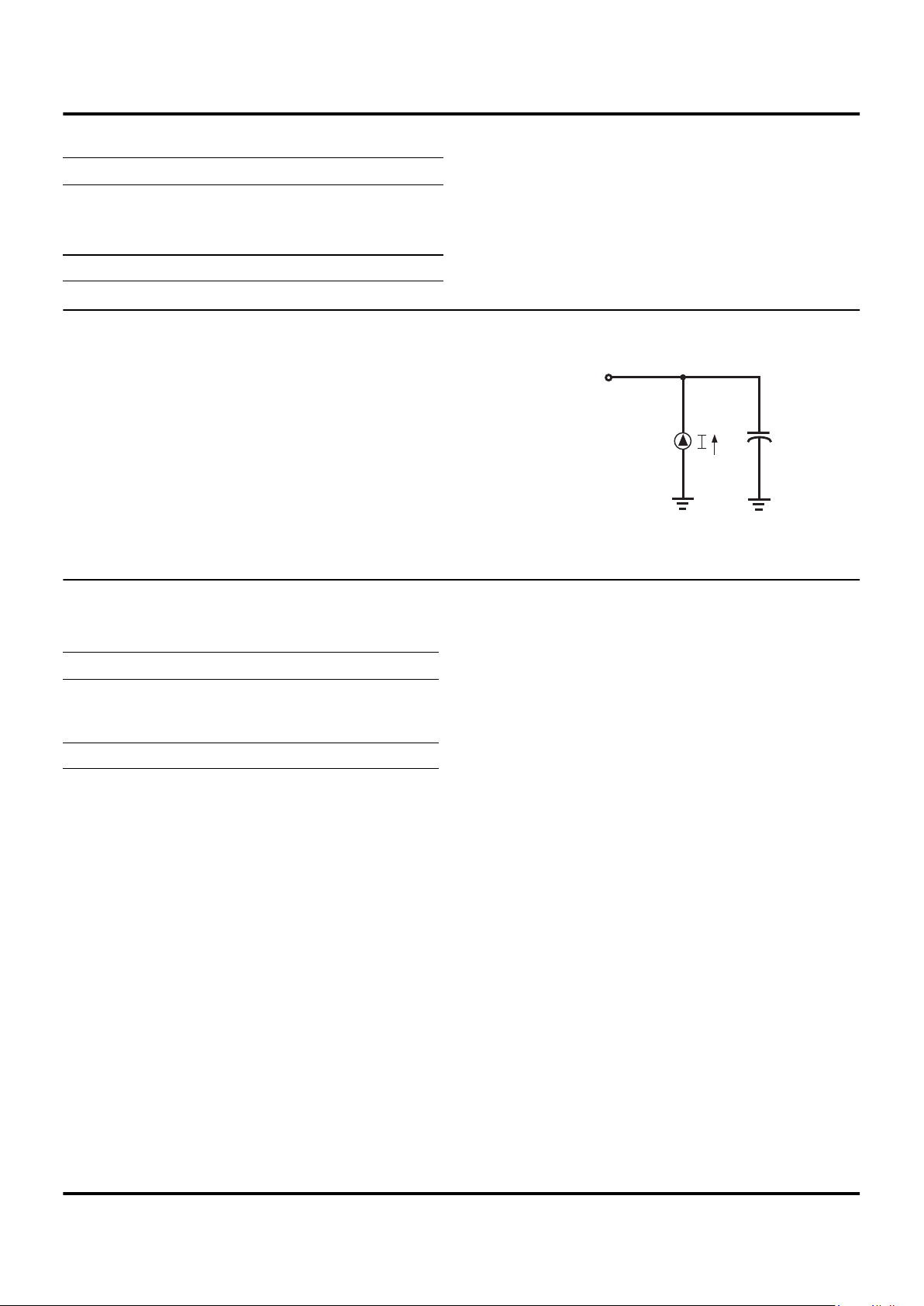
The characteristics listed here apply for standard test conditions as noted. All voltages are referenced to GND. Positive current flows into the referenced pin (Figure 7).
CAPACITANCE
T
A
= 25 ° C; V
CC
= GND = 0V; f = 1.0 MHz; unmeasured pins returned to GND.
Symbol Description Min Max Units
V
CC
Supply Voltage* Ð0.3 +7.0 V
T
STG
Storage Temp Ð65 +150 ° C
T
A
Oper Ambient Temp 0 +105 ° C
Note: * Voltage on all pins with respect to GND.
Figure 7. Test Load Diagram
From Output
Under Test
150 pF
Parameter Max
Input Capacitance 12 pF
Output Capacitance 12 pF
I/O Capacitance 12 pF
Note: Frequency tolerance ± 10%
Page 7

Z86U18
Zilog USB Device Controller with CMOS Z86K15 MCU
DS97KEY0102
P R E L I M I N A R Y
7
1
DC CHARACTERISTICS
V
CC
= 4.0V to 5.5V @ 0 ° C to +70 ° C
Sym Parameter Min Max Unit Condition
V
CH
Clock Input High Voltage 0.7 V
CC
V
CC
+ 0.3V V Driven by External Clock Generator
V
CL
Clock Input Low Voltage GND Ð0.3 0.2 V
CC
V Driven by External Clock Generator
V
IH
Input High Voltage 0.7 V
CC
V
CC
+ 0.3 V
V
IL
Input Low Voltage GND Ð0.3 0.2 V
CC
V
V
OH
Output High Voltage VCC Ð0.4 V IOH = Ð2.0 mA
V
OH
Output High Voltage VCC Ð0.6 V I
OH
= Ð2.0 mA (see note 1 below.)
V
OL
Output Low Voltage .4 V IOL= 4 mA
V
OL
Output Low Voltage .8 V IOL= 4 mA (see note 1 below.)
I
OL
Output Low 10 20 mA VOL= VCC Ð2.2 V (see note 1 below.)
I
OL
Output Leakage Ð1 1 mAVIN = 0V, 5.25V
I
CC
VCC Supply Current 12 mA @ 6.0 MHz
I
CC1
Halt Mode Current TBD mA @ 6.0 MHz
I
CC2
Stop Mode Current 10 mA
R
p
Pull Up Resistor 6.76 14.04 K ohm
R
p
Pull Up Resistor (P26-P25) 1.8 3 K ohm
VUSB Voltage Regulator Output 3.0 3.6 V
D+,D- Differential Signaling D- > D+ D+ > D- mV @ > 200mV Difference (see note 2
below)
Notes:
1. Ports P37-P34. These may be used for LEDs or as general-purpose outputs requiring high sink current.
2. Except for SE0 for EOP and RESET (See 7.1.4 of USB Specification).
Page 8
Z86U18
USB Device Controller with CMOS Z86K15 MCU Zilog
8 P R E L I M I N A R Y DS97KEY0102
AC ELECTRICAL CHARACTERISTICS
Additional Timing Diagram
Figure 8. Additional Timing
Clock
1
3
4
8
223
TIN
IRQN
6
5
7
7
1
1
Clock
Setup
1
0
9
S
top
Mode
Recovery
Source
Page 9

Z86U18
Zilog USB Device Controller with CMOS Z86K15 MCU
DS97KEY0102 P R E L I M I N A R Y 9
1
AC ELECTRICAL CHARACTERISTICS
Additional Timing Table
T
A
=0°C to +70°C
5.0V, 6 MHz
No Symbol Parameter Min Max Units Notes
1 TpC Input Clock Period 150 250 ns 1
2 TrC,TfC Clock Input Rise & Fall Times 25 ns 1
3 TwC Input Clock Width 37 ns 1
4 TwTinL Timer Input Low Width 70 ns 1
5 TwTinH Timer Input High Width 2.5TpC 1
6 TpTin Timer Input Period 4TpC 1
7 TrTin Timer Input Rise & Fall Timer 100 ns 1
8 TwIL Int. Request Low Time 70 ns 1,2
9 TwIH Int. Request Input High Time 3TpC 1,2
10 Twsm Stop-Mode Recovery Width Spec 5TpC ns
11 Tost Oscillator Start-up Time 5TpC ns
12 Twdt Watch-Dog Timer 3,0 ms
13 D+, D- Differential Rise and Fall Times 70 300 nS 3
Notes:
1. Timing Reference uses 0.7 V
CC
for a logic 1 and 0.2 VCC for a logic 0.
2. Interrupt request through Port 3 (P33-P31)
3. See USB Specification 7.1.1.2
Page 10

Z86U18
USB Device Controller with CMOS Z86K15 MCU Zilog
10 P R E L I M I N A R Y DS97KEY0102
PIN FUNCTIONS
XTAL 1,2 for ceramic resonator operation (6 MHz). Port 0 (P07-P00) and Port 1 (P17-P10). Port 0 and Port
1 are 8-bit open drain output (Figure 9).
Figure 9. Port 0 and Port 1 ConÞguration
(Open-Drain
Output)
Z86UXX
8
Pad
Output
Port 0 and Port 1
Page 11
Z86U18
Zilog USB Device Controller with CMOS Z86K15 MCU
DS97KEY0102 P R E L I M I N A R Y 11
1
Port 2 (P27-P20). Port 2 is an 8-bit CMOS-compatible
Port with 4-bit input, 4-bit programmable I/O (Figure 10).
P20-P24 have 10.4 K (±35 percent) pull-up resistors. P25
and P26 have 2.4 K (±25 percent) pull-up resistor.
Figure 10. Port 2 ConÞguration
Open-Drain
OUT
OEN
IN
Pad
2.4K
Input
(c) Ports P25-P26
Open-Drain
OUT
OEN
IN
Pad
Input
(b) Port P24
10.4 kOhm
Pad
10.4 K
Input
Z86UXX
Input
I/O
4
(a) Ports P20-P23
VCC
VCC
VCC
Page 12

Z86U18
USB Device Controller with CMOS Z86K15 MCU Zilog
12 P R E L I M I N A R Y DS97KEY0102
PIN FUNCTIONS (Continued)
Port 3 (P37-P30). Port 3 is an 8-bit, CMOS-compatible
four-fixed-input (P33-P30) and four-fixed-output (P37P34) I/O port. Port 3 inputs have 10.4 Kohm pull-up resistors and outputs are capable of directly driving LED.
Port 3 is configured under software control to provide the
following control functions: three external interrupt request
signals (IRQ0-IRQ2)..
Figure 11. Port 3 ConÞguration
Port 3
Z86U18
Output
Pad
(a) Port 3 P34-P37
(b) Port 3 P30-P33
Input
Pad
10.4 Kohms
Page 13

Z86U18
Zilog USB Device Controller with CMOS Z86K15 MCU
DS97KEY0102 P R E L I M I N A R Y 13
1
FUNCTIONAL DESCRIPTION
Program Memory. The 16-bit program counter addresses
4 KB of program memory space at internal locations (Figure 12).
The first 12 bytes of program memory are reserved for the
interrupt vectors. These locations have five 16-bit vectors
that correspond to the six available interrupts.
Byte 12 to byte 4095 consists of on-chip, mask programmed ROM. Addresses 4096 and greater are reserved. The 4 KB program memory is mask programmable.
Register File. The register file consists of four I/O port registers, 188 general-purpose registers and 11 control and
status registers (R3-R0, R4-191, and R255-R240, respectively). The instructions can access registers directly or indirectly through an 8-bit address field. This allows short, 4bit register addressing using the Register Pointer (Figure
13). In the 4-bit mode, the register file is divided into12
working-register groups, each occupying 16 continuous locations. The Register Pointer addresses the starting location of the active working register group.
Note: To use the Bank Pointer: The instruction SRP 01
must be used to access the USB registers in the Expanded
Register File Space. These 8 registers (as defined on pp.
21-24) are available along with those registers from 10h to
BFh. Setting SRP 0 will allow access to the register locations 0 to BFh, including the I/O port registers at 0-3.
Figure 12. Program Memory Map
12
11
10
9
8
7
6
5
4
3
2
1
0
On-Chip
ROM
Location of
First Byte of
Instruction
Executed
After RESET
Interrupt
Vector
Lower Byte)
Interrupt
Vector
Upper Byte)
Reserved
(T0)
(USB)
P31
(IRQ2)
P33
(IRQ1)
P32
(IRQ0)
Reserved
65535
4096
4095
Reserved
Figure 13. Register Pointer Register
D7 D6 D5 D4 D3 D2 D1 D0
R253 RP
Bank Pointer
Working Register
Group
Default setting after RESET = 00000000
Page 14

Z86U18
USB Device Controller with CMOS Z86K15 MCU Zilog
14 P R E L I M I N A R Y DS97KEY0102
FUNCTIONAL DESCRIPTION (Continued)
Figure 14. Register File Architecture
7
6543210
Working Register
Group Pointer
Bank Pointer
%FF
%FO
%0F
%00
Z8 Reg. File
REGISTER POINTER
% FF
% FE
% FD
% FC
% FB
% FA
% F9
% F8
% F7
% F6
% F5
% F4
% F3
% F2
% F1
% F0
SPL
Reserved
RP
FLAGS
IMR
IRQ
IPR
Reserved
P3M
P2M
PRE0
T0
Reserved
Reserved
TMR
PORT REGISTERS
REG. GROUP (0)
REGISTER
Z8 STANDARD CONTROL REGISTERS
% (0) 03 P3
% (0) 02 P2
% (0) 01 P1
% (0) 00
P0
*
*
Reserved
Note: * Will not be reset with a
STOP Mode Recovery
Not
available
%BF
Usb Register Bank 1
Page 15
Z86U18
Zilog USB Device Controller with CMOS Z86K15 MCU
DS97KEY0102 P R E L I M I N A R Y 15
1
Counter/Timers. There is an 8-bit programmable
counter/timer (T0) driven by its own 6-bit programmable
prescaler (Figure 15).
The 6-bit prescalers can divide the input frequency of the
clock source by any integer number from 1 to 64. The prescaler drives the counter, which decrements the counter
value (1 to 256) on the prescaler overflow. When both the
counter and prescaler reach the end of count, a timer interrupt request, IRQ4, is generated.
The counter can be programmed to start, stop, restart to
continue, or restart from the initial value. The counter can
also be programmed to stop upon reaching zero (single
pass mode) or to automatically reload the initial value and
continue counting (modulo-n continuous mode) The
counter, but not the prescaler, is read at any time without
disturbing its value or count mode.
Figure 15. Counter/Timers Block Diagram
PRE0
Initial Value
Register
T0
Initial Value
Register
T0
Current Value
Register
6-Bit
Down
Counter
8-bit
Down
Counter
¸ 4
IRQ4
Write Write Read
Internal Data Bus
OSC
Page 16

Z86U18
USB Device Controller with CMOS Z86K15 MCU Zilog
16 P R E L I M I N A R Y DS97KEY0102
FUNCTIONAL DESCRIPTION (Continued)
Watch-Dog Timer. The Watch-Dog Timer is activated au-
tomatically by power-on
WDT Hot bit. Bit 7 of the Interrupt Request register (IRQ
register FAH) determines whether a hot start or cold start
occurred. A cold start is defined as reset occurring from
the power-up of the Z86U18 (the default upon power-up is
0). A hot start occurs when a WDT time-out has occurred
(bit 7 is set to 1). Bit 7 of the IRQ register is read-only and
is automatically reset to 0 when accessed.
Watch-Dog Timer Mode Register (WDTMR). The WDTMR is: WDT (ms) » 50 ms.
WDT During HALT (D5-R250). This bit determines whether or not the WDT is active during HALT Mode. The default
is 1, and a 1 indicates active during HALT.
Figure 16. WDT Turn-On Timing After Reset
VCC
Internal
Reset
POR
Reset
Delay
* Reset Delay = POR 98.57 ms at 6 MHz.
18 Tpc
Page 17

Z86U18
Zilog USB Device Controller with CMOS Z86K15 MCU
DS97KEY0102 P R E L I M I N A R Y 17
1
Interrupts. The Z86U18 has five different interrupts from
three different groups. These interrupts are maskable and
prioritized (Figure 17). The five sources are divided as follows: three sources are claimed by Port 3 lines P33-P31,
one is claimed by the counter/timer, and the other is
claimed by the USB interface. The Interrupt Masked Register globally or individually enables or disables the six interrupts requests.
When more than one interrupt is pending, priorities are resolved by a programmable priority encoder that is controlled by the Interrupt Priority register. All interrupts are
vectored through locations in the program memory. When
an interrupt machine cycle is activated an interrupt request
is granted. Thus, this disables all of the subsequent interrupts, saves the Program Counter and status flags, and
then branches to the program memory vector location reserved for that interrupt. This memory location and the
next byte contain the 16-bit address of the interrupt service
routine for that particular interrupt request.
To accommodate polled interrupt systems, interrupt inputs
are masked and the interrupt request register is polled to
determine which of the interrupt request needs service.
EMI. Lower EMI on the Z86U18 is achieved through circuit
modifications. The internal divide-by-two circuit has been
removed to further reduce EMI.
The Z86U18 also accepts external clock from Pin 33 (40Pin DIP).
Figure 17. Interrupt Block Diagram
IRQ
IMR
Priority
Logic
Global
Interrupt
Enable
Vector Select
5
IRQ0-IRQ4
5
IPR
Figure 18. Oscillator ConÞguration
XTAL1 (in)
XTAL2 (out)
External Clock
XTAL1
Page 18

Z86U18
USB Device Controller with CMOS Z86K15 MCU Zilog
18 P R E L I M I N A R Y DS97KEY0102
FUNCTIONAL DESCRIPTION (Continued)
Power-On-Reset (POR). A timer circuit is triggered by the
system oscillator and is used for the Power-On Reset
(POR) timer function. The POR time allows VCC and the oscillator circuit to stabilize before instruction execution begins. POR period is defined as:
The POR timer circuit is a one-shot timer triggered by lower fail to Power OK status. The POR time is a nominal 100
ms at 6 MHz. The POR time is bypassed after Stop-Mode
Recovery.
HALT. HALT turns off the internal CPU clock, but not the
oscillator. The counter/timer and external interrupts IRQ0,
IRQ1, IRQ2, and IRQ3 remain active. The Z86U18 recovers by interrupts, either externally or internally.
USB Reset. Detection by the SIE of a reset from the Host
will cause the chip to reset. The reset will be remembered
so that the program can decide the source of the reset.
The USB Reset will act even if the chip is in the STOP
mode.
STOP. This instruction turns off the internal clock and external crystal oscillation. It reduces the standby current to
less than 10 mA. The STOP Mode is terminated by an interrupt. An interrupt from any of the active (enabled) interrupts will remove the chip from the STOP Mode ( Ports 3133 and the USB reset). The timer can not do this as the
clock is stopped. This causes the processor to restart the
application program at the address or the vector of the interrupt and continue the program at the end of the interrupt
service routine. In order to enter STOP (or HALT) Mode, it
is necessary to first flush the instruction pipeline to avoid
suspending execution in mid-instruction. To do this, the
user must execute a NOP (opcode=FFH) immediately before the appropriate sleep instruction, such as:
POR (ms) = 98 ms
FF NOP ; clear the pipeline
6F STOP ; enter STOP Mode
or
FF NOP ; clear the pipeline
7F HALT ; enter HALT Mode
Page 19
Z86U18
Zilog USB Device Controller with CMOS Z86K15 MCU
DS97KEY0102 P R E L I M I N A R Y 19
1
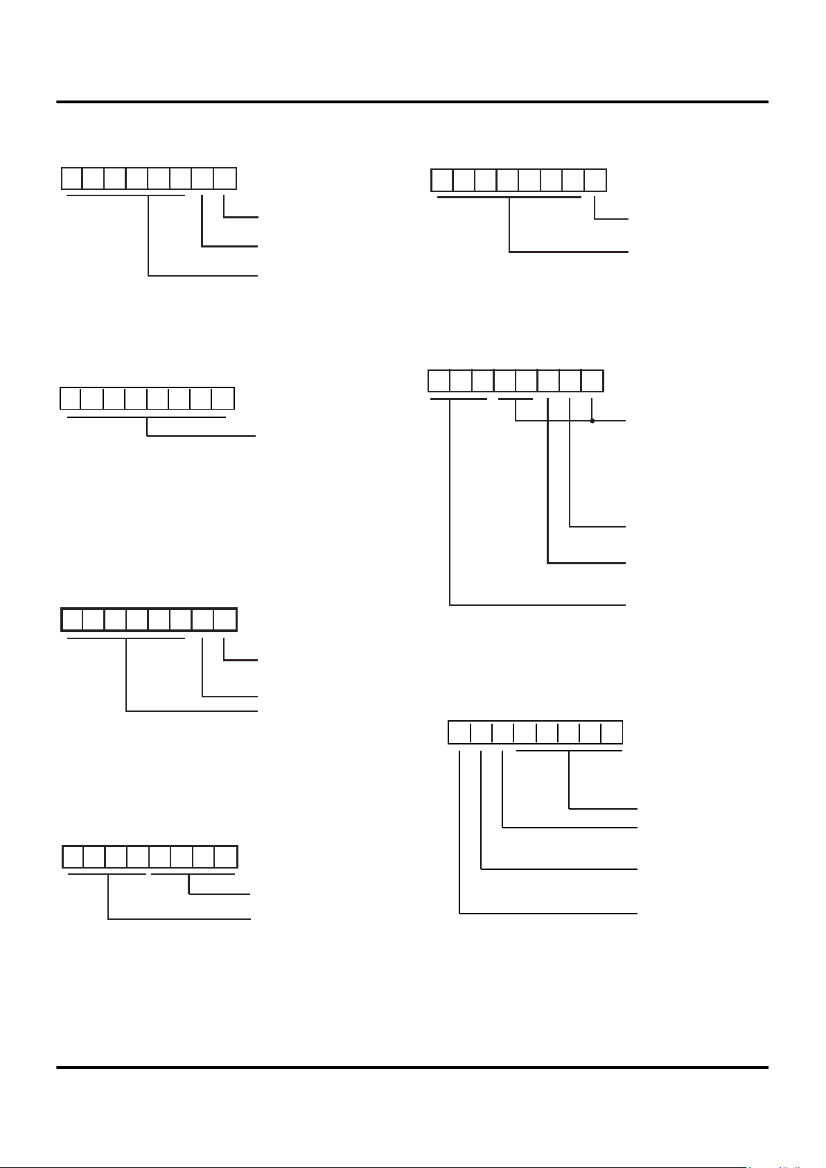
Z8 CONTROL REGISTER DIAGRAMS
Figure 19. Timer Mode Register
(F1H: Read/Write)
Figure 20. Counter/Timer 0 Register
(F4H: Read/Write)
Figure 21. Prescaler 0 Register
(F5H: Write Only)
Figure 22. Port 2 Mode Register
(F6
H
: Write Only)
D7 D6 D5 D4 D3 D2 D1 D0
0 = Disable T0 Count
1 = Enable T0 Count
0 = No Function
1 = Load T0
R241 TMR
Reserved (Must be 0)
D7 D6 D5 D4 D3 D2 D1 D0
T0 Initial Value
(When Written)
(Range 1-256 Decimal
01-00 HEX)
T0 Current Value
(When READ)
R244 T0
D7 D6 D5 D4 D3 D2 D1 D0
Count Mode
0
0 = T Single Pass
1 = T Modulo N
0
Reserved (Must be 0)
Prescaler Modulo
(Range: 1-64 Decimal
01-00 HEX)
R245 PRE0
D7 D6 D5 D4 D3 D2 D1 D0
P24-P27 I/O Definition
0 Defines Bit as OUTPUT
1 Defines Bit as INPUT
R246 P2M
Reserved
Figure 23. Port 2 Open Drain Register
(F7H: Write Only)
Figure 24. Interrupt Priority Register
(F9H: Write Only)
Figure 25. Interrupt Request Register
(FA
H
: Read/Write)
0 Port 2 Open-Drain
1 Port 2 Push-Pull
D7 D6 D5 D4 D3 D2 D1 D0
Reserved (Must be 0)
R247 P3M
D7 D6 D5 D4 D3 D2 D1 D0
Interrupt Group Priority
Reserved = 000
C > A > B = 001
A > B > C = 010
A > C > B = 011
B > C > A = 100
C > B > A = 101
B > A > C = 110
Reserved = 111
IRQ0, IRQ2 Priority (Group B)
0 = IRQ2 > IRQ0
1 = IRQ0 > IRQ2
IRQ1, IRQ4 Priority (Group C)
0 = IRQ1 > IRQ4
1 = IRQ4 > IRQ1
Reserved (Must be 0)
R249 IPR
D7 D6 D5 D4 D3 D2 D1 D0
R250 IRQ
IRQ0 = P32 Input
IRQ1 = P33 Input
IRQ2 = P31 Input
IRQ3 = USB
IRQ4 = T0
WDT During HALT
0 OFF *
1 ON
Stop Flag
0 POR/WDT*
1 Stop Recovery
* On RESET
WDT Hot Bit (Read Only)
0 POR*
1 WDT Timeout
Page 20

Z86U18
USB Device Controller with CMOS Z86K15 MCU Zilog
20 P R E L I M I N A R Y DS97KEY0102
Z8 CONTROL REGISTER DIAGRAMS (Continued)
Figure 26. Interrupt Mask Register
(FBH: Read/Write)
Figure 27. Flag Register
(FC
H
: Read/Write)
Figure 28. Register Pointer
(FD
H
: Read/Write)
D7 D6 D5 D4 D3 D2 D1 D0
1 Enables IRQ5-IRQ0
(D0 = IRQ0)
Reserved (Must be 0)
1=Global Interrupt Enable
0=Global Interrupt Disable
R251 IMR
D7 D6 D5 D4 D3 D2 D1 D0
User Flag F1
User Flag F2
Half Carry Flag
Decimal Adjust Flag
Overflow Flag
Sign Flag
Zero Flag
Carry Flag
R252 Flags
D7 D6 D5 D4 D3 D2 D1 D0
Bank Pointer
r4
R253 RP
r5
r6
r7
Register
Pointer
Figure 29. Stack Pointer
(FFH: Read/Write)
D7 D6 D5 D4 D3 D2 D1 D0
Stack Pointer Lower
Byte (SP0-SP7)
R255 SPL
Page 21

Z86U18
Zilog USB Device Controller with CMOS Z86K15 MCU
DS97KEY0102 P R E L I M I N A R Y 21
1
USB REGISTERS
REGISTER DESCRIPTIONS
Table 1. Address Offset
Located @ 01 in Expanded Register Space
Register Address Reset Value
Function Address 0 00
Endpoint 0 CSR 1 00
Endpoint 0 Write Count 2 00
Endpoint FIFO 3 00
IN CSR 4 40
IN FIFO 5 00
Interrupt Register 6 00
Miscellaneous Register 7 00
Figure 30. Function Address Register
D7 D6 D5 D4 D3 D2 D1 D0
Function Address
Not U sed
000h
Bit mC SIE Description
6:0 R/W R Upon receiving a SET_Address descriptor, the microcontroller writes this
register with the address received from the host.
Page 22

Z86U18
USB Device Controller with CMOS Z86K15 MCU Zilog
22 P R E L I M I N A R Y DS97KEY0102
REGISTER DESCRIPTIONS (Continued)
Figure 31. Endpoint 0 CS Register
D7 D6 D5 D4 D3 D2 D1 D0
Out _pkt _rdy
In _pkt _rdy
Force Stall
Data End
Setup End
Send Stall
Serviced Out Packet Ready
Serviced Setup End
001h
Bit No Bit Description mC SIE Description
7 Serviced Setup End W R The microcontroller writes a 1 to this register to clear setup end bit.
6 Serviced Outpacket
Ready
W R The microcontroller writes a 1 to this register to clear out packet ready
bit.
5 Send STALL W R If the microcontroller decodes an invalid descriptor, it writes a 1 to this
register before clearing out_pkt_rdy bit or when microcontroller decodes
a set feature or clear feature USB command from the host.
4 Setup End R W If the function receives a new setup transaction before the previous one
is complete (entire length of data is transferred), this bit is set. Upon
seeing this bit set, the microcontroller should abort the current set
operation.
3 Data End W R During the data phase of a control transfer after the microcontroller has
received/sent the last data as speciÞed in the setup phase, it sets this
bit.
2 Force STALL R W The SIE writes to this register, when it encounters a protocol violation,
and issues a STALL handshake to the current control transfer.
1 In Packet Ready W R During the data phase, after the microcontroller has Þlled the data, it sets
this bit. It is cleared by SIE upon successful transmittion of data.
0 Out Packet Ready R W The SIE sets this bit after writing data to the FIFO. The microcontroller
clears this bit by writing it to Serviced Out Packet Ready bit.
Figure 32. Endpoint 0 Write Count Register
D7 D6 D5 D4 D3 D2 D1 D0
Write Count
00000
002h
Bit mC SIE Description
2:0 R W The contents indicates the number of bytes in the FIFO.
Page 23

Z86U18
Zilog USB Device Controller with CMOS Z86K15 MCU
DS97KEY0102 P R E L I M I N A R Y 23
1
Figure 33. Endpoint 0 FIFO Register
D7 D6 D5 D4 D3 D2 D1 D0
FIFO Data
003 h
Bit mC SIE Description
7:0 R/W R/W This is the Endpoint 0 FIFO data register.
Figure 34. IN CS Register
000
D7 D6 D5 D4 D3 D2 D1 D0
In_pkt _rdy
Force Stall
IN MAXP
004 h
/Bit No Bit Description mC SIE Description
4:2 IN MAXP W R Before setting in_pkt_rdy, the microcontroller writes the maximum packet
size to these bits. The default value = 8 Bytes.
1 Force STALL R/W W The SIE writes this register, when it encounters a protocol violation, and
issues a STALL handshake to the current transfer. The microcontroller sets
this bit, when it receives a SET_FEATURE (ENDPOINT_STALL), and clears
it, when it receives a CLEAR_FEATURE (ENDPOINT_STALL).
0 In Packet Ready W R After the microcontroller has Þlled the data, it sets this bit. It is cleared by
SIE upon successful transmission of data.
Figure 35. IN FIFO Register
D7 D6 D5 D4 D3 D2 D1 D0
FIFO Data
005h
Bit mC SIE Description
7:0 W R The microcontroller writes IN data to this register.
Page 24

Z86U18
USB Device Controller with CMOS Z86K15 MCU Zilog
24 P R E L I M I N A R Y DS97KEY0102
REGISTER DESCRIPTIONS (Continued)
Figure 36. Interrupt Register
D7 D6 D5 D4 D3 D2 D1 D0
Endpoint 0 Interrupt
Suspend Interrupt
00000
IN Endpoint Interrupt
006h
Resume Interrupt
Bit No Bit Description mC SIE Description
3 Resume Interupt R W The ßag is sent on the Host signal to resume operations.
2 Suspend Interrupt R W The bit is set when theSuspend signaling is received from the host.
1 IN Endpoint Interrupt R W This bit is set upon:
1) clearing in_pkt_ rdy
2) setting Force STALL.
0 Endpoint 0 Interrupt R W This bit set by SIE upon:
1) setting out_pkt_rdy
2) clearing in_pkt_rdy
3) setting Force STALL
4) clearing data_end
5) setting data_end
Figure 37. Misc. Register
D7 D6 D5 D4 D3 D2 D1 D0
Suspend
Interrupt Mask Bits
000
Send Resume
007h
Bit No Bit Description mC SIE Description
4:2 Interrupt Mask Bits R/W R This has bit correspondence to the interrupt register. A value of 1, implies
that particular interrupt is disabled.
1 Send Resume W R The microcontroller writes a 1 to this bit, while in suspend mode, and
wants to start a resume sequence after the clocks are running. This bit is
set high for a duration of at least 10 ms by microcontroller.
0 Suspend R/W W This bit is set by the SIE when, the microcontroller is to enter suspend
mode. The microcontroller clears this bit after Þnishing resume signaling,
or after it receives a resume out interrupt, and the clocks have started.
Page 25

Z86U18
Zilog USB Device Controller with CMOS Z86K15 MCU
DS97KEY0102 P R E L I M I N A R Y 25
1
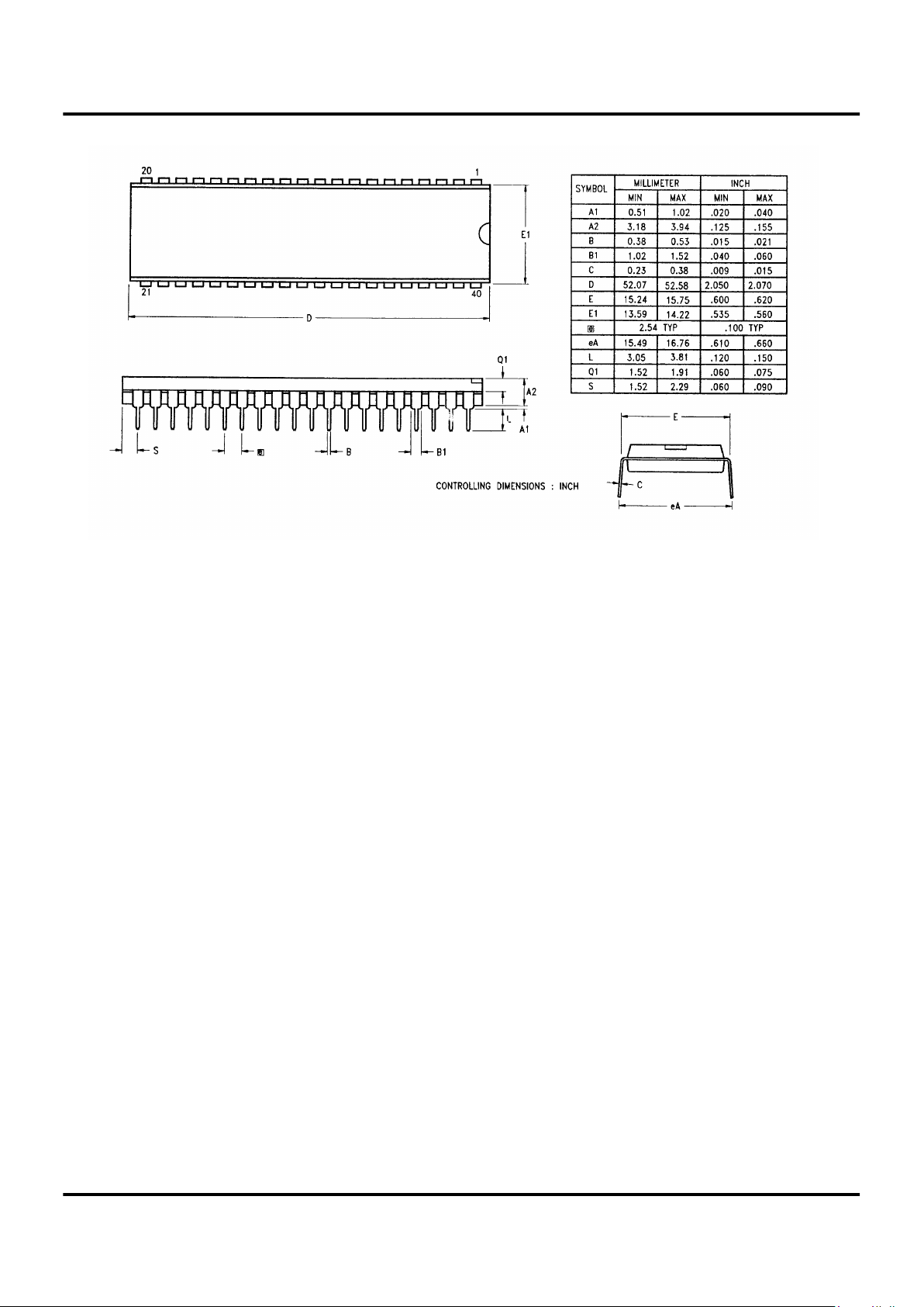
PACKAGE INFORMATION
Figure 38. 44-Pin QFP Package Diagram
Figure 39. 28-Pin SOIC
Page 26

Z86U18
USB Device Controller with CMOS Z86K15 MCU Zilog
26 P R E L I M I N A R Y DS97KEY0102
Figure 40. 28-Pin PDIP
Figure 41. 44-Pin PLCC
Page 27
Z86U18
Zilog USB Device Controller with CMOS Z86K15 MCU
DS97KEY0102 P R E L I M I N A R Y 27
1
Figure 42. 40-Pin DIP
Page 28

Z86U18
USB Device Controller with CMOS Z86K15 MCU Zilog
28 P R E L I M I N A R Y DS97KEY0102
ORDERING INFORMATION
For fast results, contact your Zilog sales office for assistance in ordering the part desired.
CODES
Package
P = Plastic DIP
V = Plastic Leaded Chip Carrier
F = Quad Flat Pack
Speed
06 = 6 MHz
Environment
C = Plastic Standard
Temperature
S = 0°C to +70°C
© 1997 by Zilog, Inc. All rights reserved. No part of this
document may be copied or reproduced in any form or by
any means without the prior written consent of Zilog, Inc.
The information in this document is subject to change
without notice. Devices sold by Zilog, Inc. are covered by
warranty and patent indemnification provisions appearing
in Zilog, Inc. Terms and Conditions of Sale only. Zilog, Inc.
makes no warranty, express, statutory, implied or by
description, regarding the information set forth herein or
regarding the freedom of the described devices from
intellectual property infringement. Zilog, Inc. makes no
warranty of merchantability or fitness for any purpose.
Zilog, Inc. shall not be responsible for any errors that may
appear in this document. Zilog, Inc. makes no commitment
to update or keep current the information contained in this
document.
ZilogÕs products are not authorized for use as critical
components in life support devices or systems unless a
specific written agreement pertaining to such intended use
is executed between the customer and Zilog prior to use.
Life support devices or systems are those which are
intended for surgical implantation into the body, or which
sustains life whose failure to perform, when properly used
in accordance with instructions for use provided in the
labeling, can be reasonably expected to result in
significant injury to the user.
Zilog, Inc. 210 East Hacienda Ave.
Campbell, CA 95008-6600
Telephone (408) 370-8000
FAX 408 370-8056
Internet: http://www.zilog.com
6 MHz 6 MHz 6 MHz 6 MHz 6 MHz
40-Pin DIP 44-Pin PLCC 44-PIN QFP 28-Pin DIP 28-Pin SOIC
Z86U18PSC Z86U18VSC Z86U18FSC Z86U18PSC Z86U18SSC
Example:
Z 86U18 05 P S C
Environmental Flow
Temperature
Package
Speed
Product Number
Zilog Prefix
is a Z86U18, 6 MHz, DIP, 0°C to +70°C, Plastic Standard Flow
Page 29

Z86U18
Zilog USB Device Controller with CMOS Z86K15 MCU
DS97KEY0102 P R E L I M I N A R Y 29
1
Page 30

Z86U18
USB Device Controller with CMOS Z86K15 MCU Zilog
30 P R E L I M I N A R Y DS97KEY0102
 Loading...