

Page 1
FEATURES
PRELIMINARY
PRELIMINARY
CUSTOMER PROCUREMENT SPECIFICATION
Z86L88/L81/L86
INFRARED REMOTE CONTROLLERS
Z86L88/L81/L86
CP96LVO1201
ROM RAM* 28-pin
Part (KB) (Bytes) I/O DIP, SOIC
Z86L88 1 6 237 2 4 X
Z86L81 2 4 237 2 4 X
Z86L86 3 2 237 2 4 X
*General-Purpose
■ 2.0V to 3.9V Operating Range (8.0 MHz)
■ Three Standby Modes (Typical)
– STOP - 2 µA
– HALT - 0.8 mA
– Low-Voltage Standby (< VLV)
■ Expanded Register File Control Registers
■ Special Architecture to Automate Both Generation
and Reception of Complex Pulses or Signals:
– One Programmable 8-Bit Counter/Timer
with Two Capture Registers
– One Programmable 16-Bit Counter/Timer
with One Capture Register
– Programmable Input Glitch Filter
for Pulse Reception
■ Five Priority Interrupts
■ Low-Voltage Detection and Protection
■ Watch-Dog Timer (WDT)/Power-On Reset (POR)
■ Two Independent Comparators with Programmable
Interrupt Polarity
■ On-Chip Oscillator that Accepts a Crystal, Ceramic
Resonator, LC, or External Clock Drive
■ Mask Selectable 200 kOhms Pull-Ups on Ports 0, 2, 3
– All Eight Port 2 Bits at One Time or Not
– Pull-Ups Automatically Disabled Upon
Selecting Individual Pins as Outputs
■ Maskable 0.4 V
Through P03 for Direct Mouse/Trackball IR Sensor
Interface
■ Low-Voltage Standby Mode
Single Trip Point Inputs on P00
DD
GENERAL DESCRIPTION
The Z86L8X family of infrared (IR) consumer controller
processors are ROM-based members of the Z8® singlechip microcontroller family offering a unique register-toregister architecture that avoids accumulator bottlenecks
and offers fast execution of code.
Zilog's CMOS microcontrollers feature fast execution,
efficient use of memory, sophisticated interrupts, input/
output bit manipulation capabilities, automated pulse
generation/reception, and easy hardware/software system
expansion along with low-cost and low-power consumption.
CP96LVO1201 (6/96)
The Z86L8X family architecture is based on Zilog's 8-bit
microcontroller core with an Expanded Register File (ERF)
to allow access to register mapped peripherals, I/O circuits,
and powerful counter/timer circuitry. The Z86L8X offers a
flexible I/O scheme, an efficient register and address
space structure, and a number of ancillary features that
are useful in many consumer, automotive, computer
peripheral, and battery operated hand-held applications.
1
Page 2
PRELIMINARY
GENERAL DESCRIPTION (Continued)
Z86L88/L81/L86
CP96LVO1201
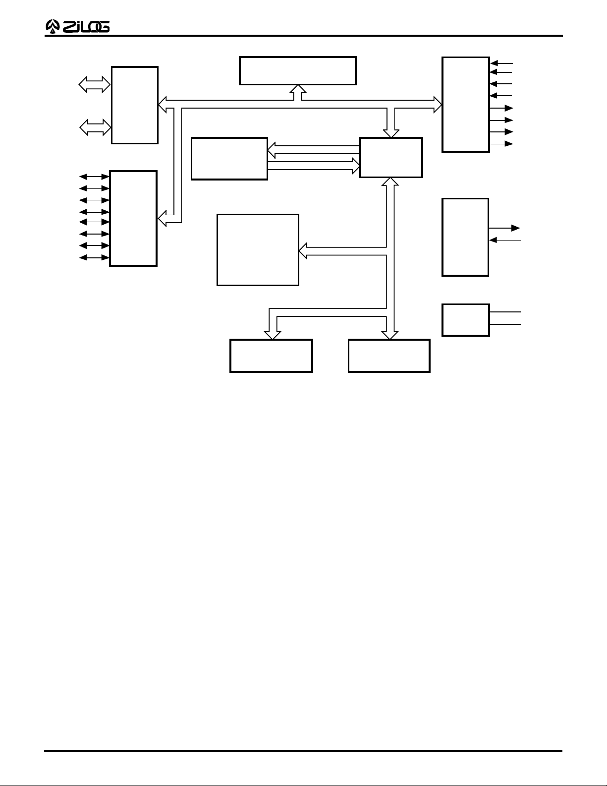
For applications demanding powerful I/O capabilities, the
Z86L8X fulfills this with two package options in which 24
pins of dedicated input and output are grouped into three
ports. Each port consists of eight lines and is configurable
under software control to provide timing, status signals,
and parallel I/O.
There are three basic address spaces available to support
a wide range of configurations: Program Memory, Register
File, and Expanded Register File. (ERF). The Register File
is composed of 256 bytes of RAM. It includes four I/O port
registers, 15 control and status registers, and the rest are
general purpose registers. The ERF consists of two register groups (Banks D and F).
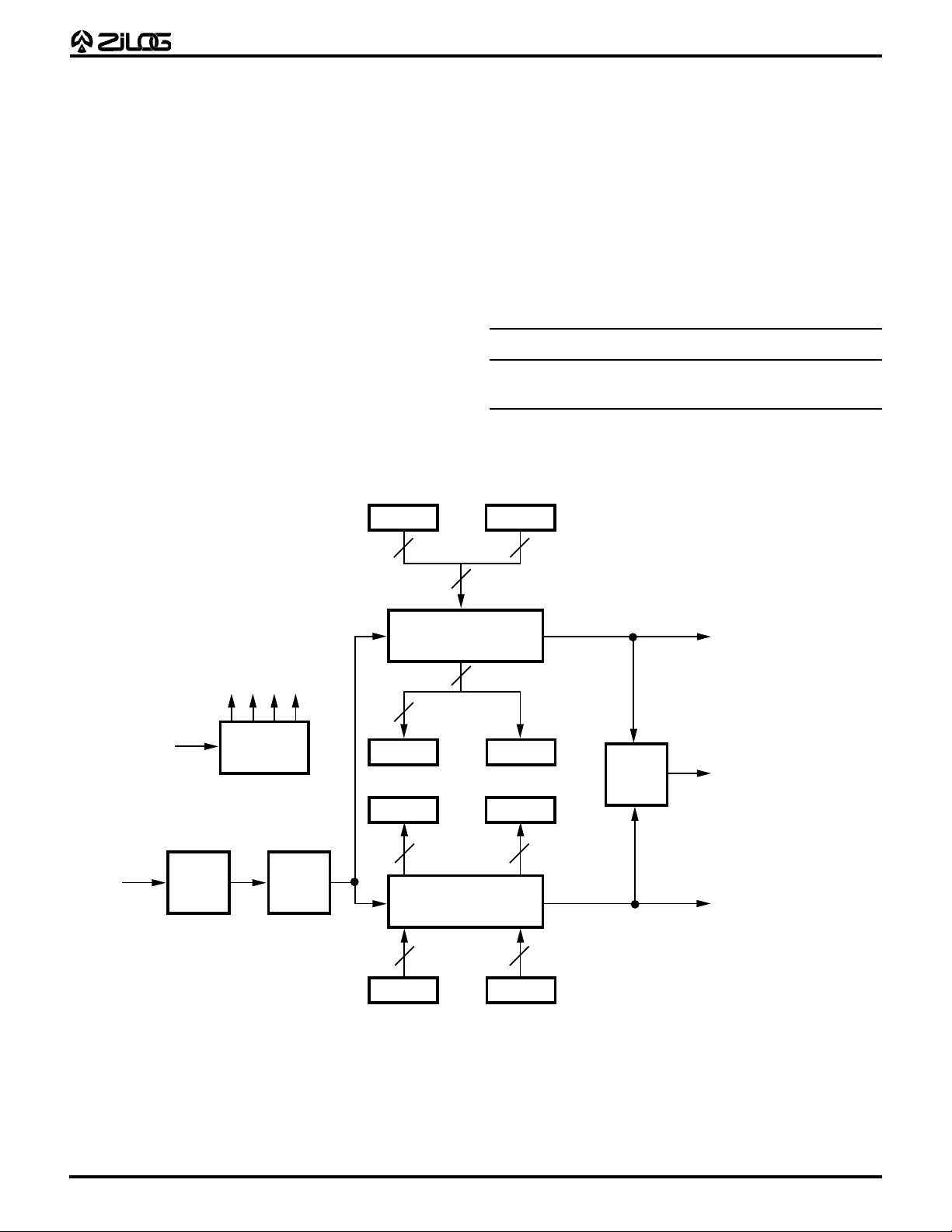
To unburden the program from coping with such real-time
problems as generating complex waveforms or receiving
HI16 LO16
8
and demodulating complex waveform/pulses, the Z86L8X
offers a new intelligent counter/timer architecture with 8-bit
and 16-bit counter/timers (Figure 1). Also included are a
large number of user-selectable modes, and two on-board
comparators to process analog signals with separate
reference voltages (Figure 2).
Notes:
All Signals with a preceding front slash, "/", are active Low, e.g.,
B//W (WORD is active Low); /B/W (BYTE is active Low, only).
Power connections follow conventional descriptions below:
Connection Circuit Device
Power V
Ground GND V
8
CC
V
DD
SS
Input
SCLK
Glitch
Filter
1248
Clock
Divider
Edge
Detect
Circuit
16
16-Bit
T16
16
8
TC16H TC16L
HI8 LO8
8
8-Bit
T8
8
TC8H TC8L
Timer 16
And/Or
Logic
8
8
Timer 8/16
Timer 8
Figure 1. Counter/Timer Block Diagram
2
Page 3
PRELIMINARY
Z86L88/L81/L86
CP96LVO1201
P00
P01
P02
P03
P04
P05
P06
P07
P20
P21
P22
P23
P24
P25
P26
P27
Port 0
Port 2
Register Bus
ROM
8K/4K x 8
Extended
Register
Counter/Timer 8
Register File
256 x 8-Bit
Internal Data Bus
File
8-Bit
Internal
Address Bus
Extended
Register Bus
Z8 Core
Counter/Timer 16
16-Bit
Port 3
Machine
Timing
&
Instruction
Control
Power
Pref1
P31
P32
P33
P34
P35
P36
P37
XTAL
VDD
VSS
Figure 2. Functional Block Diagram
3
Page 4
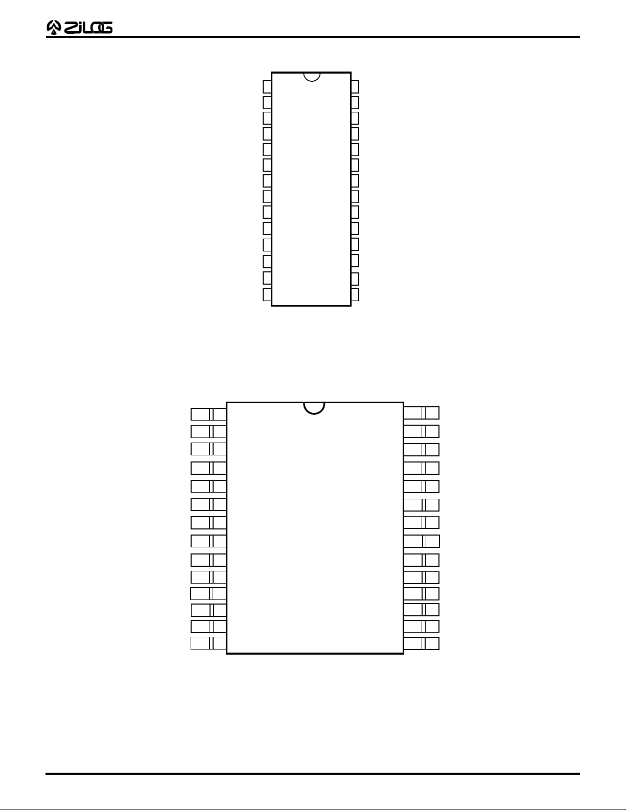
PIN DESCRIPTION
PRELIMINARY
Z86L88/L81/L86
CP96LVO1201
P25
P26
P27
P04
P05
P06
P07
VDD
XTAL2
XTAL1
P31
P32
P33
P34
1
2
3
4
5
6
7
8
9
10
11
12
13
Z86L88/
L81/L86
DIP
28
27
26
25
24
23
22
21
20
19
18
17
16
1514
Figure 3. 28-Pin DIP
Pin Assignments
P24
P23
P22
P21
P20
P03
VSS
P02
P01
P00
PREF1
P36
P37
P35
P25
P26
P27
P04
P05
P06
P07
VDD
XTAL2
XTAL1
P31
P32
P33
P34
1
2
3
4
5
6
7
8
9
10
11
12
13
14
Z86L88/L81/L86
SOIC
Figure 4. 28-Pin SOIC
Pin Assignments
28
27
26
25
24
23
22
21
20
19
18
17
16
15
P24
P23
P22
P21
P20
P03
VSS
P02
P01
P00
PREF1
P36
P37
P35
4
Page 5

PRELIMINARY
PIN DESCRIPTION (Continued)
Table 1. Pin Identification
28-Pin
DIP & SOIC # Symbol Direction Description
1 P2 5 Input/Output
2 P2 6 Input/Output
3 P2 7 Input/Output
4 P0 4 Input/Output Port 0 can be configured as a mouse/trackball input.
5 P05 Input/Output
6 P06 Input/Output
7 P07 Input/Output
8V
DD
9 XTAL2 Output Crystal, Oscillator Clock
1 0 XTAL1 Input Crystal, Oscillator Clock
11 P31 Input IRQ2/Modulator Input/Comparator 1 Input
12 P32 Input IRQ0/Comparator 2 Input
13 P33 Input IRQ1/Comparator 2 Ref
14 P34 Output T8 Output
15 P35 Output T16 Output
16 P37 Output
Power Supply
Z86L88/L81/L86
CP96LVO1201
17 P36 Output T8/T16 Output
18 Pref1 Input Analog Ref Input (Comparator 1)
19 P00 Input/Output Port 0 is Nibble Programmable.
20 P01 Input/Output Port 0 can be configured as A15-A8 external program.
21 P02 Input/Output
22 V
SS
Ground
23 P03 Output ROM Address Bus
24 P20 Input/Output Port 2 pins are individually configurable as input or output.
25 P21 Input/Output
26 P22 Input/Output
27 P23 Input/Output
28 P24 Input/Output
5
Page 6

ABSOLUTE MAXIMUM RATINGS
PRELIMINARY
Z86L88/L81/L86
CP96LVO1201
Symbol Description Min Max Units
V
CC
T
STG
T
A
Notes:
* Voltage on all pins with respect to GND.
† See Ordering Information.
Supply Voltage (*) –0.3 +7.0 V
Storage Temp. –65° +150° C
Oper. Ambient Temp. † C
STANDARD TEST CONDITIONS
The characteristics listed below apply for standard test
conditions as noted. All voltages are referenced to GND.
Positive current flows into the referenced pin (Figure 5).
Stresses greater than those listed under Absolute Maxi-
mum Ratings may cause permanent damage to the de-
vice. This is a stress rating only; operation of the device at
any condition above those indicated in the operational
sections of these specifications is not implied. Exposure to
absolute maximum rating conditions for an extended pe-
riod may affect device reliability.
From Output
Under Test
I
150 pF
Figure 5. Test Load Diagram
CAPACITANCE
TA = 25°C, VCC = GND = 0V, f = 1.0 MHz, unmeasured pins returned to GND.
Parameter Max
Input capacitance 12 pF
Output capacitance 12 pF
I/O capacitance 12 pF
6
Page 7

DC CHARACTERISTICS
Sym Parameter V
Max Input Voltage 2.0V 7 V IIN <250 µA
V
Clock Input 2.0V 0.9 V
CH
High Voltage Clock Generator
PRELIMINARY
TA = 0°C to +70°C Typ @
CC
Min Max 25°C Units Conditions Notes [3]
3.9V 7 V IIN <250 µA
VCC + 0.3 V Driven by External
CC
3.9V 0.9 V
VCC + 0.3 V Driven by External
CC
Clock Generator
Z86L88/L81/L86
CP96LVO1201
V
V
V
V
V
V
V
V
V
I
I
I
I
IL
OL
IR
CC
Clock Input 2.0V VSS – 0.3 0.2 V
CL
CC
V Driven by External
Low Voltage Clock Generator
3.9V VSS– 0.3 0.2 V
CC
V Driven by External
Clock Generator
Input High Voltage 2.0V 0.7 V
IH
3.9V 0.7 V
Input Low Voltage 2.0V VSS – 0.3 0.2 V
IL
3.9V VSS – 0.3 0.2 V
Output High Voltage 2.0V VCC – 0.4 1.7 V IOH = –0.5 mA †
OH1
VCC + 0.3 1.3 V
CC
VCC + 0.3 2.5 V
CC
CC
CC
0.5 V
0.9 V
3.9V VCC – 0.4 3.7 V IOH = –0.5 mA
Output High Voltage 2.0V VCC – 0.7 1.5 V IOH = –7 mA [10]
OH2
(P36, P37) 3.9V VCC – 0.7 3.5 V I
Output Low Voltage 2.0V 0.4 0.1 V IOL = 1.0 mA *
OL1
,= –7 mA [10]
OH
3.9V 0.4 0.2 V IOL = 4.0 mA
Output Low Voltage 2.0V 0.8 0.6 V I
OL2
= 5.0 mA *
OL
3.9V 0.8 0.3 V IOL = 7.0 mA
Output Low Voltage 2.0V 0.8 0.3 V I
OL2
(P00, P01, P36, P37) 3.9V 0.8 0.2 V I
Comparator Input 2.0V 25 10 m V
OFFSET
= 10 mA [9]
OL
= 10 mA [9]
OL
Offset Voltage 3.9V 25 10 mV
Input Leakage 2.0V –1 1 < 1 µ AV
3.9V –1 1 < 1 µ AV
Output Leakage 2.0V –1 1 < 1 µ AV
3.9V –1 1 < 1 µ AV
= OV, V
IN
= OV, V
IN
= OV, V
IN
= OV, V
IN
CC
CC
CC
CC
Reset Input Current 2.0V –45 –20 µ A
3.9V –55 –30 µ A
Supply Current 2.0V 10 4 mA @ 8.0 MHz [4, 5]
3.9V 15 10 mA @ 8.0 MHz [4, 5]
2.0V 100 10 µ A @ 32 kHz [4, 5,11]
3.9V 300 10 µ A @ 32 kHz [4, 5,11]
7
Page 8

DC CHARACTERISTICS (Continued)
Sym Parameter V
CC
PRELIMINARY
Z86L88/L81/L86
CP96LVO1201
TA = 0°C to +70°C Typ @
Min Max 25°C Units Conditions Notes [3]
I
CC1
Standby Current 2.0V 3 1 m A HALT Mode [4,5]
(WDT Off) VIN = OV, V
CC
@ 8.0 MHz
3.9V 5 4 mA HALT Mode [4,5]
VIN = OV, V
CC
@ 8.0 MHz
2.0V 2 0.8 m A Clock Divide-by-16 [4,5]
@ 8.0 MHz
3.9V 4 2.5 m A Clock Divide-by-16 [4,5]
@ 8.0 MHz
I
CC2
Standby Current 2.0V 8 2 µ A STOP Mode [6,8]
VIN = OV, V
CC
WDT is not Running
3.9V 10 3 µ A STOP Mode [6,8]
VIN = OV, V
CC
WDT is not Running
2.0V 500 310 µ A STOP Mode [6,8]
VIN = OV, V
CC
WDT is Running
3.9V 800 600 µ A STOP Mode [6,8]
VIN = OV, V
CC
WDT is Running
T
Power-On Reset 2.0V 7.5 75 13 ms
POR
3.9V 2.5 20 7 ms
V
VCC Low Voltage Protection 2.15 1.7 V 8 MHz max [7]
L V
Ext. CLK Freq.
Notes:
[1] I
CC1
Crystal/Resonator 4.0 mA 5 mA 8.0 MHz
External Clock Drive 0.3 mA 5 mA 8.0 MHz
[2] GND = 0V
[3] 2.0V to 3.9V
[4] All outputs unloaded, I/O pins floating, inputs at rail.
[5] CL1 = CL2 = 100 pF
[6] Same as note [4] except inputs at VCC.
[7] The V
[8] Oscillator stopped.
[9] Two outputs at a time, independent to other outputs.
[10] One at a time.
[11] 32 kHz clock driver input.
† All outputs excluding P36, P37.
* All outputs excluding P36, P37, P00, and P01.
increases as the temperature decreases.
LV
Typ Max Unit Frequency
8
Page 9

AC CHARACTERISTICS
Additional Timing Diagram
PRELIMINARY
Z86L88/L81/L86
CP96LVO1201
Clock
T
IN
IRQ
N
Clock
Setup
Stop
Mode
Recovery
Source
7 7
8
1
2 2 3
4
5
6
9
10
3
11
Figure 6. Additional Timing
9
Page 10

PRELIMINARY
Z86L88/L81/L86
CP96LVO1201
AC CHARACTERISTICS
Additional Timing Table
TA = 0°C to +70°C
V
CC
No Symbol Parameter Note [3] M i n M a x Units Notes
1 T pC Input Clock Period 2.0V 121 DC ns [1]
3.9V 121 DC ns [1]
2 TrC,TfC Clock Input Rise 2.0V 25 ns [1]
and Fall Times 3.9V 25 ns [1]
3 T w C Input Clock Width 2.0V 37 ns [1]
3.9V 37 ns [1]
4 TwTinL Timer Input 2.0V 100 ns [1]
Low Width 3.9V 70 ns [1]
5 TwTinH Timer Input 2.0V 3TpC [1]
High Width 3.9V 3TpC [1]
6 TpTin Timer Input Period 2.0V 8TpC [1]
3.9V 8TpC [1]
7 TrTin,TfTin Timer Input Rise 2.0V 100 ns [1]
and Fall Timers 3.9V 100 ns [1]
8A TwIL Interrupt Request 2.0V 100 ns [1, 2]
Low Time 3.9V 70 ns [1, 2]
8.0 MHz
8B TwIL Int. Request 2.0V 3TpC [1, 3]
Low Time 3.9V 3TpC [1, 3]
9 TwIH Interrupt Request 2.0V 3TpC [1, 2]
Input High Time 3.9V 3TpC [1, 2]
10 Twsm Stop-Mode Recovery 2.0V 12 ns [8]
Width Spec 3.9V 12 ns [8]
2.0V 5TpC [7]
3.9V 5TpC [7]
11 Tost Oscillator 2.0V 5TpC [4]
Start-up Time 3.9V 5TpC [4]
12 Twdt Watch-Dog Timer (5 ms) 2.0V 12 75 ms D0 = 0 [5]
Delay Time 3.9V 5 20 ms D1 = 0 [5]
(15 ms) 2.0V 25 150 ms D0 = 1 [5]
3.9V 10 40 ms D1 = 0 [5]
(25 ms) 2.0V 50 300 ms D0 = 0 [5]
3.9V 25 80 ms D1 = 1 [5]
(100 ms) 2.0V 225 1200 ms D0 = 1 [5]
3.9V 100 320 ms D1 = 1 [5]
Notes:
[1] Timing Reference uses 0.9 VCC for a logic 1 and 0.1 VCC for a logic 0.
[2] Interrupt request through Port 3 (P33-P31).
[3] Interrupt request through Port 3 (P30).
[4] SMR – D5 = 0
[5] Reg. WDTMR
[6] 2.0V to 3.9V
[7] Reg. SMR – D5 = 0
[8] Reg. SMR – D5 = 1
10
Page 11

PRELIMINARY
Z86L88/L81/L86
CP96LVO1201
© 1996 by Zilog, Inc. All rights reserved. No part of this document
may be copied or reproduced in any form or by any means
without the prior written consent of Zilog, Inc. The information in
this document is subject to change without notice. Devices sold
by Zilog, Inc. are covered by warranty and patent indemnification
provisions appearing in Zilog, Inc. Terms and Conditions of Sale
only. Zilog, Inc. makes no warranty, express, statutory, implied or
by description, regarding the information set forth herein or
regarding the freedom of the described devices from intellectual
property infringement. Zilog, Inc. makes no warranty of merchantability or fitness for any purpose. Zilog, Inc. shall not be
responsible for any errors that may appear in this document.
Zilog, Inc. makes no commitment to update or keep current the
information contained in this document.
Zilog’s products are not authorized for use as critical components in life support devices or systems unless a specific written
agreement pertaining to such intended use is executed between
the customer and Zilog prior to use. Life support devices or
systems are those which are intended for surgical implantation
into the body, or which sustains life whose failure to perform,
when properly used in accordance with instructions for use
provided in the labeling, can be reasonably expected to result in
significant injury to the user.
Zilog, Inc. 210 East Hacienda Ave.
Campbell, CA 95008-6600
Telephone (408) 370-8000
FAX 408 370-8056
Internet: http://www.zilog.com
11
 Loading...