

Page 1
CP96DZ83200 (10/96)
P R E L I M I N A R Y
1
1
P
RELIMINARY
C
USTOMER
P
ROCUREMENT
S
PECIFICATION
Z86E64
1
CMOS Z8 OTP M
ICROCONTROLLER
FEATURES
■
Low-Power Consumption: 200 mW (max)
■
Fast Instruction Pointer: 0.75 µ s @ 16 MHz
■
Two Standby Modes: STOP and HALT
■
Full-Duplex UART
■
All Digital Inputs are TTL Levels
■
Auto Latches
■
RAM and ROM Protect
■
Two Programmable 8-Bit Counter/Timers,
Each with 6-Bit Programmable Prescaler
■
Six Vectored, Priority Interrupts from Eight Different
Sources
■
Low EMI Mode Option
■
68-Pin Leaded Chip-Carrier
GENERAL DESCRIPTION
The Z86E64 is a member of the Z8 single-chip microcontroller family. The Z86E64 can address both external memory and pre-programmed ROM, which enables this Z8
MCU
TM
to be used in high-volume applications where
code flexibility is required.
The Z86E64 is a pin compatible, One-Time-Programmable
(OTP) version of the Z86C64. The Z86E64 contains 32 KB
of EPROM memory in place of the 32 KB of ROM on the
Z86C64.
There are three basic address spaces available to support
this wide range of configuration: Program Memory, Data
Memory, and 236 general-purpose registers.
The Z86E64 offers a flexible I/O scheme, an efficient register and address space structure, multiplexed capabilities
between address/data, I/O, and a number of ancillary features that are useful in many industrial and advanced scientific applications.
For applications demanding powerful I/O capabilities, the
Z86E64’s dedicated input and output lines are grouped
into six ports. Each port consists of eight lines, except port
6, which has four lines. Each port is configurable under
software control to provide timing, status signals, serial or
parallel I/O with or without handshake, and an address/data bus for interfacing external memory.
The Z86E64 offers two on-chip counter/timers with a large
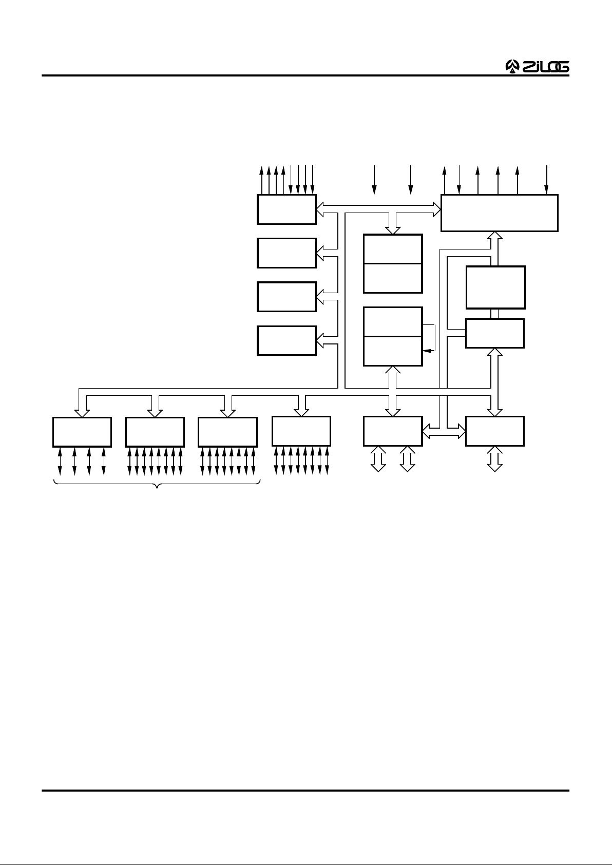
number of user-selectable modes, and an Universal Asynchronous Receiver/Transmitter (UART). See figure 1 forFunctional Block description.
Note: All Signals with a preceding front slash, "/", are ac-
tive Low, for example: B//W (WORD is active Low); /B/W
(BYTE is active Low, only). Power connections follow conventional descriptions below:
Device
ROM
(KB)
RAM*
(Bytes)
I/O
Lines
Voltage
Range
Z86E64 32 236 52 4.5-5V
Note: *General-Purpose
Connection Circuit Device
Power V
CC
V
DD
Ground GND V
SS
Page 2
Z86E64
CMOS Z8 OTP Microcontroller
2
P R E L I M I N A R Y
CP96DZ83200
GENERAL DESCRIPTION (Continued)
Figure 1. Z86E64 Functional Block Diagram
Port 3
Counter/
Timers (2)
Interrupt
Control
Port 2
ALU
Flags
Register
Pointer
Register File
256 x 8-Bit
Machine Timing and
Instruction Control
Program
Counter
Vcc GND XTAL
R//W /RESETOutput Input
UART
Port 0 Port 1
Address or I/O
(Nibble Programmable)
Address/Data or I/O
(Byte Programmable)
44 8
/AS /DS
Port 4Port 5Port 6
I/O
(Bit Programmable)
I/O
(Bit Programmable)
Program
Memory
32,768 x 8-Bit
Page 3
Z86E64
CMOS Z8 OTP Microcontroller
CP96DZ83200
P R E L I M I N A R Y
3
1
PIN DESCRIPTION
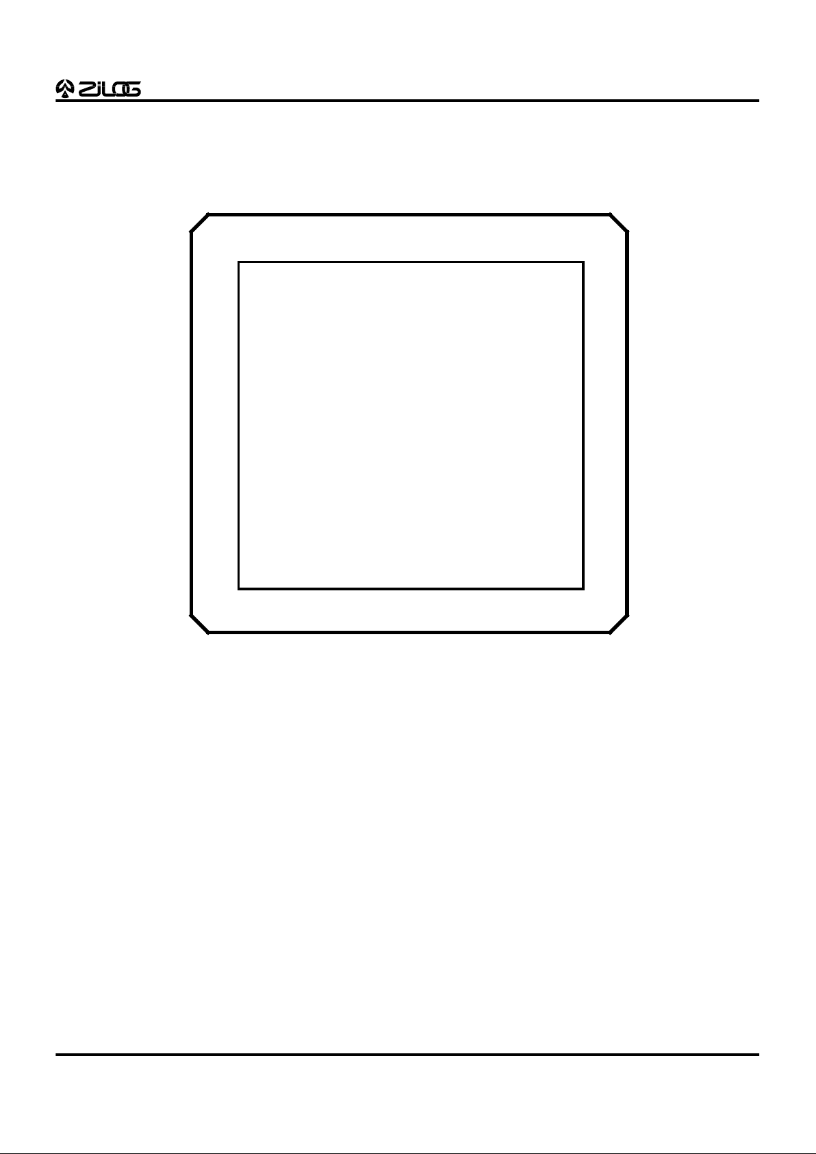
Figure 2. Z86E64 68-Pin PLCC Pin Assignments
Z86E64
PLCC
10
11
12
13
14
15
16
17
18
19
20
21
22
23
24
25
26
27 28 29 30 31 32 33 34 35 36 37 38 39 40 41 42 43
/Reset
P30
P37
XTAL1
XTAL2
P45
VCC
P44
P43
P42
P36
P31
P41
P40
P26
P25
P27
P54
VCC
P07
P14
P13
P12
P57
P56
P11
P10
P55
P53
P52
P06
P04
P03
P05
789 6543216867666564636261
60
59
58
57
56
55
54
53
52
51
50
49
48
47
46
45
44
P24
P23
P22
P60
P61
P21
P20
SCLK
/SYNC
GND
P33
P34
P62
P63
P17
P16
P15
R//W
/P0DS
/DS
P46
P47
/P1DS
/AS
/DTimers
P35
/ROMless
GND
P32
P50
P51
P00
P01
P02
Page 4
Z86E64
CMOS Z8 OTP Microcontroller
4
P R E L I M I N A R Y
CP96DZ83200
PIN DESCRIPTION (Continued)
Table 1. Z86E64 68-Pin PLCC Pin Identification
Pin # Symbol Function Direction
1-2 P44-P43 Port 4, Pins 3,4 In/Output
3 VCC Power Supply Input
4 P45 Port 4, Pin 5 In/Output
5 XTAL2 Crystal, Oscillator Clock Output
6 XTAL1 Crystal, Oscillator Clock Input
7 P37 Port 3, Pin 7 Output
8 P30 Port 3, Pin 0 Input
9 /RESET Reset Input
10 R//W Read/Write Output
11 /P0DS Port 0 Data Strobe Output
12 /DS Data Strobe Output
13-14 P47-P46 Port 4, Pins 6,7 In/Output
15 /P1DS Port 1, Data Strobe Output
16 /AS Address Strobe Output
17 /DTIMER DTIMER Input
18 P35 Port 3, Pin 5 Output
19 /ROMless ROM/ROMless control Input
20 GND Ground Input
21 P32 Port 3, Pin 2 Input
22-23 P51-P50 Port 5, Pins 0,1 In/Output
24-31 P07-P00 Port 0, Pins 0,1,2,3,4,5,6,7 In/Output
32 VCC Power Supply Input
33-36 P55-P52 Port 5, Pins 2,3,4,5 In/Output
37-38 P11-P10 Port 1, Pins 0,1 In/Output
39-40 P56-P57 Port 5, Pins 6,7 In/Output
41-46 P17-P12 Port 1, Pins 2,3,4,5,6,7 In/Output
47-48 P63-P62 Port 6, Pins 3,2 In/Output
49 P34 Port 3, Pin 4 Output
50 P33 Port 3, Pin 3 Input
51 GND Ground Input
52 /SYNC Synchronization Output
53 SCLK System Clock Output
54-55 P21-P20 Port 2, Pins 0,1 In/Output
56-57 P60-P61 Port 6, Pins 1,0 In/Output
58-63 P27-P22 Port 2, Pins 2,3,4,5,6,7 In/Output
64-65 P41-P40 Port 4, Pins 0,1 In/Output
66 P31 Port 3, Pin 1 Input
67 P36 Port 3, Pin 6 Output
68 P42 Port 4, Pin 2 In/Output
Page 5

Z86E64
CMOS Z8 OTP Microcontroller
CP96DZ83200
P R E L I M I N A R Y
5
1
DC CHARACTERISTICS
V
CC
= 4.5V to 5.5V
TA = 0 ° C to +70 ° C Typical at
Sym Parameter Min Max 25 ° C Units Conditions
Max Input Voltage 7 V I
IN
<250 µ A
Max Input Voltage 12.5V V P30-P33 Only in OTP mode
V
CH
Clock Input High Voltage 3.8 VCC V Driven by External Clock Generator
V
CL
Clock Input Low Voltage –0.3 0.8 V Driven by External Clock Generator
V
IH
Input High Voltage 2.0 VCC V
V
IL
Input Low Voltage –0.3 0.8 V
V
OH
Output High Voltage 2.4 V I
OH
= –2.0 mA
V
OL
Output Low Voltage 0.4 V I
OL
= +2.0 mA
V
RH
Reset Input High Voltage 3.8 VCC V
V
Rl
Reset Input Low Voltage –0.3 0.8 V
I
IL
Input Leakage –10 10
µ
A 0V < V
IN
< +5.25V
I
OL
Output Leakage –10 10
µ
A 0V < V
IN
< +5.25V
I
IR
Reset Input Current –50
µ
AV
CC
= +5.25V, VRL = 0V
I
CC
Supply Current 50 25 mA @ 12 MHz
60 35 mA @ 16 MHz
I
CC1
Standby Current 15 5 mA
20 10 mA HALT Mode V
IN
= 0V, V
CC
@ 16 MHz
I
CC2
Standby Current 20 5
µ
A STOP Mode V
IN
= 0V, V
CC
@ 12 MHz
20 5
µ
A STOP Mode V
IN
= 0V, V
CC
@ 16MHz
Page 6

Z86E64
CMOS Z8 OTP Microcontroller
6
P R E L I M I N A R Y
CP96DZ83200
AC CHARACTERISTICS
External I/O or Memory Read or Write Timing Diagram
Figure 3. External I/O or Memory Read/Write Timing
R//W
9
12
19
3
16
13
4
5
8
18
11
6
17
10
15
7
14
21
Port 0, /DM
Port 1
/AS
/DS
(Read)
Port 1
/DS
(Write)
A - A
07
D - D IN
07
D - D OUT
07
A - A
07
Page 7

Z86E64
CMOS Z8 OTP Microcontroller
CP96DZ83200
P R E L I M I N A R Y
7
1
External I/O or Memory Read and Write Timing Table
V
CC
= 4.5V to 5.5V
TA = 0 ° C to 70 ° C
12 MHz 16 MHz
No Symbol Parameter Min Max Min Max Units Notes
1 TdA(AS) Address Valid to /AS Rise Delay 35 20 ns [2,3]
2 TdAS(A) /AS Rise to Address Float Delay 45 30 ns [2,3]
3 TdAS(DR) /AS Rise to Read Data Req’d Valid 220 180 ns [1,2,3]
4 TwAS /AS Low Width 55 35 ns [2,3]
5 TdAZ(DS) Address Float to /DS Fall 0 0 ns
6 TwDSR /DS (Read) Low Width 185 135 ns [1,2,3]
7 TwDSW /DS (Write) Low Width 110 80 ns [1,2,3]
8 TdDSR(DR) /DS Fall to Read Data Req’d Valid 130 75 ns [1,2,3]
9 ThDR(DS) Read Data to /DS Rise Hold Time 0 0 ns [2,3]
10 TdDS(A) /DS Rise to Address Active Delay 45 35 ns [2,3]
11 TdDS(AS) /DS Rise to /AS Fall Delay 55 30 ns [2,3]
12 TdR/W(AS) R//W Valid to /AS Rise Delay 30 20 ns [2,3]
13 TdDS(R/W) /DS Rise to R//W Not Valid 35 30 ns [2,3]
14 TdDW(DSW) Write Data Valid to /DS Fall (Write) Delay 35 25 ns [2,3]
15 TdDS(DW) /DS Rise to Write Data Not Valid Delay 35 30 ns [2,3]
16 TdA(DR) Address Valid to Read Data Req’d Valid 255 200 ns [1,2,3]
17 TdAS(DS) /AS Rise to /DS Fall Delay 55 40 ns [2,3]
18 TdDI(DS) Data Input Setup to /DS Rise 75 60 ns [1,2,3]
19 TdDM(AS) /DM Valid to /AS Fall Delay 50 30 ns [2,3]
Notes:
[1] When using extended memory timing add 2 TpC.
[2] Timing numbers given are for minimum TpC.
[3] See clock cycle dependent characteristics.
Standard Test Load
All timing references use 2.0V for a logic 1 and 0.8V for a logic 0.
Clock Dependent Formulas
Number Symbol Equation
1 TdA(AS) 0.40TpC + 0.32
2 TdAS(A) 0.59TpC – 3.25
3 TdAS(DR) 2.38TpC + 6.14
4 TwAS 0.66TpC – 1.65
6 TwDSR 2.33TpC – 10.56
7 TwDSW 1.27TpC + 1.67
8 TdDSR(DR) 1.97TpC – 42.5
10 TdDS(A) 0.8TpC
11 TdDS(AS) 0.59TpC – 3.14
12 TdR/W(AS) 0.4TpC
13 TdDS(R/W) 0.8TpC – 15
14 TdDW(DSW) 0.4TpC
15 TdDS(DW) 0.88TpC – 19
16 TdA(DR) 4TpC – 20
17 TdAS(DS) 0.91TpC – 10.7
18 TsDI(DS) 0.8TpC – 10
19 TdDM(AS) 0.9TpC – 26.3
Clock Dependent Formulas
Page 8

Z86E64
CMOS Z8 OTP Microcontroller
8
P R E L I M I N A R Y
CP96DZ83200
AC CHARACTERISTICS (Continued)
Additional Timing Diagram
AC CHARACTERISTICS
Additional Timing Table
VCC = 4.5V to 5.5V
Figure 4. Additional Timing
Clock
1
3
4
5
2 2 3
T
IRQ
IN
N
TA = 0°C to +70°C
12 MHz 16 MHz
No Symbol Parameter Min Max Min Max Units Notes
1 TpC Input Clock Period 83 500 62.5 500 ns [1]
2 TrC,TfC Clock Input Rise & Fall Times 15 10 ns [1]
3 TwC Input Clock Width 41 31 ns [1]
4 TwTinL Timer Input Low Width 75 50 ns [2]
5 TwTinH Timer Input High Width 5TpC 5TpC [2]
6 TpTin Timer Input Period 8TpC 8TpC [2]
7 TrTin,TfTin Timer Input Rise & Fall Times 100 100 ns [2]
8A TwIL Interrupt Request Input Low Times 70 50 ns [2,4]
8B TwIL Interrupt Request Input Low Times 5TpC 5TpC [2,5]
9 TwIH Interrupt Request Input High Times 5TpC 5TpC [2,3]
Notes:
1. Clock timing references use 3.8V for a logic 1 and 0.8V for a logic 0.
2. Timing references use 2.0V for a logic 1 and 0.8V for a logic 0.
3. Interrupt references request via Port 3.
4. Interrupt request via Port 3 (P31-P33).
5. Interrupt request via Port 30.
Page 9

Z86E64
CMOS Z8 OTP Microcontroller
CP96DZ83200 P R E L I M I N A R Y 9
1
Figure 5. Input Handshake Timing
Figure 6. Output Handshake Timing
Data In
1 2
3
4 5 6
/DAV
(Input)
RDY
(Output)
Next Data In Valid
Delayed RDY
Delayed DAV
Data In Valid
Data Out
/DAV
(Output)
RDY
(Input)
Next Data Out Valid
Delayed RDY
Delayed DAV
Data Out Valid
7
8 9
10
11
Page 10

Z86E64
CMOS Z8 OTP Microcontroller
10 P R E L I M I N A R Y CP96DZ83200
AC CHARACTERISTICS (Continued)
Handshake Timing Table
VCC = 4.5V to 5.5V
TA = 0°C to +70°C Notes
12 MHz 16 MHz Data
No Symbol Parameter Min Max Min Max Direction
1 TsDI(DAV) Data In Setup Time 0 0 IN
2 ThDI(DAV) Data In Hold Time 145 145 IN
3 TwDAV Data Available Width 110 110 IN
4 TdDAVI(RDY) DAV Fall to RDY Fall Delay 115 115 IN
5 TdDAVId(RDY) DAV Rise to RDY Rise Delay 115 115 IN
6 TdDO(DAV) RDY Rise to DAV Fall Delay 0 0 IN
7 TcLDAV0(RDY) Data Out to DAV Fall Delay TpC TpC OUT
8 TcLDAV0(RDY) DAV Fall to RDY Fall Delay 0 0 OUT
9 TdRDY0(DAV) RDY Fall to DAV Rise Delay 115 115 OUT
10 TwRDY RDY Width 110 110 OUT
11 TdRDY0d(DAV) RDY Rise to DAV Fall Delay 115 115 OUT
Page 11

Z86E64
CMOS Z8 OTP Microcontroller
CP96DZ83200 P R E L I M I N A R Y 11
1
Pre-Characterization Product:
The product represented by this CPS is newly introduced
and Zilog has not completed the full characterization of the
product. The CPS states what Zilog knows about this
product at this time, but additional features or nonconformance with some aspects of the CPS may be found,
either by Zilog or its customers in the course of further
application and characterization work. In addition, Zilog
cautions that delivery may be uncertain at times, due to
start-up yield issues.
Low Margin:
Customer is advised that this product does not meet
Zilog's internal guardbanded test policies for the
specification requested and is supplied on an exception
basis. Customer is cautioned that delivery may be
uncertain and that, in addition to all other limitations on
Zilog liability stated on the front and back of the
acknowledgement, Zilog makes no claim as to quality and
reliability under the CPS. The product remains subject to
standard warranty for replacement due to defects in
materials and workmanship.
© 1996 by Zilog, Inc. All rights reserved. No part of this
document may be copied or reproduced in any form or by
any means without the prior written consent of Zilog, Inc.
The information in this document is subject to change
without notice. Devices sold by Zilog, Inc. are covered by
warranty and patent indemnification provisions appearing
in Zilog, Inc. Terms and Conditions of Sale only. Zilog, Inc.
makes no warranty, express, statutory, implied or by
description, regarding the information set forth herein or
regarding the freedom of the described devices from
intellectual property infringement. Zilog, Inc. makes no
warranty of merchantability or fitness for any purpose.
Zilog, Inc. shall not be responsible for any errors that may
appear in this document. Zilog, Inc. makes no commitment
to update or keep current the information contained in this
document.
Zilog’s products are not authorized for use as critical
components in life support devices or systems unless a
specific written agreement pertaining to such intended use
is executed between the customer and Zilog prior to use.
Life support devices or systems are those which are
intended for surgical implantation into the body, or which
sustains life whose failure to perform, when properly used
in accordance with instructions for use provided in the
labeling, can be reasonably expected to result in
significant injury to the user.
Zilog, Inc. 210 East Hacienda Ave.
Campbell, CA 95008-6600
Telephone (408) 370-8000
FAX 408 370-8056
Internet: http://www.zilog.com
Page 12

Z86E64
CMOS Z8 OTP Microcontroller
12 P R E L I M I N A R Y CP96DZ83200
 Loading...