

Page 1
FEATURES
PRELIMINARY
P
RELIMINARY
C
USTOMER
P
Z86217/C17
CMOS Z8® 8-BIT MICROCONTROLLERS
(POINTING DEVICE/TRACKBALL)
Z86217/C17
CP95KEY1000
ROCUREMENT SPECIFICATION
Part ROM RAM* I/O Speed
Number (Kbytes) (Bytes) Lines (MHz)
Z86217 2 124 14 4
Z86C17 2 124 14 4
* General-Purpose
■ 18-Pin DIP and SOIC Packages
■ 3.0- to 5.5-Volt Operating Range
■ 0°C to 70°C Operating Temperature Range
GENERAL DESCRIPTION
The Z86217/C17 are members of Zilog's Z8® family of
microcontrollers designed to reduce external system components and offer easy software/hardware development
tools for pointing device and trackball applications.
The devices feature on-board pull-up resistors, and a
scalable trip-point buffer to accommodate opto-transistor
outputs. The high drive ports are capable of up to 20 mA
(at VOL = 0.8-volt) current sinking per pin, with three pins
maximum, providing extra sinking current capability.
The Z86217/C17's permanently enabled Watch-Dog Timer
(WDT) operates upon power-up of the MCU, and provides
added operational reliability for pointing device and
trackball environments.
■ Permanent Watch-Dog Timer (WDT)
■ Oscillator Filter
■ Two Programmable 8-Bit Counter/Timers
■ Low-EMI Operation
■ Scalable Trip-Point Buffer
■ On-Board Pull-Up Resistors
■ High Drive Ports Can Sink 20 mA Per Pin, with Three
Pins Maximum
Two on-chip counter/timers with a large number of
selectable modes, offload the system of administering
real-time tasks such as counting/timing and I/O data
communications.
Notes:
Refer to the DC electrical characteristics for detailed specification of the
sinking current.
On the Z86C17, P24-P27 has a 20K pull-up, and P32 has a 47K pulldown. The Z86217 does not have these functions.
All Signals with a preceding front slash, "/", are active Low, e.g.; B//W
(WORD is active Low); /B/W (BYTE is active Low, only).
Power connections follow conventional descriptions below:
Connection Circuit Device
An oscillator filter assists in separating out high-frequency
noise from the oscillator input pin.
CP95KEY1000 8/95
Power V
Ground GND V
CC
V
DD
SS
1
Page 2
PRELIMINARY
Z86217/C17
CP95KEY1000
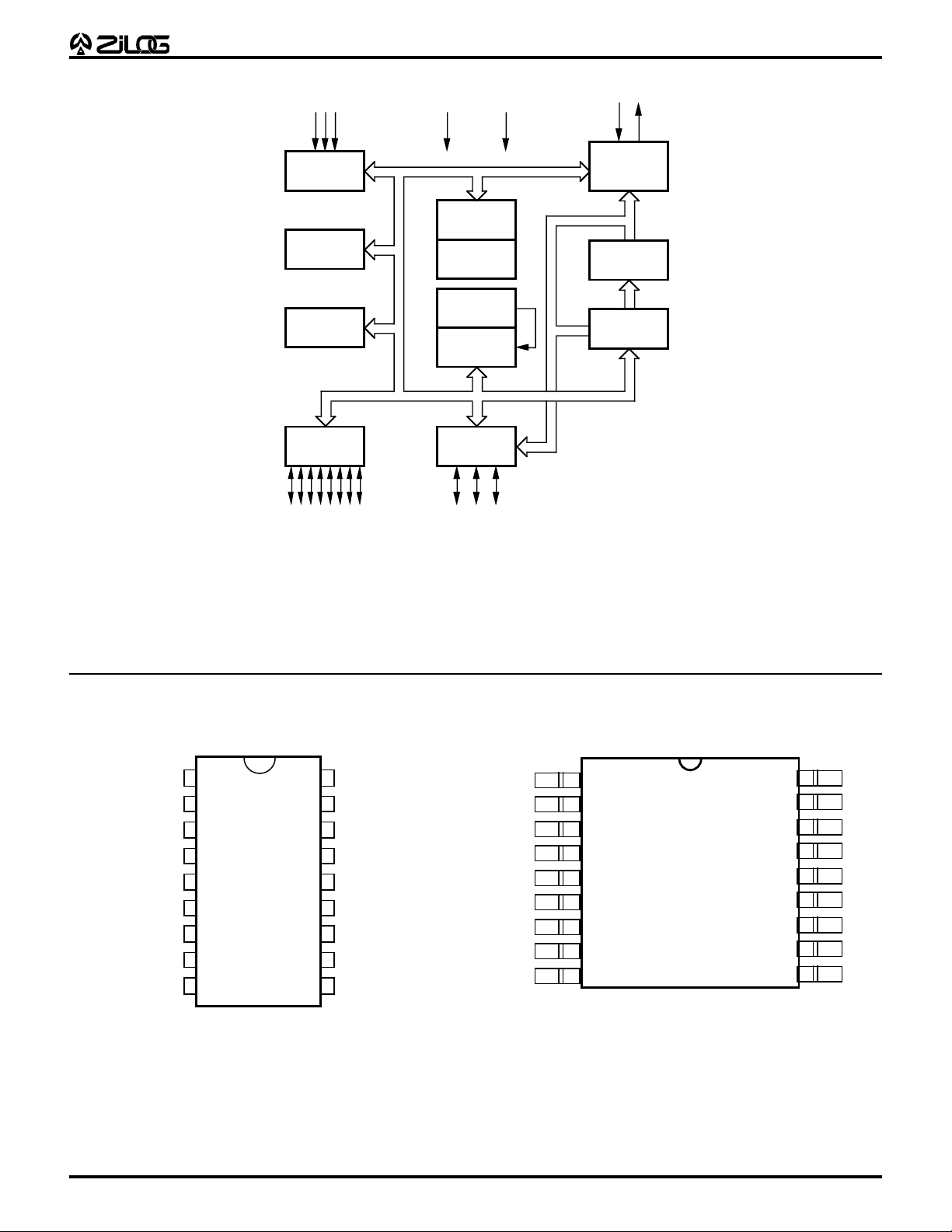
BLOCK DIAGRAM
Input
Port 3
Counter/
Timers (2)
Interrupt
Control
Port 2
I/O
(Bit Programmable)
VDD
ALU
FLAG
Register
Pointer
Register File
144 x 8-Bit
Port 0
I/O
VSS
XTAL
Machine
Timing & Inst.
Control
Prg. Memory
2048 x 8-Bit
Program
Counter
PIN DESCRIPTIONS
P24
P25
P26
P27
VDD
XTAL2
XTAL1
P31
P32
1
2
3
4
5
6
7
8
9
18
17
16
15
14
13
12
11
10
Functional Block Diagram
P23
P22
P21
P20
VSS
P02
P01
P00
P33
XTAL2
XTAL1
P24
P25
P26
P27
VDD
P31
P32
118
2
3
4
5
6
7
8
9
17
16
15
14
13
12
11
10
P23
P22
P21
P20
VSS
P02
P01
P00
P33
18-Pin DIP Configuration
18-Pin SOIC Configuration
2
Page 3
ABSOLUTE MAXIMUM RATINGS
PRELIMINARY
Z86217/C17
CP95KEY1000
Sym Parameter Min Max Units
V
T
T
Notes:
* Voltages on all pins with respect to GND
† See Ordering Information
DD
STG
A
Supply Voltage (*) –0.3 +7 V
Storage Temp –65° +150° C
Oper Ambient Temp † † C
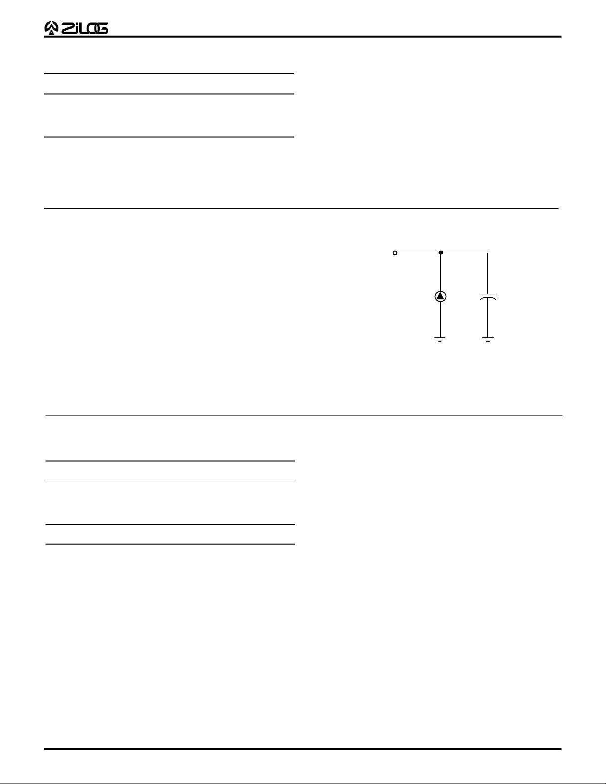
STANDARD TEST CONDITIONS
The characteristics listed below apply for standard test
conditions as noted. All voltages are referenced to GND.
Positive current flows into the referenced pin (Test Load).
Stress greater than those listed under Absolute Maximum
Ratings may cause permanent damage to the device. This
is a stress rating only; operation of the device at any
condition above those indicated in the operational sections of these specifications is not implied. Exposure to
absolute maximum rating conditions for extended periods
may affect device reliability.
From Output
Under Test
150 pFI
CAPACITANCE
TA = GND = 0V, f = 1.0 MHz, unmeasured pins to GND
Parameter Max
Input capacitance 10 pF
Output capacitance 20 pF
I/O capacitance 25 pF
Vdd SPECIFICATION
Vdd = 3.0V to 5.5V
Test Load Diagram
3
Page 4

PRELIMINARY
DC ELECTRICAL CHARACTERISTICS
TA = 0°C to +70°C Typical
Symbol Parameter V
Max Input Voltage 3.0V 12 V VIN = 250 µA
V
CH
Clock Input High 3.0V 0.7 V
Voltage Clock Generator
V
CL
Clock Input Low 3.0V VSS – 0.3 0.2 V
Voltage Clock Generator
V
IH
Input High Voltage 3.0V 0.7 V
Schmitt-Triggered 5.5V 0.7 V
V
IH
Input High Voltage 3.0V 0.7 V
CMOS Input 5.5V 0.7 V
V
IL
Input Low Voltage 3.0V VSS – 0.3 0.2 V
Schmitt-Triggered 5.5V VSS – 0.3 0.2 V
V
IL
Input Low Voltage 3.0V VSS – 0.3 0.2 V
CMOS Input 5.5V VSS – 0.3 0.2 V
V
OH
V
OL1
V
OL2
V
LV
Output High Voltge 3.0V V
Output Low Voltage 3.0V 0.4 0.13 V IOL = +4.0 mA
Output Low Voltage 3.0V 1.5 0.8 V IOL = 20.0 mA,
VCC Low Voltage 2.7 2.3 V @ 2 MHz Max
Protection Voltage
V
TP
Trip Point 3.0V 0.4 V
Voltage 5.5V
I
IL
I
OL
Input Leakage 3.0V –1.0 1.0 µAV
Output Leakage 3.0V –1.0 1.0 0.4 µAV
DD
5.5V 12 V VIN = 250 µA
5.5V 0.7 V
5.5V VSS – 0.3 0.2 V
5.5V VDD – 0.4 5.5 V IOH = –2.0 mA
5.5V 0.4 0.07 V IOL = +4.0 mA
5.5V 0.8 0.3 V IOL = 20.0 mA,
5.5V –1.0 1.0 0.4 µAV
5.5V –1.0 1.0 µAV
CP95KEY1000
Min Max @ 25°C Units Conditions
V
DD
DD
+ 0.3 2.0 V Driven by External
DD
V
+ 0.3 3.0 V Driven by External
DD
Clock Generator
DD
DD
0.8 V Driven by External
1.5 V Driven by External
Clock Generator
V
DD
DD
DD
DD
– 0.4 2.8 V IOH = –2.0 mA
DD
+ 0.3 1.6 V
DD
V
+ 0.3 2.6 V
DD
V
+ 0.3 1.4 V
DD
V
+ 0.3 2.6 V
DD
DD
DD
DD
DD
1.4 V
2.6 V
1.3 V
2.4 V
3 Pin Max
3 Pin Max
DD
V
= OV, V
IN
= OV, V
IN
= OV, V
IN
= OV, V
IN
Z86217/C17
CC
CC
CC
CC
Note:
For 2.75V operating, the device operates down to VLV. The minimum
operational VDD is determined on the value of the voltage VLV at the
ambient temperature. The VLV increases as the temperature decreases.
4
Page 5

TA = 0°C to +70°C Typical
Sym Parameter V
DD
PRELIMINARY
Min Max @ 25°C Units Conditions
Z86217/C17
CP95KEY1000
I
I
DD
DD1
Supply Current 3.0V 1.5 0.41 mA All Output and I/OPins
Floating @ 1 MHz
5.5V 3.0 1.44 mA All Output and I/O Pins
Floating @ 1 MHz
3.0V 2.0 0.93 mA All Output and I/O Pins
Floating @ 2 MHz
5.5V 4.0 2.60 mA All Output and I/O Pins
Floating @ 2 MHz
3.0V 3.0 1.64 mA All Output and I/O Pins
Floating @ 4 MHz
5.5V 6.0 4.28 mA All Output and I/O Pins
Floating @ 4 MHz
Standby Current 3.0V 0.6 0.15 mA HALT Mode VIN = 0V,
VCC @ 1 MHz
5.5V 1.3 0.70 mA HALT Mode VIN = 0V,
VCC @ 1 MHz
3.0V 0.8 0.20 mA HALT Mode VIN = 0V,
VCC @ 2 MHz
5.5V 1.5 0.80 mA HALT Mode VIN = 0V,
VCC @ 2 MHz
3.0V 1.0 0.3 mA HALT Mode VIN = 0V,
VCC @ 4 MHz
5.5V 2.0 1.0 mA HALT Mode VIN = 0V,
VCC @ 4 MHz
I
I
DD2
PU
Standby Current 3.0V 200 120 µA STOP Mode VIN = 0V,
Pull-Up Current
Port P20-P23 (100K) 3.0V –35 –13 µA
Port P24-P27* (20K) 3.0V –100 –58 µA
Port P00-P03 3.0V –35 –13 µA
Port P31, P33 5.5V –100 –56 µA
I
PD
Pull-Down Current 3.0V 80 40 µA
Port P32* (47K) 5.5V 250 160 µA
Note:
*Available on the Z86C17 only.
VCC WDT is Running
5.5V 200 120 µA STOP Mode VIN = 0V,
VCC WDT is Running
5.5V –100 –57 µA
5.5V –400 –270 µA
5
Page 6

PRELIMINARY
Z86217/C17
CP95KEY1000
AC ELECTRICAL CHARACTERISTICS
TA = 0°C to +70°C
1 MHz 4 MHz
No Symbol Parameter V
DD
1 TpC Input Clock Period 3.0V 1,000 100,000 250 100,000 ns [1]
5.5V 1,000 100,000 250 100,000 ns [1]
2 TrC,TfC Clock Input Rise 3.0V 25 25 ns [1]
and Fall Times 5.5V 25 25 ns
3 TwC Input Clock Width 3.0V 475 100 ns [1]
5.5V 475 100 ns [1]
4 TwTinL Timer Input Low Width 3.0V 100 100 ns [1]
5.5V 70 70 ns [1]
5 TwTinH Timer Input High Width 3.0V 2.5TpC 2.5TpC [1]
5.5V 2.5TpC 2.5TpC [1]
6 TpTin Timer Input Period 3.0V 4TpC 4TpC [1]
5.5V 4TpC 4TpC [1]
Min Max Min Max Units Notes
7 TrTin, Timer Input Rise 3.0V 100 100 ns [1]
TtTin and Fall Timer 5.5V 100 100 ns [1]
8 TwIL Int. Request Input 3.0V 100 100 ns [1,2]
Low Time 5.5V 70 70 ns [1,2]
9 TwIH Int. Request Input 3.0V 2.5TpC 2.5TpC [1]
High Time 5.5V 2.5TpC 2.5TpC [1,2]
10 Twdt Watch-Dog Timer 3.0V 25 25 ms [1]
Time Out Timer 5.5V 10 10 ms [1]
11 T
POR
Power-On Reset 3.0V 6 6 ms [1]
Time 5.5V 2 2 ms [1]
Notes:
[1] Timing Reference uses 0.9 VDD for a logic 1 and 0.1 VDD for a logic 0.
[2] Interrupt request through Port 3 (P33-P31)
6
Page 7

TIMING DIAGRAM
Clock
T
IN
7 7
PRELIMINARY
1
2 2 3
3
Z86217/C17
CP95KEY1000
IRQ
4
N
8
5
6
9
Electrical Timing Diagram
Low Margin:
Customer is advised that this product does not meet
Zilog’s internal guardbanded test policies for the specification requested and is supplied on an exception basis.
Customer is cautioned that delivery may be uncertain and
that, in addition to all other limitations on Zilog liability
Pre-Characterization Product:
The product represented by this CPS is newly introduced
and Zilog has not completed the full characterization of the
product. The CPS states what Zilog knows about this
product at this time, but additional features or non-con-
stated on the front and back of the acknowledgement,
Zilog makes no claim as to quality and reliability under the
CPS. The product remains subject to standard warranty for
replacement due to defects in materials and workmanship.
formance with some aspects of the CPS may be found,
either by Zilog or its customers in the course of further
application and characterization work. In addition, Zilog
cautions that delivery may be uncertain at times, due to
start-up yield issues.
© 1995 by Zilog, Inc. All rights reserved. No part of this document
may be copied or reproduced in any form or by any means
without the prior written consent of Zilog, Inc. The information in
this document is subject to change without notice. Devices sold
by Zilog, Inc. are covered by warranty and patent indemnification
provisions appearing in Zilog, Inc. Terms and Conditions of Sale
only. Zilog, Inc. makes no warranty, express, statutory, implied or
by description, regarding the information set forth herein or
regarding the freedom of the described devices from intellectual
property infringement. Zilog, Inc. makes no warranty of merchantability or fitness for any purpose. Zilog, Inc. shall not be
responsible for any errors that may appear in this document.
Zilog, Inc. makes no commitment to update or keep current the
information contained in this document.
Zilog’s products are not authorized for use as critical components in life support devices or systems unless a specific written
agreement pertaining to such intended use is executed between
the customer and Zilog prior to use. Life support devices or
systems are those which are intended for surgical implantation
into the body, or which sustains life whose failure to perform,
when properly used in accordance with instructions for use
provided in the labeling, can be reasonably expected to result in
significant injury to the user.
Zilog, Inc. 210 East Hacienda Ave.
Campbell, CA 95008-6600
Telephone (408) 370-8000
Telex 910-338-7621
FAX 408 370-8056
Internet: http://www.zilog.com
7
 Loading...