

Page 1
FEATURES
PRELIMINARY
PRELIMINARY
CUSTOMER PRODUCT SPECIFICATION
Z86160
SET-TOP CONTROLLER
Z86160
CP96TEL1700
ROM RAM* Package
Part Kbytes Bytes Speed Information
Z86160 32 768 16 100-Pin QFP
*General-Purpose
n 3.0- to 5.5-Volt Operating Range
n Low-Power Consumption
n Custom Input/Output Lines
GENERAL DESCRIPTION
The Z86160 is a member of the Z8® single-chip
microcontroller family offering a unique architecture that is
characterized by Zilog's 8-bit microcontroller core.
This CMOS microcontroller features fast execution,
efficient use of memory, sophisticated interrupts, input/
output bit manipulation capabilities, and easy hardware/
software system expansion along with low-cost and
low-power consumption.
For applications demanding powerful I/O capabilities, the
Z86160 fulfills this with custom I/O, specifically tailored to
meet the needs of set-top requirements.
Four basic address spaces, the Program Memory, Data
Memory, 236 General-Purpose Registers, and 512 bytes
of protected RAM, support a wide range of memory
configurations. The protected RAM is mapped into data
memory.
n 0°C to +70°C Temperature Range
n 512 Bytes Battery Backed-Up (BBU) Secure RAM
n Keypad Buffer
n LED Controller
n Two Comparators
n Two On-Chip Counter/Timers
To unburden the program from coping with real-time
problems such as counting/timing, and serial data communications, the Z86160 offers two on-chip counter/timers
with a large number of user selectable modes, and an
asynchronous receiver/transmitter (UART) (see Block
Diagram).
Notes:
All Signals with a preceding front slash, "/", are active Low, e.g.,
B//W (WORD is active Low); /B/W (BYTE is active Low, only).
Power connections follow conventional descriptions below:
Connection Circuit Device
Power V
Ground GND V
CC
V
DD
SS
CP96TEL1700 (3/96)
1
Page 2
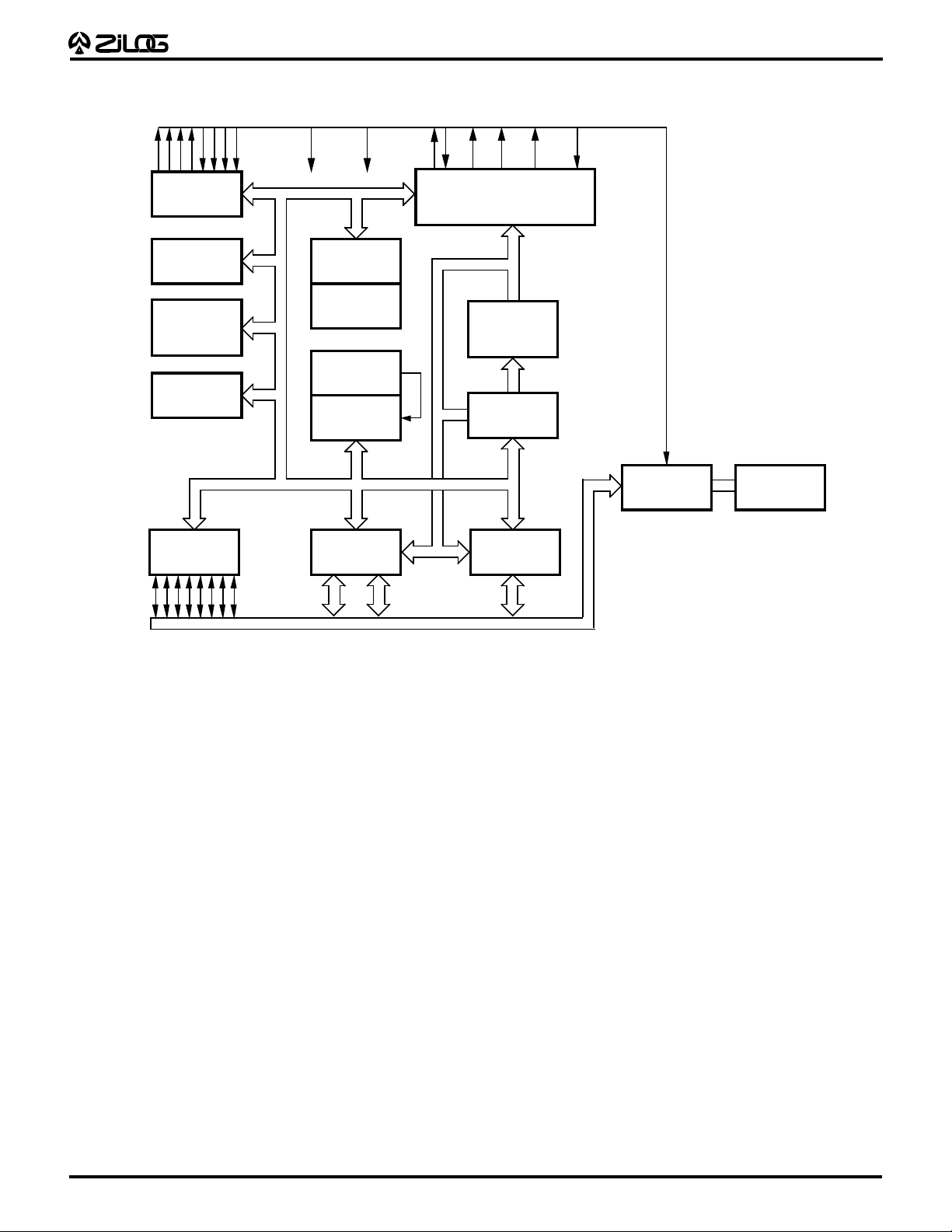
GENERAL DESCRIPTION
Output Input
Vcc GND
PRELIMINARY
XTAL
/AS /DS R//W /RESET
Z86160
CP96TEL1700
Port 3
UART
Counter/
Timers
(2)
Interrupt
Control
Port 2
I/O
(Bit Programmable)
ALU
FLAGS
Register
Pointer
Register File
256 x 8-Bit
Port 0
44
Address or I/O
(Nibble Programmable)
Machine Timing and
Instruction Control
Prg. Memory
32,768
x 8-Bit
Program
Counter
Port 1
8
Address/Data or I/O
(Byte Programmable)
Custom
Logic
I/O
Secure
RAM
512 Bytes
Figure 1. Z86160 Functional Block Diagram
2
Page 3
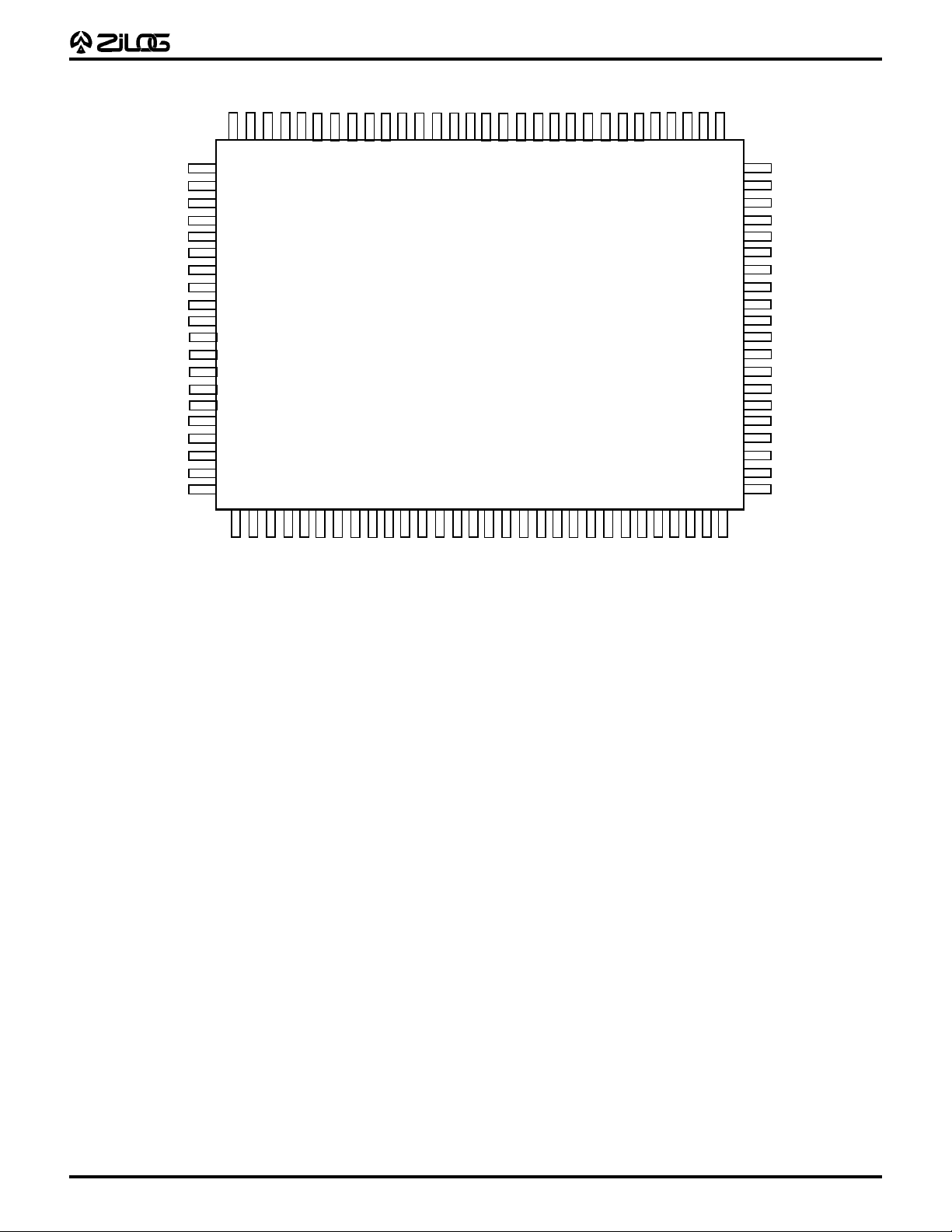
PIN DESCRIPTION
PRELIMINARY
Z86160
CP96TEL1700
81
100
80
51
50
Z86160
QFP
31
1
Figure 2. Z86160 100-Pin QFP Package
30
3
Page 4

PIN DESCRIPTION (Continued)
PRELIMINARY
Z86160 100-Pin QFP Pin Identification
Z86160
CP96TEL1700
Pin # Symbol
1 EXADR14
2 EXR/W
3 EXADR07
4 EXADR12
5 GND
6 EXADR13
7 EXADR08
8 EXADR06
9 EXADR09
10 V
CC
11 EXADR05
12 EXADR11
13 EXADR04
14 /EXDS
1 5 GND
16 EXADR03
17 EXADR10
18 EXADR02
19 /EXRAMCS
20 EXADR01
Pin # Symbol
26 V
CC
27 D5
28 D1
29 D4
30 D2
31 D3
32 S0
33 S1
3 4 GND0
3 5 GND1
3 6 GND2
3 7 GND3
38 S2
3 9 GND
40 I0
41 I1
42 I2
43 I3
44 I4
45 I5
Pin # Symbol
51 S4
52 S5
53 S6
54 K1
55 S7
56 T0
57 T1
58 T2
59 T3
60 T4
61 T5
6 2 GND
63 T6
64 T7
65 M0
66 M1
67 M2
68 V
CC
69 M3
70 K2
Pin # Symbol
76 M7
7 7 ON/OFF
7 8 GND
79 N1
80 N2
81 V
CC
82 K5
83 N3
84 K6
85 K7
86 L0
87 L1
88 L3
89 B0
90 B1
9 1 GND
92 XTAL1
93 XTAL2
9 4 GND
95 B2
21 D7
22 EXADR00
23 D6
24 D0
2 5 GND
46 I6
47 I7
48 K0
49 V
50 S3
71 M4
72 K3
73 M5
CC
74 K4
75 M6
96 B3
97 L4
98 N4
99 N5
100 L5
4
Page 5

ABSOLUTE MAXIMUM RATINGS
PRELIMINARY
Z86160
CP96TEL1700
Symbol Description Min Max Units
V
CC
T
STG
T
A
Notes:
* Voltages on all pins with respect to GND.
Supply Voltage* –0.3 +7.0 V
Storage Temp –65 +150 C
Oper Ambient Temp 0° 70° C
STANDARD TEST CONDITIONS
The characteristics listed below apply for standard test
conditions as noted. All voltages are referenced to GND.
Positive current flows into the referenced pin (Test Load).
Stresses greater than those listed under Absolute Maximum Ratings may cause permanent damage to the device. This is a stress rating only; operation of the device at
any condition above those indicated in the operational
sections of these specifications is not implied. Exposure to
absolute maximum rating conditions for an extended period may affect device reliability.
From Output
Under Test
I
15 pF
Figure 3. Test Load Diagram
5
Page 6

PRELIMINARY
DC ELECTRICAL CHARACTERISTICS
Z86160
TA = 0°C Typical
to +70°Cat
Sym Parameter Min Max 25°C Units Conditions
Z86160
CP96TEL1700
Max Input Voltage V
V
Clock Input High Voltage 0.85 V
CH
V
Clock Input Low Voltage V
CL
V
Input High Voltage 2 V
IH
V
Input Low Voltage V
IL
V
Output High Voltage 4 V I
O H
V
Output High Voltage V
O H
V
Output Low Voltage 0.75 V IOL = +7.0 mA [3]
O L
V
Output Low Voltage 0.3 V IOL = +2.0 mA [3]
O L
V
Output Low Voltage 0.3 V IOL = +1.0 mA [2]
O L
I
Input Leakage –2 2 µ AVIN = 0 V, V
IL
I
Output Leakage –2 2 µAVIN = 0 V, V
OL
I
Supply Current (Standard Mode) 44 30 mA [1] @ 16 MHz
CC
I
Standby Current (Standard Mode) 18.75 5.75 mA [1] HALT Mode VIN = 0 V, V
CC1
I
Standby Current 5 µA [1] @ 0 MHz VIN = 0 V, V
CC2
I
Auto Latch Low Current –14 14 5 µA
ALL
Notes:
[1] All inputs driven to either 0V or VCC, outputs floating.
[2] VCC = 3.0V to 3.6V
[3] VCC = 4.5V to 5.5V
Data Retention @ 2.0V – BBU
CCVCC
– 0.3 0.8 V Driven by External Clock Generator
SS
– 0.3 0.2 V
SS
+ 0.3 V IIN < 250 µA
CC
+ 0.3 V Driven by External Clock Generator
+ 0.3 V
CC
CC
– 100 mV V IOH = –100 µA
CC
V
= –2.0 mA [3]
OH
CC
CC
@ 16 MHz
CC
= 3V
CC
6
Page 7

AC CHARACTERISTICS
C
Additional Timing Diagram
lock
AC CHARACTERISTICS
Additional Timing Table
Z86160
PRELIMINARY
1 3
2 2 3
Additional Timing
Z86160
CP96TEL1700
TA = 0°C
to +70°C
16 MHz
No Symbol Parameter Min Max Units Notes
1 TpC Input Clock Period TBD ns [1]
2 TrC,TfC Clock Input Rise & Fall Times TBD n s [1]
3 TwC Input Clock Width TBD ns [1]
Notes:
[1] Clock timing references use 0.85VCC for a logic 1 and 0.8V for a logic 0.
7
Page 8

PRELIMINARY
LIMITATIONS
Be advised that AC Electrical Characteristics and Timing
Diagram information was unavailable at the time of this
publication, they will be supplied at a later date.
Development Projects:
Customer is cautioned that while reasonable efforts will be
employed to meet performance objectives and milestone
dates, development is subject to unanticipated problems
Z86160
CP96TEL1700
and delays. No production release is authorized or
committed until the Customer and Zilog have agreed upon
a Customer Procurement Specification for this project.
Low Margin:
Customer is advised that this product does not meet
Zilog's internal guardbanded test policies for the specification requested and is supplied on an exception basis.
Customer is cautioned that delivery may be uncertain and
that, in addition to all other limitations on Zilog liability
Pre-Characterization Product:
The product represented by this CPS is newly introduced
and Zilog has not completed the full characterization of the
product. The CPS states what Zilog knows about this
product at this time, but additional features or nonconformance with some aspects of the CPS may be found,
© 1996 by Zilog, Inc. All rights reserved. No part of this document
may be copied or reproduced in any form or by any means
without the prior written consent of Zilog, Inc. The information in
this document is subject to change without notice. Devices sold
by Zilog, Inc. are covered by warranty and patent indemnification
provisions appearing in Zilog, Inc. Terms and Conditions of Sale
only. Zilog, Inc. makes no warranty, express, statutory, implied or
by description, regarding the information set forth herein or
regarding the freedom of the described devices from intellectual
property infringement. Zilog, Inc. makes no warranty of merchantability or fitness for any purpose. Zilog, Inc. shall not be
responsible for any errors that may appear in this document.
Zilog, Inc. makes no commitment to update or keep current the
information contained in this document.
stated on the front and back of the acknowledgement,
Zilog makes no claim as to quality and reliability under
the CPS. The product remains subject to standard
warranty for replacement due to defects in materials and
workmanship.
either by Zilog or its customers in the course of further
application and characterization work. In addition, Zilog
cautions that delivery may be uncertain at times, due to
start-up yield issues.
Zilog’s products are not authorized for use as critical components in life support devices or systems unless a specific written
agreement pertaining to such intended use is executed between
the customer and Zilog prior to use. Life support devices or
systems are those which are intended for surgical implantation
into the body, or which sustains life whose failure to perform,
when properly used in accordance with instructions for use
provided in the labeling, can be reasonably expected to result in
significant injury to the user.
Zilog, Inc. 210 East Hacienda Ave.
Campbell, CA 95008-6600
Telephone (408) 370-8000
FAX 408 370-8056
Internet: http//:www.zilog.com
8
 Loading...