

Page 1

1
Z08617 NMOS Z8
®
8-BIT MCU
KEYBOARD CONTROLLER
FEATURES
C
USTOMER PROCUREMENT
S
PECIFICA TION
■ Low Power Consumption - 750 mW
■ 32 Input/Output Lines
■ Digital Inputs NMOS Levels with
Internal Pull-Up Resistors
■ 4 Kbytes ROM
■ Four Direct Connect LED Drive Pins
■ 124 Bytes of RAM
■ Hardware Watch-Dog Timer (WDT)
■ Two Programmable 8-Bit Counter/Timers,
Each with 6-Bit Programmable Prescaler
■ Six Vectored, Priority Interrupts from
Six Different Sources
■ On-Chip RC Oscillator
■ Clock Frequency: Up to 5MHz
■ Low EMI Emission
GENERAL DESCRIPTION
The Z08617 Keyboard Controller is a member of the
Z8® single-chip microcontroller family with 4 Kbytes
of ROM. The device is housed in a 40-pin DIP package,
and is manufactured in NMOS technology. The Z08617
microcontroller offers fast execution, efficient use of
memory, sophisticated interrupt, input/output bitmanipulation capabilities, and easy hardware/software system expansion along with low cost and low
power consumption.
The Z08617 architecture is characterized by a flexible I/O scheme, an efficient register, I/O, and a
number of ancillary features that are useful in many
industrial and advanced scientific applications.
For applications which demand powerful I/O capabilities, the Z08617 provides 32 pins dedicated to input
and output. These lines are grouped into four ports,
each port consists of 8 lines, and are configurable
under software control to provide timing, status
signals, and serial or parallel I/O ports.
The Z08617 offers low EMI emission which is achieved
by means of several modifications in the output
drivers and clock circuitry of the device.
There are two basic address spaces which are available to support this wide range of configurations:
Program Memory and 124 General-Purpose Registers.
The Z08617 offers two on-chip counter/timers with
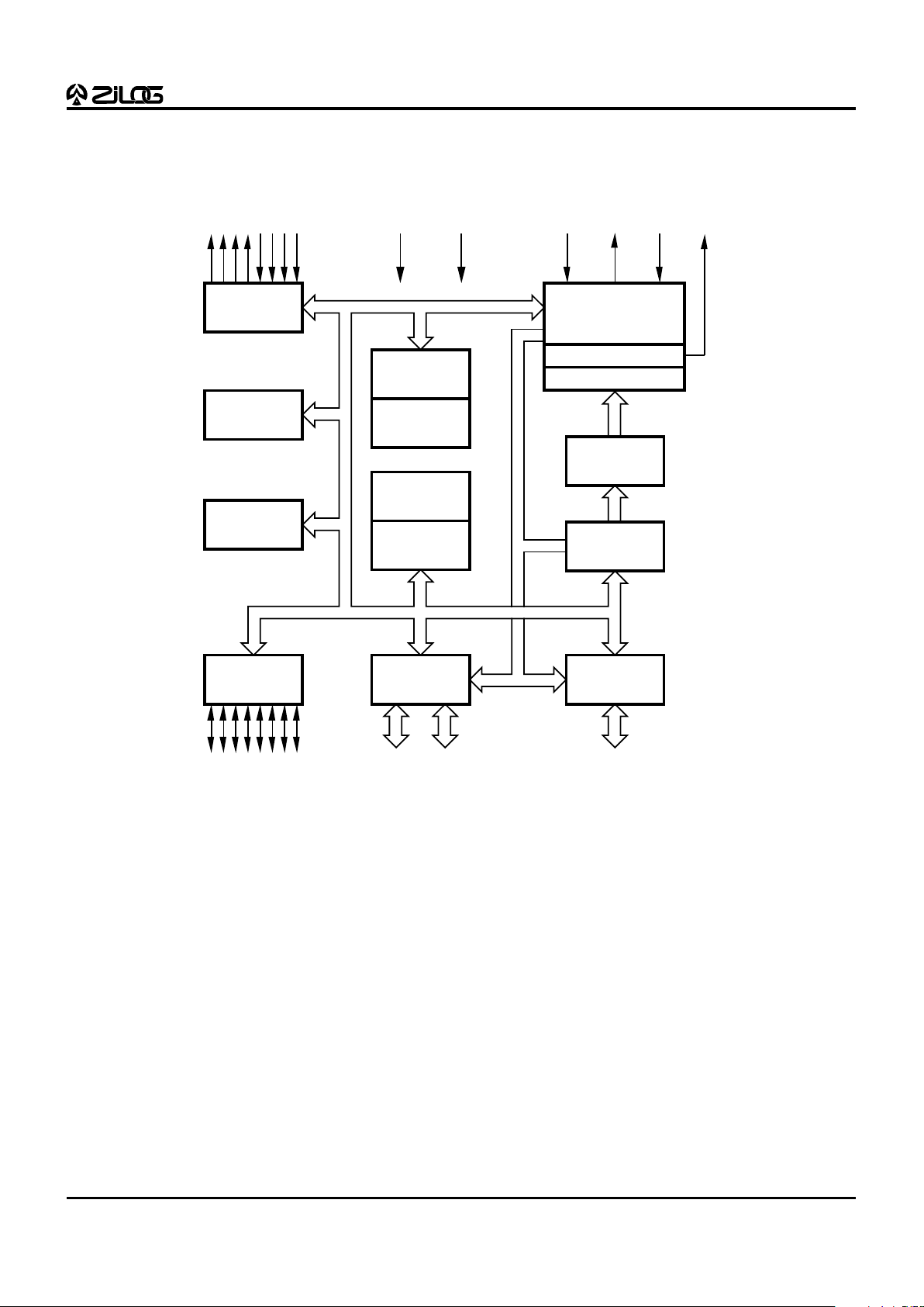
a large number of user-selectable modes. This unburdens the program from coping with real-time problems such as counting/timing (Figure 1).
Notes:
All Signals with a preceding front slash, "/", are active Low,
e.g., B//W (WORD is active Low); /B/W (BYTE is active Low,
only).
Power connections follow conventional descriptions below:
Connection Circuit Device
Power V
CC
V
DD
Ground GND V
SS
DS96KEY0300
Z08617
NMOS Z8® 8-BIT MCU
KEYBOARD CONTROLLER
Page 2
Z08617 NMOS Z8
®
8-BIT MCU
KEYBOARD CONTROLLER
2
GENERAL DESCRIPTION (Continued)
Port 3
Counter/
Timers (2)
Interrupt
Control
Port 2
I/O
(Bit Programmable)
ALU
Flags
Register
Pointer
Register File
124 x 8-Bit
Machine Timing
& Instruction Control
Program
Memory
Program
Counter
Vcc GND
Output Input
Port 0 Port 1
I/O
Output Open-Drain
(Nibble Programmable)
I/O
Output Open-Drain
(Byte Programmable)
44 8
WDT
POR
/WDTOUT
/RESET
XTAL2
XTAL1
Figure 1. Z08617 Functional Block Diagram
Page 3
3
Z08617 NMOS Z8
®
8-BIT MCU
KEYBOARD CONTROLLER
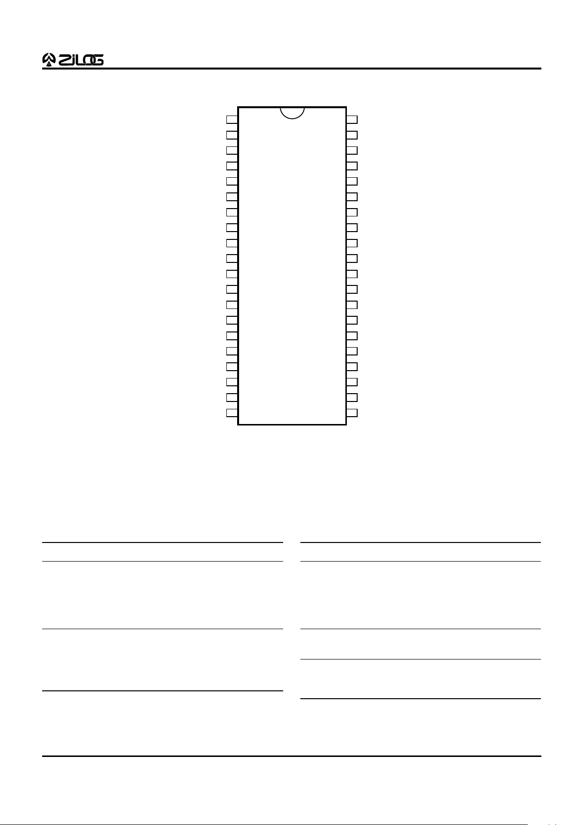
PIN IDENTIFICATION
Figure 2. 40-Pin DIP Pin Configuration
Pin # Symbol Function Direction
1V
CC
Power Supply Input
2 CLK Out Clock Out Output
3 RC In Z8 Clock Input
4 P37 Port 3, Pin 7 Output
5 P30 Port 3, Pin 0 Input
6 /RESET Reset Input
*7 GND Ground
*8 N/C Not Connected
9 /WDTOUT Watch-Dog Timer Output
10 P35 Port 3, Pin 5 Output
Pin # Symbol Function Direction
11 GND Ground
12 P32 Port 3, Pin 2 Input
13-20 P07-P00 Port 0, Pins 0,1,2,3,4,5,6,7 In/Output
21-28 P17-P10 Port 1, Pins 0,1,2,3,4,5,6,7 In/Output
29 P34 Port 3, Pin 4 Output
30 P33 Port 3, Pin 3 Input
31-38 P27-P20 Port 2, Pins 0,1,2,3,4,5,6,7 In/Output
34-38 P24-P20 Port 2, Pins 0, 1, 2, 3, 4 In/Output
39 P31 Port 3, Pin 1 Input
40 P36 Port 3, Pin 6 Output
Table 1. 40-Pin DIP Pin Identification
1
2
3
4
5
6
7
8
9
10
11
12
13
14
15
16
17
18
19
20
VCC
CLK Out
RC In
P37
P30
/RESET
*GND
*N/C
/WDTOUT
P35
GND
P32
P00
P01
P02
P03
P04
P05
P06
P07
P36
P31
P27
P26
P25
P24
P23
P22
P21
P20
P33
P34
P17
P16
P15
P14
P13
P12
P11
P10
40
39
38
37
36
35
34
33
32
31
30
29
28
27
26
25
24
23
22
21
Z08617
DIP
Note:
* Pin 8 is connected to the chip, although used only for testing.
This pin
must
float. Pin 7 is a test pin and
must
be grounded.
Page 4
Z08617 NMOS Z8
®
8-BIT MCU
KEYBOARD CONTROLLER
4
ABSOLUTE MAXIMUM RATINGS
Symbol Description Min Max Units
V
CC
Supply Voltage* –0.3 +7.0 V
T
STG
Storage Temp –65 +150 C
T
A
Oper Ambient Temp † †
Notes:
* Voltage on all pins with respect to GND.
† See ordering information
Stresses greater than those listed under Absolute
Maximum Ratings may cause permanent damage to
the device. This is a stress rating only; operation of the
device at any condition above those indicated in the
operational sections of these specifications is not
implied. Exposure to absolute maximum rating conditions for extended periods may affect device reliability.
STANDARD TEST CONDITIONS
The characteristics listed here apply for standard test
conditions as noted. All voltages are referenced to
GND. Positive current flows into the referenced pin
(Figure 17).
From Output
Under Test
150 pF
Figure 17. Test Load Diagram
STANDARD TEST CONDITIONS
T
A
= 25°C, VCC = GND = 0V, f = 1.0 MHz, unmeasured pins returned to ground.
Parameter Max
Input capacitance 12 pF
Output capacitance 12 pF
I/O capacitance 12 pF
Page 5
5
Z08617 NMOS Z8
®
8-BIT MCU
KEYBOARD CONTROLLER
DC CHARACTERISTICS
VCC = 4.75V to 5.25V @ 0°C to -55°C
Sym Parameter Min Max Typ* Unit Condition
V
IH
Input High Voltage 2.0 V
CC
V
V
IL
Input Low Voltage –0.3 0.8 V
V
RH
Reset Input High Voltage 3.8 V
CC
V
V
RL
Reset Input Low Voltage –0.3 0.8 V
V
OH
Output High Voltage 2.0 V IOH = –250 µA (Port 2 only)
Output High Voltage 2.4 V IOH = –250 µA (Port 3 only)
V
OL
Output Low Voltage 0.8 V IOL = 10.0 mA (See note [1] below.)
I
IL
Input Leakage –10 10 µAVIN = 0V, 5.25V (See note [3] below.)
I
OL
Output Leakage –10 10 µAVIN = 0V, 5.25V (See note [2] below.)
I
IR
Reset Input Current –335 –775 –477 µAV
IN
= 0V, 5.25V
I
R1
Input Current –335 –775 µA Pull-up resistor=10.4 Kohms, VIN=0.0V
I
R2
Input Current –1.6 –2.9 mA Pull-up resistor = 2.4 Kohms, VIN=0.0V
I
CC
VCC Supply Current 160 mA
WDT Watch-Dog Timer 2.0 mA VOL=0.4 Volt
Notes:
* Typical @ 25°C
[ 1 ] Ports P37-P34 may be used to sink 12 mA. These may be used
for LEDs or as general-purpose outputs requiring high sink
current.
[ 2 ] P00-P07, P10-P17, P20-P25, P30-P33 as output mode open-
drain as a logic one.
[ 3 ] P00-P07, P10-P17, P20-P25, P30-P33 as output mode open-
drain as a logic one.
Page 6
Z08617 NMOS Z8
®
8-BIT MCU
KEYBOARD CONTROLLER
6
PIN FUNCTIONS
RCIN This pin is connected between a precision resistor
on the power supply from the precision RC Oscillator.
CLK Out This pin is the syste m clock of the Z8 and
runs at the frequency of the RC Oscillator. Any load on
this pin will effect the RC Oscillator frequency.
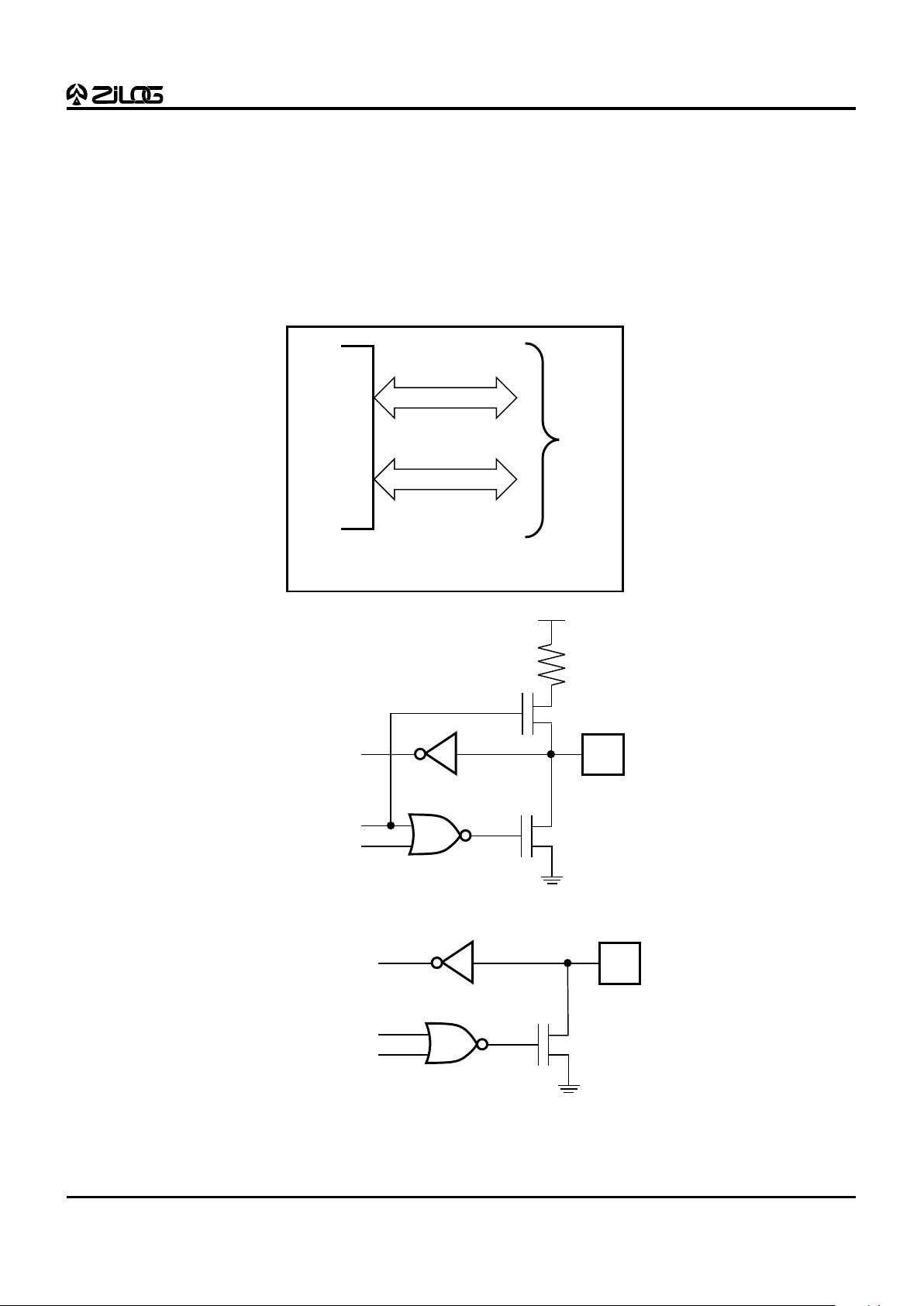
Port 0 (P07-P00). Port 0 is an 8-bit, nibble programmable, bi-directional, NMOS compatible I/O port. These
eight I/O lines can be configured under software
control as a nibble input port, or as a nibble open-drain
output port. When used as an I/O port, inputs are
standard NMOS (Figure 5). Port P03-P00 has 10.4
Kohms (±35%) pull-up resistors when configured as
inputs.
Figure 5. Port 0 Configuration
Port 0
I/O
(Open-Drain Output)
Z8615
4
4
Input
Output
Pad
OEN
10.4 Kohms
(a) Port P00-P03
Input
Output
Pad
OEN
(b) Port P04-P07
Page 7
7
Z08617 NMOS Z8
®
8-BIT MCU
KEYBOARD CONTROLLER
PIN FUNCTIONS (Continued)
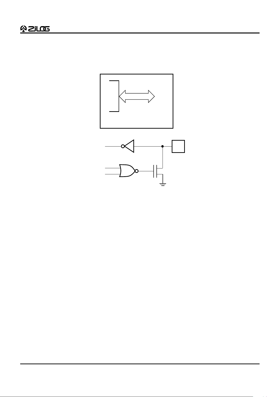
Port 1 (P17-P10). Port 1 is an 8-bit, byte programmable,
bidirectional, NMOS compatible I/O port. These eight I/O
lines are configured under software control program as a
byte input port or as an open-drain output port. When used
as an I/O port, inputs are standard NMOS (Figure 6).
Port 1
I/O
(Open-Drain Output)
Z8615 8
Input
Output
Pad
OEN
Figure 6. Port 1 Configuration
Page 8
Z08617 NMOS Z8
®
8-BIT MCU
KEYBOARD CONTROLLER
8
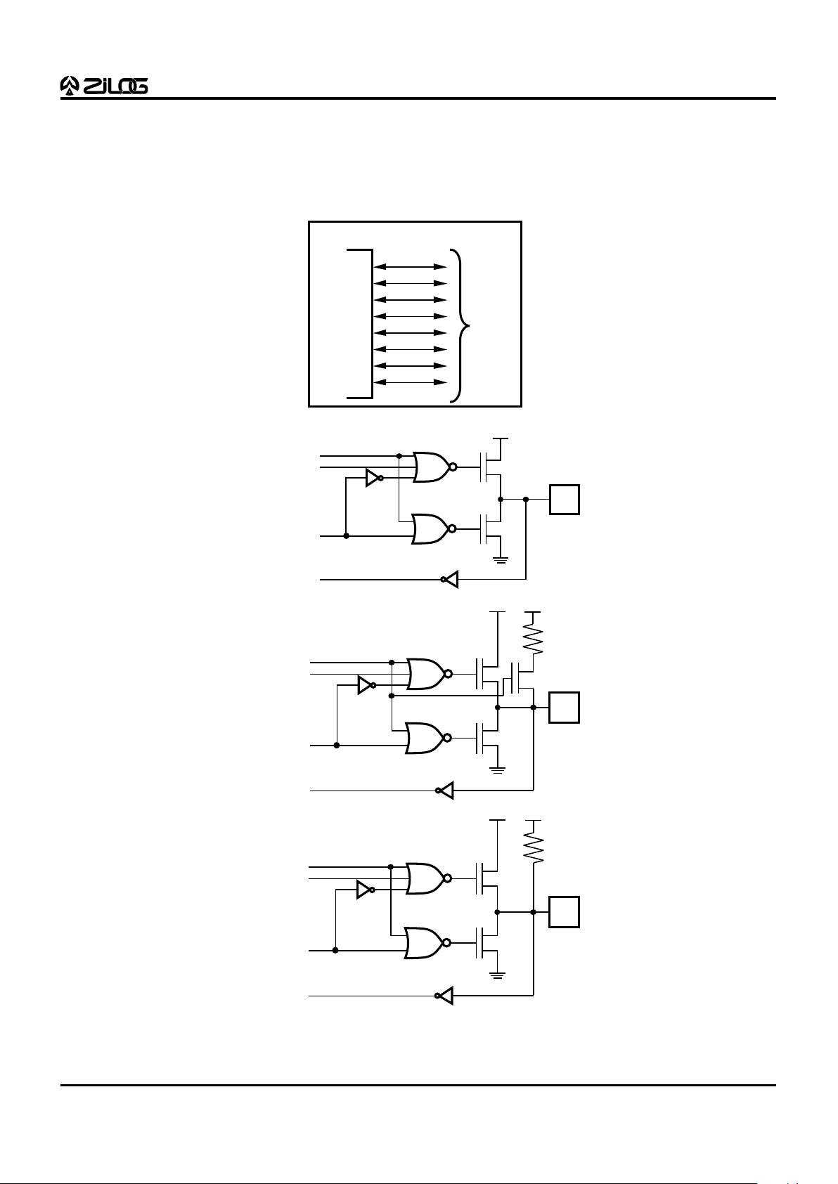
Port 2 (P27-P20). Port 2 is an 8-bit, bit programmable, bidirectional, NMOS compatible I/O port. These eight I/O
lines are configured under the software control program
for I/O. Port 2 can be programmed as bit-by-bit independently, as input or output, or configured to provide open-
drain outputs (Figure 7). P26 and P27 have 2.4 Kohms
(± 25%) pull-up resistors and are capable of sourcing
2.4 mA. P24 and P25 have 10.4 Kohms (± 35%) pull-up
when configured as inputs.
Open-Drain
OUT
OEN
IN
Pad
Input
(a) Ports P20-P23
Port 2
(I/O)
Z8615
Open-Drain
OUT
OEN
IN
Pad
10.4 Kohms
Input
(b) Ports P24-P25
Open-Drain
OUT
OEN
IN
Pad
2.4 Kohms
Input
(c) Ports P26-P27
Figure 7. Port 2 Configuration
Page 9

9
Z08617 NMOS Z8
®
8-BIT MCU
KEYBOARD CONTROLLER
PIN FUNCTIONS (Continued)
Port 3 (P37-P30). Port 3 is an 8-bit, NMOS compatible four-
fixed-input and four-fixed-output I/O port. These eight I/O
lines have four-fixed-input (P33-P30) and four-fixed-output (P37-P34) ports. Port 3 inputs have 10.4 Kohms (±35%)
pull-up resistors and port 3 outputs are capable of driving
up to four LEDs.
Port 3 is configured under software control to provide
the following control functions: four external interrupt
request signals (IRQ3-IRQ0); timer input and output
signals (TIN and T
OUT
- Figure 8).
/RESET (input, active Low). When activated, /RESET
initializes the Z08617. When /RESET is deactivated,
program execution begins from the internal program
location at 000CH. Reset pin has a 10.4 Kohms pullup resistor. Once this pin is pulled Low, it takes about
150 ms for microcon-troller initialization.
Figure 8. Port 3 Configuration
Port 3
(I/O or
Control)
Z8615
Input
Pad
Output
Pad
(a) Port 3 P34-P37
(b) Port 3 P30-P33
10.4 Kohms
Page 10

Z08617 NMOS Z8
®
8-BIT MCU
KEYBOARD CONTROLLER
10
FUNCTIONAL DESCRIPTION
The device incorporates special functions to enhance
Zilog's Z8 applications as a keyboard controller, scientific research and advanced technologies applications.
Program Memory. The 16-bit program counter addresses 4 Kbytes of program memory space at internal locations (Figure 9).
The first 12 bytes of program memory are reserved for the
interrupt vectors. These locations have six 16-bit vectors
that correspond to the six available interrupts.
Byte 12 to byte 4095 consists of on-chip, mask
programmed ROM. Addresses 4096 and greater are
reserved.
12
11
10
9
8
7
6
5
4
3
2
1
0
On-Chip
ROM
Location of
First Byte of
Instruction
Executed
After RESET
Interrupt
Vector
(Lower Byte)
Interrupt
Vector
(Upper Byte)
IRQ5
IRQ4
IRQ4
IRQ3
IRQ3
IRQ2
IRQ2
IRQ1
IRQ1
IRQ0
IRQ0
IRQ5
65535
4096
4095
Reserved
Figure 9. Program Memory Map
Page 11

11
Z08617 NMOS Z8
®
8-BIT MCU
KEYBOARD CONTROLLER
FUNCTIONAL DESCRIPTION (Continued)
Register File. The register file (Figure 10) consists of four
I/O port registers, 124 general-purpose registers and 16
control and status registers (R3-R0, R127-R4, and R255R240, respectively). The instructions can access registers
directly or indirectly through an 8-bit address field. This
allows short, 4-bit register addressing using the Register
Pointer (Figure 11). In the 4-bit mode, the register file is
divided into nine working-register groups, each occupying 16 continuous locations. The Register Pointer addresses the starting location of the active working-register
group.
Figure 10. Register File Configuration
Figure 11. Register Pointer Configuration
Stack Pointer (Bits 7-0)
R255
General-Purpose Register (Bits 7-0)
Register Pointer
Program Control Flags
Interrupt Mask Register
Interrupt Request Register
Interrupt Priority Register
Ports 1-0 Mode
Port 3 Mode
Port 2 Mode
T0 Prescaler
Timer/Counter0
T1 Prescaler
Timer/Counter1
Timer Mode
Reserved
Not Implemented
General-Purpose
Registers
Port 3
Port 2
Port 1
Port 0
R254
R253
R252
R251
R250
R249
R248
R247
R246
R245
R244
R243
R242
R241
R240
R127
R3
R2
R1
R0
SPL
GPR
RP
FLAGS
IMR
IRQ
IPR
P01M
P3M
P2M
PREQ
T0
PRE1
T1
TMR
P3
P2
P1
P0
R4
LOCATION IDENTIFIERS
The upper nibble of the register file address
provided by the register pointer specifies
the active working-register group.
r7 r6 r5 r4 R253
(Register Pointer)
I/O Ports
Specified Working
Register Group
The lower nibble
of the register
file address
provided by the
instruction points
to the specified
register.
r3 r2 r1 r0
Register Group 1
Register Group 0
R15 to R0
Register Group F
R15 to R4
R3 to R0
R15 to R0
•
•
•
•
•
FF
F0
0F
00
1F
10
2F
20
•
•
•
•
•
•
•
•
•
Page 12

Z08617 NMOS Z8
®
8-BIT MCU
KEYBOARD CONTROLLER
12
Stack. The Z08617 internal register files are used for the
stack. An 8-bit Stack Pointer (R255) is used for the internal
stack that resides within the 124 general-purpose registers.
Counter/Timers. There are two 8-bit programmable
counter/timers (T0-T1), each driven by its own 6-bit
programmable prescaler. The T1 prescaler can be
driven by internal or external clock sources, however,
the T0 prescaler is driven by the internal clock only
(Figure 12).
The 6-bit prescalers can further divide the input
frequency of the clock source by any integer number
from 1 to 64. Each prescaler drives its own counter,
which decrements the value (1 to 256) that has been
loaded into the counter. When both the counter and
prescaler reach the end of count, a timer interrupt
request, IRQ4 (T0) or IRQ5 (T1), is generated.
The counter can be programmed to start, stop,
restart to continue, or restart from the initial value.
The counters can also be programmed to stop upon
reaching zero (single pass mode) or to automatically
reload the initial value and continue counting (modulon continuous mode).
The counters, but not the prescalers, are read at any
time without disturbing their value or count mode.
The clock source for T1 is user-definable and are
either the internal microprocessor clock divided by
four, or an external signal input through Port 3. The
Timer Mode register configures the external timer
input as an external clock, a trigger input that can be
retriggerable or non-triggerable, or as a gate input for
the internal clock. The counter/timers can be programmable cascaded by connecting the T0 output to
the input of T1. Port 3 lines P36 also serves as a timer
output (T
OUT
) through which T0, T1 or the internal
clock are output.
Figure 12. Counter/Timers Block Diagram
PRE0
Initial Value
Register
T0
Initial Value
Register
T0
Current Value
Register
6-Bit
Down
Counter
8-bit
Down
Counter
÷ 4
6-Bit
Down
Counter
8-Bit
Down
Counter
PRE1
Initial Value
Register
T1
Initial Value
Register
T1
Current Value
Register
Clock
Logic
IRQ4
T
P36
OUT
IRQ5
Internal Data Bus
Write Write Read
Internal Clock
Gated Clock
Triggered Clock
T P31
Write Write Read
Internal Data Bus
External Clock
Internal Clock
÷ 4
÷ 2
IN
CLK
Out
RC
OSC
÷ 2
Page 13

13
Z08617 NMOS Z8
®
8-BIT MCU
KEYBOARD CONTROLLER
FUNCTIONAL DESCRIPTION (Continued)
Interrupts. The Z08617 has six different interrupts from six
different sources. These interrupts are maskable and
prioritized (Figure 13). The six sources are divided as
follows: four sources are claimed by Port 3 lines P33-P30,
and two are claimed by the counter/timers. The Interrupt
Masked Register globally or individually enables or disables the six interrupts requests.
When more than one interrupt is pending, priorities are
resolved by a programmable priority encoder that is
controlled by the Interrupt Priority register. All interrupts are vectored through locations in the program
memory. When an interrupt machine cycle is activated an
interrupt request is granted. This disables all of the subsequent interrupts, saves the Program Counter and status
flags, and then branches to the program memory vector
location reserved for that interrupt. This memory location
and the next byte contain the 16-bit address of the interrupt
service routine for that particular interrupt request.
To accommodate polled interrupt systems, interrupt
inputs are masked and the interrupt request register
is polled to determine which of the interrupt request
needs service.
IRQ
IMR
IPR
Priority
Logic
6
Global
Interrupt
Enable
Vector Select
Interrupt
Request
6
IRQ0-IRQ5
Figure 13. Interrupt Block Diagram
Page 14

Z08617 NMOS Z8
®
8-BIT MCU
KEYBOARD CONTROLLER
14
RC Oscillator. The Z08617 provides an internal capacitor
to accommodate an RC oscillator configuration. A 1%
precision resistor is necessary to achieve ±10% accurate
frequency oscillation.
Figure 14. Oscillator Configuration
EMI. The Z08617 offers low EMI emission due to circuit
modifications to improve EMI performance. The internal divide-by-two circuit has been removed to improve EMI
performance.
RC Oscillator
XTAL1
NC
1%
Precision
XTAL2
5V
Page 15

15
Z08617 NMOS Z8
®
8-BIT MCU
KEYBOARD CONTROLLER
FUNCTIONAL DESCRIPTION (Continued)
Watch-Dog Timer. The Z08617 is equipped with a hard-
ware Watch-Dog Timer which will be turned on automatically by power-on (Figure 15). The Watch-Dog Timer must
be refreshed at least once every 50 ms by executing the
instruction WDT (Opcode = %5F), otherwise the Z08617
will reset itself if /WDTOUT pin 9 is connected to /RESET
(Pin 6). Figure 16 shows the block diagram of WDT.
The Watch-Dog Timer is automatically enabled upon
power-up of the microcontroller and /RESET going High.
The /WDTOUT pin can be connected to the /RESET pin to
provide an automatic reset upon WDT time-out. Dur-
ing WDT time-out, the /WDTOUT pin goes Low for
approximately 8-15 µs.
WDT Hot Bit. Bit 7 of the Interrupt Request Register
(IRR register FAH) determines whether a hot start or
cold start occurred. A cold start is defined as a rest
occurring from the power-up of the Z08617 (bit 7 is set to
zero upon power-up). A hot start occurs when a WDT timeout has occurred (bit 7 is set to 1). Bit 7 of the IRQ register
is read-only and is automatically reset to 0 when accessed.
Power-On Reset. Upon power-up of the microcontroller,
a reset condition is enabled. A delay of 150 ms ± 20%
is used to assist in initializing the microcontroller.
/Reset
VCC
/WDT
Output
Internal
Reset
POR
8-15
µs
Reset
Delay
* Reset Delay = POR 150 ms ±20%
Figure 15. WDT Turn-On Timing After Reset
Reset
Internal
Reset
Counter
Reset Logic
50 ms
10.4 Kohms
Internal RC
WDT
150 ms
Figure 16. WDT Block Diagram
Page 16

Z08617 NMOS Z8
®
8-BIT MCU
KEYBOARD CONTROLLER
16
Z8® CONTROL REGISTER DIAGRAMS
D7 D6 D5 D4 D3 D2 D1 D0
0 = Disable T0 Count
1 = Enable T0 Count
0 = No Function
1 = Load T0
0 = No Function
1 = Load T1
0 = Disable T1 Count
1 = Enable T1 Count
TIN Modes
00 = External Clock Input
01 = Gate Input
10 = Trigger Input
(Non-retriggerable)
11 = Trigger Input
(Retriggerable)
TOUT Mode
00 = Not Used
01 = T0 OUT
10 = T1 OUT
11 = Internal Clock Out
R241 TMR
Figure 18. Timer Mode Register
(F1H: Read/Write)
D7 D6 D5 D4 D3 D2 D1 D0
T1 Initial Value
(When WRITE)
(Range 1-256 Decimal
01-00 HEX)
T1 Current Value
(When READ)
R242 T1
Figure 19. Counter Timer 1 Register
(F2H: Read/Write)
D7 D6 D5 D4 D3 D2 D1 D0
Count Mode
0 = T1 Single Pass
1 = T1 Modulo N
Clock Source
1 = T0 Internal
0 = T0 External Timing Input
(TIN) Mode
Prescaler Modulo
(Range: 1-64 Decimal
01-00 HEX)
R243 PRE1
Figure 20. Prescaler 1 Register
(F3H: Write Only)
D7 D6 D5 D4 D3 D2 D1 D0
T0 Initial Value
(When WRITE)
(Range: 1-256 Decimal
01-00 HEX)
T0 Current Value
(When READ)
R244 T0
Figure 21. Counter/Timer 0 Register
(F4H: Read/Write)
D7 D6 D5 D4 D3 D2 D1 D0
Count Mode
0 = T0 Single Pass
1 = T0 Modulo N
Reserved (Must be 0)
Prescaler Modulo
(Range: 1-64 Decimal
01-00 HEX)
R245 PRE0
D7 D6 D5 D4 D3 D2 D1 D0
P20-P27 I/O Definition
0 Defines Bit as OUTPUT
1 Defines Bit as INPUT
R246 P2M
Figure 22. Prescaler 0 Register
(F5H: Write Only)
Figure 23. Port 2 Mode Register
(F6H: Write Only)
Figure 24. Port 3 Mode Register
(F7H: Write Only)
D7 D6 D5 D4 D3 D2 D1 D0
0 Port 2 Pull-Ups Open-Drain
1 Port 2 Pull-Ups Active
Reserved (Must be 0)
R247 P3M
Page 17

17
Z08617 NMOS Z8
®
8-BIT MCU
KEYBOARD CONTROLLER
D7 D6 D5 D4 D3 D2 D1 D0
P00 - P03 Mode
00 = Output
01 = Input
R248 P01M
Stack Selection
1 = Internal (Must be 1)
P10-P17 Mode
0 = Byte Output
1 = Byte Input
Reserved (Must be 0)
P04 - P07 Mode
00 = Output
01 = Input
Figure 25. Port 0 and 1 Mode Register
(F8H: Write Only)
D7 D6 D5 D4 D3 D2 D1 D0
Interrupt Group Priority
Reserved = 000
C > A > B = 001
A > B > C = 010
A > C > B = 011
B > C > A = 100
C > B > A = 101
B > A > C = 110
Reserved = 111
IRQ3, IRQ5 Priority (Group A)
0 = IRQ5 > IRQ3
1 = IRQ3 > IRQ5
IRQ0, IRQ2 Priority (Group B)
0 = IRQ2 > IRQ0
1 = IRQ0 > IRQ2
IRQ1, IRQ4 Priority (Group C)
0 = IRQ1 > IRQ4
1 = IRQ4 > IRQ1
Reserved (Must be 0)
R249 IPR
Figure 26. Interrupt Priority Register
(F9H: Write Only)
D7 D6 D5 D4 D3 D2 D1 D0
Reserved (Must be 0)
1 Enables IRQ0-IRQ5
(D0 = IRQ0)
1 Enables Interrupts
R251 IMR
Figure 28. Interrupt Mask Register
(FBH: Read/Write)
Figure 27. Interrupt Request Register
(FAH: Read/Write)
Z8® CONTROL REGISTER DIAGRAMS (Continued)
D7 D6 D5 D4 D3 D2 D1 D0
IRQ0 = P32 Input (D0 = IRQ0)
IRQ1 = P33 Input
IRQ2 = P31 Input
IRQ3 = P30 Input
IRQ4 = T0
IRQ5 = T1
Reserved (Must be 0)
R250 IRQ
WDT Hot Bit
0 = POR*
1 = WDT TIME OUT
*
Default setting after setup.
Page 18

Z08617 NMOS Z8
®
8-BIT MCU
KEYBOARD CONTROLLER
18
D7 D6 D5 D4 D3 D2 D1 D0
User Flag F1
User Flag F2
Half Carry Flag
Decimal Adjust Flag
Overflow Flag
Sign Flag
Zero Flag
Carry Flag
R252 Flags
Figure 29. Flag Register
(FCH: Read/Write)
D7 D6 D5 D4 D3 D2 D1 D0
Reserved (Must be 0)
r4
R253 RP
r5
r6
r7
Register
Pointer
Figure 30. Register Pointer
(FDH: Read/Write)
D7 D6 D5 D4 D3 D2 D1 D0
GPR
R254 GPR
Figure 31. General-Purpose Register
(FEH: Read/Write)
D7 D6 D5 D4 D3 D2 D1 D0
Stack Pointer Lower
Byte (SP0-SP7)
R255 SPL
Figure 32. Stack Pointer
(FFH: Read/Write)
Page 19

19
Z08617 NMOS Z8
®
8-BIT MCU
KEYBOARD CONTROLLER
INSTRUCTION SET NOTATION
Addressing Modes. The following notation is used to
describe the addressing modes and instruction operations as shown in the instruction summary.
Symbol Meaning
IRR Indirect register pair or indirect working- register pair address
Irr Indirect working-register pair only
X Indexed address
DA Direct address
RA Relative address
IM Immediate
R Register or working-register address
r Working-register address only
IR Indirect-register or indirect
working-register address
Ir Indirect working-register address only
RR Register pair or working register pair
address
Symbols. The following symbols are used in describing
the instruction set.
Symbol Meaning
dst Destination location or contents
src Source location or contents
cc Condition code
@ Indirect address prefix
SP Stack Pointer
PC Program Counter
FLAGS Flag register (Control Register 252)
RP Register Pointer (R253)
IMR Interrupt mask register (R251)
Flags. Control register (R252) contains the following six
flags:
Symbol Meaning
C Carry flag
Z Zero flag
S Sign flag
V Overflow flag
D Decimal-adjust flag
H Half-carry flag
Affected flags are indicated by:
0 Clear to zero
1 Set to one
* Set to clear according to operation
- Unaffected
x Undefined
Page 20

Z08617 NMOS Z8
®
8-BIT MCU
KEYBOARD CONTROLLER
20
CONDITION CODES
Value Mnemonic Meaning Flags Set
1000 — Always True —
0111 C Carry C = 1
1111 NC No Carry C = 0
0110 Z Zero Z = 1
1110 NZ Not Zero Z = 0
1101 PL Plus S = 0
0101 MI Minus S = 1
0100 OV Overflow V = 1
1100 NOV No Overflow V = 0
0110 EQ Equal Z = 1
1110 NE Not Equal Z = 0
1001 GE Greater Than or Equal (S XOR V) = 0
0001 LT Less than (S XOR V) = 1
1010 GT Greater Than [Z OR (S XOR V)] = 0
0010 LE Less Than or Equal [Z OR (S XOR V)] = 1
1111 UGE Unsigned Greater Than or Equal C = 0
0111 ULT Unsigned Less Than C = 1
1011 UGT Unsigned Greater Than (C = 0 AND Z = 0) = 1
0011 ULE Unsigned Less Than or Equal (C OR Z) = 1
0000 F Never True (Always False) —
Page 21

21
Z08617 NMOS Z8
®
8-BIT MCU
KEYBOARD CONTROLLER
INSTRUCTION FORMATS
INSTRUCTION SUMMARY
Note: Assignment of a value is indicated by the symbol
“←”. For example:
dst ← dst + src
indicates that the source data is added to the destination data and the result is stored in the destination
location. The notation “addr (n)” is used to refer to bit
(n) of a given operand location.
MODE
dst/src
OPC
dst
OPC
MODEOPC
srcdst
OPC
VALUE
OPC
OPCMODE
src/dstdst/src
OPC
src/dst
dst/src
OPC
VALUE
dst
OPC
RA
dst/CC
7FH
FFH
6FH
OPCdst
dst/src1 1 1 0
dst1 1 1 0
src1 1 1 0
MODE
src
OPC
dst
MODE
dst
OPC
VALUE
OPC
src
MODE
dst
OPCMODE
ADDRESS
xdst/src
OPC
DAU
cc
DAL
DAU
DAL
OPC
src1 1 1 0
dst1 1 1 0
dst1 1 1 0
src1 1 1 0
dst1 1 1 0
CLR, CPL, DA, DEC,
DECW, INC, INCW,
POP, PUSH, RL, RLC,
RR, RRC, SRA, SWAP
JP, CALL (Indirect)
OR
OR
OR
OR
OR
OR
OR
SRP
ADC, ADD, AND, CP,
OR, SBC, SUB, TCM,
TM, XOR
LD, LDE, LDEI,
LDC, LDCI
LD
LD
DJNZ, JR
STOP/HALT
LD
LD
JP
CALL
ADC, ADD, AND, CP,
LD, OR, SBC, SUB,
TCM, TM, XOR
ADC, ADD, AND, CP,
LD, OR, SBC, SUB,
TCM, TM, XOR
One-Byte Instructions
Two-Byte Instructions Three-Byte Instructions
CCF, DI, EI, IRET, NOP,
RCF, RET, SCF
OR
Page 22

Z08617 NMOS Z8
®
8-BIT MCU
KEYBOARD CONTROLLER
22
INSTRUCTION SUMMARY (Continued)
Address Flags
Instruction Mode Opcode Affected
and Operation dst src Byte (Hex) C Z S V D H
ADC dst, src † 1[ ] ✻✻✻✻0✻
dst ← dst + src + C
ADD dst, src † 0[ ] ✻✻✻✻0✻
dst ← dst + src
AND dst, src † 5[ ] ✻✻0––
dst ← dst AND src
CALL dst DA D6 ––––––
SP ← SP – 2 IRR D4
@SP ← PC,
PC ← dst
CCF EF ✻ –––––
C ← NOT C
CLR dst R B0 ––––––
dst ← 0IRB1
COM dst R 6 0 – ✻✻0––
dst ← NOT dst IR 6 1
CP dst, src † A[ ] ✻✻✻✻––
dst – src
DA dst R 4 0 ✻✻✻X––
dst ← DA dst IR 4 1
DEC dst R 0 0 – ✻✻✻––
dst ← dst – 1 IR 0 1
DECW dst RR 8 0 – ✻✻✻––
dst ← dst – 1 IR 8 1
DI 8F ––––––
IMR(7) ← 0
DJNZr, dst RA rA ––––––
r ← r – 1 r = 0 – F
if r ≠ 0
PC ← PC + dst
Range: +127,–128
EI 9F ––––––
IMR(7) ← 1
Address Flags
Instruction Mode Opcode Affected
and Operation dst src Byte (Hex) C Z S V D H
INC dst r rE – ✻✻✻––
dst ← dst + 1 r = 0 – F
R20
IR 2 1
INCW dst RR A 0 – ✻✻✻––
dst ← dst + 1 IR A 1
IRET BF ✻✻✻✻✻✻
FLAGS ← @SP;
SP ← SP + 1
PC ← @SP;
SP ← SP + 2;
IMR(7) ← 1
JP cc, dst DA CD ––––––
if cc is true C = 0 – F
PC ← dst IRR 3 0
JR cc, dst RA CB ––––––
if cc is true, C = 0 – F
PC ← PC + dst
Range: +127,–128
LD dst, src r Im rC ––––––
dst ← src r R r 8
Rr r9
r = 0 – F
rX C7
Xr D7
rIr E3
Ir r F3
RR E4
RIR E5
RIM E6
IR IM E 7
IR R F 5
LDC dst, src r Irr C2 ––––––
LDCI dst, src Ir Irr C3 ––––––
dst ← src
r ← r + 1;
rr ← rr + 1
Page 23

23
Z08617 NMOS Z8
®
8-BIT MCU
KEYBOARD CONTROLLER
Address Opcode Flags
Instruction Mode Byte Affected
and Operation dst src (Hex) C Z S V D H
SUB dst, src † 2[ ] [[[[1[
dst ← dst – src
SWAP dst R F0 X ✻✻X– –
IR F 1
TCM dst, src † 6[ ]–✻✻0––
(NOT dst)
AND src
TM dst, src † 7[ ]–✻✻0––
dst AND src
WDT 5F –XXX––
XOR dst, src † B[ ]–✻✻0––
dst ← dst XOR src
INSTRUCTION SUMMARY (Continued)
Address Opcode Flags
Instruction Mode Byte Affected
and Operation dst src (Hex) C Z S V D H
NOP FF ––––––
OR dst, src † 4[ ] – ✻✻0––
dst ← dst OR src
POP dst R 50 ––––––
dst ← @SP; IR 5 1
SP ← SP + 1
PUSH src R 70 ––––––
SP ← SP – 1; IR 7 1
@SP ← src
RCF CF 0–––––
C ← 0
RET AF ––––––
PC ← @SP;
SP ← SP + 2
RL dst R 9 0 ✻✻✻✻––
IR 9 1
RLC dst R 1 0 ✻✻✻✻––
IR 1 1
RR dst R E0 ✻✻✻✻––
IR E 1
RRC dst R C0 ✻✻✻✻––
IR C 1
SBC dst, src † 3[ ] ✻✻✻✻1✻
dst ← dst
— src – C
SCF DF 1–––––
C ← 1
SRA dst R D0 ✻✻✻0––
IR D 1
SRP src Im 31 ––––––
RP ← src
C 70
C70
C70
C70
C70
† These instructions have an identical set of addressing modes,
which are encoded for brevity. The first opcode nibble is found in
the instruction set table above. The second nibble is expressed
symbolically by a ‘[ ]’ in this table, and its value is found in the
following table to the left of the applicable addressing mode pair.
For example, the opcode of an ADC instruction using the addressing
modes r (destination) and Ir (source) is 13.
Address Mode Lower
dst src Opcode Nibble
r r [2]
r Ir [3]
R R [4]
R IR [5]
R IM [6]
IR IM [7]
7430
Page 24

Z08617 NMOS Z8
®
8-BIT MCU
KEYBOARD CONTROLLER
24
6.5
DEC
R1
6.5
DEC
IR1
6.5
ADD
r1, r2
6.5
ADD
r1, Ir2
10.5
ADD
R2, R1
10.5
ADD
IR2, R1
10.5
ADD
R1, IM
10.5
ADD
IR1, IM
0123456789ABCDE F
0
1
2
3
4
5
6
7
8
9
A
B
C
D
E
F
Lower Nibble (Hex)
Upper Nibble (Hex)
Bytes per Instruction
23 231
6.5
RLC
R1
6.5
RLC
IR1
6.5
ADC
r1, r2
6.5
ADC
r1, Ir2
10.5
ADC
R2, R1
10.5
ADC
IR2, R1
10.5
ADC
R1, IM
10.5
ADC
IR1, IM
6.5
INC
R1
6.5
INC
IR1
6.5
SUB
r1, r2
6.5
SUB
r1, Ir2
10.5
SUB
R2, R1
10.5
SUB
IR2, R1
10.5
SUB
R1, IM
10.5
SUB
IR1, IM
10.5
DECW
RR1
10.5
DECW
IR1
6.5
RL
R1
6.5
RL
IR1
10.5
INCW
RR1
10.5
INCW
IR1
6.5
CP
r1, r2
6.5
CP
r1, Ir2
10.5
CP
R2, R1
10.5
CP
IR2, R1
10.5
CP
R1, IM
10.5
CP
IR1, IM
6.5
CLR
R1
6.5
CLR
IR1
6.5
XOR
r1, r2
6.5
XOR
r1, Ir2
10.5
XOR
R2, R1
10.5
XOR
IR2, R1
10.5
XOR
R1, IM
10.5
XOR
IR1, IM
6.5
RRC
R1
6.5
RRC
IR1
12.0
LDC
r1, Irr2
18.0
LDCI
Ir1, Irr2
10.5
LD
r1,x,R2
6.5
SRA
R1
6.5
SRA
IR1
20.0
CALL*
IRR1
20.0
CALL
DA
10.5
LD
r2,x,R1
6.5
RR
R1
6.5
RR
IR1
6.5
LD
r1, IR2
10.5
LD
R2, R1
10.5
LD
IR2, R1
10.5
LD
R1, IM
10.5
LD
IR1, IM
8.5
SWAP
R1
8.5
SWAP
IR1
6.5
LD
Ir1, r2
10.5
LD
R2, IR1
6.5
LD
r1, R2
6.5
LD
r2, R1
12/10.5
DJNZ
r1, RA
12/10.0
JR
cc, RA
6.5
LD
r1, IM
12.10.0
JP
cc, DA
6.5
INC
r1
6.1
DI
6.1
EI
14.0
RET
16.0
IRET
6.5
RCF
6.5
SCF
6.5
CCF
6.0
NOP
10.5
CP
R , R
12
4
A
Lower
Opcode
Nibble
Pipeline
Cycles
Mnemonic
Second
Operand
Execution
Cycles
Upper
Opcode
Nibble
First
Operand
Legend:
R = 8-bit Address
r = 4-bit Address
R1 or r1 = Dst Address
R2 or r2 = Src Address
Sequence:
Opcode, First Operand,
Second Operand
Note: Blank areas not defined.
*2-byte instruction appears as
a 3-byte instruction
8.0
JP
IRR1
6.1
SRP
IM
6.5
SBC
r1, r2
6.5
SBC
r1, Ir2
10.5
SBC
R2, R1
10.5
SBC
IR2, R1
10.5
SBC
R1, IM
10.5
SBC
IR1, IM
8.5
DA
R1
8.5
DA
IR1
6.5
OR
r1, r2
6.5
OR
r1, Ir2
10.5
OR
R2, R1
10.5
OR
IR2, R1
10.5
OR
R1, IM
10.5
OR
IR1, IM
10.5
POP
R1
10.5
POP
IR1
6.5
AND
r1, r2
6.5
AND
r1, Ir2
10.5
AND
R2, R1
10.5
AND
IR2, R1
10.5
AND
R1, IM
10.5
AND
IR1, IM
6.5
COM
R1
6.5
COM
IR1
6.5
TCM
r1, r2
6.5
TCM
r1, Ir2
10.5
TCM
R2, R1
10.5
TCM
IR2, R1
10.5
TCM
R1, IM
10.5
TCM
IR1, IM
10/12.1
PUSH
R2
12/14.1
PUSH
IR2
6.5
TM
r1, r2
6.5
TM
r1, Ir2
10.5
TM
R2, R1
10.5
TM
IR2, R1
10.5
TM
R1, IM
10.5
TM
IR1, IM
6.0
WDT
OPCODE MAP
Page 25

25
Z08617 NMOS Z8
®
8-BIT MCU
KEYBOARD CONTROLLER
PACKAGE INFORMATION
40-Pin DIP Package Diagram
Page 26

Z08617 NMOS Z8
®
8-BIT MCU
KEYBOARD CONTROLLER
26
ORDERING INFORMATION
5 MHz
Z0861705PSC
For fast results, contact your local Zilog sales office for assistance in ordering the part desired.
Package
P = Plastic DIP
V = Plastic Leaded Chip Carrier
Speed
05 = 5 MHz
Environmental
C = Plastic Standard
Temperature
S = 0°C to +70°C (standard temp for the Z8615 is 0 to –55°C)
Example:
Z 8615 05 P S* C
Environmental Flow
Temperature (standard temp for the Z8615 is 0 to –55°C)
Package
Speed
Product Number
Zilog Prefix
is a Z8615, 5 MHz, DIP, 0°C to –55°C, Plastic Standard Flow
 Loading...