

Datasheet YB1253ST23X120, YB1253ST23X130, YB1253ST23X140, YB1253ST23X150, YB1253ST23X160 Datasheet (Yobon) [ru]
...Page 1
300mA, Low Power, High PSRR LDO Regulator
Description
The YB1253 is a series of ultra-low-noise,
high PSRR, and low quiescent current low
dropout (LDO) linear regulators with 2.0%
output voltage accuracy. The YB1253
regulators achieve a low 300mA dropout at
300mA load current of 3.6V output and are
available in voltages ranging from 1.2V to
3.6V with 0.1 V per step (custom voltage is
considerate at request).
The YB1253 regulators are optimized to
work with low-ESR and low cost ceramic
capacitors, reducing the amount of board
space critical in portable devices. The
YB1253 requires only 1.0μF output
capacitor for stability with any load and
consumes less than 1μA in shutdown
mode.
Built-in thermal shutdown and short-circuit
current limit offer secure protection against
fault operation. YB1253 regulators also
include an auto-discharge function. The
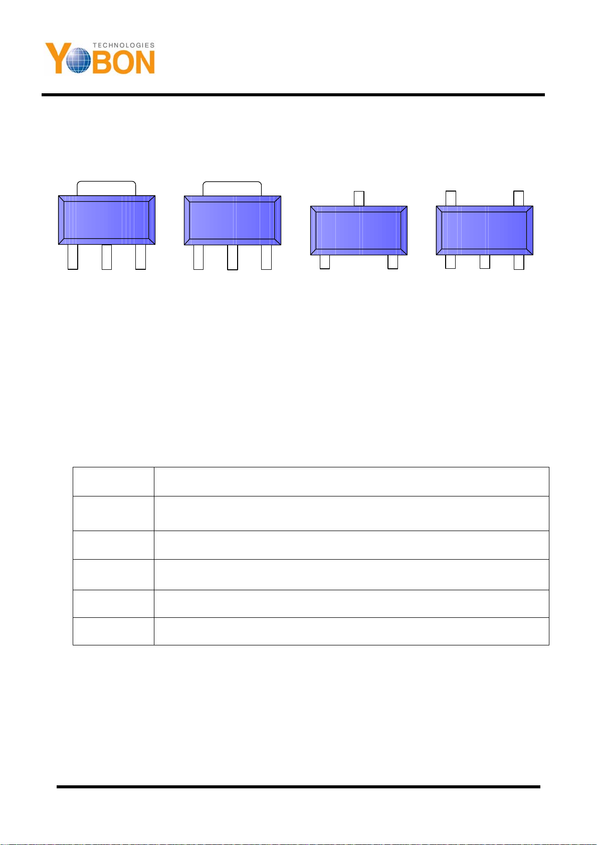
YB1253 regulators are available in SOT-23
/ SOT-25 / SOT-89 packages.
Typical Application Circuitry
YB1253
Features
• High Accuracy Output Voltage : + 2%
• Wide Output Voltage Range : 1.2~3.6V
• Ultra-Low-Noise Low-Drop-Out
• Typical Output Current : 300 mA
• Low Quiescent Current: ~10μA
• 300mV Dropout at 300mA 3.6V Output
• Stable with 1.0μF Ceramic Capacitor
• Only Need Input and Output Capacitors
• Thermal Protection Shutdown
• Auto discharge function
• Green Package (RoHS) Available
Applications
• PDA, Notebook, PC Computers
• DSC, Cellular phones
• PCMCIA Cards, PC Cameras
• USB Based Portable Devices
• GSM/GPRS/3G RF Transceiver
• Wireless LANs
• Bluetooth Portable Radios
• Battery-Powered Devices
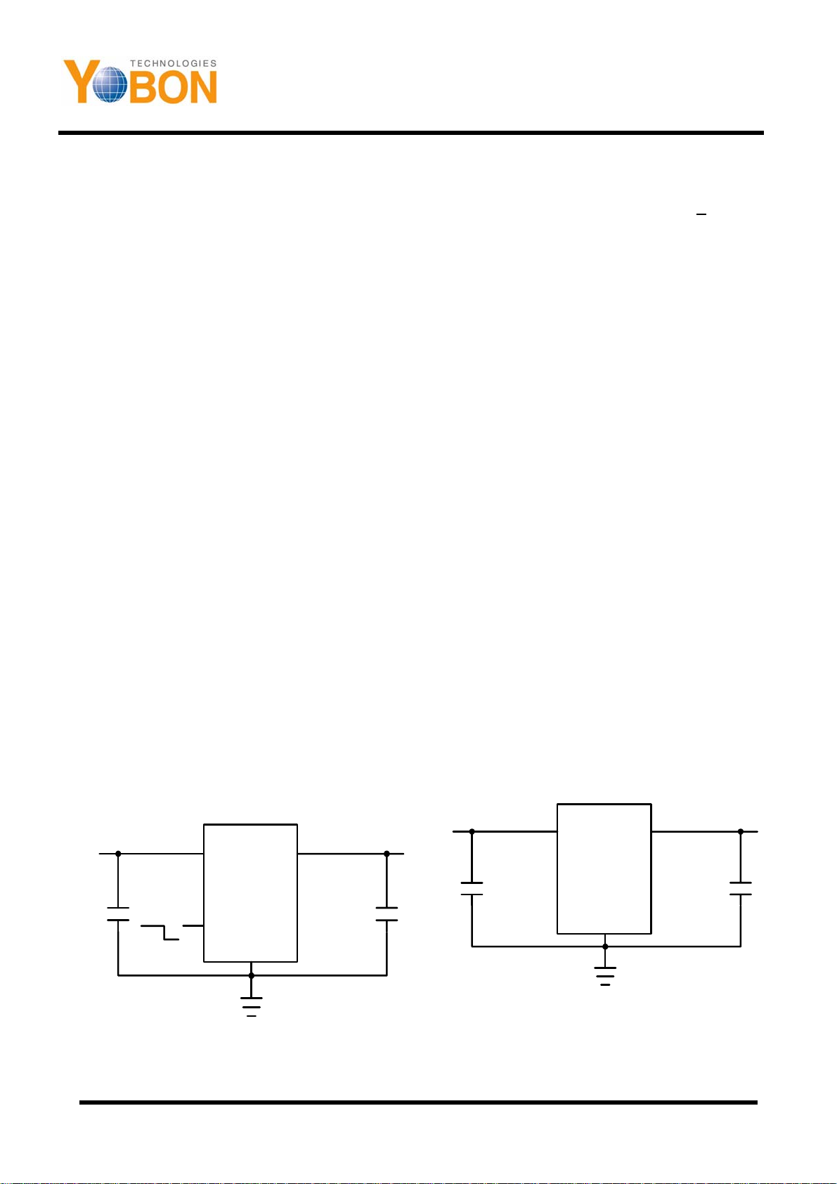
Input
Cin=1uF
ON
OFF
VIN VOUT
YB1253
EN
GND
Output
Cout=1uF
Input
Cin=1uF
Figure 1-2 : SOT-23 application circuit
VIN VOUT
YB1253
GND
Output
Cout=1uF
Figure 1-1 : SOT-25 application circuit
YB1253 Rev. 1.5 www.yobon.com.tw 1
Page 2
Pin Configuration
SOT-89
123
GND VIN
VOUT
YB1253
300mA, Low Power, High PSRR LDO Regulator
NC
4
3
EN
SOT-89R
123
VOUT GND
Figure 2 : pin configuration
VIN
VIN
3
VOUT
5
SOT-23
12
VOUTGND
1
VIN
SOT-25
2
GND
Pin Description
Table 1
Pin Name Pin Function
VIN
Unregulated Input Supply. Bypass with a capacitor to GND
GND Ground pin
EN Pull high to enable the regulator
NC No connection is required
VOUT Regulated Output Voltage
YB1253 Rev. 1.5 www.yobon.com.tw 2
Page 3
300mA, Low Power, High PSRR LDO Regulator
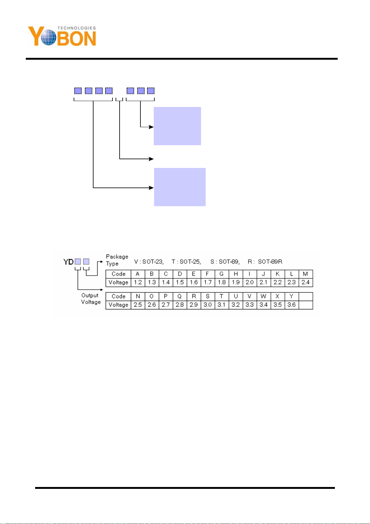
Ordering Information
YB1253
X
Output Voltage
120 : 1.2V
130 : 1.3V
:
360 : 3.6V
X : fix ed
Package Type
ST23 : SOT-23
ST25 : SOT-25
ST89 : SOT-89
ST8R : SOT-89R
YB1253
*Order example :
YB1253 ST 89X250 for YB1253 of
2.5V output and SOT-89 package
*Shipping Quantity :
SOT-23 : 3000 units tape & reel
SOT-25 : 3000 units tape & reel
SOT-89 : 1000 units tape & reel
SOT-89R : 1000 units tape & reel
*Only green package
Marking Information
Absolute Maximum Ratings (Note 1)
Supply Voltage ................................-0.3V to 6.0V
Output Voltage .......................-0.3V to (V
Output Short-Circuit Duration.................... Infinite
Junction Temperature Range................... +150℃
Storage Temperature Range ...... -65℃ to +150℃
Lead Temperature.................................... +250℃
ESD Susceptibility (HBM)…………… ………2KV
ESD Susceptibility (MM) ............................. 200V
Note:
1. Exceeding these ratings may damage the device.
2. The device is not guaranteed to function outside of its operating conditions.
3. θ
is measured in free air at TA = 25℃ on a low effective thermal conductivity board.
JA
+0.3V)
IN
Recommended Operating Conditions
Input Supply Voltage.........................2V to 5.5V
Operating Temperature..............-40℃ to +85℃
Thermal Information (Note 3)
Thermal Resistance (SOT-23/25, θJA).280℃/W
Thermal Resistance (SOT-89, θJA)…...180℃/W
Internal Power Dis si pat io n (SOT-23/25, PD)……0.4W
Internal Power Dissipation (SOT-89, PD)0.55W
(Note 2)
YB1253 Rev. 1.5 www.yobon.com.tw 3
Page 4

YB1253
300mA, Low Power, High PSRR LDO Regulator
Electrical Characteristics
Table 2
TA = 25℃, V
Function Parameter Conditions Min Typ Max Units
Input Voltage Range 2.0 5.5 V
Output Voltage, VOUT Predefined 1.2 3.6 V
Output Voltage Accuracy
Output Current Limit Short-circuit output 500 mA
IN
= ( V
+ 1 V ), C
OUT
= C
IN
I
= 10mA, VOUT >= 1.3V -2.0 +2.0 %
OUT
I
= 10mA, VOUT = 1.2V 0 +4.0 %
OUT
Vout = 3.6V, Iout = 300 mA 300
Vout = 3.3V, Iout = 300 mA 350
= 1.0μF, V
OU T
EN
= V
unless otherwise
IN,
Dropout Voltage (Note 1)
Ground Current Iground = Iin - Iout 10 μA
Line Regulation Vin = (Vout+1V) to 5.5V, Iout =10mA 0.10 0.20 %/V
Load Regulation Iout = 1mA to 300 mA 0.005 0.01 %/mA
Shutdown Supply Current EN = Vin=0V 1 μA
Ripple Rejection (PSRR)
Start Up Delay (Note 3) Rload=100ohm 200 μS
Shutdown Delay
EN Logic Low Level Vin = 2.0V to 5.5V 0.4 V
EN Logic High Level Vin = 2.0V to 5.5V 1.2 Vin V
EN Input Bias Current Vin = EN = 3V 1.5 μA
Thermal Shutdown Shutdown Temperature 160 °C
Thermal Hysteresis 20 °C
Note 1: The dropout voltage varies depending on output voltage selection. Dropout is defined as VIN–V
below nominal V
where Vin=Vout + 1V for nominal V
OUT
Vout = 2.8V, Iout = 300 mA 430
Vout = 1.8V, Iout = 300 mA 600
Vout = 1.2V, Iout = 300 mA 900
(Note 2)
Rload=10K ohm, VOUT=1.5V 1 mS
R
load=10K ohm, VOUT=1.2V 1 mS
.
OUT
50 dB
when V
OUT
OUT
mV
is 100mV
Note 2: PSRR is tested at Vin=3.8+1Vppac, Vout=2.8V, I_load=1mA.
Note 3: Time needed for V
to reach 90% of final value.
OUT
YB1253 Rev. 1.5 www.yobon.com.tw 4
Page 5

300mA, Low Power, High PSRR LDO Regulator
Typical Characteristics
At TA=25℃, VIN=(V
Output Curent VS Dropout voltage
1000
900
Iout= 300mA
800
700
600
500
400
300
Dropout Vo ltage (mV)
200
100
0
0 50 100 150 200 250 300 350
+1V), CIN=C
OUT
1.3V
1.8V
Output current (mA)
3.3V
=1.0μF, VEN=VIN, unless otherwise noted.
OUT
Input voltage VS Quiescent current
45
40
35
30
25
20
15
Quiescent current (uA)
10
5
0
Iout= 0
2 2.5 3 3.5 4 4.5 5 5.5
input voltage (V)
YB1253
3.3V
1.8V
Output voltage VS Temperature
3.5
3
Iout= 300mA
2.5
2
1.5
Outpu t Voltag e (V)
1
0.5
0
50 60 70 80 90 100 110 120 130
3.3V
1.8V
Temperature (degree)
Startup delay time
Rout = 10Ω
Vout = 3.3V
EN
Output voltage VS Output current
3.5
3
2.5
2
1.5
Ouput voltage (V)
1
0.5
0
0 50 100 150 200 250 300
3.3V
1.8V
Output current (mA)
Shutdown delay time
Rout = 10Ω
EN
Vout = 3.3V
Vout
Vout
YB1253 Rev. 1.5 www.yobon.com.tw 5
Page 6

Vout
VIN
Input transient response
4V
YB1253
300mA, Low Power, High PSRR LDO Regulator
Load transient response
Iout=100mA
Vout =3.3V
6V
Iout
250mA
10mA 10mA
Vout
VIN=4.3V
Vout =3.3V
Power supply rejection ratio
Vin=3.8VDC + 1V
Vout=2.8V
Iout=1mA
, Cout=1.0μF
P-P
Power supply rejection ratio
Vin=3.8V
Vout=2.8V
Iout=10mA
+ 1V
DC
, Cout=1.0μF
P-P
YB1253 Rev. 1.5 www.yobon.com.tw 6
Page 7

300mA, Low Power, High PSRR LDO Regulator
Functional Block Diagram
EN
Vref
Thermal
shutdown
YB1253
VIN
VOUT
GND
Figure 3 : Function diagram
Functional Description
The YB1253 is an ultra-low-noise, low-quiescent
current, low-dropout linear regulator. It is supplied in
a SOT-23 / SOT-25 / SOT-89 package for different
applications. YB1253 can supply load current up to
300mA (typical operation, not maximum) with good
line and load regulation. Output voltages are preset
and ranging from 1.2V to 3.6V.
As shown in the Functional Block Diagram, the
YB1253 consists of a reference and noise bypass
circuit, error amplifier, output drive transistor, internal
feedback voltage divider, thermal sensor, and short
circuit current limiter.
The internal reference is connected to the error
amplifier’s inverting input. The error amplifier
compares this reference with the feedback voltage
Short Circuit
Protection
and amplifies the difference. If the feedback voltage
is lower than the reference voltage, the gate of the
pass-transistor is pulled low. This allows more
current to pass to the output and increases the
output voltage. If the feedback voltage is too high,
the gate of the pass transistor is pulled high,
allowing less current to pass to the output.
Stability
The YB1253 is a high performance LDO
emphasizing stability with low output capacitance. It
is able to maintain stability with an output capacitor
as low as 1.0µF. The output capacitor can also be
increased to optimize performance. The YB1253 will
remain stable and in regulation with no load, unlike
many other voltage regulators.
YB1253 Rev. 1.5 www.yobon.com.tw 7
Page 8

300mA, Low Power, High PSRR LDO Regulator
Internal P-Channel Pass Transistor
The YB1253 features a low impedance P-channel
MOSFET pass transistor. This provides several
advantages over similar designs using a PNP pass
transistor, including low operating power and longer
battery life. The YB1253 consumes only 10µA of
quiescent current under most conditions.
Output Short-Circuit Current Limit
The YB1253 includes a current limiter, which
monitors and controls the pass transistor’s gate
voltage, limiting the output current to about 500mA,
for example, in a short-circuit output situation.
Shutdown
The YB1253 also features a low-power active
shutdown mode. It has a switch that turns off the
device when disabled. This allows the output
capacitor and load to discharge and de-energize the
load. In the shutdown mode, the internal functional
blocks, such as voltage reference and the error
amplifier are turned off completely, and the
quiescent current is less than 1µA.
YB1253
Application Information
Enable/Shutdown
The YB1253 comes with an active-high enable pin
that allows the regulator to be enabled. Forcing the
enable pin low disables the regulator and puts it into
the shutdown mode. This pin cannot be left floating
as it may cause an undetermined state.
Input/Output Capacitor
It is recommended to use a 1.0µF capacitor in the
YB1253 input and a 1.0µF capacitor in the output.
For high regulation performance, larger input
capacitor values and lower ESRs provide better
noise rejection and line-transient response. The
output noise, load-transient response, stability, and
power-supply rejection can be improved by using
large output capacitors. Low ESR ceramic
capacitors provide optimal performance and save
space.
Thermal Protection Shutdown
The thermal protection shutdown function protects
the device from operating in over temperature
condition. When the junction temperature exceeds
+160°C, the thermal sensor signals the shutdown
logic, turning off the pass transistor and allowing the
IC to cool down. The thermal sensor turns the pass
transistor on again after the IC’s junction
temperature drops to +140°C.
YB1253 Rev. 1.5 www.yobon.com.tw 8
Page 9

300mA, Low Power, High PSRR LDO Regulator
SOT-25 Package Information
A1 A2
bx5
A
L1
e1
YB1253
E1
D
e
E
L2
GAUGE PLANE
t
C
L
milimeters Inches
Symbol
MIN.
MAX.
MIN.
MAX.
A
0.95 1.45 .037 .057
A1
0.05 0.15 .002 .006
A2
0.90 1.30 .035 .051
b
0.30 0.50 .0118 .019
C
0.08 0.20 .0031 .0078
D
2.84 3.00 .1118 .118
E
1.50 1.70 .059 .0669
E1
2.60 3.00 .102 .118
e
e1
L
L1
L2
t
0.95 BSC.
1.90 BSC.
0.35 0.55 .0137 .0216
0.10 BSC.
0.60 REF.
0° 8° 0° 8°
.0374 BSC.
.0748 BSC.
.0039 BSC.
.0236 REF.
YB1253 Rev. 1.5 www.yobon.com.tw 9
Page 10

300mA, Low Power, High PSRR LDO Regulator
SOT-23 Package Information
A1 A2
b?3
A
e1
YB1253
E1
D
e
E
L2
GAUGE PLANE
L1
C
milimeters Inches
MIN.
Symbol
A
0.95 1.45 .037 .057
A1
0.05 0.15 .002 .006
A2
0.90 1.30 .035 .051
b
0.30 0.50 .0118 .019
C
0.08 0.20 .0031 .0078
D
2.84 3.00 .1118 .118
E
1.50 1.70 .059 .0669
E1
2.60 3.00 .102 .118
e
e1
L
L1
L2
t
0.95 BSC.
1.90 BSC.
0.35 0.55 .0137 .0216
0.10 BSC.
0.60 REF.
0° 8° 0° 8°
L
MAX.
MIN.
t
MAX.
.0374 BSC.
.0748 BSC.
.0039 BSC.
.0236 REF.
YB1253 Rev. 1.5 www.yobon.com.tw 10
Page 11

300mA, Low Power, High PSRR LDO Regulator
SOT-89 Package Information
e1
YB1253
bx2 b1
e
E1
D
b2
E
L
A
Symbol
A
b
b1
b2
C
D
E
E1
e
e1
L
milimeters Inches
MIN.
1.40 1.60 .055 .063
0.36 0.48 .014 .019
0.44 0.56 .017 .022
1.50 1.83 .059 .072
0.35 0.44 .014 .017
4.40 4.60 .173 .181
2.29 2.60 .090 .102
3.94 4.25 .155 .167
1.50 BSC.
3.00 BSC.
0.89 1.20 .035 .047
MAX.
C
MIN.
.059 BSC.
.118 BSC.
MAX.
YB1253 Rev. 1.5 www.yobon.com.tw 11
Page 12

 Loading...