

Page 1

SA5224
FDDI fiber optic postamplifier
Product specification
Replaces datasheet NE/SA5224 of 1995 Apr 26
IC19 Data Handbook
1998 Oct 07
INTEGRATED CIRCUITS
Page 2
Philips Semiconductors Product specification
SA5224FDDI fiber optic postamplifier
2
1998 Oct 07 853-1594 20141
DESCRIPTION
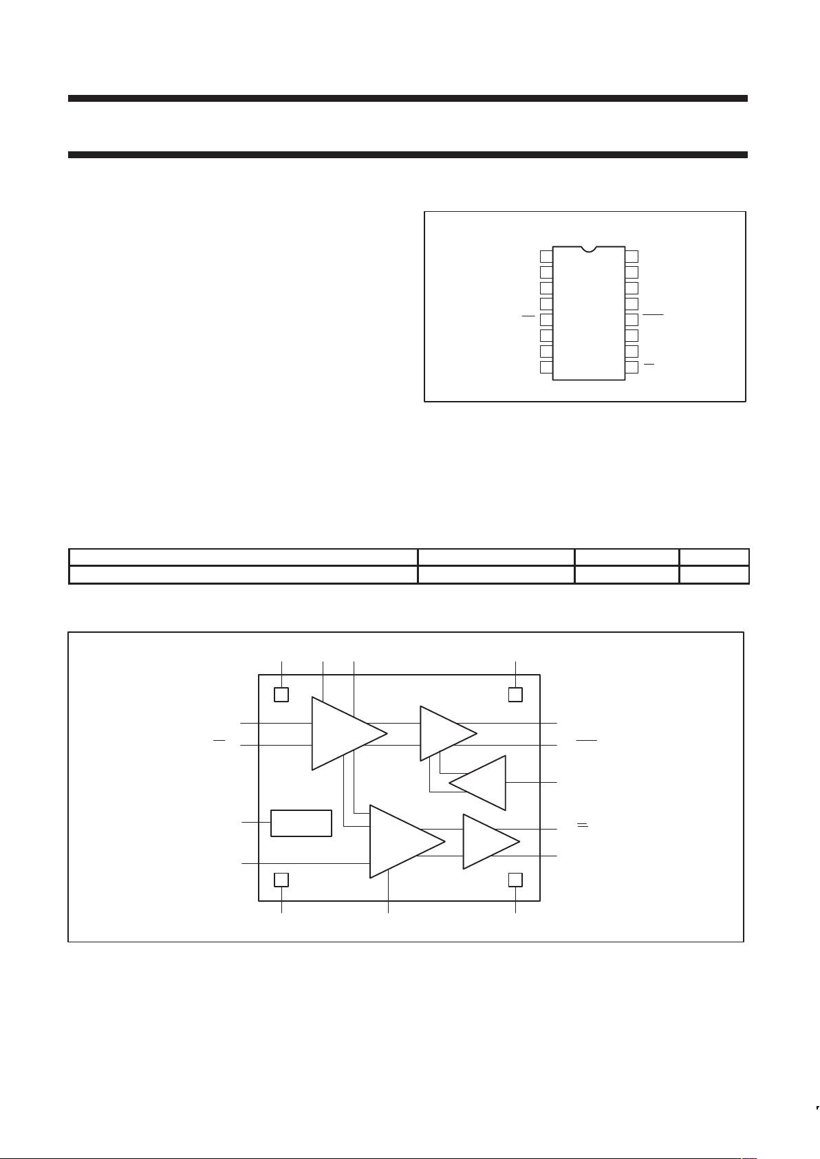
The SA5224 is a high-gain limiting amplifier that is designed to
process signals from fiber optic preamplifiers. Capable of operating
at 125Mb/s, the chip is FDDI compatible and has input signal
level-detection with a user-adjustable threshold. The DATA and
LEVEL-DETECT outputs are differential for optimum noise margin
and ease of use. Also available is the SA5225 which is an ECL 10K
version of the SA5224.
FEA TURES
•Wideband operation: 1.0kHz to 120MHz typical
•Applicable in 155Mb/s OC3/SONET receivers
•Operation with single +5V or –5.2V supply
•Differential 100k ECL outputs
•Programmable input signal level-detection
•Fully differential for excellent PSRR to 1GHz
PIN DESCRIPTION
D Package
CAZN
CAZP
GND
A
D
IN
D
OUT
D
OUT
V
REF
V
SET
1
2
3
4
5
6
7
8
9
10
11
12
13
14
16
15
D
IN
CF
JAM
V
CCA
V
CCE
GND
E
ST
ST
SD00374
Figure 1. Pin Configuration
APPLICATIONS
•FDDI
•Data communication in noisy industrial environments
•LANs
ORDERING INFORMATION
DESCRIPTION TEMPERATURE RANGE ORDER CODE DWG #
16-Pin Plastic Small Outline (SO) package
–40 to +85°C
SA5224D SOT109-1
BLOCK DIAGRAM
(6) (2) (1) (16)
(13)
(12)
(8)
(9)
(10)
(11)(7)(3)
(16)
(15)
(5)
(4)
LIMITING
AMPLIFIER
ECL
BUFFER
JAM
BUFFER
SD
BUFFER
LEVEL
DETECTOR
REFERENCE
D
IN
D
IN
V
REF
V
SET
GND
A
C
F
GND
E
D
OUT
D
OUT
JAM
ST
V
CCE
C
AZN
C
AZP
V
CCA
ST
SD00375
Figure 2. Block Diagram
Page 3

Philips Semiconductors Product specification
SA5224FDDI fiber optic postamplifier
1998 Oct 07
3
PIN DESCRIPTIONS
PIN NO. NAME FUNCTION
1 C
AZN
Auto-zero capacitor pin. Connecting a capacitor between this pin and C
AZP
will cancel the offset voltage of the
limiting amplifier.
2 C
AZP
Auto-zero capacitor pin. Connecting a capacitor between this pin and C
AZN
will cancel the offset voltage of the
limiting amplifier.
3 GNDAAnalog GND pin. Connect to ground for +5V upshifted ECL operation. Connect to –5.2V for standard ECL
operation. Must be at same potential as GNDE (Pin 11).
4 D
IN
Differential input. DC bias level is set internally at approximately 2.9V. Complimentary to DIN (Pin 5).
5 D
IN
Differential input. DC bias level is set internally at approximately 2.9V. Complimentary to DIN (Pin 4).
6 V
CCA
Analog power supply pin. Connect to a +5V supply for upshifted ECL operation. Connect to ground for standard
ECL operation. Must be at same potential as V
CCE
(Pin 14).
7 C
F
Filter capacitor for level detector. Capacitor should be connected between this pin and V
CCA
.
8 JAM This ECL-compatible input controls the output buffers D
OUT
and D
OUT
(Pins 12 and 13). When an ECL LOW signal
is applied, the outputs will follow the input signal. When an ECL HIGH signal is applied, the D
OUT
and D
OUT
pins
will latch into LOW and HIGH states, respectively. When left unconnected, this pin is actively pulled-low (JAM OFF).
9
ST
Input signal level-detect STATUS. This ECL output is high when the input signal is below the user programmable
threshold level.
10 ST ECL compliment of ST (Pin 9).
11 GNDEDigital GND pin. Connect to ground for +5V upshifted ECL operation. Connect to a negative supply for normal ECL
operation. Must be at the same potential as GNDA (Pin 3).
12
D
OUT
ECL-compatible output. Nominal level is V
CCE
–1.3V. When JAM is HIGH, this pin will be forced into an ECL HIGH
condition. Complimentary to D
OUT
(Pin 13).
13 D
OUT
ECL-compatible output. Nominal level is V
CCE
–1.3V. When JAM is HIGH, this pin will be forced into an ECL LOW
condition. Complimentary to D
OUT
(Pin 12).
14 V
CCE
Digital power supply pin. Connect to a +5V supply for upshifted ECL operation. Connect to ground during normal
ECL operation. Must be at the same potential as V
CCA
(Pin 6).
15 V
REF
Reference voltage for threshold level voltage divider. Nominal value is approximately 2.64V.
16 V
SET
Input threshold level setting circuit. This input can come from a voltage divider between V
REF
and GNDA.
ABSOLUTE MAXIMUM RATINGS
SYMBOL PARAMETER RATING UNITS
V
CC
Power supply (VCC - GND) 6 V
T
A
Operating ambient –45 to +85
°C
T
J
Operating junction –55 to +150
°C
T
STG
Storage –65 to +150
°C
P
D
Power dissipation, TA = 25°C (still air)
1
16-pin Plastic SO
1100 mW
NOTE:
1. Maximum dissipation is determined by the ambient temperature and the thermal resistance,
θ
JA
: 16-pin SO: θJA = 110°C/W
RECOMMENDED OPERATING CONDITIONS
SYMBOL PARAMETER RATING UNITS
V
CC
Supply voltage 4.5 to 5.5 V
T
A
Ambient temperature ranges –40 to +85
°C
T
J
Junction temperature ranges –40 to +110
°C
Page 4
Philips Semiconductors Product specification
SA5224FDDI fiber optic postamplifier
1998 Oct 07
4
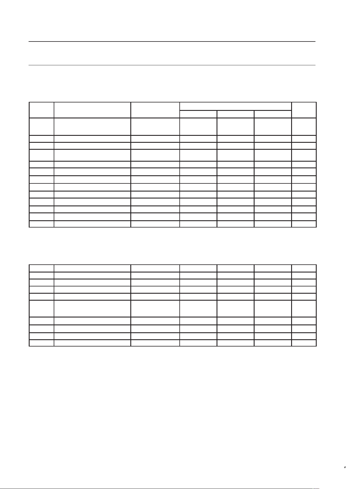
DC ELECTRICAL CHARACTERISTICS
Min and Max limits apply over operating temperature at VCC = 5V ±10%, unless otherwise specified. Typical data apply at TA = 25°C and VCC =
+5V.
SA5224
SYMBOL
PARAMETER
TEST CONDITIONS
Min Typ Max
UNIT
V
IN
Input signal voltage
single-ended
differential
.002
.004
1.5
3.0
V
P-P
V
OS
Input offset voltage
2
50 µV
V
N
Input RMS noise
2
60 µV
V
TH
Input level-detect programmability
single-ended
VIN = 200kHz square
wave
2 12 mV
P-P
V
HYS
Level-detect hysteresis 4 5 6 dB
I
CC
V
CCA
+ V
CCE
supply current No ECL loading 27 35
mA
I
INL
JAM input current Pin 8 = 0V –10 10
µA
V
OHMAX
Maximum logic high
1
–0.880
V
DC
V
OHMIN
Minimum logic high
1
–1.055 V
DC
V
OLMAX
Maximum logic low
1
–1.620
V
DC
V
OLMIN
Minimum logic low
1
–1.870 V
DC
V
IH
Minimum input for JAM = high
1
–1.165
V
DC
V
IL
Maximum input for JAM = low
1
–1.490 V
DC
NOTES:
1. These ECL specifications are referenced to the V
CCE
rail and apply for TA = 0°C to 85°C.
2. Guaranteed by design.
AC ELECTRICAL CHARACTERISTICS
Typical data apply at TA = 25°C and VCC = +5V . Min and Max limits apply for 4.5 ≤ VCC ≤ 5.5V.
SYMBOL
PARAMETER TEST CONDITIONS Min Typ Max UNIT
BW
1
Lower –3dB bandwidth CAZ = 0.1µF 0.5 1.0 1.5 kHz
BW
2
Upper –3dB bandwidth 90 120 150 MHz
R
IN
Input resistance Pin 4 or 5 2.9 4.5 7.6 kΩ
C
IN
Input capacitance Pin 4 or 5 2.5 pF
tr, t
f
ECL output
3
risetime,
falltime
RL = 50Ω
To V
CCE
- 2V
20-80%
1.2 2.2 ns
t
PWD
Pulsewidth distortion 0.3
ns
P-P
R
AZ
Auto zero output resistance Pin 1 or 2 155 250 423
kΩ
R
F
Level-detect filter resistance Pin 7 14 24 41 kΩ
t
LD
Level-detect time constant CF = 0 0.5 1.0 2.0 µs
NOTES:
1. Both outputs should be terminated identically to minimize differential feedback to the device inputs on a PC board or substrate.
Page 5
Philips Semiconductors Product specification
SA5224FDDI fiber optic postamplifier
1998 Oct 07
5
NE5212 NE5224
CLOCK
RECOVERY
&
RETIMING
SD00376
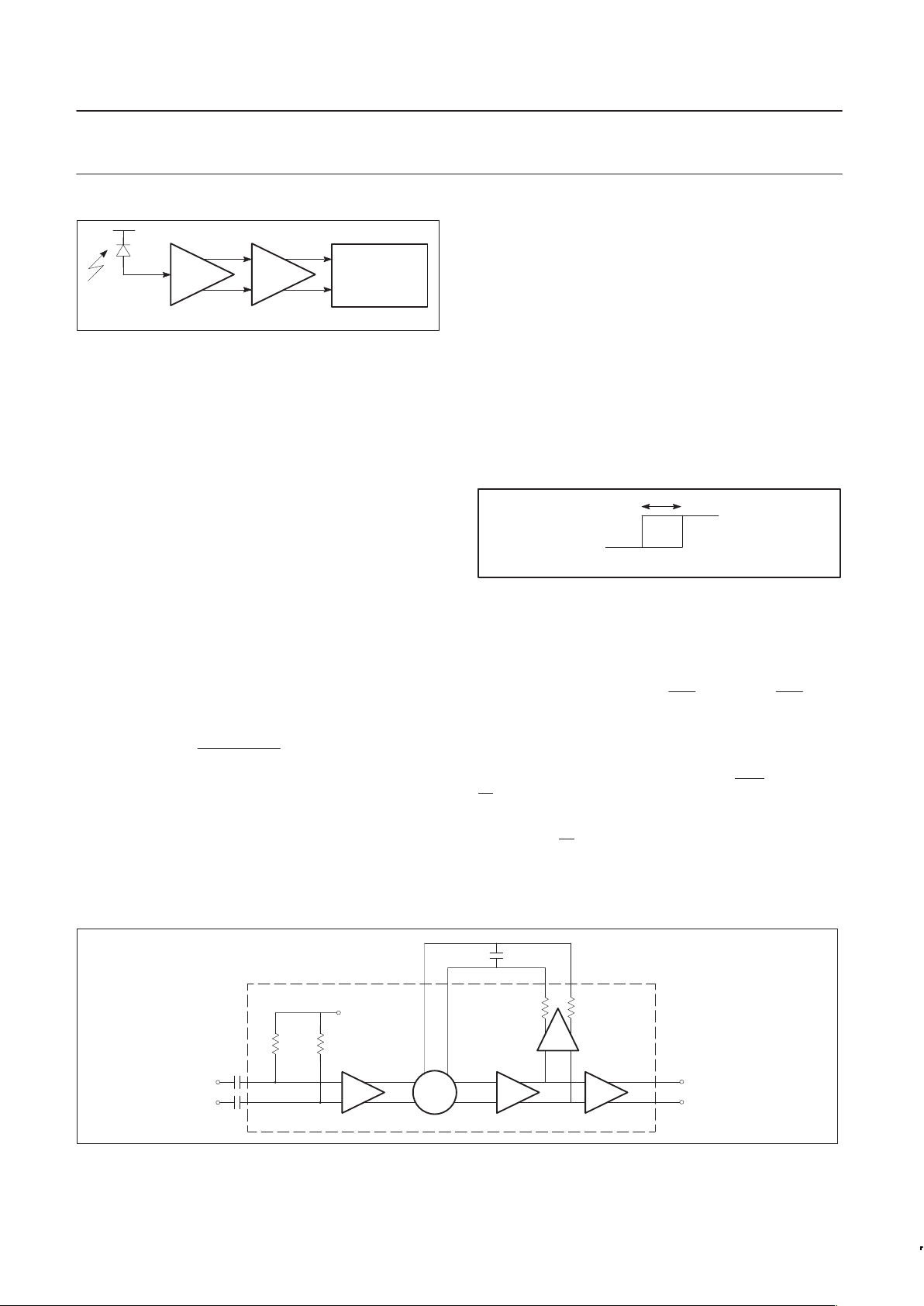
Figure 3. Typical Fiber Optic Receiving System
INPUT BIASING
The DATA INPUT pins (4 and 5) are DC biased at approximately
2.9V by an internal reference generator. The SA5224 can be DC
coupled, but the driving source must operate within the allowable
1.4V to 4.4V input signal range (for VCC = 5V). If AC coupling is
used to remove any DC compatibility requirement, the coupling
capacitors C1 and C2 must be large enough to pass the lowest input
frequency of interest. For example, .001µF coupling capacitors
react with the internal 4.5k input bias resistors to yield a lower –3dB
frequency of 35kHz. This then sets a limit on the maximum number
of consecutive “1”s or “0”s that can be sensed accurately at the
system data rate. Capacitor tolerance and resistor variation (2.9k to
7.6k) must be included for an accurate calculation.
AUTO-ZERO CIRCUIT
Figure 5 also shows the essential details of the auto-zero circuit. A
feedback amplifier (A4) is used to cancel the offset voltage of the
forward signal path, so the input to the internal ECL comparator (A6)
is at its toggle point in the absence of any input signal. The time
constant of the cancelling circuitry is set by an external capacitor
(C
AZ
) connected between Pins 1 and 2. The formula for the lower
–3dB frequency is:
f
3dB
150
2 R
AZ
C
AZ
where RAZ is the internal driving impedance which can vary from
155k to 423k over temperature and device fabrication limits. The
input coupling time constant must also be considered in determining
the lower frequency response of the SA5224.
INPUT SIGNAL LEVEL-DETECTION
The SA5224 allows for user programmable input signal
level-detection and can automatically disable the switching of its
ECL data outputs if the input is below a set threshold. This prevents
the outputs from reacting to noise in the absence of a valid input
signal, and insures that data will only be transmitted when the input
signal-to-noise ratio is sufficient for low bit-error-rate system
operation. Complimentary ECL flags (ST and STB) indicate whether
the input signal is above or below the desired threshold level.
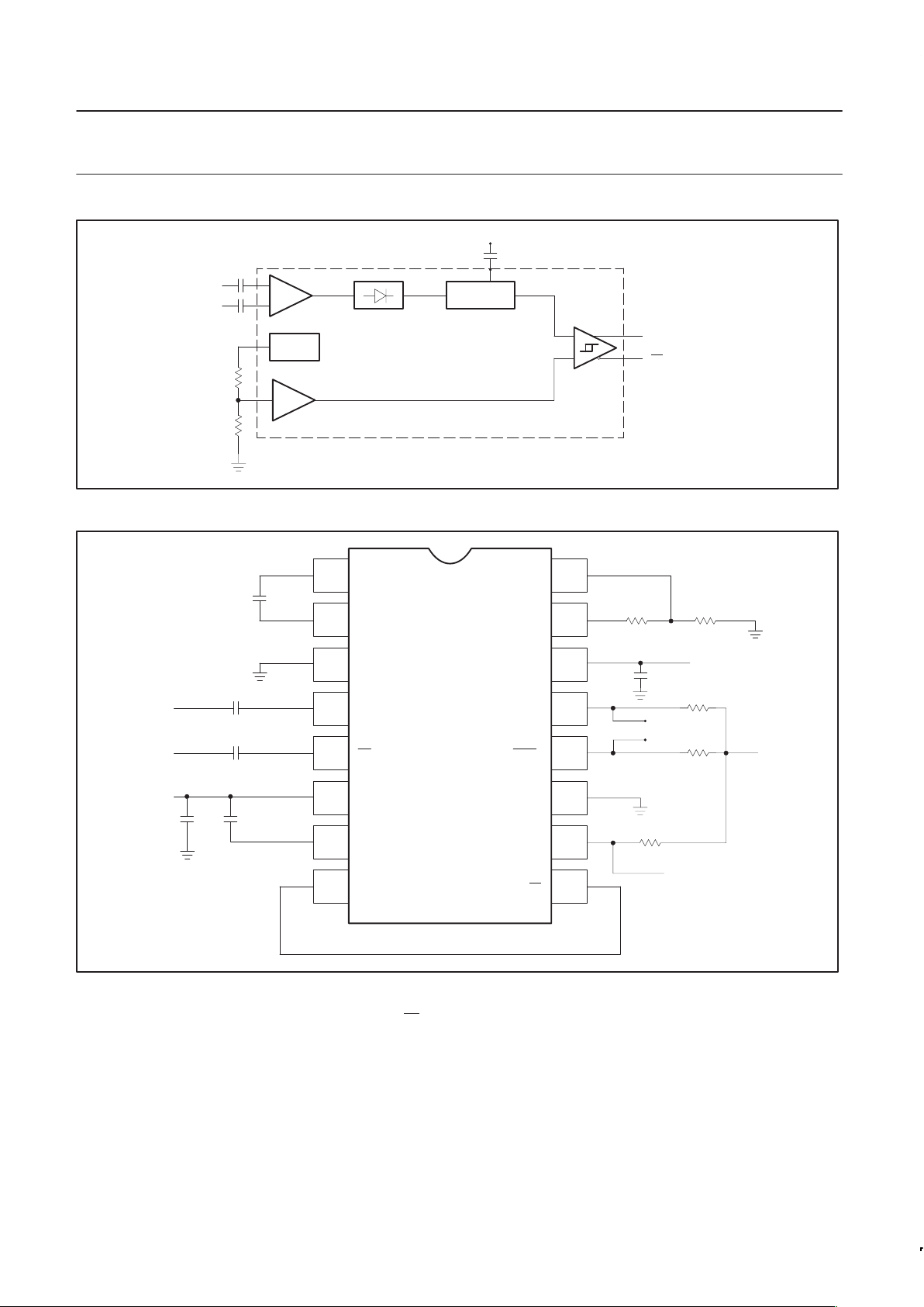
Figure 6 shows a simplified block diagram of the SA5224
level-detect system. The input signal is amplified and rectified
before being compared to a programmable reference. A filter is
included to prevent noise spikes from triggering the level-detector.
This filter has a nominal 1µs time constant, and additional filtering
can be achieved by using an external capacitor (CF) from Pin 7 to
V
CCA
(the internal driving impedance is nominally 24k). The
resultant signal is then compared to a programmable level, V
SET
,
which is set by an internal voltage reference (2.64V) and an external
resistor divider (R1 and R2). The value of R1 + R2 should be
maintained at approximately 5k.
HYST
(OFF) (ON)
V
TL
V
TH
SD00377
Figure 4.
The circuit is designed to operate accurately over a differential
2-12mV
P-P
square-wave input level detect range. This level,
V
SET
/100, is the average of VTH and VTL.
Nominal hysteresis of 5dB is provided by the complimentary ECL
output comparator yielding
V
TL
V
SET
139
and
V
TH
V
SET
78
. For
example, with V
SET
= 1.2V , a 15.4mV
P-P
square-wave differential
input will drive the ST pin high, and an input level below 8.6mV
P-P
will drive the ST pin low.
Since a “JAM” function is provided (Pin 8) and can force the data
outputs to a predetermined state (D
OUT
= LOW, D
OUT
= HIGH), the
ST
and JAM pins can be connected together to automatically
disable signal transmission when the chip senses that the input
signal is below the desired threshold. JAM (Pin 8) low enables the
Data Outputs. ST
will be in a high ECL state for input signals below
threshold.
DATA IN
C1
C2
A1 +
–
A3 A6 DATA OUT
A4
D
IN
D
INB
R
IN
C
AZ
R
AZ
250kΩ
R
AZ
250kΩ
D
OUT
D
OUTB
4.5kΩ
R
IN
4.5kΩ
V
BIAS
ECL 100k
SD00378
Figure 5. SA5224 Forward Gain Path Including Auto-Zero
Page 6
Philips Semiconductors Product specification
SA5224FDDI fiber optic postamplifier
1998 Oct 07
6
50X
.25X
R
1
C
F
V
CCA
FILTER
R
2
V
REF
DATA IN
2.64V
ST
LEVELDETECT
FLAGS
+
–
ST
LOW-PASS
ECL 100k
SD00379
Figure 6. SA5224 Input Signal Level-Detect System
R
1
C
AZ
R
2
C
IN1
DATA IN DATA OUT
3V
LEVEL-DETECT
STATUS
1
2
3
4
5
6
7
8
9
10
11
12
13
14
16
15
0.1µF
0.1µF
0.1µF 0.1µF
0.1µF
5V
C
IN2
0.1µF
R
3
R
4
R
5
50Ω
50Ω
50Ω
C
AZN
C
AZP
GND
A
D
IN
D
IN
V
CCA
C
F
JAM
V
SET
V
REF
V
CCE
D
OUT
D
OUT
GND
E
ST
ST
5V
SD00380
Figure 7. Application with VCC = 5.0V
NOTE: A 50Ω resistor is required from Pin 9 to 3V only if the ST
pin
is required to meet 100k ECL specifications.
Die Sales Disclaimer
Due to the limitations in testing high frequency and other parameters
at the die level, and the fact that die electrical characteristics may
shift after packaging, die electrical parameters are not specified and
die are not guaranteed to meet electrical characteristics (including
temperature range) as noted in this data sheet which is intended
only to specify electrical characteristics for a packaged device.
All die are 100% functional with various parametrics tested at the
wafer level, at room temperature only (25°C), and are guaranteed to
be 100% functional as a result of electrical testing to the point of
wafer sawing only. Although the most modern processes are
utilized for wafer sawing and die pick and place into waffle pack
carriers, it is impossible to guarantee 100% functionality through this
process. There is no post waffle pack testing performed on
individual die.
Page 7
Philips Semiconductors Product specification
SA5224FDDI fiber optic postamplifier
1998 Oct 07
7
Since Philips Semiconductors has no control of third party
procedures in the handling or packaging of die, Philips
Semiconductors assumes no liability for device functionality or
performance of the die or systems on any die sales.
Although Philips Semiconductors typically realizes a yield of 85%
after assembling die into their respective packages, with care
customers should achieve a similar yield. However, for the reasons
stated above, Philips Semiconductors cannot guarantee this or any
other yield on any die sales.
1
2
3
4
5
6
7
8910
11
12
13
14
15
16
CAZN
CAZP
GNDA
DIN
DIN
V
CCA
CF
JAM
ST
ST
GND
E
DOUT
V
CCE
V
REF
DOUT
V
SET
ECN No.: 01673
1991 Feb 8
SD00492
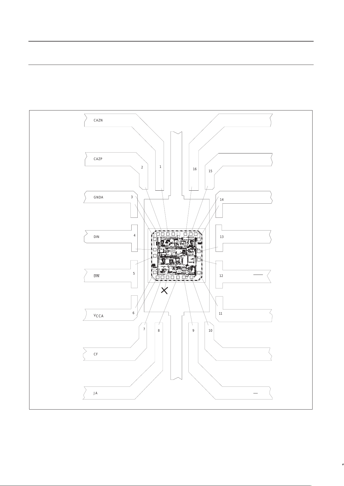
Figure 8. SA5224 Bonding Diagram
Page 8
Philips Semiconductors Product specification
SA5224FDDI fiber optic postamplifier
1998 Oct 07
8
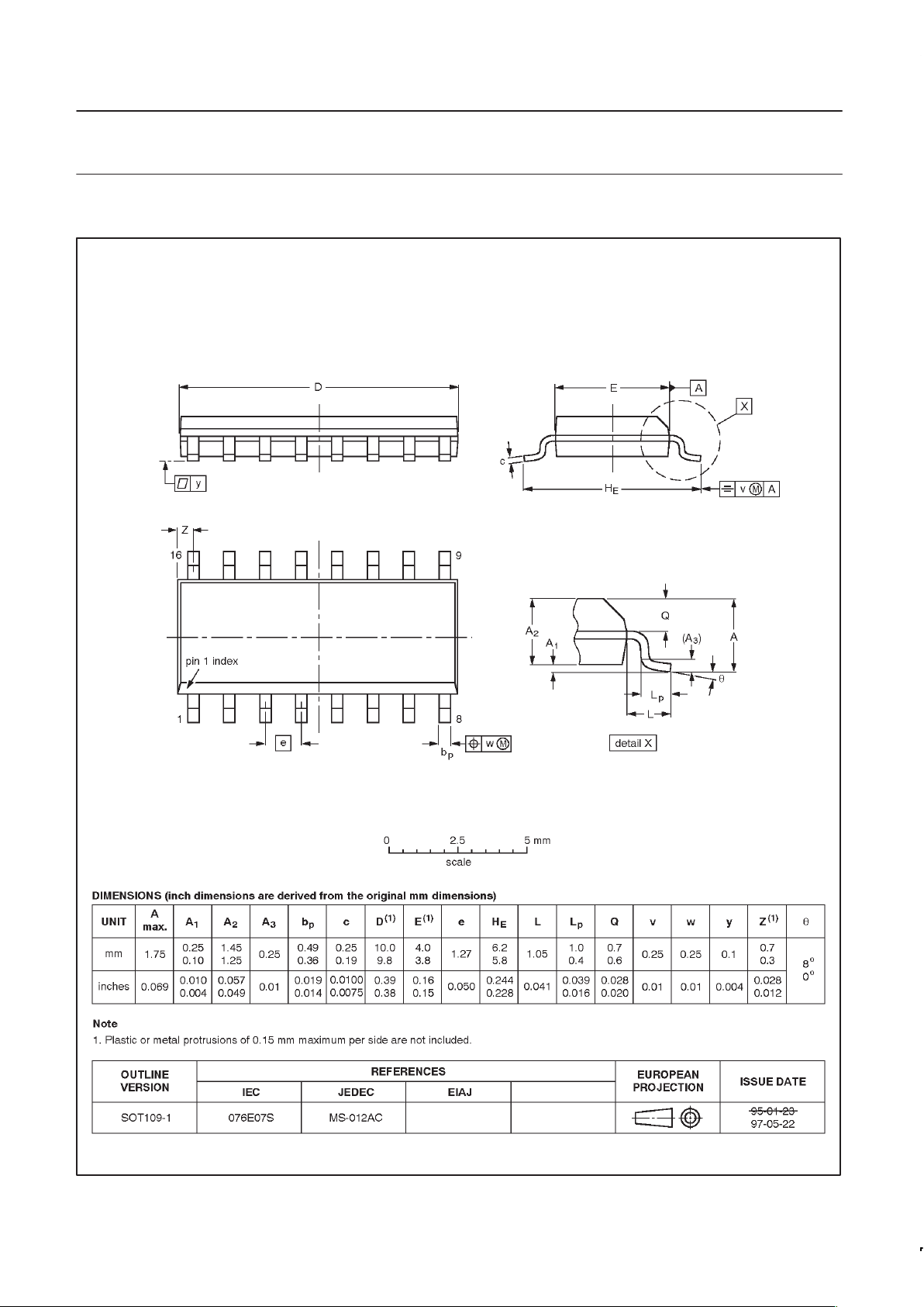
SO16: plastic small outline package; 16 leads; body width 3.9 mm SOT109-1
Page 9

Philips Semiconductors Product specification
SA5224FDDI fiber optic postamplifier
1998 Oct 07
9
NOTES
Page 10

Philips Semiconductors Product specification
SA5224FDDI fiber optic postamplifier
1998 Oct 07
10
Definitions
Short-form specification — The data in a short-form specification is extracted from a full data sheet with the same type number and title. For
detailed information see the relevant data sheet or data handbook.
Limiting values definition — Limiting values given are in accordance with the Absolute Maximum Rating System (IEC 134). Stress above one
or more of the limiting values may cause permanent damage to the device. These are stress ratings only and operation of the device at these or
at any other conditions above those given in the Characteristics sections of the specification is not implied. Exposure to limiting values for extended
periods may affect device reliability.
Application information — Applications that are described herein for any of these products are for illustrative purposes only. Philips
Semiconductors make no representation or warranty that such applications will be suitable for the specified use without further testing or
modification.
Disclaimers
Life support — These products are not designed for use in life support appliances, devices or systems where malfunction of these products can
reasonably be expected to result in personal injury . Philips Semiconductors customers using or selling these products for use in such applications
do so at their own risk and agree to fully indemnify Philips Semiconductors for any damages resulting from such application.
Right to make changes — Philips Semiconductors reserves the right to make changes, without notice, in the products, including circuits, standard
cells, and/or software, described or contained herein in order to improve design and/or performance. Philips Semiconductors assumes no
responsibility or liability for the use of any of these products, conveys no license or title under any patent, copyright, or mask work right to these
products, and makes no representations or warranties that these products are free from patent, copyright, or mask work right infringement, unless
otherwise specified.
Philips Semiconductors
811 East Arques Avenue
P.O. Box 3409
Sunnyvale, California 94088–3409
Telephone 800-234-7381
Copyright Philips Electronics North America Corporation 1998
All rights reserved. Printed in U.S.A.
Date of release: 10-98
Document order number: 9397 750 04628
Data sheet
status
Objective
specification
Preliminary
specification
Product
specification
Product
status
Development
Qualification
Production
Definition
[1]
This data sheet contains the design target or goal specifications for product development.
Specification may change in any manner without notice.
This data sheet contains preliminary data, and supplementary data will be published at a later date.
Philips Semiconductors reserves the right to make chages at any time without notice in order to
improve design and supply the best possible product.
This data sheet contains final specifications. Philips Semiconductors reserves the right to make
changes at any time without notice in order to improve design and supply the best possible product.
Data sheet status
[1] Please consult the most recently issued datasheet before initiating or completing a design.
 Loading...