

Page 1
DS082 (v1.2) November 5, 2001 www.xilinx.com 1
Preliminary Product Specification 1-800-255-7778
© 2001 Xilinx, Inc. All rights reserved. All Xilinx trademarks, registered trademarks, patents, and disclaimers are as listed at http://www.xilinx.com/legal.htm.
All other trademarks and registered trademarks are the property of their respective owners. All specifications are subject to change without notice.
Features
• In-system programmable 3.3V PR OMs for
configuration of Xilinx FPGAs
- Endurance of 2,000 program/erase cycles
- Program/erase over full military temperature range
• IEEE Std 1149.1 boundary-scan (JTAG) support
• Cascadable for storing longer or multiple bitstreams
• Dual configuration modes
- Serial Slow/Fast configuration (up to 33 MHz)
- Parallel (up to 264 Mbps at 33 MHz)
• Low-power advanced CMOS FLASH process
• 5V tolerant I/O pins accept 5V, 3.3V and 2.5V signals.
• 3.3V or 2.5V output capability
• Available in CC44 and VQ44 packages.
• Design suppor t using the Xilinx Alliance™ and
Foundation™ series software packages.
• JTAG command initiation of standard FPGA
configuration.
• Available to Standard Microcircuit Drawing
5962-01525.
- For more information contact Defense Supply
Center Columbus (DSCC) at
http://www.dscc.dla.mil
Radiation Hardenned XQR18V04
• Fabricated on Epitaxial Substrate
• Latch-Up Immune to >120 LET
• Guaranteed TID of 40 kRad(Si)
• Supports SEU Scrubbing
Description
Xilinx introduces the QPro™ XQ18V04 and XQR18V04
series of QML in-system programmable and radiation hardened configuration PROMs. Initial devices in this 3.3V family are a 4-megabit PROM that provide an easy-to-use,
cost-effective method for re-programming and storing large
Xilinx FPGA configuration bitstreams.
When the F PGA is in Master S erial mode, it generates a
configuration clock that drives the PROM. A short access
time after the r ising CCLK, data is available on the PROM
DATA (D0) pin that is connect ed to the FPGA D
IN
pin. The
FPGA generates the appropri ate number of clock pulses to
complete the configuration. When the FPGA is in Slave
Serial mode, the PROM and the FPGA are c locked by an
external clock.
When the FPGA is in Express or SelectMAP Mode, an
external oscillator will generate t he configuration c lock that
drives the PROM and the FPGA. After the rising CCLK
edge, data are available on the PROMs D ATA (D0-D7) pins.
The data will be clocked into the FPGA on the following rising edge of the CCLK. Neither Express nor SelectMAP utilize a Length Count, so a free-running oscillator may be
used. See Figure 6.
0
QPro XQ18V04 (XQR18V04) QML
In-System Programmable
Configuration PROMs
DS082 (v1.2) November 5, 2001
05
Preliminary Product Specification
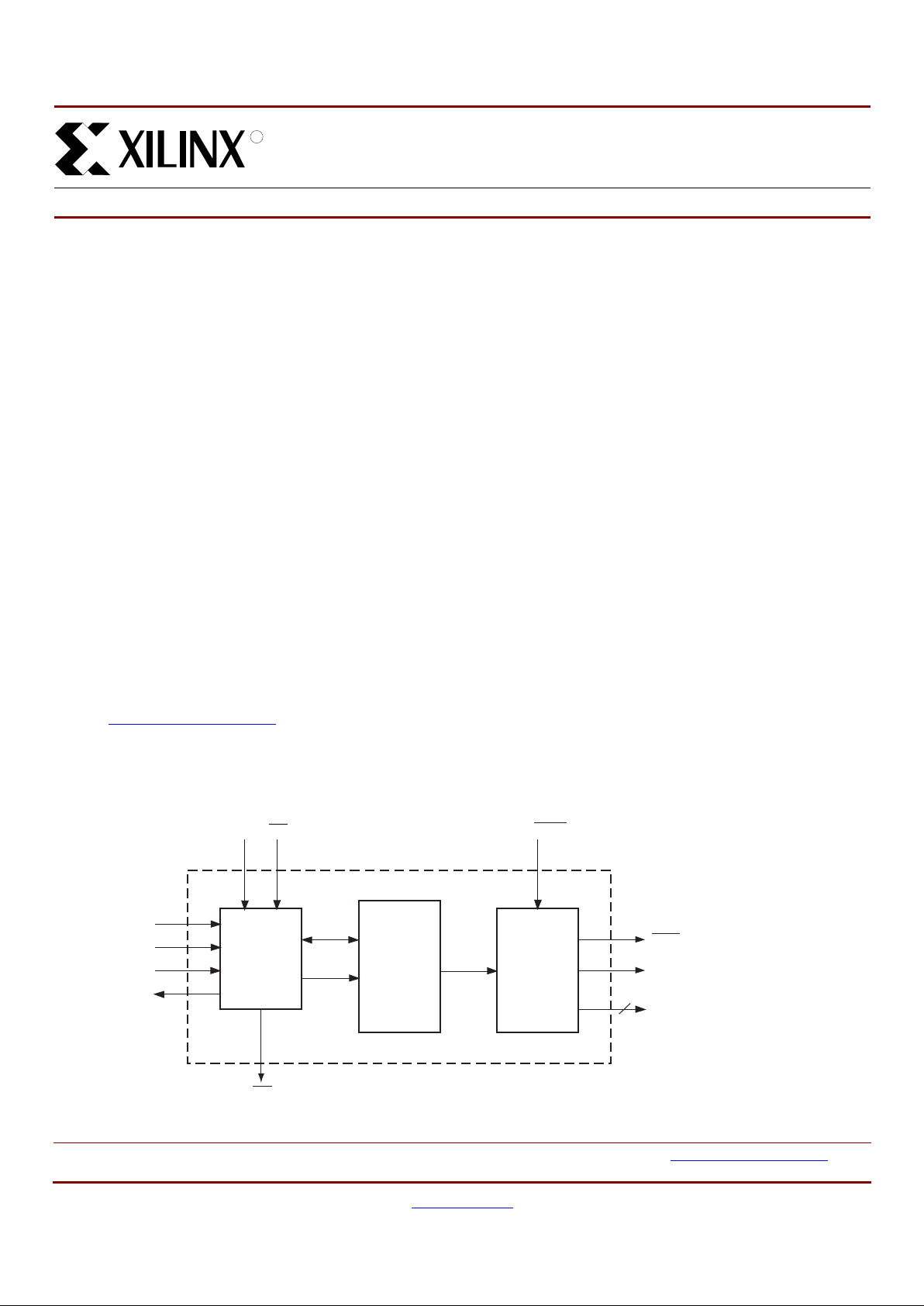
R
Figure 1: XQ18V04 Series Block Diagram
Control
and
JTAG
Interface
Memory
Serial
or
Parallel
Interface
D0 DATA
(Serial or Parallel
[Express/SelectMAP] Mode)
D[1:7]
Express Mode and
SelectMAP Interface
Data
Address
CLK
CE
TCK
TMS
TDI
TDO
OE/Reset
CEO
Data
DS026_01_021000
7
CF
Page 2
QPro XQ18V04 (XQR18V04) QML In-System Programmable Configuration PROMs
2 www.xilinx.com DS082 (v1.2) Nov em ber 5, 2001
1-800-255-7778 Preliminary Product Specification
R
Multiple devices can be concatenated by using the CEO
output to drive the CE input of the following device. The
clock inputs and the DATA outputs of all PROMs in this
chain are interconnected. All devices are compatible and
can be cascaded with other members of the family or with
the XC1700L one-time programmable Serial PROM family.
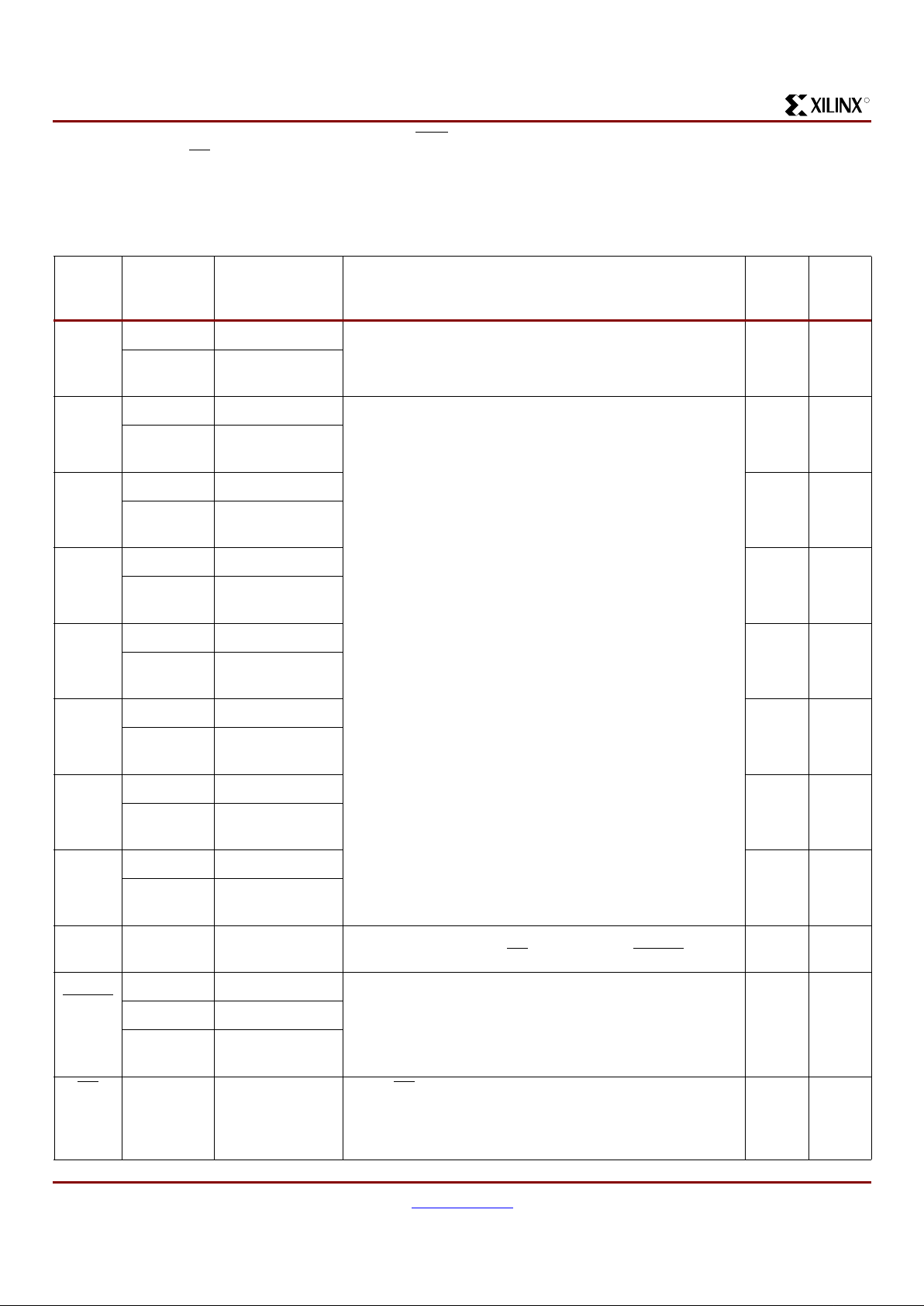
Pinout and Pin Description
Table 1: Pin Names and Descriptions (pins not listed are “no connect”)
Pin
Name
Boundary
Scan
Order Function Pin Description
44-pin
VQFP
44-pin
CLCC
D0 4 DAT A OUT D0 is the DAT A output pin to provide data for c onfiguring an
FPGA in serial mode.
40 2
3OUTPUT
ENABLE
D1 6 DATA OUT D0-D7 are the output pins to provide parallel data for
configuring a Xilinx FPGA in Express/SelectMap mode.
29 35
5OUTPUT
ENABLE
D2 2 DATA OUT 42 4
1OUTPUT
ENABLE
D3 8 DATA OUT 27 33
7OUTPUT
ENABLE
D4 24 DATA OUT 9 15
23 OUTP UT
ENABLE
D5 10 DATA OUT 25 31
9OUTPUT
ENABLE
D6 17 DATA OUT 14 20
16 OUTP UT
ENABLE
D7 14 DATA OUT 19 25
13 OUTP UT
ENABLE
CLK 0 DATA IN Each rising edge on the CLK input increments the internal
address counter if both CE
is Low a n d OE/RESET is High.
43 5
OE/
RESET
20 DATA IN When Low, this input holds the address counter reset and
the DATA output is in a high-impedance state. This is a
bidirectional open-drain pin that is held Low while the
PROM is reset. Polarity is NOT programmable.
13 19
19 DATA OUT
18 OUTP UT
ENABLE
CE
15 DATA IN When CE is High, this pin puts the device into standby
mode and resets the address counter. The DA T A output pin
is in a high-impedance state, and the device is in low power
standby mode.
15 21
Page 3
QPro XQ18V04 (XQR18V04) QML In-System Programmable Configuration PROMs
DS082 (v1.2) November 5, 2001 www.xilinx.com 3
Preliminary Product Specification 1-800-255-7778
R
CF 22 DATA OUT Allows JTAG CONFIG instruction to initiate FPGA
configuration without powering down FPGA. This is an
open-drain output that is pulsed Lo w by the JTAG CONFIG
command.
10 16
21 OUTP UT
ENABLE
CEO 13 DATA OUT Chip Enable Output (CEO
) is connected to the CE input of
the next PROM in the chain. This output is Low when CE
is
Low and OE/RESET
input is High, AND the internal
address counter has been incremented beyond its
Terminal Count (TC) value. When OE/RESET
goes Low,
CEO
stays High until the PROM is brought out of reset by
bringing OE/RESET
High.
21 27
14 OUTP UT
ENABLE
GND GND is the ground connection. 6, 18,
28 &
41
3, 12,
24 &
34
TMS MODE SELECT The state of TMS on the rising edge of TCK determines the
state transitions at the Test Access Port (TAP) controller.
TMS has an internal 50K ohm resistive pull-up on it to
provide a logic "1" to the device if the pin is not driven.
511
TCK CLOCK This pin is the JTAG test clock. It sequences the TAP
controller and all the JTAG test and programming
electronics.
713
TDI DATA IN This pin is the serial input to all JTAG instruction and data
registers. TDI has an internal 50K ohm resistive pull-up on
it to provi de a l ogi c "1" to th e syste m if the pin is not driv en.
39
TDO DAT A OUT This pin is the serial output f or all JTAG instruction and data
registers. TDO has an internal 50K ohm resistive pull-up on
it to provide a logic "1" to the system if the pin is not driven.
31 37
V
CC
Positive 3.3V supply voltage for internal logic and input
buffers.
17, 35
& 38
23, 41
& 44
V
CCO
Positive 3.3V or 2.5V supply voltage connected to the
output voltage drivers.
8, 16,
26 &
36
14, 22,
32 &
42
Table 1: Pin Names and Descriptions (pins not listed are “no connect”) (Continued)
Pin
Name
Boundary
Scan
Order Function Pin Description
44-pin
VQFP
44-pin
CLCC
Page 4
QPro XQ18V04 (XQR18V04) QML In-System Programmable Configuration PROMs
4 www.xilinx.com DS082 (v1.2) Nov em ber 5, 2001
1-800-255-7778 Preliminary Product Specification
R
Xilinx FPGAs and Compatible PROMs
Capacity
In-System Programming
In-System Programmable PROMs can be programmed individually, or two or more can be daisy-chained together and
programmed in-system via the standard 4-pin JTAG protocol as shown in Figure 2. In-system programming offers
quick and efficient design iterations an d eliminates unnecessary package handling or socketing of devices. The Xilinx
development system provides the programming data
sequence using either Xilinx JTAG Programmer software
and a download cable, a third-party JTAG dev elopment system, a JTAG-compatible board tester, or a simple microprocessor interface that emulates the JTAG instruction
sequence. The JTAG Programmer software also outputs
serial vector format (SVF) files for use with any tools that
accept SVF format and with automatic test equipment.
All outputs are held i n a high-impedance state or held at
clamp levels during in-system programming.
OE/RESET
The ISP programming algorithm requires issuance of a
reset that w ill c au s e OE to go Low.
External Programming
Xilinx reprogrammable PROMs can also be programmed by
the Xilinx HW-130 device programmer. This provides the
added flexibility of using pre-programmed d evices in board
design and boundary-scan manufacturing tools, with an
in-system programmable option for future enhancements
and design changes.
Reliability and Endurance
Xilinx in-system programmable p roducts provide a guaranteed endurance level of 2,000 in-system program/erase
cycles and a minimum data retention of ten years. Each
device meets all functional, performance, and data retention
specifications within this endurance limit.
Design Security
The Xilinx in-syst em programmab le PROM de vices incorporate advanced data security features to fully protect the programming data against unauthorized reading. Table 2
shows the security setting available.
The read security bit can be set by the user to prevent the
internal programming pattern f rom bei ng read or copied via
JTAG. When set, it a llows device erase. Erasing the entire
device is the only way to reset the read security bit.
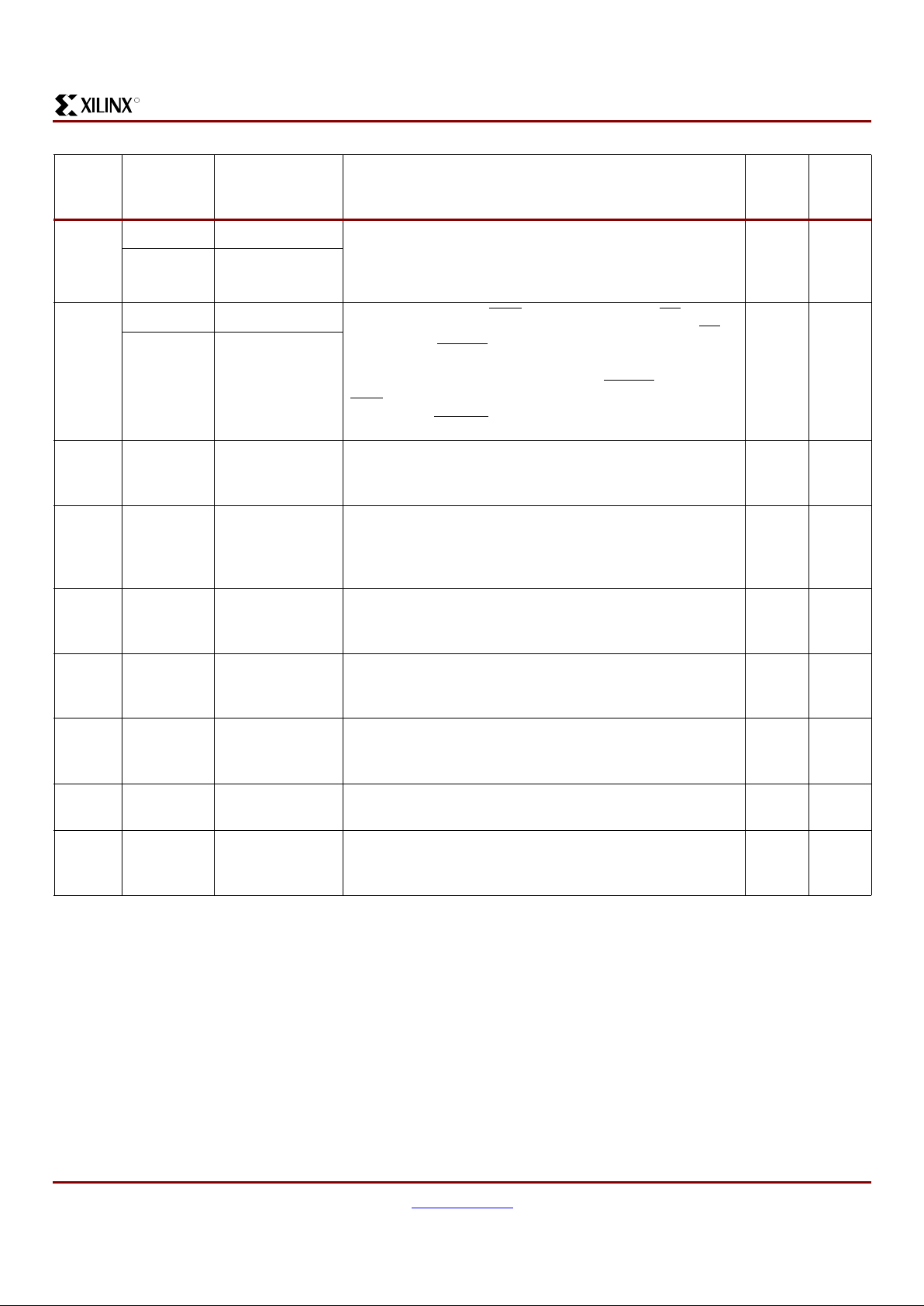
Table 2: Data Security Options
Device
Configuration
Bits
XQ(R)18VO4
PROMs
XQV100 781,216 1
XQV(R)300 1,751,808 1
XQV(R)600 3,607,968 1
XQV(R)1000 6,127,744 2
XQV(R)600E 3,961,632 1
XQV(R)1000E 6,587,520 2
XQV(R)2000E 10,159,648 3
Devices Configuration Bits
XQ(R)18V04 4,194,304
Default = Reset Set
Read Allowed
Program/Erase Allowed
Read Inhibited via JTAG
Erase Allowed
Page 5
QPro XQ18V04 (XQR18V04) QML In-System Programmable Configuration PROMs
DS082 (v1.2) November 5, 2001 www.xilinx.com 5
Preliminary Product Specification 1-800-255-7778
R
IEEE 1149.1 Boundary-Scan ( JTAG)
The XQ(R)18V0 4 famil y is fully com pliant wit h the IEEE Std.
1149.1 Boundary-Scan, also known as JTAG. A Test
Access Port (TAP) and regi sters are provided to s uppo rt all
required boundary scan instructions, as well as many of the
optional instructions specified by IEEE Std. 1149.1. In addition, the JTAG interf ace is used to imp lement in-syst em programming (ISP) to facilitate configuration, erasure, and
verification operations on the XQ(R)18V04 device.
Table 3 lists the required and optional boundary-scan
instructions supported in the XQ(R)18V04. Refer to the
IEEE Std. 1149.1 specificati o n for a complete descrip tion of
boundary-scan architecture and the required and optional
instructions.
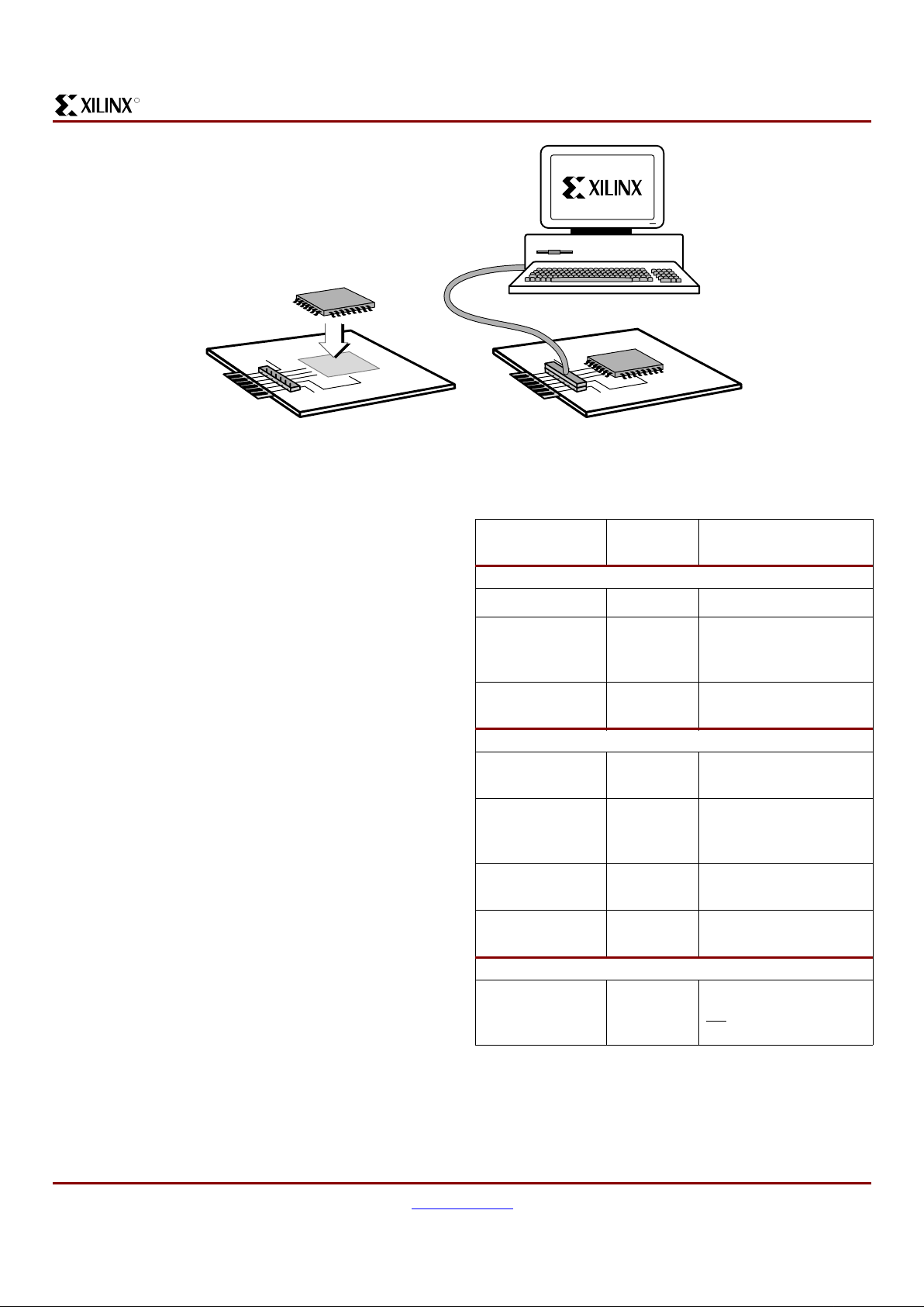
Figure 2: In-System Programming Operation (a) Solder Device to PCB and (b) Program Using Download Cable
DS026_02_011100
G
N
D
V
CC
(a) (b)
Table 3: Boundary Scan Instructions
Boundary-Scan
Command
Binary
Code [7:0] Description
Requ ired In s truc ti o ns
BYPASS 11111111 Enables BYP ASS
SAMPLE/
PRELOAD
00000001 Enables boundary-scan
SAMPLE/PRELOAD
operation
EXTEST 00000000 Enables boundary-scan
EXTEST operation
Optional Instructions
CLAMP 11111010 Enables boundary-scan
CLAMP operation
HIGHZ 11111100 All outputs in
high-impedance state
simultaneously
IDCODE 11111110 Enables shifting out
32-bit IDCODE
USERCODE 11111101 Enables shifting out
32-bit USERCODE
XQ(R)18V04 Specific Instructions
CONFIG 11101110 Initiates FPGA
configuration by pulsing
CF
pin Low
Page 6
QPro XQ18V04 (XQR18V04) QML In-System Programmable Configuration PROMs
6 www.xilinx.com DS082 (v1.2) Nov em ber 5, 2001
1-800-255-7778 Preliminary Product Specification
R
Instruction Register
The Instruction Register (IR) for the XQ(R)18V04 is eight
bits wide and is connected between TDI and TDO during an
instruction scan sequence. In preparation for an instruction
scan sequence, the instruction register is parallel loaded
with a fixed instruction capture pattern. This pattern is
shifted out onto TDO (LSB first), while an instruction is
shifted into the instructi on register from TDI. The detailed
compos ition of the instructi on captur e pattern is illustrat ed
in Figure 3.
The ISP Status field, IR(4), contains logic "1" if the device is
currently in ISP mode; otherwise, it will contain logic "0".
The Security field, IR(3 ), will contain logic "1" if th e device
has been programmed with the security option turned on;
otherwise, it will contain logic "0".
Boundary Scan Register
The boundary -s can register is used t o control and observe
the state of the device pins during the EXTEST, SAMPLE/PRELOAD, and CLAMP instructions. Each output pin
on the XQ(R)18V00 has two register stages that contribute
to the boundary-scan register, while each input pin only has
one register stage.
For each output pin, the register stage nearest to TDI c ontrols and observes the output state, and the second stage
closest to TDO controls and obser ves the High-Z enable
state of the pin.
For each input pin, the register stage controls and observes
the input state of the pin.
Identification Registers
The IDCODE is a fixed, vendor-assigned value that is used
to electrically identify the manufacturer and type of the
device being addressed. The IDCODE register is 32 bits
wide. The IDCODE register can be shifted out for examina-
tion by using the IDCODE instruction. The IDCODE is available to any other system component via JTAG.
The IDCODE register has the following binary format:
vvvv:ffff:ffff:aaaa:aaaa:cccc:cccc:ccc1
where
v = the die version number
f = the family code (50h for XQ(R)18V04 family)
a = the ISP PROM product ID (26h for the XQ(R)18V04)
c = the company code (49h for Xilinx)
Note: The LSB of the IDCODE register is always read as
logic "1" as defined by IEEE Std. 1149.1
Table 4 lists the IDCODE register values for the
XQ(R)18V00 devices. 0
The USERCODE instr uction gives access to a 32-bit user
programmable scratch pad typically used to supply information about the device’s programmed contents. By using t he
USERCODE instruction, a user-programmable identification code can be shifted out for exam ination. This code is
loaded into the USERCODE register during programming of
the XQ(R)18V04 device. If the device is blank or was not
loaded during programming, the USERCODE register will
contain FFFFFFFFh.
XQ(R)18V04 TAP Characteristics
The XQ(R)18V04 family performs both in-system programming and IEEE 1149.1 boundar y-sc an (JTAG) testing via a
single 4-wire Test Access P ort (TAP). This simplifies sys tem
designs and allows standard Automatic Test Equi pment to
perform both functions. The AC characteristics of the
XQ(R)18V04 TAP are descr ibed as follows.
TAP Timing
Figure 4 shows the timing relationships of the TAP signals.
These TAP timing characteristics are identical for both
boundary-s can and ISP operations.
IR[7:5] IR[4] IR[3] IR[2] IR[1:0]
TDI-> 0 0 0 ISP
Status
Security 0 0 1
->TDO
Notes:
1. IR(1:0) = 01 is specified by IEEE Std. 1149.1
Figure 3: Instruction Register Values Loaded into IR as
Part of an Instruction Scan Sequence
Table 4: IDCODES Assigned to XQ(R)18V04 Devices
ISP-PROM IDCODE
XQ(R)18V04 05026093h
Page 7

QPro XQ18V04 (XQR18V04) QML In-System Programmable Configuration PROMs
DS082 (v1.2) November 5, 2001 www.xilinx.com 7
Preliminary Product Specification 1-800-255-7778
R
TAP AC Parameters
Table 5 shows the timing parameters f or the TAP wavef orms
shown in Figure 4
Figure 4: Test Access Port Timing
TCK
T
CKMIN
T
MSS
TMS
TDI
TDO
T
MSH
T
DIH
T
DOV
T
DIS
DS026_04_020300
Table 5: T est Access Port Timing Parameters
Symbol Parameter Min Max Units
T
CKMIN1
TCK minimum clock period 100 - ns
T
CKMIN2
TCK minimum clock period, Bypass mode 50 - ns
T
MSS
TMS setup time 10 - ns
T
MSH
TMS hold time 25 - ns
T
DIS
TDI setup time 10 - ns
T
DIH
TDI hold time 25 - ns
T
DOV
TDO valid delay - 25 ns
Page 8

QPro XQ18V04 (XQR18V04) QML In-System Programmable Configuration PROMs
8 www.xilinx.com DS082 (v1.2) Nov em ber 5, 2001
1-800-255-7778 Preliminary Product Specification
R
Connecting Configuration PROMs
Connecting the FPGA device with th e configuration PROM
(see Figure 6).
• The DATA output(s) of the PROM(s) drives the D
IN
input of the lead FPGA device.
• The Master FPGA CCLK output drives the CLK input(s)
of the PROM(s) (in Master Serial mode only).
• The CEO
output of a PROM drives the CE input of the
next PROM in a daisy chain (if any).
• The OE/RESET
input of all PROMs is best dr iven by
the INIT
output of the lead FPGA device. This
connection assures that the PROM address counte r is
reset before the start of any (re)configuration, even
when a reconfiguration is initiated by a V
CC
glitch.
• The PROM CE
input can be driven from the DONE pin.
The CE
input of the first (or only) PROM can be driven
by the DONE output of the first FPGA device, provided
that DONE is not permanently grounded. CE
can also
be permanently tied Low, but this keeps the DATA
output active and causes an unnecessary supply
current of 20 mA maximum.
• Express/SelectMap mode is similar to slave serial
mode. The DATA is clocked out of the PROM one by te
per CCLK instead of one bit per CCLK cycle. See
FPGA data sheets for special configuration
requirements.
Initiating FPGA Configuration
The XQ(R)18V04 devices incorporate a pin nam ed CF that
is controllable through the JTAG CONFIG instruction. Executing the CONFIG instruction through JTAG pulses the CF
low for 300-500 ns, which resets the FPGA and initiates
configuration.
The CF
pin must be connected to the PROGRAM pin on the
FPGA(s) to use this feature.
The JTAG Programmer software can also issue a JTAG
CONFIG command to initiate FPGA configuration through
the "Load FPGA" setting.
Selecting Configuration Modes
The XQ(R)18V04 accomm odates serial and parallel m ethods of configuration. The configuration modes are selectable through a user control register in the XQ(R)18V04
device. This control register is accessible through JTAG,
and is set using the "Parallel mode" setting on the Xilinx
JT A G Program mer software. Serial output is the default programming mode.
Master Serial Mode Summary
The I/O and logic func tions of the Configurable Log ic Block
(CLB) and their associated interconnections are established
by a configuration program. The program is loaded either
automatically upon power up, or on command, depending
on the state of the three FPGA mode pins. In Master Serial
mode, the FPGA automatically loads the configuration program from an external memory. Xilinx PROMs are designed
to accommodate the Master Serial mode.
Upon power-up or reconfiguration, an FPGA enters the
Master Serial mode whenever all three of the FPGA
mode-select pins are Low (M0=0, M1=0, M2=0). Data is
read from the PROM sequentially on a single data line. Synchronization is provided by the rising edge of the temporary
signal CCLK, which i s gene rated by the FPGA during configuration.
Master Serial Mode provides a simple configuration interface. Only a serial dat a line, a clock line, and two control
lines are required to configure an FPGA. Data from the
PROM is read sequentially, accessed via the internal
address and bit count ers which are increment ed on every
valid rising edge of CCLK. If the user-programmable,
dual-function D
IN
pin on the FPGA is used only for configuration, it m ust st ill be held at a de fined level dur ing n orma l
operation. The Xilinx FPGA families take care of this automatically with an on-chip pu ll-up resist or.
Cascading Configuration PROMs
For multiple FPGAs configured as a serial daisy-chain, or a
single FPGA requir ing larger configuration memories in a
serial or SelectMAP configuration mode, cascaded PROMs
provide additional memory (Figure 5). Multiple XQ(R)18V04
devices can be concatenated by using the CEO
output to
drive the CE
input of the downstream device. The clock
inputs and the data outputs of all XQ(R)18V04 devices in
the chain are interconnecte d. Afte r the last bit from the first
PROM is read, the next clock signal to the PROM asserts its
CEO
output Low and drives its DATA line to a high-impedance state. The second PROM recognizes the Low level on
its CE
input and enables its DATA output. See Figure 6.
After configuration is complete, the address counters of all
cascaded PROMs are reset if the PROM OE/RESET
pin
goes Low.
Page 9

QPro XQ18V04 (XQR18V04) QML In-System Programmable Configuration PROMs
DS082 (v1.2) November 5, 2001 www.xilinx.com 9
Preliminary Product Specification 1-800-255-7778
R
Figure 5: JTAG Chain for Configuring Devices in Master Serial Mode
4.7K
**
1
2
3
4
TDO
DOUT
TDI
TMS
TCK
Vcc
Vcc
DIN
CCLK
DONE
INIT
Vcc MODE PINS*
Xilinx
FPGA
Master
Serial
Vcc
D0
Vcco
TDI CLK
TMS CE
TCK CEO
OE/RESET
PROGRAM
TDO
TDI
TMS
TCK
DIN
CCLK
DONE
INIT
Vcc MODE PINS*
Xilinx
FPGA
Slave
Serial
PROGRAMCF
TDO
GND
* For Mode pin connections, refer to appropriate FPGA data sheet.
** Virtex, Virtex-E is 300 ohms, all others are 4.7K.
XC18V00
Cascaded
PROM
TDI
TMS
TCK
TDO
J1
DS026_08_021000
VccVccoVcco
Vcc
D0
Vcco
TDI CLK
TMS CE
TCK CEO
OE/RESET
CF
TDO
GND
XC18V00
First
PROM
Vcc
Page 10

QPro XQ18V04 (XQR18V04) QML In-System Programmable Configuration PROMs
10 www.xilinx.com DS082 (v1.2) Nov em ber 5, 2001
1-800-255-7778 Preliminary Product Specification
R
Figure 6: (a) Master Serial Mode (b) Virtex Select MAP Mode (c) Spartan-XL Express Mode
(dotted lines indicates optional connection)
PROGRAM
DIN
CCLK
INIT
DONE
First
PROM
DATA
CEO
CLK
CE
OPTIONAL
Slave FPGAs
with identical
configurations
Vcc
FPGA
(Low Resets the Address Pointer)
VCCV
CCO
OPTIONAL
Daisy-chained
FPGAs with
different
configurations
OE/RESET
DOUT
Modes*
Vcco
CF
PROGRAM
VIRTEX
Select MAP
BUSY
CS
WRITE
INIT
D[0:7]
CCLK
DONE
CLK
Virtex Select MAP Mode
D[0:7]
CE
OE/RESET
XC18Vxx
Modes***
NC
CF
3.3V
External Osc
CEO
4.7K
V
CC
4.7K
V
CC
**
**
VCCV
CCO
VCCV
CCO
V
CC
4.7K
V
CC
4.7K
V
CC
1K
I/O*
M0
M1
CS1
PROGRAM
Spartan-XL,
XC4000
DOUT
DONE
INIT
XC18Vxx
CEO
CE
OE/RESET
Spartan-XL Express Mode
Master Serial Mode
8
CF
CLK
D[0:7]
D[0:7]
CCLK
M0
M1
CS1
PROGRAM
Optional
Daisy-chained
Spartan-XL,
XC4000
DOUT
DONE
INIT
D[0:7]
CCLK
8
To Additional
Optional
Daisy-chained
Devices
To Additional
Optional
Daisy-chained
Devices
External Osc
I/O*
1K
*CS and WRITE must be pulled down to be used as I/O. One option is shown.
**Virtex, Virtex-E is 300 ohms, all others are 4.7K.
***For Mode pin connections, refer to the appropriate FPGA data sheet.
DS026_05_031000
*For Mode pin connections, refer to the appropriate FPGA data sheet.
**Virtex, Virtex-E is 300 ohms, all others are 4.7K.
Cascaded
PROM
DATA
CLK
CE
OE/RESET
CF
VCCV
CCO
VCCV
CCO
V
CC
Page 11

QPro XQ18V04 (XQR18V04) QML In-System Programmable Configuration PROMs
DS082 (v1.2) November 5, 2001 www.xilinx.com 11
Preliminary Product Specification 1-800-255-7778
R
5V Tolerant I/Os
The I/Os on each re-programmable PROM are fully 5 V tolerant even through the core power supply is 3.3V. This
allows 5V CMOS signals to connect directly to the PROM
inputs without damage. In addition, the 3.3V V
CC
power
supply can be applied before or after 5V signals are applied
to the I/Os. In mixed 5V/3.3V/2.5V system s, the user pins,
the core power supply (V
CC
), and the output power supply
(V
CCO
) may have power applied in any order. This makes
the PROM devices immune to power supply sequencing
issues.
Reset Activation
On power up, OE/RESET is held low until the XQ(R)18V04
is active (1 ms) and able to supply data after receiving a
CCLK pulse from the FPGA. OE/RESET
is connected to an
external resistor to pull OE/RESET
HIGH releasing the
FPGA INIT
and allowing configuration to begin. OE/RESET
is held low until the XQ(R)18V04 voltage reaches the operating voltage range. If the power drops below 2.0V, the
PROM will res et. OE/RESET
polarity is NOT programma-
ble.
Standby Mode
The PROM enters a low-power standby mode whenever CE
is asserte d High. The output remains in a high-impedanc e
state regardless of the state of the OE input. JTAG pins
TMS, TDI and TDO c an be in a high-impedance state or
High.
Customer Control Pins
The XQ(R)18V04 PROMs have various control bits accessible by the customer. These can be set after the array has
been programmed using " Skip User Array" in Xilinx JTAG
Programmer Software.
Table 6: Truth Table for PROM Control Inputs
Cont ro l Inpu t s
Internal Address
Outputs
OE/RESET CE DATA CEO I
CC
High Low If address < TC
(1)
: increment
If address > TC
(1)
: don’t change
Active
High-Z
High
Low
Active
Reduced
Low Low Held reset High-Z High Act ive
High High Held reset High-Z High Standby
Low High Held reset High-Z High Standby
Notes:
1. TC = Terminal Count = highest add ress value. TC + 1 = address 0.
Page 12

QPro XQ18V04 (XQR18V04) QML In-System Programmable Configuration PROMs
12 www.xilinx.com DS082 (v1.2) Nov em ber 5, 2001
1-800-255-7778 Preliminary Product Specification
R
Absolute Maximum Ratings
(1,2)
Recommended Operating Conditions
Quality and Reliability Characteristics
Radiation Tolerances for XQR18V04
Symbol Description Value Units
V
CC
Supply voltage relative to GND –0.5 to +4.0 V
V
IN
Input voltage with respect to GND –0.5 to +5.5 V
V
TS
Voltage appl ied to High-Z output –0.5 to +5.5 V
T
STG
Storage temperature (ambient) –65 to +150 °C
T
J
Junction temperature Ceramic +150 °C
Plastic +125 °C
Notes:
1. Maximum DC under shoot be low G ND must be limi ted t o eit her 0.5 V or 10 mA, whi che v er is easi er t o achieve. During transiti ons, the
device pi ns may undershoot to –2.0V or overshoot to +7.0V, provided this over- or undershoot lasts less then 10 ns and with the
forcing current being limited t o 200 mA.
2. Stresses beyond those listed under Absolute Maximum Ratings may cause permanent damage to the device. These are stress
ratings on ly, and functional operat ion of the device at these or any other condit ions beyond those listed under Ope rating Conditions
is not implied. Exposure to Absolute Maximum Ratings conditions for ext ended periods of time may affect device reliabili ty.
Symbol Parameter Min Max Units
V
CCINT
Internal voltage supply (TC = –55°C to +125°C) Ceramic 3.0 3.6 V
Internal voltage supply (T
J
= –55°C to +125°C) Plastic 3.0 3.6 V
V
CCO
Supply voltage for output drivers for 3.3V operation 3.0 3.6 V
Supply voltage for output drivers for 2.5V operation 2.3 2.7 V
V
IL
Low-level input voltag e 0 0.8 V
V
IH
High-level input voltage 2.0 5.5 V
V
O
Output voltage 0 V
CCO
V
Symbol Description Min Max Units
T
DR
Data retention 10 - Years
N
PE
Program/erase cycles (Endurance) 2,000 - Cycles
V
ESD
Electrostatic discharge (ESD) 2,000 - Volts
Symbol Description Min Max Units
TID T otal Ionizing Dose - 40 krad(Si)
SEL Single Event Latch-Up
(No Latch-Up observed for LET > 120 MeV -mg/cm
2
)
-0cm
2
SEU Static Memo ry Cell Saturation Bit Cross-Section
(No Upset observed for LET > 120 MeV-m g/cm
2
)
-0cm
2
Page 13

QPro XQ18V04 (XQR18V04) QML In-System Programmable Configuration PROMs
DS082 (v1.2) November 5, 2001 www.xilinx.com 13
Preliminary Product Specification 1-800-255-7778
R
DC Characte ri sti cs Over Operat ing Con dit ions
Symbol Parameter Test Conditions Min Max Units
V
OH
High-level output voltage for 3.3V outputs IOH = –4 mA 2.4 - V
High-level output voltage for 2.5V outputs I
OH
= –500 µA 90% V
CCO
-V
V
OL
Low-lev el output voltage for 3.3V outputs IOL = 8 mA - 0.4 V
Low-lev el output voltage for 2.5V outputs I
OL
= 500 µA-0.4V
I
CC
Supply current, active mode 25 MHz - 50 mA
I
CCS
Supply current, standby mode - 20 mA
I
ILJ
JTAG pins TMS, TDI, and TDO V
CC =
MAX
V
IN
= GND
–100 - µA
I
IL
Input leakage current V
CC
= Max
V
IN
= GND or V
CC
–10 10 µA
I
IH
Input and output High-Z leakage current V
CC
= Max
V
IN
= GND or V
CC
–10 10 µA
C
IN
and
C
OUT
Input and output capacitance VIN = GND
f = 1.0 MHz
-10pF
Page 14

QPro XQ18V04 (XQR18V04) QML In-System Programmable Configuration PROMs
14 www.xilinx.com DS082 (v1.2) Nov em ber 5, 2001
1-800-255-7778 Preliminary Product Specification
R
.AC Characteristics Over Operating Conditions for XC18V04 .
Symbol Description Min Max Units
T
OE
OE/RESET to data delay - 10 ns
T
CE
CE to data delay - 20 ns
T
CAC
CLK to data delay - 20 ns
T
OH
Data hold from CE, OE/RESET, or CLK 0 - ns
T
DF
CE or OE/RESET to data float delay
(2)
-25ns
T
CYC
Clock periods 50 - ns
T
LC
CLK Low time
(3)
10 - ns
T
HC
CLK High time
(3)
10 - ns
T
SCE
CE setup time to CLK (to guarantee proper counting)
(3)
25 - ms
T
HCE
CE High time (to guarantee proper counting) 2 - µs
T
HOE
OE/RESET hold time (guarantees counters are reset) 25 - ns
Notes:
1. AC test load = 50 pF.
2. Float dela ys are measured with 5 pF AC loads. Transition is measured at ±200 mV from steady state activ e levels.
3. Guaranteed by design, not tested.
4. All AC parameters are measured with V
IL
= 0.0V and VIH = 3.0V.
5. If T
HCE
High < 2 µs, TCE = 2 µs.
OE/RESET
CE
CLK
DATA
T
CE
T
OE
T
LC
T
SCE
T
HCE
T
HOE
T
CAC
T
OH
T
DF
T
OH
T
HC
DS026_06_012000
T
CYC
Page 15

QPro XQ18V04 (XQR18V04) QML In-System Programmable Configuration PROMs
DS082 (v1.2) November 5, 2001 www.xilinx.com 15
Preliminary Product Specification 1-800-255-7778
R
AC Characteristics Over Operating Conditions When Cascading for XC18V04
Symbol Description Min Max Un its
T
CDF
CLK to data float delay
(2,3)
-25 ns
T
OCK
CLK to CEO delay
(3)
-20 ns
T
OCE
CE to CEO delay
(3)
-20 ns
T
OOE
OE/RESET to CEO delay
(3)
-20 ns
Notes:
1. AC test load = 50 pF.
2. Float dela ys are measured with 5 pF AC loads. Transition is measured at ±200 mV from steady
state active levels.
3. Guaranteed by design, not tested.
4. All AC parameters are measured with V
IL
= 0.0V and VIH = 3.0V.
CLK
DATA
CE
CEO
First Bit
Last Bit
T
CDF
DS026_07_020300
OE/RESET
T
OCK
T
OOE
T
OCE
Page 16

QPro XQ18V04 (XQR18V04) QML In-System Programmable Configuration PROMs
16 www.xilinx.com DS082 (v1.2) Nov em ber 5, 2001
1-800-255-7778 Preliminary Product Specification
R
Ordering Information
XQ18V04 CC44 V
Grade (Manufacturing Flow /
Temperature Range )
Device Number
Package Type
Device Ordering Options
Devi ce Type Package Grad e
XQ18V04 CC44 44-pin Ceramic Chip Carrier Package
M
Military Ceramic TC = –55°C to +125°C
XQR18V04
(1)
VQ44 44-pin Plastic Thin Quad Flat Package
N
Military Plastic TJ = –55°C to +12 5 °C
V
QPro-Plus TC = –55°C to +125°C
Notes:
1. Radiation Hardened.
5962 - 01525 Q Y A
Lead Finish
Generic Standard
Microcircuit Drawing (SMD)
Radiation Hardened
(1)
Package Type
QML Certified MIL-PRF-3 8535
SMD Ordering Options
Device Type QML
Package
Lead Finish
5962-01525 XQ18V04 - 44-pin Ceramic Chip Carrier Package Solder Dip
5962R01525 XQR18V04 - 44-pin Plastic Thin Quad Flat Package Solder Plate
Notes:
1. Type R designates Radiation Hardened.
Valid Ordering Combinations
Mil-Std SMD Rad Hard SMD
XQ18V04CC44M
-
XQR18V04CC44M
-
XQ18V04VQ44N - XQR18V04CC44V
Device Type
Page 17

QPro XQ18V04 (XQR18V04) QML In-System Programmable Configuration PROMs
DS082 (v1.2) November 5, 2001 www.xilinx.com 17
Preliminary Product Specification 1-800-255-7778
R
Revision History
The following table shows the revision history for this document.
Date Version Revision
5/1/01 1.0 First publication of this early access specification
7/23/01 1.1 Preliminary publication supporting Full Mil Temp range and corrected write cycles
11/05/01 1.2 Added Class V to ordering combinations for Rad Hard version. Updated format.
 Loading...