

Page 1
FCC Registered DAA Module with DTMF Transmitter/Decoder
XE0068DT
2/99
Description
The XE0068DT is an FCC registered telephone line
interface which includes a DTMF transmitter, DTMF
decoder and call progress monitor.
FCC rules limit the signal level that equipment can
place on the telephone line. The XE0068DT incorporates an Automatic Gain Control (AGC) circuit to control the output signal level. The AGC optomizes the
output levele over a wide variety of input levels without introducing signal distortion.
FCC rules also dictate a 2-second delay at the start of
each call. This billing delay prevents information
transmission during the billing period. The
XE0068DT includes this billing delay.
The integrated DTMF transceiver, call progress monitor and FCC registration make the XE0068DT ideal
for network signalling applications.
Features
* Small Size - 2.28" x 1.08" x 0.42"
* FCC Part 68 Registered
* Ring Detection and Hookswitch Control
* 1500 Volt Isolation;
* 800 Volt Surge Protection;
* An Integral 2-Second Billing Delay
* Auotomatic Gain Control optimizes transmit level
for most any input level.
* Integral DTMF transmitter and decoder
* Call progress Monitor
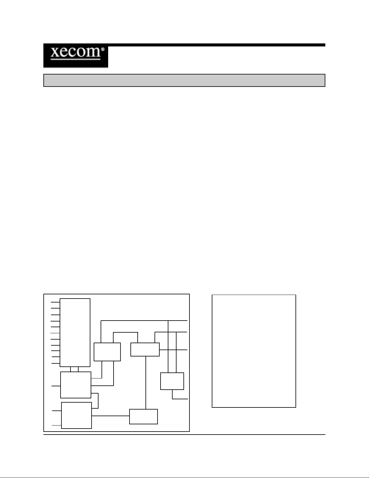
XE0068DT Block Diagram
D0
D1
D2 DTMF
D3 Transmitter Tip
ESt & Receiver
/RD Ring
/WR
/CS
RS0 Line Hook Switch OH
CP Transformer
StGT
XE0068DT Pin Configuration
VCC o 1 26 o Tip
D3 o 2
D2 o 3 24 o Ring
D1 o 4
D0 o 5 22 o /RI
/WR o 6 21 o OH
/RD o 7 20 o N/C
/CS o 8 19 o RCVR
RS0 o 9 18 o XMIT
RCVR Convertor Detect
2-4 Wire Ring
N/C o10 17 o StGT
N/C o 11 16 o ESt
N/C o 12 15 o CP
/RI
D/V o 13 14 o GND
XMIT
D/V Timer
AGC Billing Delay
XECOM (1) XE0068DT
Page 2
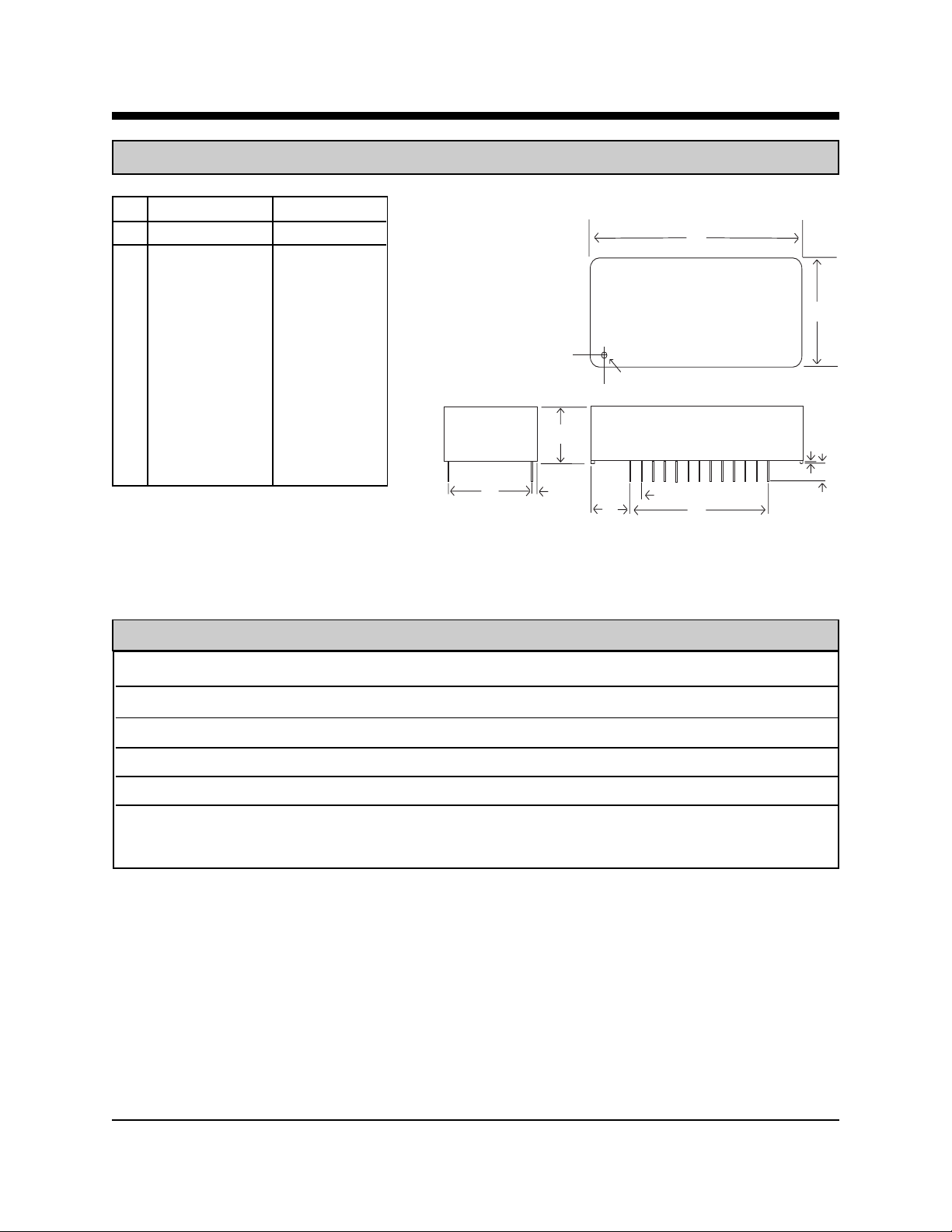
XE0068DT Mechanical Specifications
Inches Metric(MM)
Dim Min Max Min Max
A 2.270 2.290 57.66 58.17
B 1.065 1.095 27.05 27.81
C 0.420 0.430 12.32 13.08
D 0.890 0.910 22.61 23.11
E 1.190 1.210 30.23 30.73
F 0.125 0.200 3.18 5.08
G 0.080 0.100 2.03 2.54
H 0.530 0.550 13.46 13.97
J 0.090 0.110 2.29 2.79
K 0.020 0.025 0.51 0.64
D
G
C
Denotes Pin 1
J
H
A
B
K
E
F
XE0068DT ABSOLUTE MAXIMUM RATINGS
Storage T emperature -25O C to +85O C
Operating T emperature Range * 0O C to +70O C
Maximum Solder T emperature 220O C
Maximum Time Above Eutectic (183O C) 90 seconds
Preheat Dwell Time 120 to 180 seconds
* The XEV90 can be ordered with an Operating Temperature of -40O C to +85O C at extra cost.
Specify Industrial T emperature Range (ITR).
XECOM (2) XE0068DT
Page 3
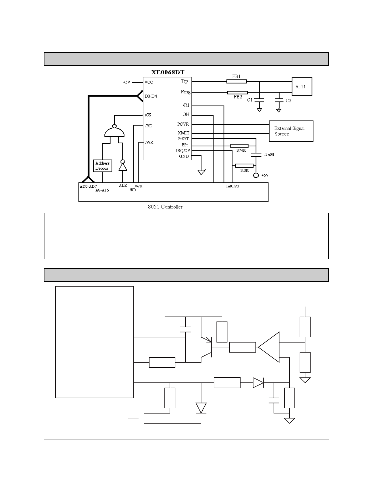
XE0068DT Typical Connection Diagram
Recommended Parts
Designation Description
C1, C2 47 picoFarad, 3000 Volts (Sprague part Number 30GA-T47
FB1, FB2 Ferrite Beads (TDK part Number CB30-453215B)
XE0068DT Call Progress Detection Circuit
XE0068DT
5volts
St/GT
ESt
CP
5volts
.1ufd
2N2907
374K
3K
1N4148
10K
150K
10K
5volts
10K
LM339
-
+
10K
1N4148
1M
.15 ufd
to IRQ
XECOM (3) XE0068DT
Page 4

XE0068DT Pin Descriptions
PIN NAME I/0 DESCRIPTION
1 VCC --- +5 Volts
2-5 D0-D3 I/O These singals represent the 4-bit data bus which carries the DTMF information per
the chart below.
6 WR I Read and Write determine the direction of DTMF data. A low on WR with RD high
allows the processor to write to the XE0068DT.
7 RD I Read and Write determine the direction of DTMF data. A low on RD with WR low
allows the processor to read from the XE0068DT.
8 CS I A low on Chip Select, selects the XE0068 DTMF data bus.
9 RS0 I This input selects the register to be used. A low selects the data register.
13 D/V I A low on Voice/Data selects a transmit level of 0 dBm for voice or DTMF; a high
sets a -9 dbm transmit level for data transfer.
14 GND --- Ground
15 CP O In DTMF mode CP acts as an interrupt. CP goes low when a valid DTMF Tone is
transmitted or received. In CallProgress Mode CP provides a square wave representation of the call progress signal on the phone line.
16 ESt O Goes high to indicate that a valid tone pair has been detected. A momentary loss of
signal causes ESt to go low.
17 St/GT I/O As an input, ST/GT latches the DTMF code into the Receive Data Register when
the threshold voltage is reached. As an output, St/GT goes high to disable the
guard timer after the threshold voltage is reached.
18 XMIT I Analog input signal to the line interface, input impedance on XMIT is typically 10
Kohms at 1800 Hz. Signals from -15 to +5 dBm will be placed on the line at 10dBm + 1 dBm.
19 RCVR O Analog output signal from the 2-4 wire converter, the output impedence of RCVR
is typically 10 ohms at 1800 hz.
21 OH I Hookswitch control. A high closes the internal relay to connect the equipment to
the phone line.
22 RI O Ring Indicate, output, active low, TTL, indicates the modem is receiving a ring sig-
nal.
24 Ring --- Ring connection to the phone line (RJ11 Pin 4).
26 Tip --- Tip Connection to the phone line (RJ11 Pin 3)
XECOM (4) XE0068DT
Page 5
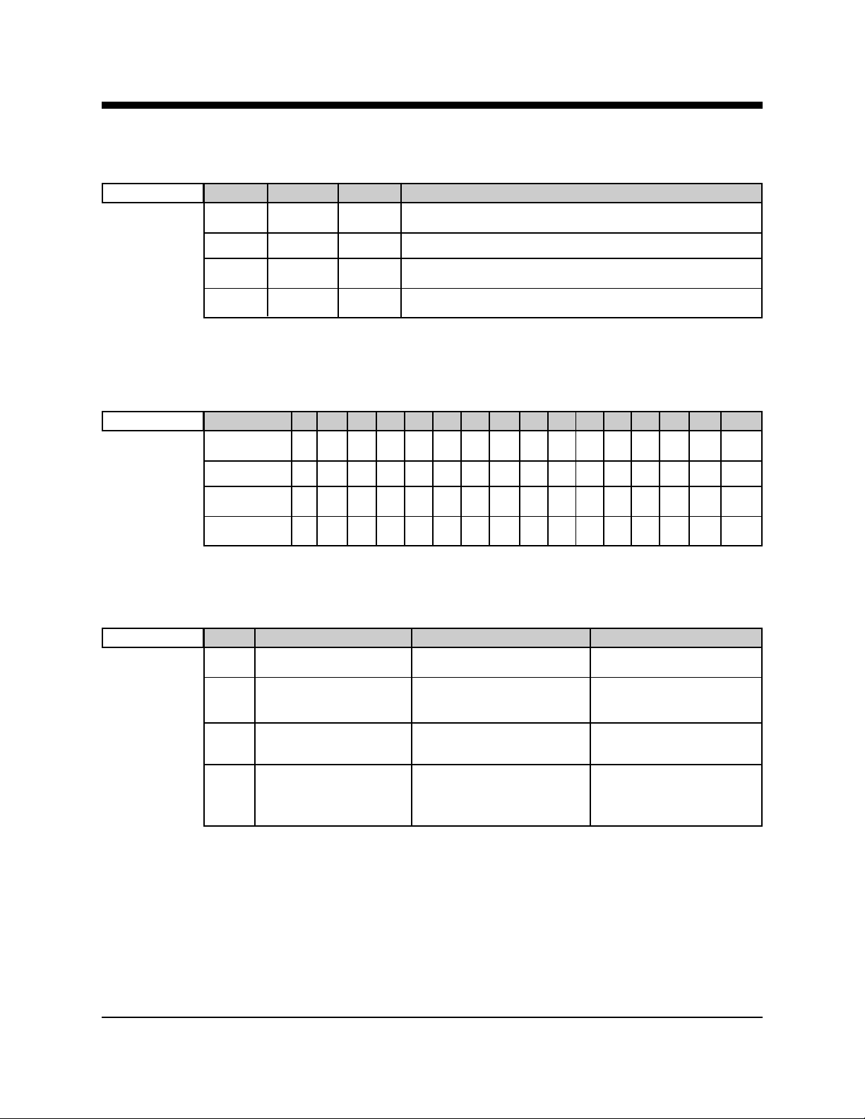
XE0068DT Register Selection
T able 1 below shows the combination of RS0, /WR, and /RD to select each register.
Table 1 RS0 /WR /RD Function
0 0 1 Write to Transmit Data Register
0 1 0 Read from Receive Data Register
1 0 1 Write to Control Register A or B
1 1 0 Read from Status Register
DTMF Codes
T able 2 below shows the 4-bit codes applied to D0-D3 to represent each DTMF Digit.
Table 1 DTMF Digit 1 2 3 4 5 67890*#ABCD
D0 101010101010101 0
D1 011001100110011 0
D2 000111100001111 0
D3 000000011111111 0
XE0068DT Status Register
T able 3 below defines the bit codess which can be read from the status register.
Table 3 Bit Indicator Status Set Status Cleared
0 IRQ An interrupt has occurred Interupt Active
1 Transmit Data Register Transmitter Ready for Status has been read or
Empty New Data is in non-burst mode
2 Receive Data Register ReceiveData Register Status Register has been
Full contains valid data Read
3 Delayed Steering Set upon detection Cleared upon detection of
of the absence of a a vailid DTMF signal
DTMF signal
XECOM (5) XE0068DT
Page 6
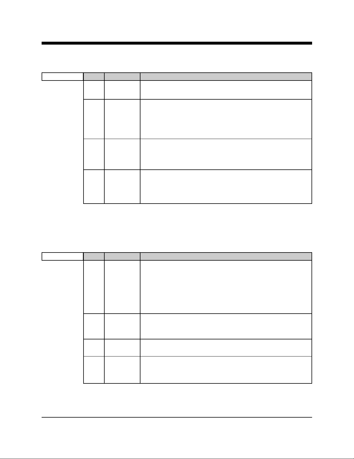
XE0068DT Control Register A
T able 4 below defines the XE0068DT operations set by the bits in Control Register A.
Table 4 Bit Signal Function
0 TOUT Tone Output Control: This bit controls the tone transmit functions. A
high enables the tone output; a low turns tone outputoff.
1 CP/DTMF Call Progress or DTMF Mode: A logic high enables the XE0068DT to
detect call progress tones. A low enables DTMF send and receive
mode. In call progress mod a square wavee representation of the
incoming signal will be presented on the CP output, IRQ enabled.
DTMF tones cannot be decoded in call progress mode.
2 IRQ Interrupt Enaable: A logic high enables the interrupt function. When
IRQ and DTMF mode are disabled, the CP output will go low when
either a valid DTMF signal is received or the transmitter is ready for
more data.
3 RSEL Register Select. A logic high on bit 3 sets the XE0068DT to select
Control Register B for the next write cycle. After writing to Control
Register B, the next control register write cycle will be directed to
Control Register A.
XE0068DT Control Register B
T able 5 below defines the XE0068DT operations set by the bits in Control Register B.
Table 4 Bit Signal Function
0 Burst Burst Mode: A logic low enables burst mode. When Burst Mode is
activated, DTMF tones can be transmitted by writing the correct code to
the Transmit Register. The XE0068DT the transmits a tone burst of 51
milliseconds on and 51 milliseconds off. In call progress mode the
duration of the tone burst and pause after the tone burst are doubled to
102 milliseconds. When not in Burst Mode the XE0068DT transmits
the tone as long as TOUT, Status Register A, is active.
1 Test Test Mode: A logic high enables the Test Mode in teh XE0068DT .
When the T est and DTMF modes are selected, the signal on CP reflects
the state of the delayed steering bit of the status register.
2 S/D Single or Dual Tone Generation: A logic high sets the XE0068DT to
generate a single tone rather than the transmiting two tones.
3 C/R Column or Row: Control Register B bit 3 determines if the row or
column tone is transmitted when single tone operation is selected. A
logic high selects the trow tone output
XECOM (6) XE0068DT
Page 7

XE0068DT Operational Modes
Burst Mode Burst mode is used to transmit DTMF signals of specific duration. The XE0068DT transmitter
sends symmetric tone bursts which are on for 51 milliseconds and off for 51 milliseconds. This
is a standard interval for central office switching. When call progress mode is also selected extended bursts of 102 milliseconds can be sent.
Single Tone Generation Single tones , rather than tone pairs , may also be generated. Control Register B regulates
single tone transmission.
Call Progress Mode Call Progress Mode allows detection of the various tones used to identify the status of a call.
They include Ring Back, Busy Tone Dial Tone, etc. In call Progress Mode the XE0068DT provides a square wave representation of these signals on the CP pin. The system host can decode
the incoming call progress tones.
Initialization Procedure
Description Control Lines Data Bits
RS0 WR RD B3 B2 B1 B0
Read Status Register 1 1 0 XXXX
Write to Control Register 1 0 1 0000
Write to Control Register 1 0 1 1000
Write to Control Register 1 0 1 0000
Write to Control Register 1 0 1 0000
* Performs a software reset on the XE0068DT
Call Progress Tone Definitions
The chart below shows the signal characteristics for the most common call progress tones in the United States.
Check the frequency and cadence on the CP line to identify signals in Call Progress mode.
Tone Frequency (Hz) Cadence Level Description
Dial Tone 350 + 400 Steady -13 dBm Indicates the network is ready to receive dialing
signals
Ringback 440 + 480 2 sec. On -19 dBm Indicates the called line is ringing
4 sec. Off
Busy T one 480 + 620 .5 sec. On -24 dBm Indicates the called line has been reached but is
.5 sec Off currently in use.
Reorder 480 + 620 .25 sec. On -24 dBm Indicates the switching path is busy
.25 sec Off
Partial Dial Tone 480 Steady -17 dBm Notifies the calling party that dialing has not begun
in the allotted time or that not enough digits have
been dialed.
XECOM (7) XE0068DT
Page 8
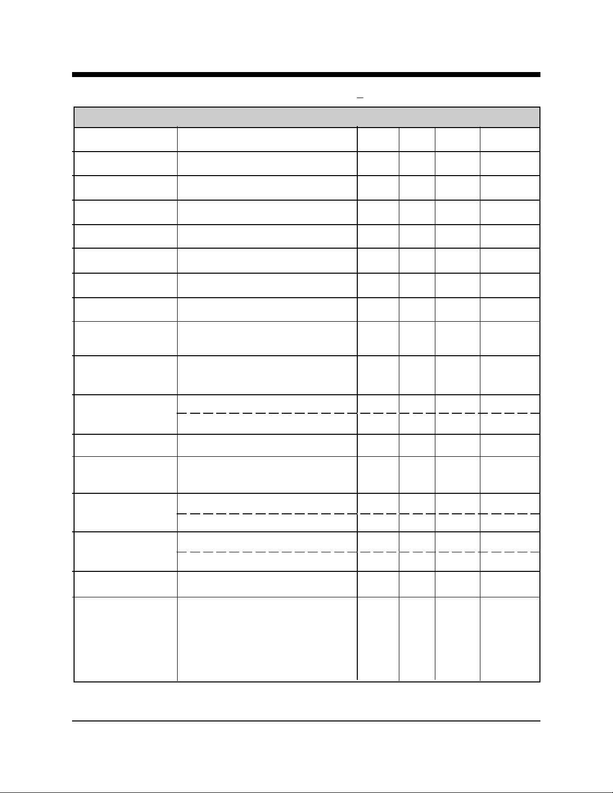
XE0068DT Electrical Specifications (Vcc = +5 Volts + 5%, Ta = 70 deg C.)
Parameter Conditions Min Typ Max Units
Power Supply Current Ring Indicate Active 20 mA
Coupler Match Output impedance of external 531 536 541 ohms
AGC Input Range Maintaining steady output level -40 0 dBm
AGC Output Level D/V held high -20 -9 dBm
AGC Output Level D/V held low -11 0 dBm
Billing Delay OH activated 2.0 2.3 seconds
Transhybrid Loss at 1000 Hz 34 dBm
Receive Loss at 1000 Hz -1.0 0 1.0 dB
Ring Detect Min. AC voltage between Tip & Ring 38 vrms
Sensitivity Type B ringer
Ring Indicate Ring Voltage present on Tip & Ring 0.2 0.5 volts
Output Voltage
Loop Current Switch ON: (off-hook) Control Voltage 2.0 3.0 volts
control voltage OFF: (on-hook) 0.2 0.5 volts
Loop Current Switch Off-hook Control Current 0.1 2.0 mA
Loop Current OFF-Hook current draw from 0 20 100 mA
Telephone Line
Data Bus, Low Level Input Voltage 0.8 volts
High Level Input Voltage 2.0 volts
Receive Sensitivity DTMF tones -37 dBm
Call Progress Tones -30 dBm
T one Duration to Detect 40 msec
Tone Frequencies DTMF Transmission, 697 hz
770
852
941
1209
1336
XECOM (8) XE0068DT
Page 9
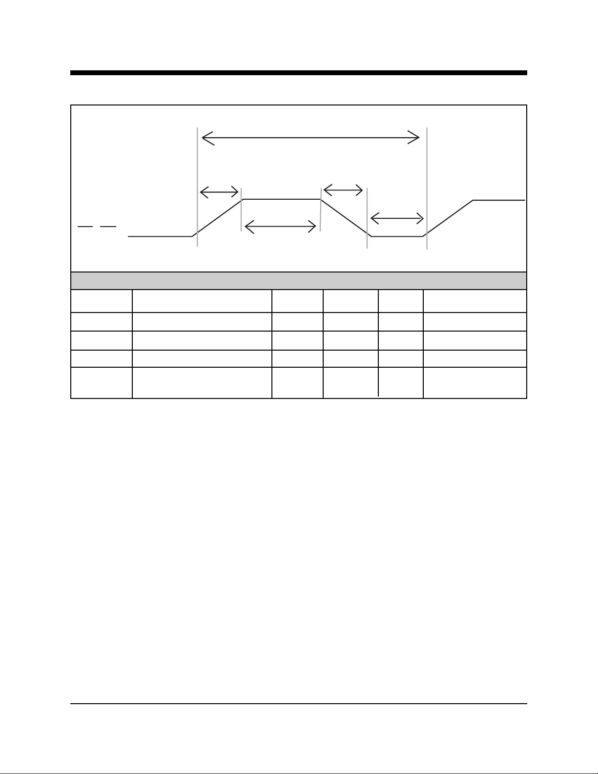
XE0068DT Read/Write Clock Pulse Timing
T
CYC
T
T
R
T
PWH
RD/WR
Signal Definition Min Typ Max Units
TR Read/Write Rise Time 20 nanoseconds
TF Read/Write Fall Time 20 nanoseconds
TCYC Read/Write Cycle period 250 nanoseconds
TRWH Read/Write pulse width high 100 nanoseconds
F
T
PWL
TPWL Read/Write pulse width low 150 nanoseconds
XECOM (9) XE0068DT
Page 10
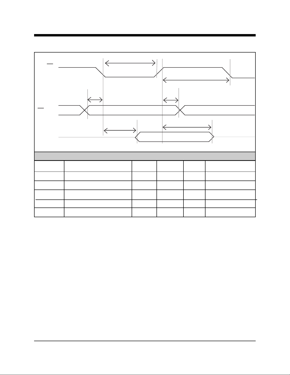
XE0068DT Read Timing
RD
T
PWL
T
PWH
T
AS
T
AH
CS, RSO
T
DHR
DATA BUS
T
DDR
Signal Definition Min Typ Max Units
TAS Address Setup Time 23 nanoseconds
TAH Address Hold Time 26 nanoseconds
TPWH Read Pulse Width High 100 nanoseconds
TPWL Read Pulse Width Low 150 nanoseconds
TDDR Read to Valid Data 100 nanoseconds
TDHR Data Hold Time (Read) 22 nanoseconds
XECOM (10) XE0068DT
Page 11
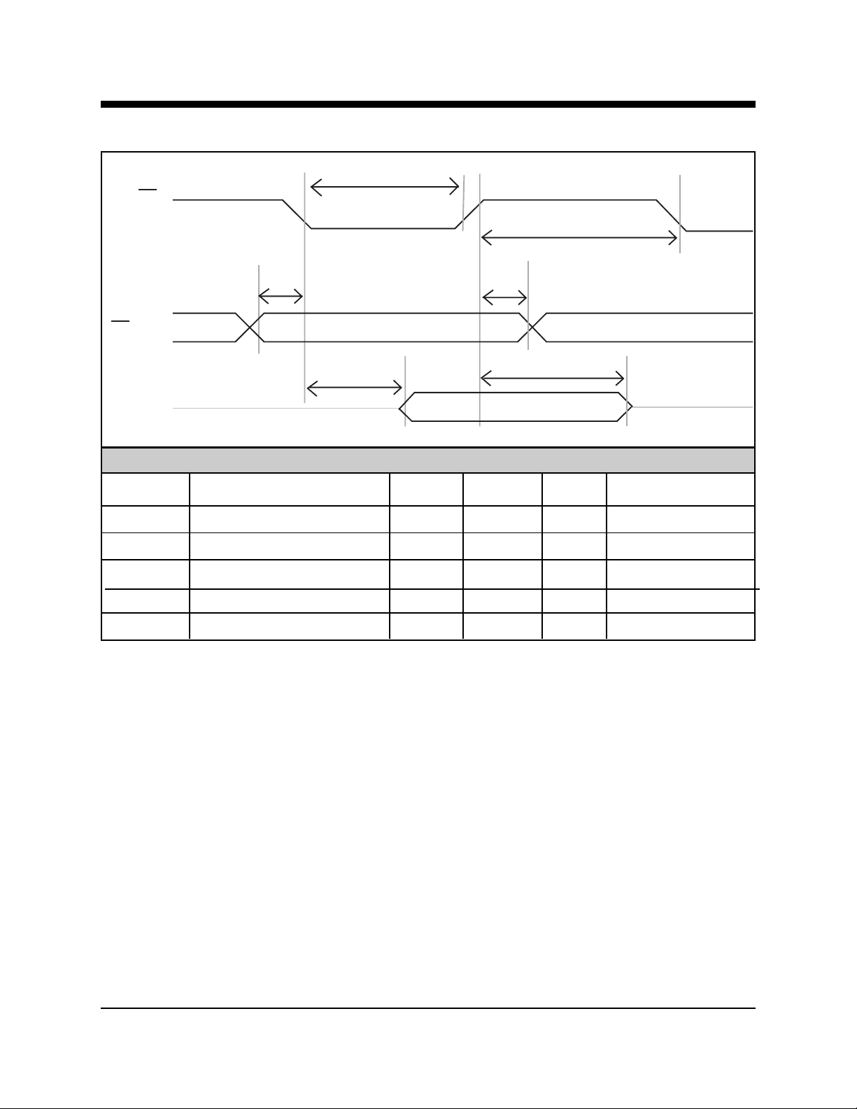
XE0068DT Write Timing
WR
T
PWL
T
PWH
T
AS
T
AH
CS, RSO
T
DHW
DATA BUS
T
DSW
Signal Definition Min Typ Max Units
TAS Address Setup Time 23 nanoseconds
TAH Address Hold Time 26 nanoseconds
TPWH Write Pulse Width High 100 nanoseconds
TPWL Write Pulse Width Low 150 nanoseconds
TDDR Data Setup Time (Write) 45 nanoseconds
TDHR Data Hold Time (Write)10This product complies with Part 68 of the FCC Rules and Regulations.
With each device shipped,there is a label which contains, among other infor mation, the FCC Registration Number and
Ringer Equivalence Number
company.
(REN) for this product. You must, upon request, give this information to your telephone
Mounting this device in the final assembly must be made in such a manner as to preserve the high voltage protection
between the TIP/RING connection and the rest of the system. Typically, this may be accomplished by maintaining a
minimum spacing .100 mils between the TIP/RING trace to the RJ-11C Jack and low voltage portion of the system. No
additional circuitry may be attached between TIP/RING and the telephone line connection unless specifically allowed in
the rules.
The REN is useful to determine the quantity of devices you may connect to the telephone line and still have all of these
devices ring when the number is called. In most, but not all areas, the sum of the RENs of all devices connected to one
line should not exceed five (5.0). To be certain of the number of devices you may connect to the line, as determined by
the REN, you should contact the local telephone company to determine the maximum REN for your calling area.
If your system causes harm to the telephone network, the telephone company may discontinue service temporarily. If
possible, they will notify you in advance. If advance notification is not practical, you will be notified as soon as possible.
Your telephone company may make changes in its facilities, equipment, operations or procedures that could affect
proper functioning of your equipment. If they do, you will be notified in advance to give you an opportunity to maintain
uninterrupted service.
XECOM (11) XE0068DT
If you experience trouble with the device, please contact XECOM an (408) 945-6640 for information on obtaining
service or repairs. The telephone company may ask you to disconnect this device from the network until the problem has
Page 12

FCC Information
This product complies with Part 68 of the FCC Rules and Regulations. With each device shipped,there is a label which
contains, among other information, the FCC Registration Number and Ringer Equivalence Number
product. You must, upon request, give this information to your telephone company.
Mounting this device in the final assembly must be made in such a manner as to preserve the high voltage protection
between the TIP/RING connection and the rest of the system. Typically, this may be accomplished by maintaining a
minimum spacing .100 mils between the TIP/RING trace to the RJ-11C Jack and low voltage portion of the system. No
additional circuitry may be attached between TIP/RING and the telephone line connection unless specifically allowed in
the rules.
The REN is useful to determine the quantity of devices you may connect to the telephone line and still have all of these
devices ring when the number is called. In most, but not all areas, the sum of the RENs of all devices connected to one
line should not exceed five (5.0). To be certain of the number of devices you may connect to the line, as determined by
the REN, you should contact the local telephone company to determine the maximum REN for your calling area.
If your system causes harm to the telephone network, the telephone company may discontinue service temporarily. If
possible, they will notify you in advance. If advance notification is not practical, you will be notified as soon as possible.
Your telephone company may make changes in its facilities, equipment, operations or procedures that could affect
proper functioning of your equipment. If they do, you will be notified in advance to give you an opportunity to maintain
uninterrupted service.
If you experience trouble with the device, please contact XECOM an (408) 945-6640 for information on obtaining
service or repairs. The telephone company may ask you to disconnect this device from the network until the problem has
been corrected or until you are sure that the device is not malfunctioning.
(REN) for this
There are no repairs that can be made by the customer to the XE0068.
The device may not be used on coin service lines provided by the telephone company (this does not apply to private coin
telephone applications which use standard telephone lines). Connection to party lines is subject to state tariffs.
FCC Registration Number DWEUSA-75283-DP-W
Ringer Equivalence 0.5B
Telephone Jack RJ11C
XECOM (12) XE0068DT
Page 13

Terms of Sale
Devices sold by XECOM are covered by the warranty provisions appearing in its Terms of Sale only. XECOM
makes no warranty, express, statutory, implied, or by description regarding the information set forth herein, or
regarding the freedom of the described devices from patent infringement. XECOM makes no warranty of
merchantability or fitness for any purposes. XECOM reserves the right to discontinue production and change
specifications and prices at any time and without notice. This product is intended for use in normal commercial
applications. Applications requiring extended temperature range, unusual environmental requirements, or high
reliability applications, such as military, medical life-support or life-sustaining equipment, are specifically not
recommended without additional processing and authorization by XECOM for such application.
Xecom assumes no responsibility for the use of any circuitry other than circuitry embodied in a Xecom
Life Support Policy
Xecom's products are not authorized for use as Critical Components in Life Support Devices or Systems.
Life Support Devices or Systems are devices or systems which, (a) are intended for surgical implant into the body,
or (b) support or sustain life, and whose failure to perform, when properly used in accordance with instructions provided in the labeling, can be reasonably expected to result in significant injury to the user.
A Critical Component is any component of a life support device or system whose failure to perform can be reasonably expected to cause failure of the life support device or system, or to affect its safety or effectiveness.
Copyright, Xecom © 1999
While Xecom, Inc. has made every effort to ensure that the information presented here is accurate, Xecom will not
be liable for any damages arising from errors or omission of fact. Xecom reserves the right to modify specifications
and/or prices without notice. Product mentioned herein are used for identification purposes only and may be trademarks and/or registered trademarks of their respective companies.
Incorporated
Xecom
374 Turquoise Street, Milpitas, CA 95035
Ph:408-945 -6640 Fax:408 -942-1346
Email: [email protected]
XECOM (13) XE0068DT
 Loading...