

Datasheet XCR3512XL-7PQ208C, XCR3512XL-7FT324C, XCR3512XL-7FT256C, XCR3512XL-12PQ208I, XCR3512XL-12PQ208C Datasheet (XILINX)
...Page 1
DS081 (v1.3) January 8, 2002 www.xilinx.com 1
Advance Product Specification 1-800-255-7778
© 2002 Xilinx, Inc. All rights reserved. All Xilinx trademarks, registered trademarks, patents, and disclaimers are as listed at http://www.xilinx.com/legal.htm.
All other trademarks and registered trademarks are the property of their respective owners. All specifications are subject to change without notice.
Features
• Lowest power 512 macrocell CPLD
• 7.5 ns pin-to-pin logic delays
• System frequencies up to 127 MHz
• 512 macrocells with 12,000 usable gates
• Available in small footprint packages
- 208-pin PQFP (180 user I/O)
- 256-ball FBGA (212 user I/O)
- 324-ball FBGA (260 user I/O)
• Optimized for 3.3V systems
- Ultra low power operation
- 5V tolerant I/O pins with 3.3V core supply
- Advanced 0.35 micron five layer metal EEPROM
process
- Fast Zero Power™ (FZP) CMOS design
technology
• Advanced syste m features
- In-system programming
- Input registers
- Predictable timing model
- Up to 23 clocks available per function block
- Excellent pin retention during design changes
- Full IEEE Standard 1149.1 boundary-scan (JTAG)
- Four global clocks
- Eight product term control term s per function block
• Fast ISP programming times
• Port Enable pin for additional I/O
• 2.7V to 3.6V supply voltage at industrial grade voltage
range
• Programmable slew rate control per output
• Security bit prevents unauthorized access
• Refer to XPLA3 family data sheet (DS012
) for
architecture description
Description
The XCR3512XL is a 3.3V, 512 macrocell CPLD targeted at
power sensitive designs that require leading edge programmable logic solutions. A total of 32 function blocks provide
12,000 usable gates. Pin-to-pin propagation delays are
7.5 ns with a maximum system frequency of 127 MHz.
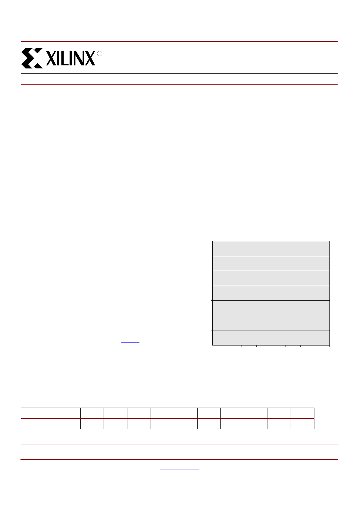
TotalCMOS Design Technique for Fast
Zero Power
Xilinx offers a TotalCMOS CPLD, both in process technology and design technique. Xilinx employs a cascade of
CMOS gates to implement its sum of products instead of
the traditional sense amp approach. This CMOS gate implementation allows Xilinx to offer CPLDs that are both high
performance and low power, breaking the paradigm that to
have low power, you must have low performance. Refer to
Figure 1 and Table 1 showing t he I
CC
vs. Frequency of our
XCR3512XL TotalCMOS CPLD (data taken with 32
resetable up/down, 16-bit counters at 3.3V, 25°C).
0
XCR3512XL: 512 Macrocell CPLD
DS081 (v1.3) January 8, 2002
014
Advance Product Specification
R
Figure 1: XCR3512XL Typical ICC vs. Frequency at
V
CC
= 3.3V, 25°C
0
20
40
60
80
100
120
140
0 20 40 60 80 100 120 140 160
DS024_01_112700
Frequency (MHz)
Typical ICC (mA)
Table 1: Typical ICC vs. Frequency at VCC = 3.3V, 25°C
Frequency (MHz) 0 1 10 20 40 60 80 100 120 140
Typical I
CC
(mA) TBD TBD TBD TBD TBD TBD TBD TBD TBD TBD
Page 2
XCR3512XL: 512 Macrocell CPLD
2 www.xilinx.com DS081 (v1.3) Janu ary 8, 2002
1-800-255-7778 Advance Product Specification
R
DC Electrical Char acteristics Over Reco mmended Operating Conditions
(1)
Symbol Parameter Test Conditions Min. Max. Unit
V
OH
(2)
Output High voltage VCC = 3.0V to 3.6V, IOH = –8 mA 2.4 - V
V
CC
= 2.7V to 3.0V, IOH = –8 mA 2.0
(3)
-V
I
OH
= –500 µA 90% V
CC
-V
V
OL
Output Low voltage IOL = 8 mA - 0.4 V
I
IL
Input leakage current VIN = GND or V
CC
–10 10 µA
I
IH
I/O High-Z leakage current VIN = GND or V
CC
–10 10 µA
I
CCSB
Standby current VCC = 3.6V - 100 µA
I
CC
Dynamic current
(4,5)
f = 1 MHz - TBD mA
f = 50 MHz - TBD mA
C
IN
Input pin capacitance
(6)
f = 1 MHz - 8 pF
C
CLK
Clock input capacitance
(6)
f = 1 MHz 5 12 pF
C
I/O
I/O pin capacitance
(6)
f = 1 MHz - 10 pF
Notes:
1. See XPLA3 f am il y data sheet (
DS012) for recommended operating conditions
2. See Figure 2 for output drive characteristics of the XPLA3 family.
3. This param eter guaranteed by design and characterization, not by testing.
4. See Table 1, Figure 1 for typical values.
5. This param eter measured with a 16-b it, resetab le up/down coun ter loaded into e very func tion bloc k, with all output s disabl ed and
unloaded. Inputs are tied to V
CC
or ground. This parameter guaranteed by design and characterization, not testing.
6. Typical values, not tested.
Page 3
XCR3512XL: 512 Macrocell CPLD
DS081 (v1.3) January 8, 2002 www.xilinx.com 3
Advance Product Specification 1-800-255-7778
R
AC Electrical Characteristics Over Recommended Operating Conditions
(1,2)
Figure 2: Typical I/V Curve for the XPLA3 Family
Symbol Parameter
-7 -10 -12
Unit Min. Max. Min. Max. Min. Max.
T
PD1
Propagation delay time (single p-term) - 9.0 - 10.8 ns
T
PD2
Propagation delay time (OR array)
(3)
- 10. 0 - 12.0 ns
T
CO
Clock to output (global synchronous pin clock) - 5.8 - 6.9 ns
T
SUF
Setup time (fast input register) 3.5 - 3.5 - ns
T
SU1
(4)
Setup time (single p-term) 5.5 - 6.7 - ns
T
SU2
Setup time (OR array) 6.5 - 7.9 - ns
T
H
(4)
Hold time 0-0-ns
T
WLH
(4)
Global Clock pulse width (High or Low) 4.0 - 5.0 - ns
Tt
PLH
(4)
P-term clock pulse width 6.0 - 7.5 - ns
T
R
(4)
Input rise time - 20 - 20 ns
T
L
(4)
Input fall time - 2 0 - 20 ns
f
SYSTEM
(4)
Maximum system frequency - 97 - 77 MHz
T
CONFIG
(4)
Configuration time
(5)
- 120 - 120 µs
T
INIT
(4)
ISP initialization time - 120 - 120 µs
T
POE
(4)
P-term OE to output enabled - 11.0 - 13.0 ns
T
POD
(4)
P-term OE to output disabled
(6)
- 11. 0 - 13.0 ns
T
PCO
(4)
P-term clock to output - 10. 3 - 12.4 ns
T
PAO
(4)
P-term set/reset to output valid - 11.0 - 13.0 ns
Notes:
1. Specifications measured with one out put switching.
2. See XPLA3 f am il y data sheet (
DS012) for recommended operating conditions.
3. See Figure 4 for derating.
4. These par am eters guaranteed by design and/or characterization, not testing.
5. Typical current draw during con figuration is 12 mA at 3.6V.
6. Output C
L
= 5 pF.
0
0
1
0
2
0
30
4
0
50
60
7
0
80
90
1
00
0.51.52.5.54.5
Volt
s
L
3.3V
)
H
3.3V
)
H
2.7V
)
A
DS012_10_04190
1
Page 4
XCR3512XL: 512 Macrocell CPLD
4 www.xilinx.com DS081 (v1.3) Janu ary 8, 2002
1-800-255-7778 Advance Product Specification
R
Internal Timing Parameters
(1,2)
Symbol Parameter
-7 -10 -12
UnitMin. Max. Min. Max. Min. Max.
Buffer Delays
T
IN
Input buffer delay - 3.3 - 4.0 ns
T
FIN
Fast input buffer delay - 3. 8 - 3.8 ns
T
GCK
Global clock buffer delay - 1.3 - 1 .5 ns
T
OUT
Output buffer delay - 3.2 - 3 .8 ns
T
EN
Output buffer enable/disable delay - 5.2 - 6 .0 ns
Internal Register and Combinatorial Delays
T
LDI
Latch transparent delay - 1.6 - 2 .0 ns
T
SUI
Register setup time 1.0 - 1.2 - ns
T
HI
Register hold time 0.5 - 0.7 - ns
T
ECSU
Register clock enable setup time 2.5 - 3.0 - ns
T
ECHO
Register clock enable hold time 4.5 - 5.5 - ns
T
COI
Register clock to output delay - 1.3 - 1 .6 ns
T
AOI
Register async. S/R to output delay - 2.0 - 2 .2 ns
T
RAI
Register async. recovery - 7.0 - 8.0 ns
T
LOGI1
Internal logic delay (single p-term) - 2.5 - 3.0 ns
T
LOGI2
Internal logic delay (PLA OR term) - 3.5 - 4 .2 ns
Feedback Delays
T
F
ZIA delay - 4.5 - 6 .0 ns
Time Adders
T
LOGI3
Fold-back NAND delay - 2.5 - 3.0 ns
T
UDA
Universal delay - 2.8 - 3.5 ns
T
SLEW
Slew rate limited delay - 5.0 - 6.0 ns
Notes:
1. These par am eters guaranteed by design and/or characterization, not testing.
2. See XPLA3 f am il y data sheet (
DS012) for timing model .
Page 5
XCR3512XL: 512 Macrocell CPLD
DS081 (v1.3) January 8, 2002 www.xilinx.com 5
Advance Product Specification 1-800-255-7778
R
Switching Characteristics
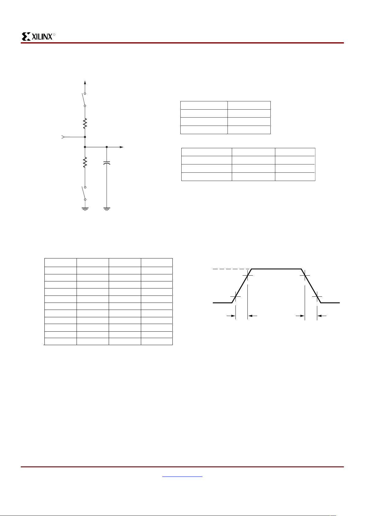
Figure 3: AC Load Circuit
DS023_03_102401
Component Values
R1 390Ω
R2 390Ω
C1 35 pF
Measurement S1 S2
T
POE
(High)
T
POE
(Low)
T
P
Open Closed
Closed Open
Closed
Closed
V
CC
V
OUT
V
IN
C1
R1
R2
S1
S2
Note: For T
POD
, C1 = 5 pF. Delay measured at
output level of V
OL
+ 300 mV, VOH – 300 mV.
Figure 4: Derating Curve for T
PD2
6.3
6.4
6.5
6.6
6.7
6.8
6.9
7.0
7.1
7.2
7.3
7.4
7.5
124816
DS024_04_11800
Number of Adjacent Outputs Switching
(ns)
Figure 5: Voltage Waveform
90%
10%
1.5 ns 1.5 ns
DS017_05_042800
+3.0V
0V
Measurements:
All circuit delays are measured at the +1.5V level of
inputs and outputs, unless otherwise specified.
T
R
T
L
Page 6

XCR3512XL: 512 Macrocell CPLD
6 www.xilinx.com DS081 (v1.3) Janu ary 8, 2002
1-800-255-7778 Advance Product Specification
R
Pin Des cr ip t io ns
Table 2: XCR3512XL User I/O Pins
PQ208 FT256 FG324
Total User I/O Pins 180 212 260
Table 3: XCR3512XL I/O Pins
Function
Block Macrocell PQ208 FT256 FG324
1 1 208 C14 C21
12-D13C20
1 3 207 - B22
1 4 206 A15 B21
1 5--1 6--1 7--1 8--1 9--110--111--112--113--A22
1 14 205 B15 A21
115-B14B20
1 16 204 C13 C19
211E12D20
22--C22
232A16D21
24-C15D22
2 5--2 6--2 7--2 8--2 9--210--211--212--2133B16E20
2144D14F19
215--E21
2166D15E22
3 1 203 A14 B19
32-E11A20
3 3 202 - C18
3 4 201 A13 B18
35--36--37--38--39--310--311--312--313-D12A19
314--D17
3 15 199 B13 A18
3 16 198 C12 C17
417E13F20
42--F21
438C16F22
449F12G19
45--46--47--48--49--410--411--412--413--G20
41410D16G21
415-E14G22
41611E15H20
Table 3: XCR3512XL I/O Pins (Continued)
Function
Block Macrocell PQ208 FT256 FG324
Page 7

XCR3512XL: 512 Macrocell CPLD
DS081 (v1.3) January 8, 2002 www.xilinx.com 7
Advance Product Specification 1-800-255-7778
R
5 1 197 A12 B17
52--A17
5 3 196 D11 D16
54--C16
5 5--5 6--5 7--5 8--5 9--510--511--512--5 13 195 A11 B16
514-E10A16
5 15 194 B12 C15
5 16 193 C11 B15
6 1 12 F13 H21
62--H22
6 3 13 E16 J19
64--J20
6 5--6 6--6 7--6 8--6 9--610--611--612--61315F15J21
61416G12J22
615-F14K19
61617G15K20
7 1 192 B11 A15
72-D10D14
7 3 190 A10 C14
Table 3: XCR3512XL I/O Pins (Continued)
Function
Block Macrocell PQ208 FT256 FG324
7 4 189
(1)
C10
(1)
B14
(1)
75--76--77--78--79--710--711--712--7 13 188 - A14
714--D13
715-A9C13
7 16 187 D9 B13
8 1 18 G13 K21
82--K22
8 3 19 F16 L19
8 4 - - L20
85--86--87--88--89--810--811--812--8 13 20 G14 L21
8 14 21 G16 L22
81522H13M21
81624H12M20
9 1 51 P16 AA21
9 2 - N14 AB22
9349R16AA22
94--Y20
95--96---
Table 3: XCR3512XL I/O Pins (Continued)
Function
Block Macrocell PQ208 FT256 FG324
Page 8

XCR3512XL: 512 Macrocell CPLD
8 www.xilinx.com DS081 (v1.3) Janu ary 8, 2002
1-800-255-7778 Advance Product Specification
R
9 7--9 8--9 9--910--911--912--91348M13Y21
91447P15W20
9 15 46 L12 W21
91645N16Y22
10 1 52 N13 AB21
10 2 53 R15 Y19
10 3 54 M12 AA20
10 4 - - AB20
105 --106 --107 --108 --109 --1010--1011--1012--10 13 55 T16 Y18
10 14 56 P14 AA19
10 15 - T15 AB19
10 16 57 P13 W17
11 1 44 M14 W 22
11 2 43 M16 V20
11 3 42 L13 V 21
11 4 - N15 U19
115 --116 --117 --118 --119 ---
Table 3: XCR3512XL I/O Pins (Continued)
Function
Block Macrocell PQ208 FT256 FG324
11 10 - - 11 11 - - 11 12 - - 11 13 - - V22
11 14 40 M15 U20
11 15 39 L16 U21
11 16 38 K12 U22
12 1 58 R 14 Y17
12 2 - N12 AA18
12 3 59 T14 AB18
12 4 - - AA17
12 5 - - 12 6 - - 12 7 - - 12 8 - - 12 9 - - 12 10 - - 12 11 - - 12 12 - - 12 13 60 M11 AB17
12 14 - R13 W16
12 15 61 P12 Y16
12 16 62 T13 AA16
13 1 37 L15 T19
13 2 - - T20
13 3 36 K13 T21
13 4 35 K16 T22
13 5 - - 13 6 - - 13 7 - - 13 8 - - 13 9 - - 13 10 - - 13 11 - - 13 12 - - -
Table 3: XCR3512XL I/O Pins (Continued)
Function
Block Macrocell PQ208 FT256 FG324
Page 9

XCR3512XL: 512 Macrocell CPLD
DS081 (v1.3) January 8, 2002 www.xilinx.com 9
Advance Product Specification 1-800-255-7778
R
13 13 - K14 R20
13 14 34 K15 R21
13 15 33 L14 R22
13 16 31 J16 P19
14 1 64 N11 AB16
14 2 - R12 Y15
14 3 65 T12 AA15
14 4 66 R11 AB15
145 --146 --147 --148 --149 --1410--1411--1412--14 13 67 M10 W14
14 14 68 P11 Y14
14 15 - - AA14
14 16 69 N10 AB14
15 1 30
(1)
J13
(1)
P20
(1)
15 2 29 J15 P21
15 3 28 J14 P22
15 4 - - N19
155 --156 --157 --158 --159 --1510--1511--1512--15 13 27 H16 N21
15 14 - - N22
15 15 26 H14 M22
Table 3: XCR3512XL I/O Pins (Continued)
Function
Block Macrocell PQ208 FT256 FG324
15 16 25 H15 M19
16 1 70 T11 W13
16 2 71 R 10 Y13
16 3 73 P10 AA13
16 4 - T 10 AB13
16 5 - - 16 6 - - 16 7 - - 16 8 - - 16 9 - - 16 10 - - 16 11 - - 16 12 - - 16 13 - - W12
16 14 76 N9 AA12
16 15 77 R9 AB12
16 16 78 P9 Y11
17 1 157 B1 C3
17 2 - B2 A2
17 3 158 C3 B3
17 4 - - C4
17 5 - - 17 6 - - 17 7 - - 17 8 - - 17 9 - - 17 10 - - 17 11 - - 17 12 - - 17 13 159 D4 B4
17 14 - A2 C5
17 15 160 A1 B5
17 16 161 B3 A3
18 1 156 C1 D3
18 2 155 D3 B2
Table 3: XCR3512XL I/O Pins (Continued)
Function
Block Macrocell PQ208 FT256 FG324
Page 10

XCR3512XL: 512 Macrocell CPLD
10 www.xilinx.com DS081 (v1.3) January 8, 2002
1-800-255-7778 Advance Product Specification
R
18 3 154 C2 B1
18 4 153 F5 C2
185 --186 --187 --188 --189 --1810--1811--1812--18 13 - - C1
18 14 151 D1 E3
18 15 - - D2
18 16 150 E4 D1
19 1 162 C4 A4
19 2 - - D6
19 3 163 A3 A5
19 4 - D5 C6
195 --196 --197 --198 --199 --1910--1911--1912--19 13 164 B4 B6
19 14 - E6 A6
19 15 166 A4 D7
19 16 167 C5 C7
20 1 149 D2 F4
20 2 148 E3 F3
20 3 - - E2
20 4 147 E1 E1
205 ---
Table 3: XCR3512XL I/O Pins (Continued)
Function
Block Macrocell PQ208 FT256 FG324
20 6 - - 20 7 - - 20 8 - - 20 9 - - 20 10 - - 20 11 - - 20 12 - - 20 13 - - F2
20 14 146 F4 F1
20 15 145 F1 G4
20 16 144 G5 G3
21 1 168 B5 B7
21 2 - D6 A7
21 3 169 A5 C8
21 4 - - B8
21 5 - - 21 6 - - 21 7 - - 21 8 - - 21 9 - - 21 10 - - 21 11 - - 21 12 - - 21 13 170 C6 A8
21 14 171 B6 D9
21 15 - E7 C9
21 16 172 A6 B9
22 1 142 E2 G2
22 2 141 F3 G1
22 3 - - H3
22 4 140 F2 H2
22 5 - - 22 6 - - 22 7 - - 22 8 - - -
Table 3: XCR3512XL I/O Pins (Continued)
Function
Block Macrocell PQ208 FT256 FG324
Page 11

XCR3512XL: 512 Macrocell CPLD
DS081 (v1.3) January 8, 2002 www.xilinx.com 11
Advance Product Specification 1-800-255-7778
R
229 --2210--2211--2212--22 13 - - H1
22 14 139 G4 J4
22 15 - G1 J3
22 16 138 G3 J2
23 1 173 D7 A9
23 2 - B7 D10
23 3 175 C7 C10
23 4 - C8 B10
235 --236 --237 --238 --239 --2310--2311--2312--23 13 - - A10
23 14 17 6
(1)
A7
(1)
D11
(1)
23 15 177 D8 C11
23 16 178 B8 B11
24 1 137 H1 J1
24 2 136 H4 K4
24 3 135 G2 K3
24 4 - H3 K2
245 --246 --247 --248 --249 --2410--2411---
Table 3: XCR3512XL I/O Pins (Continued)
Function
Block Macrocell PQ208 FT256 FG324
24 12 - - 24 13 133 J1 K1
24 14 - - L1
24 15 - - L4
24 16 132 J3 L 3
25 1 105 P2 AA1
25 2 106 P3 Y3
25 3 - - Y2
25 4 108 T1 W3
25 5 - - 25 6 - - 25 7 - - 25 8 - - 25 9 - - 25 10 - - 25 11 - - 25 12 - - 25 13 - - Y1
25 14 109 N3 W2
25 15 110 R1 W1
25 16 111 M4 V3
26 1 104 M5 AB1
26 2 - N4 AA2
26 3 103 R2 AB2
26 4 - T2 AA3
26 5 - - 26 6 - - 26 7 - - 26 8 - - 26 9 - - 26 10 - - 26 11 - - 26 12 - - 26 13 102 P4 Y4
26 14 - - AB3
Table 3: XCR3512XL I/O Pins (Continued)
Function
Block Macrocell PQ208 FT256 FG324
Page 12

XCR3512XL: 512 Macrocell CPLD
12 www.xilinx.com DS081 (v1.3) January 8, 2002
1-800-255-7778 Advance Product Specification
R
26 15 101 R3 AA4
26 16 100 N5 Y5
27 1 112 P1 U4
27 2 - - V2
27 3 113 L5 V1
27 4 114 N2 U3
275 --276 --277 --278 --279 --2710--2711--2712--27 13 - - U2
27 14 115 M3 U1
27 15 117 L4 T3
27 16 118 M2 T2
28 1 99 T 3 AA5
28 2 98 M6 AB4
28 3 - R4 W6
28 4 97 P5 AB5
285 --286 --287 --288 --289 --2810--2811--2812--28 13 - - Y6
28 14 96 T4 AA6
28 15 95 N6 AB6
28 16 93 R5 W7
29 1 119 L2 T1
Table 3: XCR3512XL I/O Pins (Continued)
Function
Block Macrocell PQ208 FT256 FG324
29 2 - - R3
29 3 120 M1 R2
29 4 121 K5 R1
29 5 - - 29 6 - - 29 7 - - 29 8 - - 29 9 - - 29 10 - - 29 11 - - 29 12 - - 29 13 122 L3 P4
29 14 123 K4 P3
29 15 - - P2
29 16 124 L1 P1
30 1 92 T6 Y7
30 2 - T5 AA7
30 3 91 M7 AB7
30 4 - - Y8
30 5 - - 30 6 - - 30 7 - - 30 8 - - 30 9 - - 30 10 - - 30 11 - - 30 12 - - 30 13 90 R6 AA8
30 14 89 N7 AB8
30 15 88 T7 W9
30 16 87 P6 Y9
31 1 126 K2 N4
31 2 - K 3 N3
31 3 127
(1)
K1
(1)
N2
(1)
31 4 128 J4 N1
Table 3: XCR3512XL I/O Pins (Continued)
Function
Block Macrocell PQ208 FT256 FG324
Page 13

XCR3512XL: 512 Macrocell CPLD
DS081 (v1.3) January 8, 2002 www.xilinx.com 13
Advance Product Specification 1-800-255-7778
R
315 --316 --317 --318 --319 --3110--3111--3112--31 13 - - M4
31 14 129 J2 M 3
31 15 130 J5 M 2
31 16 131 H2 L2
32 1 86 R7 AA9
32 2 - P7 AB9
32 3 84 T 8 W 10
32 4 - N8 Y10
325 --326 --327 --328 --329 --3210--3211--3212--32 13 - - AA10
32 14 81 R8 AB11
32 15 80 P8 W 11
32 16 79 T9 AA11
Notes:
1. JTAG pins.
Table 3: XCR3512XL I/O Pins (Continued)
Function
Block Macrocell PQ208 FT256 FG324
Table 4: XCR3512XL Global, JT A G, P ort Enable, Power ,
and No Co nnect Pins
Pin Type PQ208 FT256 F G324
IN0 / CLK0 181 B9 C12
IN1 / CLK1 182 A8 B12
IN2 / CLK2 183 C9 D12
IN3 / CLK3 184 B10 A12
TCK 30 J13 P20
TDI 176 A7 D11
TDO 189 C10 B14
TMS 127 K1 N2
PORT_EN 116
(1)
N1
(1)
T4
(1)
Vcc 5, 23, 41, 63,
74, 83, 85,
107, 125,
143, 165,
179, 186,
191
E8, E9, F7,
F8, F9, F10,
G6, G1 1, H5,
H6, H11, J6,
J11, J12, K6,
K11, L7, L8,
L9, L10, M8,
M9
A11, A13,
D8, D15, H4,
H19, J10,
J11, J12,
J13, K9,
K14, L9,
L14, M1, M9,
M14, N9,
N14, N20,
P10, P11,
P12, P13,
R4, R19,
W8, W15,
Y12, AB10
GND 14, 32, 50,
72, 75, 82,
94, 134, 152,
174, 180,
185, 200
E5, F6, F11,
G7, G8, G9,
G10, H7, H8,
H9, H10, J7,
J8, J9, J10,
K7, K8, K9,
K10, L6, L11
D4, D5, D18,
D19, E4,
E19, J9, J14,
K10, K11,
K12, K13,
L10, L11,
L12, L13,
M10, M11 ,
M12, M13 ,
N10, N11,
N12, N13,
P9, P14, V4,
V19, W4,
W5, W18,
W19
No
Connects
--A1
Notes:
1. Po rt Enable is br ought High t o enabl e JTAG pins when JTAG
pins are used as I/O . See f amily data she et (
DS012) f or full
explanation.
Page 14

XCR3512XL: 512 Macrocell CPLD
14 www.xilinx.com DS081 (v1.3) January 8, 2002
1-800-255-7778 Advance Product Specification
R
Ordering Information
Revision History
The following table shows the revision history for this document
Component Compatibility
Pins 208 256 324
Type Plastic PQFP Plastic FBGA Plastic FBGA
Code PQ208 FT256 F G324
XCR3512XL
-7 C C C
-10 C, I C, I C, I
-12 C, I C, I C, I
Date Version Revision
04/11 /01 1.0 Initia l X ilin x re lea s e.
04/19/01 1.1 Updated Typical I/V curve, Figure 2: added voltage levels.
09/04/01 1.2 Updated AC Electrical: added T
INIT
spec.; Internal Timing Parameters; added -12 industrial
temperature.
01/08/02 1.3 Updated T
INIT
spec and T
CONFIG
spec. Added single p-term setup time (T
SU1
) to AC Table,
renamed T
SU
to T
SU2
for setup time through the OR array. Updat ed THI spec to correct a
typo. Updated AC Load Circuit diagram to more closely resemble true test conditions, added
note for T
POD
delay measurement.
XCR3512XL -10 PQ 208 C
Example:
Temperature Range
Number of Pins
Package Type
Device Type
Speed Grade
Device Ordering Options
Speed Package Temperature
-12 12 ns pin-to-pin dela y PQ208 208-pin Plastic Quad Fla t Package C = Commercial T
A
= 0°C to +70°C
V
CC
= 3.0V to 3.6V
-10 10 ns pin-to-pin delay FT256 256-ball Fineline BGA Package I = Industrial T
A
= –40°C to +85°C
V
CC
= 2.7V to 3.6V
-7 7.5 ns pin-to-pin delay FG324 324-ball Finelin e BGA P ackage
 Loading...