

Datasheet XC95288XV-7FG256C, XC95288XV-7CS280C, XC95288XV-5TQ144C, XC95288XV-5PQ208C, XC95288XV-5FG256C Datasheet (XILINX)
...Page 1
DS050 (v2.2) August 27, 2001 www.xilinx.com 1
Advance Product Specification 1-800-255-7778
© 2001 Xilinx, Inc. All rights reserved. All Xilinx trademarks, registered trademarks, patents, and disclaimers are as listed at http://www.xilinx.com/legal.htm.
All other trademarks and registered trademarks are the property of their respective owners. All specifications are subject to change without notice.
Features
• 288 macrocells with 6,400 usable gates
• Available in small footprint packages
- 144-pin TQFP (117 user I/O pins)
- 208-pin PQFP (168 user I/O pins)
- 280-pin CSP (192 user I/O pins)
- 256-pin FBGA (192 user I/O pins)
• Optimized for high-perfo rmance 2.5V systems
- Low power operation
- Multi-voltage operation
• Advanced system features
- In-system programmable
- Four separate output banks
- Superior pin-locking and routability with
FastCONNECT II™ switch matrix
- Extra wide 54-input Function Blocks
- Up to 90 product-terms per macrocell with
individual product-term allocation
- Local clock inversion with three global and one
product-term clocks
- Individual output enable per output pin
- Input hysteresis on all user and boundary-scan pin
inputs
- Bus-hold ciruitry on all user pin inputs
- Full IEEE Standard 1149.1 boundary-scan (JTAG)
• Fast concurrent programming
• Slew rate control on individual outputs
• Enhanced data security features
• Excellent quality and reliability
- Endurance exceeding 10,000 program/erase
cycles
- 20 year data retention
- ESD protection exceeding 2,000V
Description
The XC95288XV is a 2.5V CPLD targeted for high-performance, low-voltage applications in leading-edge communications and computing systems. It is comprised of 16
54V18 Function Blocks, providing 6,400 usable gates with
propagation delays of 5 ns.
Power Estimation
Power dissipation in CPLDs can vary substantially depending on the system frequency, design application and output
loading. To help reduce power dissipation, each macrocell
in a XC9500XV device may be configured for low-power
mode (from the default high-performance mode). In ad dition, unused product-terms and macrocells are automatically deactivated by the software to further conserve power.
For a general estimate of I
CC
, the following equation may be
used:
I
CC
(mA) =
MC
HP
(0.36) + MCLP(0.23) + MC(0.005 mA/MHz) f
Where:
MC
HP
= Macrocells in high-performance (default) mode
MC
LP
= Macrocells in low-power mode
MC = Total number of macrocells used
f = Clock frequency (MHz)
This calculation is based on typical operating conditions
using a pattern of 16-bit up/down counters in each Function
Block with no output loading. The actual I
CC
value varies
with the design application and should be verified during
normal system operation.
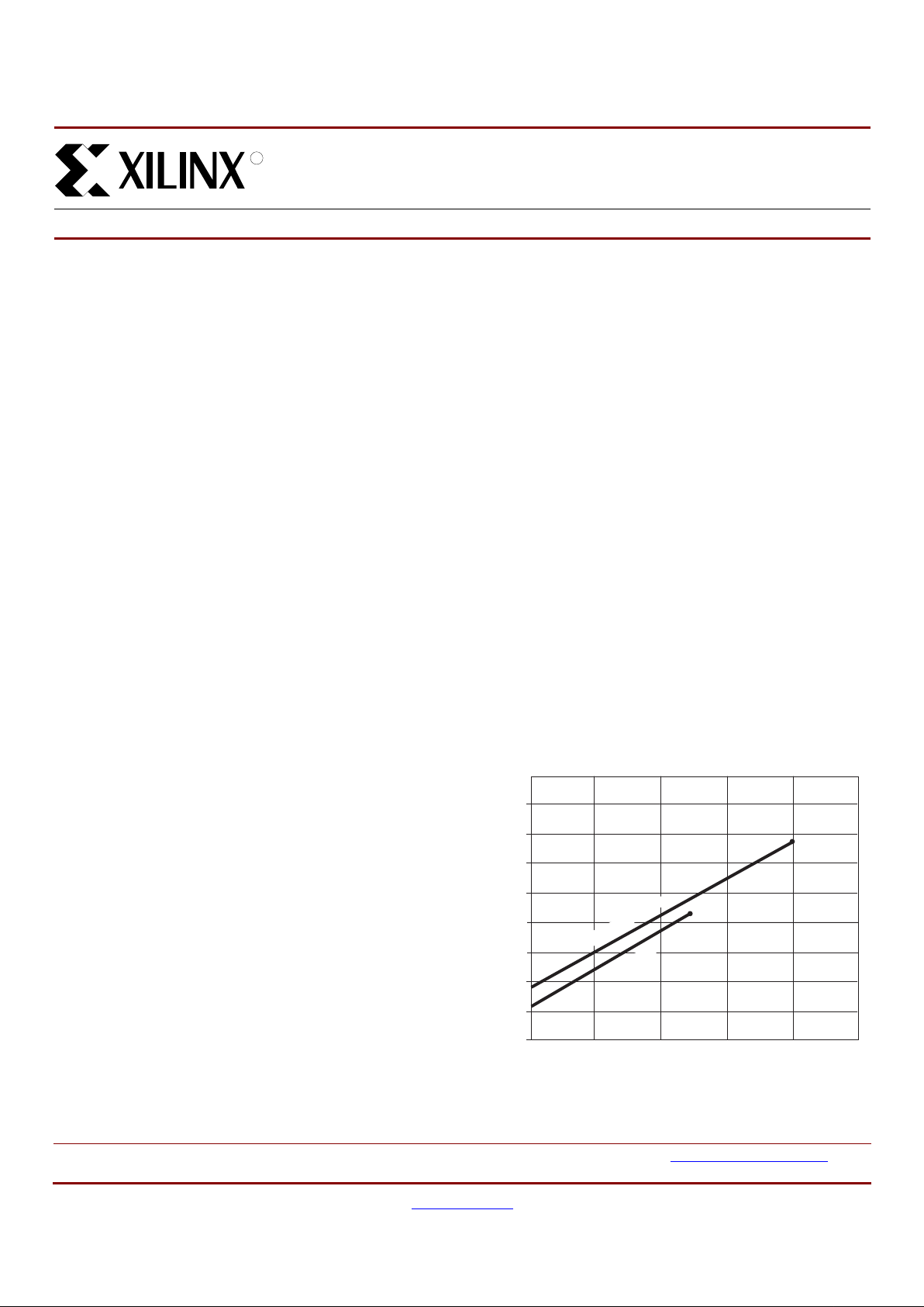
Figure 1 shows the above estimation in a graphical form.
0
XC95288XV High-Performance
CPLD
DS050 (v2.2) August 27, 2001
05
Advance Product Specification
R
Figure 1: Typical I
CC
vs. Frequency for XC95288XV
Clock Frequency (MHz)
Typical I
CC
(mA)
100 200 250
DS050_01_012501
200
250
300
350
400
450
50
50 150
150
100
0
120 MHz
H
i
gh P
e
r
form
a
nce
200 MHz
Low Powe
r
Page 2
XC95288XV High-Performance CPLD
2 www.xilinx.com DS050 (v2.2) Augus t 27, 2001
1-800-255-7778 Advance Product Specification
R
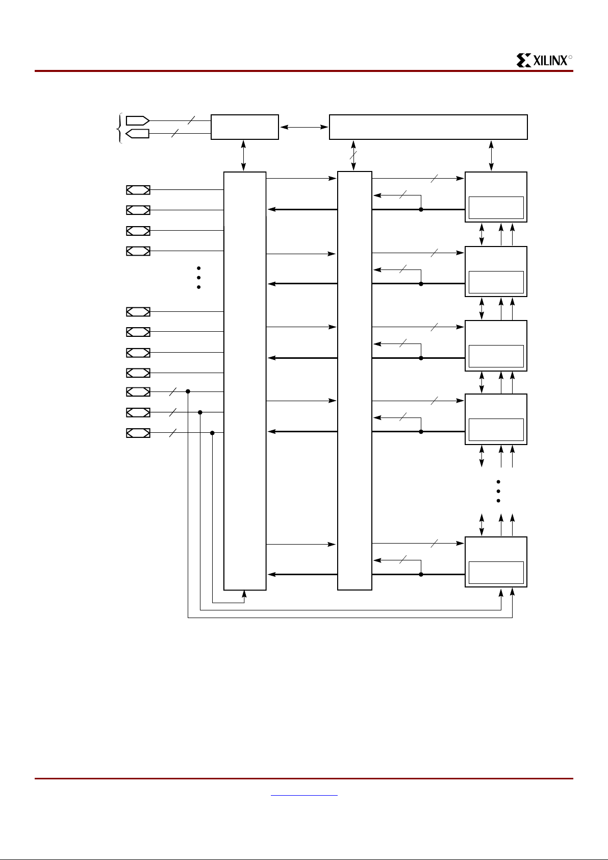
Figure 2: XC9528 8X V Architecture
(Function Block outputs (indicated by the bold line) drive the I/O Blocks directly.)
In-System Programming Controller
JTAG
Controller
I/O
Blocks
Function
Block 1
Macrocells
1 to 18
Macrocells
1 to 18
JTAG Port
3
54
I/O/GTS
I/O/GSR
I/O/GCK
I/O
I/O
I/O
I/O
4
1
I/O
I/O
I/O
I/O
3
DS055_02_101300
1
Function
Block 2
54
18
18
Function
Block 3
Macrocells
1 to 18
Macrocells
1 to 18
54
Function
Block 16
54
18
18
Function
Block 4
Macrocells
1 to 18
54
18
FastCONNECT II Switch Matrix
Page 3
XC95288XV High-Performance CPLD
DS050 (v2.2) August 27, 2001 www.xilinx.com 3
Advance Product Specification 1-800-255-7778
R
Absolute Maximum Ratings
Recommended Operation Conditions
Quality and Reliability Characteristics
Symbol Description Value Units
V
CC
Supply voltage relative to GND –0.5 to 2.7 V
V
CCIO
Supply voltage for output drivers –0.5 to 3.6 V
V
IN
Input voltage relative to GND
(1)
–0.5 to 3.6 V
V
TS
Voltage applied to 3-state output
(1)
–0.5 to 3.6 V
T
STG
Storage temperature (ambient) –65 to +150
o
C
T
SOL
Maximum soldering temperature (10s @ 1/16 in. = 1.5 mm) +260
o
C
T
J
Junction temperature +150
o
C
Notes:
1. Maximum DC unders hoot bel ow GND must be l imit ed to ei ther 0. 5V or 10 mA , whi chever is easi er to a chie v e . During tr a nsitions , the
device pins may undershoot to –2.0V or overshoot to +3.6V, provided this over- or undershoot lasts less than 10 ns and with the
forcing current being limited to 200 mA.
2. Stresses beyond those listed under Absolute Maximum Ratings may cause permanent damage to the device. These are stress
ratings only, and functional operation of the device at these or any other conditions bey ond those listed under Operating Conditions
is not implied. Exposure to Absolute Maximum Ratings condition s for ext ended periods of time may affect device reliability.
Symbol Parameter Min Max Units
V
CCINT
Supply voltage for internal logic
and input buffers
Commercial TA = 0oC to +70oC2.372.62 V
Industrial T
A
= –40oC to +85oC2.372.62
V
CCIO
Supply voltage for output drivers for 3.3V operation 3.13 3.46 V
Supply voltage for output drivers for 2.5V operation 2.37 2.62 V
Supply voltage for output drivers for 1.8V operation 1.71 1.89 V
V
IL
Low-level input volt ag e 0 0.8 V
V
IH
High-level input voltage 1.7 3.6 V
V
O
Output voltage 0 V
CCIO
V
Symbol Parameter Min Max Units
T
DR
Data retention 20 - Years
N
PE
Program/Erase cycles (endurance) 10,000 - Cycles
V
ESD
Electrostatic Discharge (ESD) 2,000 - Volts
Page 4
XC95288XV High-Performance CPLD
4 www.xilinx.com DS050 (v2.2) Augus t 27, 2001
1-800-255-7778 Advance Product Specification
R
DC Characteristics Over Recommended Operating Conditions
AC Characteristics
Symbol Parameter Test Conditions Min Max Units
V
OH
Output high voltage for 3.3V outputs IOH = –4.0 mA 2.4 - V
Output high voltage for 2.5V outputs I
OH
= –1.0 mA 2.0 - V
Output high voltage for 1.8V outputs I
OH
= –100 µA90%
V
CCIO
-V
V
OL
Output low voltage for 3.3V outputs IOL = 8.0 mA - 0.4 V
Output low voltage for 2.5V outputs I
OL
= 1.0 mA - 0.4 V
Output low voltage for 1.8V outputs I
OL
= 100 µA-0.4V
I
IL
Input leakagelow current VCC = 2.62V
V
CCIO
= 3.6V
V
IN
= GND or 3.6V
-10µA
I
IH
Input leakage high current VCC = 2.62V
V
CCIO
= 3.6V
V
IN
= GND or 3.6V
-10µA
C
IN
I/O capacitance VIN = GND
f = 1.0 MHz
-10pF
I
CC
Operating Supply Current
(low power mode, active)
VI = GND, No load
f = 1.0 MHz
59 mA
Symbol Parameter
XC95288XV-5 XC95288XV-7 XC95288XV-10
UnitsMin Max Min Max Min Max
T
PD
I/O to output valid - 5.0 - 7.5 - 10 ns
T
SU
I/O setup time before GCK 3.5 - 4.8 - 6.5 - ns
T
H
I/O hold time after GCK 0 - 0 - 0 - ns
T
CO
GCK to output valid - 3.5 - 4.5 - 5.8 ns
f
SYSTEM
Multiple FB internal operating
frequency
- 222.2 - 125.0 - 100.0 MHz
T
PSU
I/O setup time before p-term clock
input
1.0 - 1.6 - 2.1 - ns
T
PH
I/O hold time after p-term clock input 2.5 - 3.2 - 4.4 - ns
T
PCO
P-term clock output valid - 6.0 - 7.7 - 10.2 ns
T
OE
GTS to output valid - 4.0 - 5 .0 - 7.0 ns
T
OD
GTS to output disable - 4.0 - 5 .0 - 7.0 ns
T
POE
Product term OE to output enabled - 7.0 - 9.5 - 11.0 ns
T
POD
Product term OE to output disabled - 7.0 - 9.5 - 11.0 ns
T
AO
GSR to output valid - 10.0 - 12.0 - 14.5 ns
T
PAO
P-term S/R to output valid - 10.7 - 12. 6 - 15.3 ns
T
WLH
GCK pulse width (High or Low) 2.2 - 4.0 - 5.0 - ns
T
PLH
P-term clock pulse width (High or Low) 5.0 - 6.5 - 7.0 - ns
Advance Information Preliminary Information
Notes:
1.
Please c on t ac t X ilin x for up-to-date infor mation on ad vanc e specificat ions.
Page 5

XC95288XV High-Performance CPLD
DS050 (v2.2) August 27, 2001 www.xilinx.com 5
Advance Product Specification 1-800-255-7778
R
Internal Timing Parameters
Figure 3: AC Load Circuit
Symbol Parameter
XC95288XV-5 XC95288XV-7 XC95288XV-10
UnitsMin Max Min Max Min Max
Buffer Delays
T
IN
Input buffer delay - 2.0 - 2.3 - 3.5 ns
T
GCK
GCK buffe r delay - 1.2 - 1.5 - 1.8 ns
T
GSR
GSR buffer delay - 2.0 - 3.1 - 4.5 ns
T
GTS
GTS buffer delay - 4.0 - 5.0 - 7.0 ns
T
OUT
Output buffer delay - 2.1 - 2.5 - 3.0 ns
T
EN
Output buffer enable/disable delay - 0 - 0 - 0 ns
Product Term Contr ol Delays
T
PTCK
Product term clock delay - 1.7 - 2.4 - 2.7 ns
T
PTSR
Product term set/reset delay - 0.7 - 1.4 - 1.8 ns
T
PTTS
Product term 3-state delay - 5.0 - 7.2 - 7.5 ns
Internal Register and Combinatorial Delays
T
PDI
Combinatorial logic propagation delay - 0.2 - 1.3 - 1.7 ns
T
SUI
Register setup time 2.0 - 2.6 - 3.0 - ns
T
HI
Register hold time 1.5 - 2. 2 - 3.5 - ns
T
ECSU
Register clock enable setup time 2.0 - 2.6 - 3.0 - ns
T
ECHO
Register clock enable hold time 1.5 - 2.2 - 3.5 - ns
T
COI
Register clock to output valid time - 0.2 - 0.5 - 1.0 ns
T
AOI
Register async. S/R to output delay - 5.9 - 6.4 - 7.0 ns
T
RAI
Register async. S/R recover before clock 5.0 7.5 10.0 - ns
T
LOGI
Internal logic delay - 0.7 - 1.4 - 1.8 ns
T
LOGILP
Internal low power logic delay - 5.7 - 6.4 - 7.3 ns
Feedback Delays
T
F
FastCONNECT II feedback delay - 1.6 - 3.5 - 4.2 ns
Time Adders
T
PTA
Incremental product term allocator delay - 0.7 - 0.8 - 1.0 ns
T
PTA2
Adjacent macrocell p-term allocator delay - 0.3 - 0.3 - 0.4 ns
T
SLEW
Slew-rate limited delay - 3.0 - 4.0 - 4.5 ns
Advance Information Preliminary Information
Notes:
1.
Please contact Xilinx for up-to-date information on advance specifications.
R
1
V
TEST
C
L
R
2
Device Output
Output Type V
TEST
3.3V
2.5V
R
1
320Ω
250Ω
R
2
360Ω
660Ω
C
L
35 pF
35 pF
DS052_03_041200
V
CCIO
3.3V
2.5V
1.8V
Page 6

XC95288XV High-Performance CPLD
6 www.xilinx.com DS050 (v2.2) Augus t 27, 2001
1-800-255-7778 Advance Product Specification
R
XC95288XV I/O Pins
Function
Block
Macro-
cell
TQ144 PQ208 FG256 CS280
BScan
Order Bank
Function
Block
Macro-
cell
TQ144 PQ208 FG256 CS280
BScan
Order Bank
1 1 - - - - 861 - 3 1 - ---7531 2 - 28 H1 K2 858 1 3 2 28 38 L2 N2 750 1
1 3 - 29 H5 K3 855 1 3 3 - 3 9 L5 P1 747 1
1 4 - - - - 852 - 3 4 - - - -7441 5 20 30 J1 K4 849 1 3 5 - 40 M1 P2 741 1
1 6 21 31 J5 L1 846 1 3 6 - 41 L4 P3 738 1
1 7 - - - - 843 - 3 7 - - - -7351 8 22 32 J2 L2 840 1 3 8 - 43 N1 P4 732 1
1 9 - - J3 L3 837 1 3 9 - -L3R17291
1 10 23 33 K1 L4 834 1 3 10 30
(1)
44
(1)
M2
(1)
R3
(1)
726 1
1 11 - - J4 M1 831 1 3 11 - -M4R27231
1 12 24 34 K2 M2 828 1 3 12 31 45 P1 R4 720 1
1 13 - - - - 825 - 3 13 - - - -7171 14 25 35 K5 M3 822 1 3 14 32
(1)
46
(1)
M3
(1)
T1
(1)
714 1
1 15 26 36 L1 M4 819 1 3 15 33 47 N2 T2 711 1
1 16 - - - - 816 - 3 16 - ---7081 17 27 37 K3 N1 813 1 3 17 - 48 N4 T3 705 1
1 18 - - - - 810 -
318----7022 1 - - - - 807 - 4 1 - ---6992 2 9 15 D1 G3 804 2 4 2 2
(1)
3
(1)
D3
(1)
C2
(1)
696 2
2 3 10 16 G4 G2 801 2 4 3 - 4D2B16932
2 4 - - - - 798 - 4 4 - - - -6902 5 11 17 E1 G1 795 2 4 5 3
(1)
5
(1)
E3
(1)
C1
(1)
687 2
2 6 12 18 G3 G4 792 2 4 6 4 6C2D46842
2 7 - - - - 789 - 4 7 - - - -6812 8 13 19 G2 H1 786 2 4 8 5
(1)
7
(1)
D4
(1)
D3
(1)
678 2
2 9 - - F5 H3 783 2 4 9 - -B1D26752
2 10 14 20 F1 H2 780 2 4 10 - 8E4D16722
2 11 - - G5 H4 777 2 4 11 - -C1E36692
2 12 15 21 H2 J1 774 2 4 12 6
(1)
9
(1)
E5
(1)
E2
(1)
666 2
2 13 - - - - 771 - 4 13 - - - -6632 14 16 22 H4 J2 768 2 4 14 7 10 E2 E4 660 2
2 15 17 23 G1 J3 765 2 4 15 - 12 F2 F3 657 2
2 16 - - - - 762 - 4 16 - - - -6542 17 19 25 H3 J4 759 2 4 17 - 14 E6 F4 651 2
218
- - - - 756 - 418- - - -648-
Notes:
1. Global contro l pi n
Page 7

XC95288XV High-Performance CPLD
DS050 (v2.2) August 27, 2001 www.xilinx.com 7
Advance Product Specification 1-800-255-7778
R
XC95288XV I/O Pins (continued)
Function
Block
Macro-
cell
TQ144 PQ208 FG256 CS280
BScan
Order Bank
Function
Block
Macro-
cell
TQ144 PQ208 FG256 CS280
BScan
Order Bank
5 1 - - - - 645 - 7 1 - - - - 537 5 2 34 49 R1 U1 642 1 7 2 - 62 R3 W5 534 1
5 3 - 5 0 N3 V1 639 1 7 3 45 63 M6 U6 531 1
5 4 - - - - 636 - 7 4 - - - - 528 5 5 35 51 P2 U2 633 1 7 5 46 64 T3 V6 525 1
5 6 - 54 P4 V3 630 1 7 6 - 66 T4 W6 522 1
5 7 - - - - 627 - 7 7 - - - - 519 5 8 38
(1)
55
(1)
P5
(1)
W2
(1)
624 1 7 8 - 67 P7 U7 516 1
5 9 - - T2 W3 621 1 7 9 - - T5 V7 513 1
5 10 39 56 N5 T4 618 1 7 10 - 69 N7 W7 510 1
5 11 - - R4 U4 615 1 7 11 - - R7 T7 507 1
5 12 40 57 M5 V4 612 1 7 12 48 70 M7 W8 504 1
5 13 - - - - 609 - 7 13 - - - - 501 5 14 41 58 R5 W4 606 1 7 14 - 71 T6 U8 498 1
5 15 43 60 R6 V5 603 1 7 15 49 72 N8 V8 495 1
5 16 - - - - 600 - 7 16 - - - - 492 5 17 44 61 N6 T5 597 1 7 17 - 73 T7 T8 489 1
5 18 - - - - 594 -
7 18 - - - - 486 6 1 - - - - 591 - 8 1 - - - - 483 6 2 135 197 A5 D7 588 2 8 2 130 186 E11 B10 480 2
6 3 136 198 D6 A6 585 2 8 3 131 187 A8 C10 477 2
6 4 - - - - 582 - 8 4 - - - - 474 6 5 137 199 B5 B6 579 2 8 5 132 188 C8 D10 471 2
6 6 138 200 C6 C6 576 2 8 6 - 189 B8 A9 468 2
6 7 - - - - 573 - 8 7 - - - - 465 6 8 139 201 A4 D6 570 2 8 8 133 191 D8 B9 462 2
6 9 - - E7 A5 567 2 8 9 - - A 7 C9 459 2
6 10 140 202 A3 C5 564 2 8 10 134 192 E 9 D9 456 2
6 11 - - C5 B5 561 2 8 11 - - B7 A8 453 2
6 12 - 203 A2 D5 558 2 8 12 - 193 D7 B8 450 2
6 13 - - - - 555 - 8 13 - - - - 447 6 14 142 205 B4 B4 552 2 8 14 - 194 A6 C8 444 2
6 15 143
(1)
206
(1)C4(1)
C4
(1)
549 2 8 15 - 195 B6 B7 441 2
6 16 - - - - 546 - 8 16 - - - - 438 6 17 - 208 B3 A3 543 2 8 17 - 196 E8 C7 435 2
618
- - - - 540 - 818- - - - 432 -
Notes:
1. Global contro l pi n
Page 8

XC95288XV High-Performance CPLD
8 www.xilinx.com DS050 (v2.2) Augus t 27, 2001
1-800-255-7778 Advance Product Specification
R
XC95288XV I/O Pins (continued)
Function
Block
Macro-
cell
TQ144 PQ208 FG256 CS280
BScan
Order Bank
Function
Block
Macro-
cell
TQ144 PQ208 FG256 CS280
BScan
Order Bank
9 1 - - - - 429 - 11 1 - ---3219 2 50 74 R8 U9 426 3 11 2 - 87 P10 W13 318 3
9 3 51 75 P8 T9 423 3 11 3 60 88 T12 V13 315 3
9 4 - - - - 420 - 11 4 - - - -3129 5 52 76 T8 W10 417 3 11 5 61 89 N10 U13 309 3
9 6 53 77 M8 V10 414 3 11 6 - 90 T13 T13 306 3
9 7 - - - - 411 - 11 7 - - - -3039 8 54 78 T9 U10 408 3 11 8 - 91 M11 W14 300 3
9 9 - - P9 W11 405 3 11 9 - - N11 T1 4 297 3
9 10 - 80 R9 V11 402 3 11 10 64 95 T14 W15 294 3
9 11 56 82 M9 U11 399 3 11 11 66 97 R12 V15 291 3
9 12 57 83 T10 T11 396 3 11 12 68 99 T15 W16 288 3
9 13 - - - - 393 - 11 13 - - - -2859 14 58 84 M 10 W12 390 3 11 14 69 100 R14 U16 2 82 3
9 15 - 85 R10 V12 387 3 11 15 - 101 N13 W17 279 3
9 16 - - - - 384 - 11 16 - - - -2769 17 59 86 T11 T12 381 3 11 17 70 102 R13 W18 273 3
9 18 - - - - 378 -
1118----27010 1 - - - - 375 - 12 1 - ---26710 2 117 170 B11 C14 372 4 12 2 110 158 B13 B19 2 64 4
10 3 118 171 D11 B1 4 369 4 12 3 111 159 B14 B18 261 4
10 4 - - - - 366 - 12 4 - - - -25810 5 119 173 A11 A14 363 4 12 5 112 160 C13 B17 255 4
10 6 120 174 D10 C13 360 4 12 6 - 161 A15 A18 252 4
10 7 - - - - 357 - 12 7 - - - -24910 8 121 175 B10 B13 354 4 12 8 113 162 C12 A17 246 4
10 9 - - E12 A13 351 4 12 9 - - B12 D16 243 4
10 10 124 178 F12 A12 348 4 12 10 115 164 D13 C16 240 4
10 11 125 179 B9 C12 345 4 12 11 - 165 A14 B16 237 4
10 12 126 180 C9 B12 342 4 12 12 116 166 E13 A16 234 4
10 13 - - - - 339 - 12 13 - - - -23110 14 128 182 A9 B11 336 4 12 14 - 167 A13 C15 228 4
10 15 - 183 D9 C11 333 4 12 15 - 168 C11 B15 225 4
10 16 - - - - 330 - 12 16 - - - -22210 17 129 185 E10 A10 327 4 12 17 - 169 A12 D15 219 4
10 18 - - - - 324 - 12 18 - - - -216-
Page 9

XC95288XV High-Performance CPLD
DS050 (v2.2) August 27, 2001 www.xilinx.com 9
Advance Product Specification 1-800-255-7778
R
XC95288XV I/O Pins (continued)
Function
Block
Macro-
cell
TQ144 PQ208 FG256 CS280
BScan
Order Bank
Function
Block
Macro-
cell
TQ144 PQ208 FG256 CS280
BScan
Order Bank
13 1 - - - - 213 - 15 1 - - - - 105 13 2 71 103 P13 V17 210 3 15 2 79 117 M12 P16 102 3
13 3 - 106 P15 U18 207 3 15 3 80 118 M16 P19 99 3
13 4 - - - - 204 - 15 4 - - - -9613 5 - 107 N14 V19 201 3 15 5 - 119 K14 N17 93 3
13 6 - 109 R16 U19 198 3 15 6 - 120 L16 N18 90 3
13 7 - - - - 195 - 15 7 - - - -8713 8 74 110 N15 T16 192 3 15 8 81 121 K13 N19 84 3
13 9 - - M15 T17 189 3 15 9 - -K15N1681 3
13 10 - 111 M13 T18 186 3 15 10 82 122 L12 M19 78 3
13 11 75 112 P16 T19 183 3 15 11 83 123 K16 M17 75 3
13 12 - 113 N16 R18 180 3 15 12 85 125 J14 M16 72 3
13 13 - - - - 177 - 15 13 - - - -6913 14 76 114 M14 R 16 174 3 15 14 86 126 J15 L19 66 3
13 15 77 115 L15 R19 171 3 15 15 87 127 J13 L18 63 3
13 16 - - - - 168 - 15 16 - - - -6013 17 78 116 L13 P17 165 3 15 17 88 128 J16 L17 57 3
13 18 - - - - 162 -
15 18 - - - - 54 14 1 - - - - 159 - 16 1 - ---5114 2 - 144 F15 G19 156 4 16 2 91 131 K12 L16 48 4
14 3 100 145 E15 G16 153 4 16 3 92 133 J12 K 18 45 4
14 4 - - - - 150 - 16 4 - - - -4214 5 101 146 F13 F19 147 4 16 5 93 134 H15 K17 39 4
14 6 102 147 D16 F18 144 4 16 6 94 135 H14 K16 36 4
14 7 - - - - 141 - 16 7 - - - -3314 8 103 148 F14 F17 138 4 16 8 95 136 G16 J19 30 4
14 9 - - C16 F16 135 4 16 9 - -H13J1827 4
14 10 104 149 E14 E19 132 4 16 10 96 137 G15 J17 24 4
14 11 105 150 D15 E17 129 4 16 11 97 138 H16 J16 21 4
14 12 - 151 G12 E18 126 4 16 12 98 139 F16 H19 18 4
14 13 - - - - 123 - 16 13 - - - -1514 14 106 152 C15 E16 120 4 16 14 - 140 H12 H18 12 4
14 15 107 154 D14 D18 117 4 16 15 - 142 E16 H17 9 4
14 16 - - - - 114 - 16 16 - - - -614 17 - 155 B16 D17 111 4 16 17 - 143 G14 H16 3 4
14 18
- - - - 108 - 16 18 - - - -0-
Page 10

XC95288XV High-Performance CPLD
10 www.xilinx.com DS050 (v2.2) August 27, 2001
1-800-255-7778 Advance Product Specification
R
XC95288XV Global, JTAG and Power Pins
Pin Type TQ144 PQ208 FG256 CS280
I/O/GCK1 30 44 M2 R3
I/O/GCK2 32 46 M3 T1
I/O/GCK3 38 55 P5 W2
I/O/GTS1 5 7 D4 D3
I/O/GTS2 6 9 E5 E2
I/O/GTS3 2 3 D3 C2
I/O/GTS4 3 5 E3 C1
I/O/GSR 143 206 C4 C4
TCK 67 98 P12 T15
TDI 63 94 R11 U14
TDO 122 176 A10 D13
TMS 65 96 N12 U15
V
CCINT
2.5V 8, 42, 84, 141 11, 59, 124, 153, 204 F4, G6, H6, J6, K6, F7, L7,
F8., L8, F9, L9, F10, L10,
G11, H11, J11, K11
E1, F2, N3, U 5 , W 9 , V9,
U12, V16, R17, M18, G18,
D19, C18, A15, A11, D8,
A4
V
CCIO1
37 53, 65 K4, L6, P6 N4, V2, T6
V
CCIO2
1 1, 26 C 7, D5, F3, F6 A7, C3, F1, K 1
V
CCIO3
55, 73 79, 92, 105 L11, L14, N9, P11 T 10, V14, V18, P18
V
CCIO4
109, 127 132, 157, 172, 181,
184
C10, F11, D12, G13 K19, G17, C19, D14, D12,
D11
GND 18, 29, 36, 47, 62, 72,
89, 90, 99, 108, 114,
123, 144
2, 13, 24, 27, 42, 52,
68, 81, 93, 104, 108,
129, 130, 141, 156,
163, 177, 190, 207
A1, T1, B2, R2, C3, P3,
G7, H7, J7, K7, G8, H8,
J8, K8, G9, H9, J9, K9,
G10, H 1 0, J1 0, K1 0, C1 4 ,
P14, B15, R15, A16, T16
E5, F5, G5, H5, J5, K5, L5,
M5, N5, P5, R5, R6, R7,
R8, R9, R10, R11, R12,
R13, R14, R15, P15, N15,
M15, L15, K15, J15, H15,
G15, F15, E15, E14, E13,
E12, E11, E10, E9, E8,
E7, E6
No Connects - - - A1, W1, U3, W19, U17,
A19, C17, A2, B3, B2
Page 11

XC95288XV High-Performance CPLD
DS050 (v2.2) August 27, 2001 www.xilinx.com 11
Advance Product Specification 1-800-255-7778
R
Ordering Information
Component Availability
Pins 144 208 256 280
Type Plastic TQFP Plastic PQFP Plastic FBGA Plastic CSP
Code TQ144 PQ208 FG256 CS280
XC95288XV -10 C, I C, I C, I C , I
-7 C C C C
-5 (C) (C) (C) (C)
Notes:
1. C = Commercial (T
A
= 0oC to +70oC); I = Industrial (TA = –40oC to +85oC).
2. ( ) Parenthesis indicate future planned products. Please contact Xilinx for up-to-date information.
XC95288XV -7 TQ 144 C
Example:
Tem pera ture Range
Number of Pins
Package Type
Device Type
Speed Grade
Device Ordering Options
Speed Package Temperature
-10 10 ns pin-to-pin delay TQ144 144-pin Thin Quad Flat Pack (TQFP) C = Commercial T
A
= 0°C to +70°C
-7 7.5 ns pin-to-pin delay PQ208 208-pin Plastic Quad Fl at Pack (PQFP) I = Industrial T
A
= –40°C to +85°C
-5 5 ns pin-to-pin dela y FG256 256-ball Plastic Fineli ne Ball Grid Array
(FBGA)
CS280 280-ball Chipscale Package (CSP)
Page 12

XC95288XV High-Performance CPLD
12 www.xilinx.com DS050 (v2.2) August 27, 2001
1-800-255-7778 Advance Product Specification
R
Revision History
Date Version Revision
09/28/98 1.0 Original creation of data sheet.
12/10/98 1.1 Revision of tables.
2/5/99 1.2 Updated pinouts to reflect BG256 (replaces BG352).
6/7/99 1.3 Add -7 spe ed and CS280 package.
4/11/00 1.4 Updated AC specifications, added bank information to pinout tables.
01/29/01 2.0 Added -5 performance specification, deleted -6; changed BG256 package to FG256 package.
Updated I
CC
vs. Fre q uency Figure 1.
05/15/01 2.1 Updated I
CC
formula, Recommended Operation Conditions, -5 AC Characteristics and Internal
Timing Parameters
08/27/01 2.2 Changed V
CCIO
3.3V from 3.13 to 3.0 (min), 3.46 to 3.60 (max); DC characteristics: IIL - added
"low" current, I
IH
- changed to "Input leakage high current"; I nternal Timing: -5 T
AOI
from 6.5 to 5.9.
 Loading...