

Page 1
■
■
XC6604 Series
ETR03071-001b
0.5V Low Input, 1A High Speed LDO Regulator withAdjustable Current Limit
GENERAL DESCRIPTION
The XC6604 series is a low voltage input (0.5V) operation and provides high accuracy ±15mV / ±20mV and can supply large
current efficiently due to its ultra low on-resistance even at low output voltages.
The series is ideally suited to the applications which require high current in low input/output voltages and consists of a N-ch
driver transistor, a voltage reference, an error amplifier, a current limiter, a fold-back circuit, a thermal shutdown (TSD) circuit, an
under voltage lock out (UVLO) circuit, a soft-start circuit and a phase compensation circuit.
Output voltage is selectable in 0.1V increments within a range of 0.5V to 1.8V using laser trimming technology and ceramic
capacitors can be used for the output stabilization capacitor (C
voltage drops as well as the output current is decreased as a function of the foldback circuit. The current limit can be
adjustable with connecting a resistor to the I
The CE function enables the output to be turned off and the series to be put in stand-by mode resulting in greatly reduced
power consumption. At the time of entering the stand-by mode, the series enables the electric charge at the output capacitor
) to be discharged via the internal switch. As a result the V
(C
L
The CE pull-down function keeps the IC to be in stand-by mode even if the CE pin is left open.
■APPLICATIONS
● Mobile phones / Smart Phones
● Digital still cameras / Video cameras
● Note PCs / Tablet PCs
● E-book Readers
● Wireless LAN
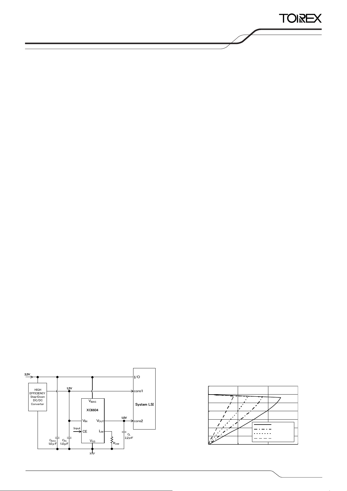
■TYPICAL APPLICATION CIRCUIT
pin.
LIM
). When the output current reaches the current limit, the output
L
pin quickly returns to the VSS level.
OUT
FEATURES
Maximum Output Current
ON Resistance
Bias Voltage Range
Input Voltage Range
Output Voltage Range
Output Voltage Accuracy
Ripple Rejection
Low Power Consumption
Stand-by Current
Under-voltage Lockout
Thermal Shutdown
Protection Circuit
Function
CE Pull-Down (Active High)
C
Operating Ambient Temperature
Output Capacitor
Packages
Environmentally Friendly
1A (1.3A Limit)
:
: 0.15Ω@V
: 2.5V~6.0V
: 0.5V~3.0V
: 0.5V~1.8V (0.1V increments)
: ±0.015V@V
±0.020V@V
: 60dB@f=1kHz (V
75dB@f=1kHz (V
: 100μA (V
: 0.01μA (V
1.8V (V
:
: 150℃@detect, 125℃@release
Foldback Current Limit, TSD, UVLO
:
Soft-start
:
High Speed Discharge
L
: -40℃~+85℃
: Ceramic Capacitor Compatible (2.2μF)
USP-6C, SOT-26W
:
EU RoHS Compliant, Pb Free
:
=3.6V, V
BIAS
<1.2V
OUT
≧1.2V
OUT
), 6.5μA (VIN)@V
BIAS
), 0.01μA (VIN)
BIAS
), 0.4V (VIN)
BIAS
OUT
BIAS_PSRR
IN_PSRR
■TYPICAL PERFORMANCE
CHARACTERISTICS
XC6604x121MR-G
1.4
1.2
(V)
OUT
1
0.8
0.6
0.4
0.2
Output Voltage: V
0
0.0 0.5 1.0 1.5
C
BIAS=CIN
Output Current: I
V
=3.6V, VIN=1.5V
BIAS=VCE
=1.0μF, CL=2.2μF, Ta=25℃
RLIM2=0kΩ
RLIM2=22kΩ
RLIM2=56kΩ
RLIM2=120kΩ
(A)
OUT
=1.2V
)
)
OUT
=1.2V
1/30
Page 2
XC6604 Series
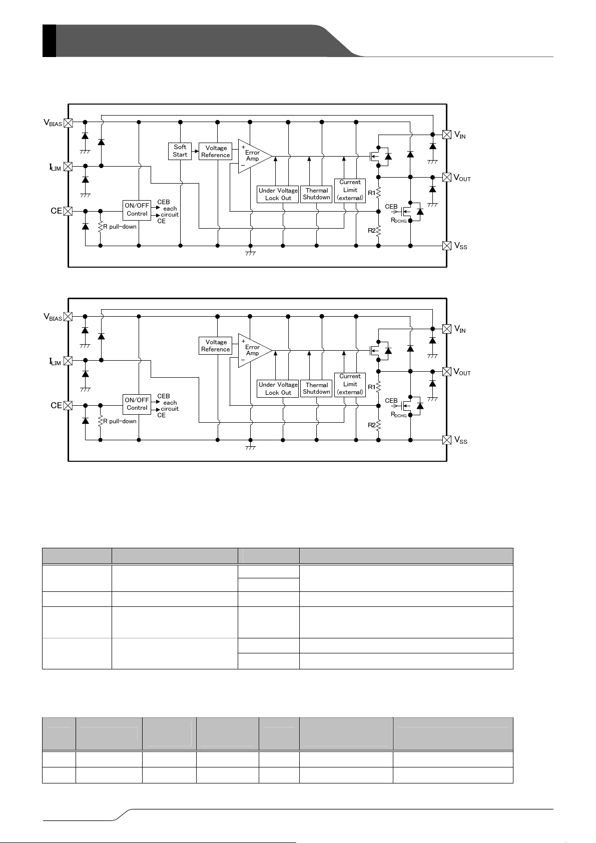
■BLOCK DIAGRAMS
Type A
Type B
■PRODUCT CLASSIFICATION
●Ordering Information
XC6604①②③④⑤⑥-⑦
DESIGNATOR ITEM SYMBOL DESCRIPTION
①
②③
④
⑤⑥-⑦
(*1)
The “-G” suffix denotes Halogen and Antimony free as well as being fully RoHS compliant.
(*1)
Output Voltage Accuracy 1
Packages (Order Unit)
Type
Output Voltage
●Selection Guide
TYPE SOFT-START
CURRENT
LIMITTER
THERMAL
SHUTDOWN
A Yes Adjustable Yes Yes Yes Yes
B No Adjustable Yes Yes Yes Yes
A
B
Refer to Selection Guide
05~18 e.g. 1.2V → ②=1, ③=2
±0.015V (V
<1.2V), ±0.020V (V
OUT
ER-G USP-6C (3,000/Reel)
MR-G SOT-26W (3,000/Reel)
UVLO
CE PULL-DOWN
RESISTOR
≧1.2V)
OUT
CL AUTO DISCHARGE
2/30
Page 3
XC6604
Series
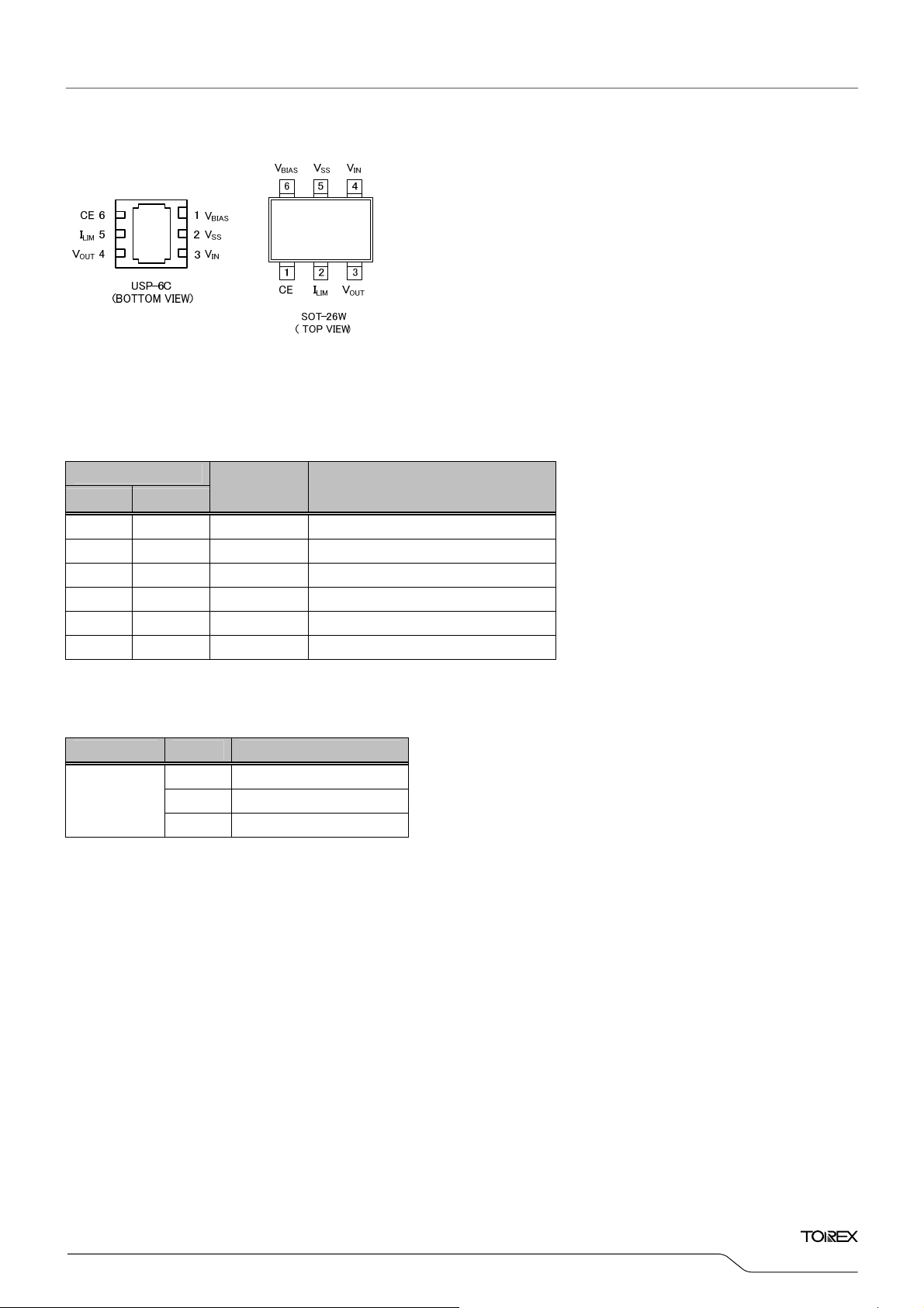
■PIN CONFIGURATION
*The dissipation pad for the USP-6C package should be solder-plated in recommended mount pattern and metal masking so as to enhance
mounting strength and heat release. If the pad needs to be connected to other pins, it should be connected to the V
(No. 2) pin.
SS
■PIN ASSIGNMENT
PIN NUMBER
PIN NAME FUNCTIONS
USP-6C SOT-26W
1 6 V
Power Supply Input
BIAS
2 5 VSS Ground
3 4 VIN Driver Transistor Input
4 3 V
5 2 I
Output
OUT
Current Limit Resistance Connection
LIM
6 1 CE ON/OFF Control
■FUNCTION CHART
PIN NAME SIGNAL STATUS
L Stand-by
CE
H Active
OPEN Stand-by
3/30
Page 4
XC6604 Series
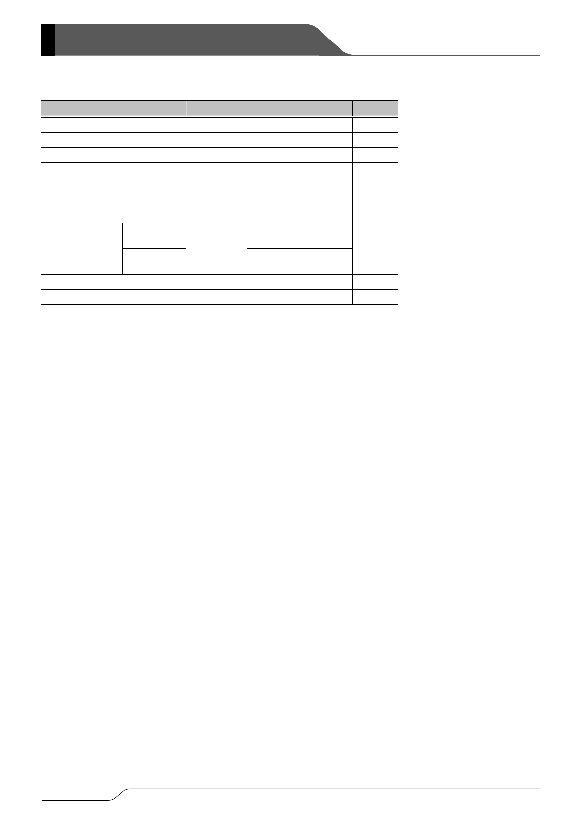
■ABSOLUTE MAXIMUM RATINGS
PARAMETER SYMBOL RATINGS UNITS
Ta =2 5℃
Bias Voltage V
Input Voltage VIN
Output Current I
Output Voltage
(*2)
V
CE Input Voltage VCE
I
Pin Voltage
LIM
(*3)
I
USP-6C
Power Dissipation
SOT-26W
Operating Ambient Temperature Topr
Storage Temperature Tstg
* All voltages are described based on the VSS pin.
(*1)
I
≦Pd/(VIN-V
OUT
(*2)
The maximum value should be either V
(*3)
The maximum value should be either VIN+0.3 or +6.5 in the lowest.
(*4)
The power dissipation measured with the test board condition is listed as reference data.
Please refer to page 26〜27 for details.
OUT
)
BIAS
BIAS
-0.3~+6.5
-0.3~+6.5
OUT
OUT
-0.3~V
-0.3~VIN+0.3 or +6.5
(*1)
1.65
+0.3 or +6.5
BIAS
-0.3~+6.5
LIM
Pd
-0.3~VIN+0.3 or +6.5
120
1000 (PCB mounted)
250
600 (PCB mounted)
-40~+85 ℃
-55~+125 ℃
+0.3, VIN+0.3 or +6.5 in the lowest.
(*4)
(*4)
V
V
A
V
V
V
mW
4/30
Page 5
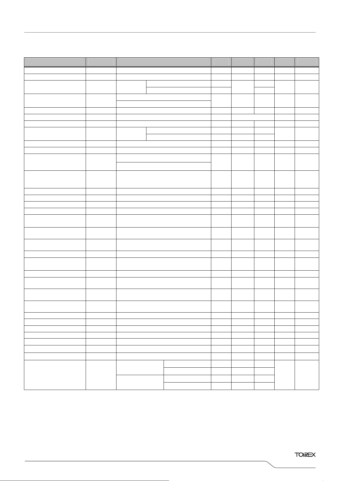
■ELECTRICAL CHARACTERISTICS
PARAMETER SYMBOL CONDITIONS MIN. TYP. MAX. UNITS CIRCUIT
Bias Voltage V
Input Voltage V
Output Voltage V
(*3
Maximum Output Current
)
I
Load Regulation ΔV
Dropout Voltage Vdif
Supply Current 1
(*6)
I
Supply Current 2 IIN I
Stand-by Current 1 I
Stand-by Current 2 I
Bias Line Regulation
Input Line Regulation
Bias UVLO Voltage V
Bias UVLO Release Voltage
Input UVLO Voltage VIN_
Input UVLO Release Voltage
Output Voltage
Temperature Characteristics
Bias Ripple Rejection R
atio V
Input Ripple Rejection Ratio
Current Limit
Adjustable Current
Limit Accuracy
(*3)
I
(*8)
Short - Circuit Current I
Thermal Shutdown
Detect Temperature
Thermal Shutdown
Release Temperature
Thermal Shutdown
Hysteresis Width
CL Auto-Discharge Resistance
CE "H" Level Voltage V
CE "L" Level Voltage V
CE "H" Level Current I
CE "L" Level Current I
Soft-Start Time
Output Rise Time
(*7)
(Type A) tSS
(*7)
(Type B) tON
Inrush Current (Type A) I
NOTE:
Unless otherwise stated, V
(*1)
V
= Effective output voltage
OUT(E)
(*2)
V
= Nominal output voltage
OUT(T)
(*3)
Mount conditions affect heat dissipation. Maximum output current is not guaranteed when TSD starts to operate earlier.
(*4)
Vdif={V
(*5)
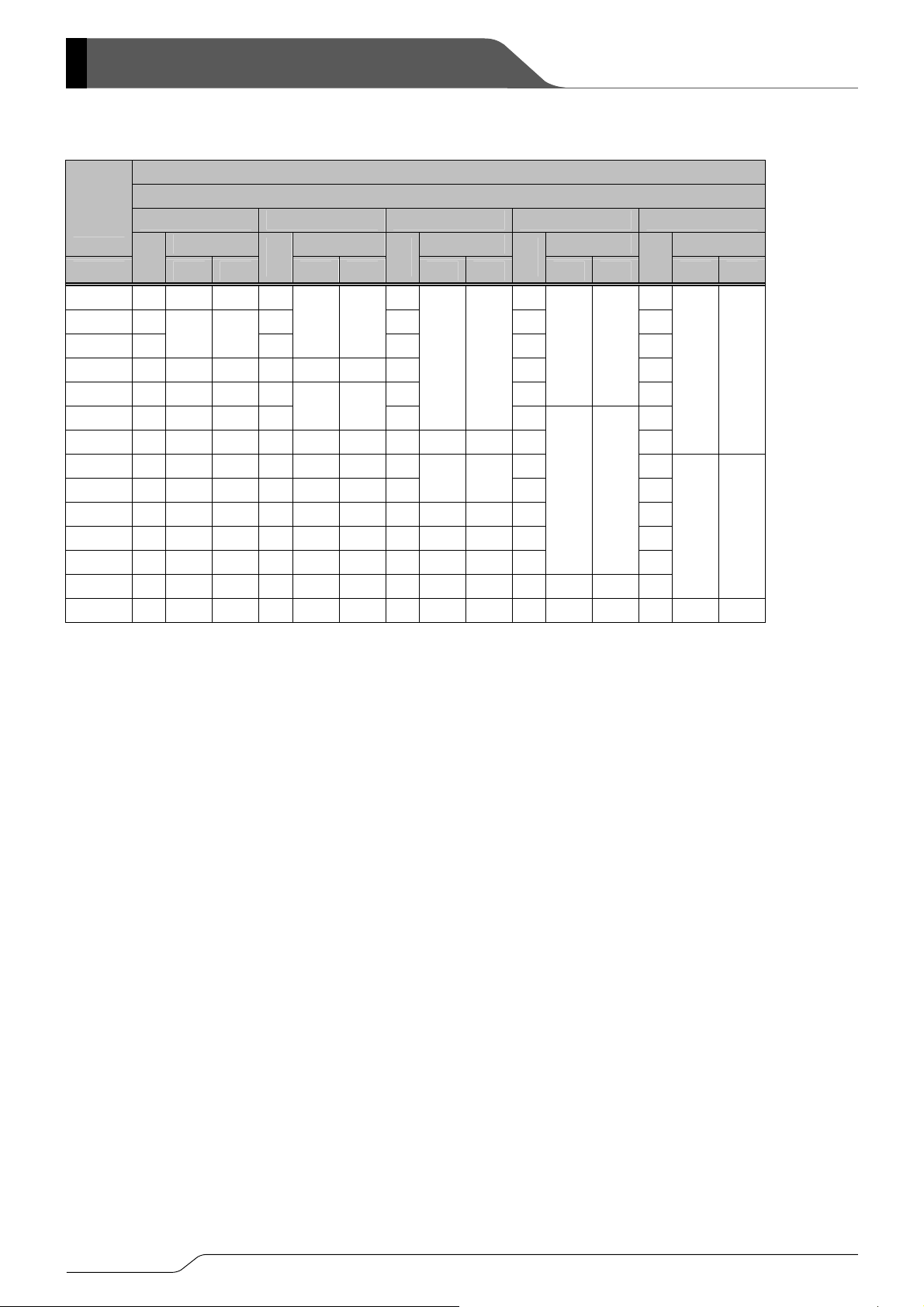
Please refer to the table E-1 named DROPOUT VOLTAGE CHART
(*6)
Supply current 1 (I
(*7)
A time between the CE input goes over the CE H threshold and the output reaches VOUT(E)x0.9V.
(*8)
Design value
IN1-VOUT1
V
is an input voltage when V
IN1
V
is a voltage equal to 98% of the output voltage where V
OUT1
BIAS=VCE
}
) may be fluctuated because that some bias current flows into the output.
BIAS
2.5 - 6.0 V ①
BIAS
0.5 - 3.0 V ①
IN
V
<1.2V -0.015 +0.015
(*1)
I
OUT(E)
OUTMAX
1mA≦I
OUT
(*4)
I
I
BIAS
V
BIAS_STB
V
IN_STB
ΔV
/
OUT
(ΔV
・
V
BIAS
OUT
ΔV
/
OUT
(ΔVIN・
V
)
OUT
BIAS_UVLOD
V
BIAS_UVLOR
UVLOD
VIN_
UVLOR
ΔV
/
OUT
・
V
(ΔTopr
OUT
BIAS_PSRR
V
IN_PSRR
V
LIM
I
- (-35) - (35) %
LIM_ADJ
V
SHORT
T
Junction Temperature - 150 - ℃ ①
TSD
T
Junction Temperature - 125 - ℃ ①
TSR
T
TSD-TTSR
R
VCE=VSS, V
DCHG
0.65 - 6.00 V ④
CEH
V
CEL
V
CEH
V
CEL
RUSH
=3.6V, VIN=V
OUT1
=100mA
OUT
V
<1.2V, V
OUT(T)
V
≧1.2V, V
OUT(T)
OUT
=1A - E-1
OUT
=0A 76 100 143 μA ②
OUT
=0A
OUT
=6.0V, VIN=3.0V, VCE=VSS - 0.01 0.10 μA ②
BIAS
=6.0V, VIN=3.0V, VCE=VSS - 0.01 0.15 μA ②
BIAS
V
<
1.2V, VCE=V
OUT(T)
)
V
≧
1.2V, VCE=V
OUT(T)
V
+0.1V≦VIN≦3.0V - 0.01 0.10 %/V ①
OUT(T)
V
2.5 - 6.0 V ①
V
0.5 - 3.0 V ①
I
=100mA
OUT
)
-40℃≦Topr≦85℃
V
BIAS=VCE
I
=100mA, f=1kHz, C
OUT
VIN=V
OUT(T)
I
=100mA, f=1kHz, CIN=OPEN
OUT
={V
OUT
OUT=VSS
Junction Temperature - 25 - ℃ ①
BIAS=VCE
=6.0V, VCE=V
BIAS
V
=0V→3.6V, tr=5μs
CE
V
=0V→3.6V, tr=5μs
CE
C
=2.2μF
L
C
=10μF
L
+0.3V, I
OUT(T)
appears at the output during decreasing input voltage gradually.
OUT(T)
V
≧1.2V -0.020
OUT(T)
=2.5V
BIAS=VCE
BIAS=VCE=VOUT(T)
+1.3V
1.0 - - A ①
≦1A - 37 68 mV ①
V
<1.2V 0.1 - 8.7
OUT(T)
V
≧1.2V 3.9 - 14.2
OUT(T)
, 2.5V
≦V
≦
BIAS
≦V
BIAS
6.0V
≦
6.0V
- 0.01 0.10 %/V ①
- 1.28 V ①
SS
- 0.23 V ①
SS
BIAS
BIAS
, V
OUT(T)
+1.3V
V
OUT(T)
(*2)
+0.020
(*5)
mV ①
- ±30 - ppm/℃ ①
=3.6VDC+0.2V
+0.3VDC+0.2V
OUT@IOUT
=1A}×0.95 1.0 1.3 - A ①
p-pAC
BIAS
p-pAC
=OPEN
- 60 - dB ③
- 75 - dB ③
- 90 - mA ①
OUT=VOUT(T)
130 190 255 Ω ①
- 0.41 V ④
SS
=6.0V 3.2 6.0 10.6 μA ④
-0.1 - 0.1 μA ④
SS
225 430 600
- - 110
- - 70
- - 85
- - 155
- - 215
Pin=VSS
LIM
OUT(T)
+0.3V at I
=1A is input to the VIN pin.
OUT
=1mA , C
OUT
V
OUT(T)
V
OUT(T)
V
OUT(T)
V
OUT(T)
BIAS=CIN
BIAS=VCE
≦1.2V
>1.2V
≦1.2V
>1.2V
=1.0μF, CL=2.2μF, I
=3.6 and VIN=V
XC6604
Series
Ta =2 5 ℃
V ①
μA ②
①
μs ⑤
μs ⑤
mA
⑤
5/30
Page 6
XC6604 Series
■ELECTRICAL CHARACTERISTICS (Continued)
●Dropout Voltage Chart
E-1
NOMINAL
OUTPUT
VOLTAGE
V
OUT(T)
0.5 2.5 152 218 2.8 3.1 3.7 4.5
0.6 2.4 2.7 3.0 3.6 4.4
0.7 2.3
0.8 2.2 158 228 2.5 152 218 2.8 3.4 4.2
0.9 2.1 162 233 2.4 2.7 3.3
1.0 2.0 165 238 2.3
1.1 1.9 167 243 2.2 158 228 2.5 152 218 3.1 3.9
1.2 1.8 169 253 2.1 162 233 2.4 3.0 3.8
1.3 1.7 179 268 2.0 165 238 2.3
1.4 1.6 189 283 1.9 167 243 2.2 158 228 2.8 3.6
1.5 1.5 202 303 1.8 169 253 2.1 162 233 2.7 3.5
1.6 1.4 213 328 1.7 179 268 2.0 165 238 2.6
1.7 1.3 225 373 1.6 189 283 1.9 167 243 2.5 152 218 3.3
1.8 1.2 255 423 1.5 202 303 1.8 169 253 2.4 155 223 3.2 146 213
* Dropout voltage is defined as the V
V
BIAS
VGS
(V)
TYP. MAX.
155 223
=3.0V V
Vdif(mV) Vdif(mV) Vdif(mV) Vdif(mV) Vdif(mV)
V
(V)
2.6
GS
=3.3V V
BIAS
GS
TYP. MAX.
146 213
155 223
(=V
BIAS–VOUT(E)
6/30
DROPOUT VOLTAGE (mV)
=3.6V V
BIAS
V
GS
(V)
TYP. MAX.
2.9 3.5 4.3
146 213
2.6
155 223
V
(V)
3.2 4.0
2.9 3.7
=4.2V V
BIAS
GS
TYP. MAX.
140 208
146 213
) of the driver transistor.
BIAS
VGS
(V)
TYP. MAX.
137 206
4.1
140 208
3.4
=5.0V
Page 7
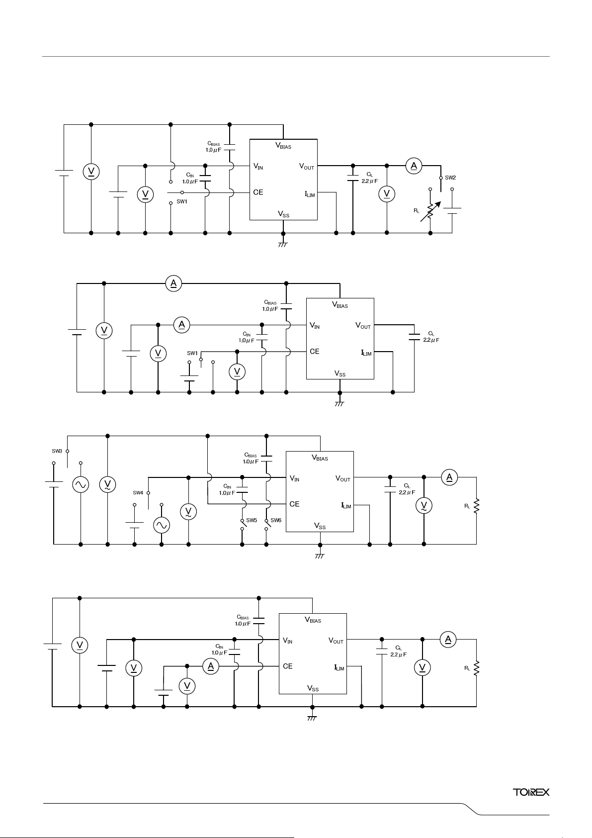
■TEST CIRCUITS
CIRCUIT①
CIRCUIT②
CIRCUIT③
CIRCUIT④
XC6604
Series
7/30
Page 8

XC6604 Series
■TEST CIRCUITS (Continued)
CIRCUIT⑤
8/30
XC6604 Series, Type A
XC6604 Series, Type B
Page 9
XC6604
Series
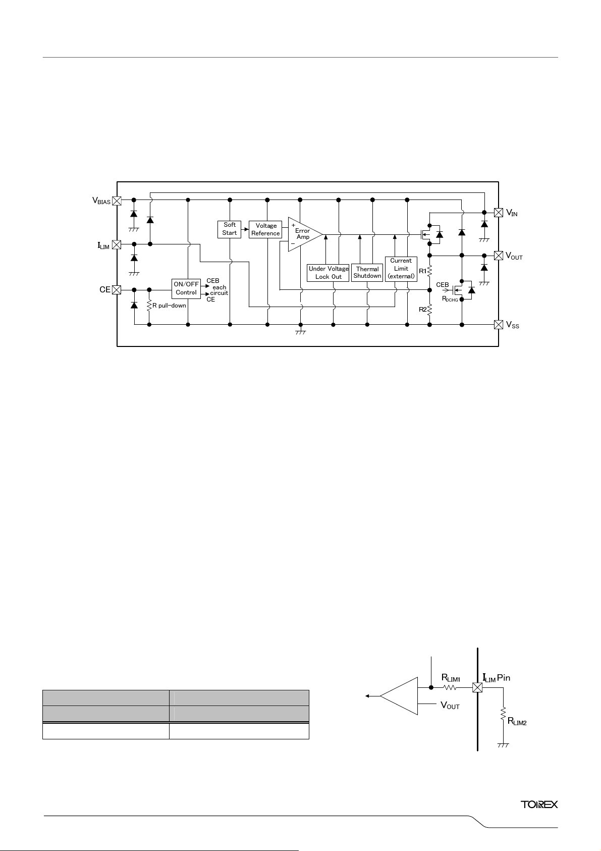
■OPERATIONAL DESCRIPTION
The voltage divided by resistors R1 and R2 is compared with the internal reference voltage by the error amplifier. The V
by the subsequent output signal. The output voltage at the V
V
pin is power supply pin for output voltage control circuit, protection circuit and CE circuit. Also, the V
BIAS
output current. V
pin is connected to a driver transistor and provides output current.
IN
In order to obtain high efficient output current through low on-resistance, please take enough V
pin is controlled and stabilized by a system of negative feedback.
OUT
pin supplies some current as
BIAS
(=V
BIAS
– V
GS
) of the driver transistor.
OUT(E)
Figure1: XC6604 Series, Type A
<Current Limiter, Short-Circuit Protection>
The XC6604 series includes a combination of a fixed current limiter circuit and a foldback short-circuit protection. When the output current
reaches the current limit, the output voltage drops and this operation makes the output current foldback to be decreased.
The current limit can be set freely with connecting a resistor to the I
LIM
pin.
Please note about the foldback circuit characteristics below;
●Output voltage may not rise when the output voltage is lower than 0V at the IC operation start.
●Current over the foldback current limit will not flow at the IC operation start.
●Please use type A (with soft-start time) to prevent from inrush current, because the circuit may not response to a drastic current change such
as the inrush current.
When the I
pin is left open, driver transistor will be forced off.
LIM
Current Limit is calculated by the following formulas.
= V
I
LIM
/ ( R
+ R
OUT(T
= V
R
LIM1
)
OUT(T
LIM1
)
) × 79645.7 [A]
LIM2
/ ( 16.3 × 10⁻⁶ ) [Ω]
: Current Limit
I
LIM
: Nominal Output Voltage
V
OUT(T)
: Internal Current Limit Resistance
R
LIM1
: External Current Limit Resistance
R
LIM2
Figure 2: XC6604 Series, Range of adjustable current limit
OUTPUT VOLTAGE RANGE ADJUSTABLE CURRENT LIMIT
V
I
OUT(T)
LIM
0.5V~1.8V 0.5A~1.3A
XC6604 Series, R
LIM2
pin is then driven
OUT
Connecting
9/30
Page 10
XC6604 Series
■OPERATIONAL DESCRIPTION (Continued)
<Soft-Start Function>
With the XC6604 (Type A), the inrush current (I
As for the XC6604, the soft-start time in the type A is optimized internally. On the other hand, the type B of the XC6604 does not have the
soft-start time function.
<Thermal Shutdown Circuit (TSD) >
When the junction temperature of the built-in driver transistor reaches the temperature limit, the thermal shutdown circuit operates and the
driver transistor will be set to OFF. The IC resumes its operation when the thermal shutdown function is released and the IC’s operation is
automatically restored because the junction temperature drops to the level of the thermal shutdown release temperature.
<Under Voltage Lock Out (UVLO) >
When the V
pin and VIN pin voltage drops, the output driver transistor is set to OFF by UVLO function to prevent false output caused by
BIAS
unstable operation of the internal circuitry. When the V
released. The driver transistor is turned ON and start to operate voltage regulation.
<CE Pin>
The XC6604 internal circuitry can be shutdown via the signal to the CE pin. In shutdown mode with CE low level voltage, the V
pulled down to the V
level via CL discharge resistance (R
SS
The CE pin has pull-down circuitry so that CE input current flows during IC operation. If the CE pin voltage is taken from V
then logic is fixed and the IC will operate normally. However, supply current may increase as a result of through current in the IC's internal
circuitry when medium voltage is input.
<C
High Speed Auto-Discharge>
L
XC6604 series can quickly discharge the electric charge at the output capacitor (C
and the V
the output capacitor (C
auto-discharge resistance (R
an output capacitor value (C
formula. Please also note R
pin when a low signal to the CE pin which enables a whole IC circuit put into OFF state. When the IC is disabled, electric charge at
SS
) is quickly discharged so that it could avoids malfunction. Discharge time of the output capacitor (CL) is set by the C
L
) and the output capacitor (CL). By setting time constant of a CL auto-discharge resistance value (R
DCHG
) as τ(τ= CL x R
L
is depended on V
DCHG
V: Output voltage during discharge
: Initial Output voltage
V
OUT(E)
t: Discharge time
τ: C
L×RDCHG
<Low ESR Capacitor>
With the XC6604 series, a stable output voltage is achievable even if used with low ESR capacitors, as a phase compensation circuit is built-in.
The output capacitor (C
) should be connected as close to V
L
phase compensation are as the table below.
For a stable power input, please connect a bias capacitor (C
) between the VIN pin and the VSS pin. In order to ensure the stable phase compensation while avoiding run-out of values, please use the
(C
IN
capacitor (C
of C
BIAS
, CIN and CL) which does not depend on bias or temperature too much. The table below (Figure 3) shows recommended values
BIAS
, CIN and CL.
Figure 3: Recommended Values of C
OUTPUT VOLTAGE
RANGE
V
C
OUT(T)
, CIN and CL (MIN.)
BIAS
BIAS CAPACITOR INPUT CAPACITOR
BIAS
0.5V~1.8V 1.0μF 1.0μF 2.2μF
) from VIN to V
RUSH
pin voltage and the VIN pin voltage rises at release voltage, the UVLO function is
BIAS
DCHG
), the output voltage after discharge via the internal transistor is calculated by the following
DCHG
. When V
BIAS
OUT(E)
×
BIAS
V = V
for charging CL at start-up can be reduced and makes the VIN stable.
OUT
) placed in parallel to R1 and R2.
BIAS
) via the internal transistor located between the V
L
is larger, R
BIAS
-t/
τ
e
or t=τln(V
pin and VSS pin to obtain stable phase compensation. Values required for the
OUT
) between the V
is smaller.
DCHG
/ V)
OUT(E)
pin and the VSS pin. Also, please connect an input capacitor
BIAS
OUTPUT
CAPACITOR
CIN CL
pin will be
OUT
pin or VSS pin
pin
OUT
) and
DCHG
L
10/30
Page 11

XC6604
Series
■NOTES ON USE
1. For temporary, transitional voltage drop or voltage rising phenomenon, the IC is liable to malfunction should the ratings be exceeded.
2. Where wiring impedance is high, operations may become unstable due to noise and/or phase lag depending on output current. Please keep
the resistance low for the V
3. Please wire the C
4. Capacitances of these capacitors (C
taken for capacitor selection to ensure stability of phase compensation from the point of ESR influence.
5. When it is used in a quite small input / output dropout voltage, output may go into unstable operation. Please test it thoroughly before using
it in production.
6. Torex places an importance on improving our products and their reliability.
We request that users incorporate fail-safe designs and post-aging protection treatment when using Torex products in their systems.
, CIN and CL as close to the IC as possible.
BIAS
, VIN and VSS wiring in particular.
BIAS
, C
BIAS
) are decreased by the influences of bias voltage and ambient temperature. Care shall be
IN, CL
11/30
Page 12
XC6604 Series
■TYPICAL PERFORMANCE CHARACTERISTICS
* Unless otherwise stated, V
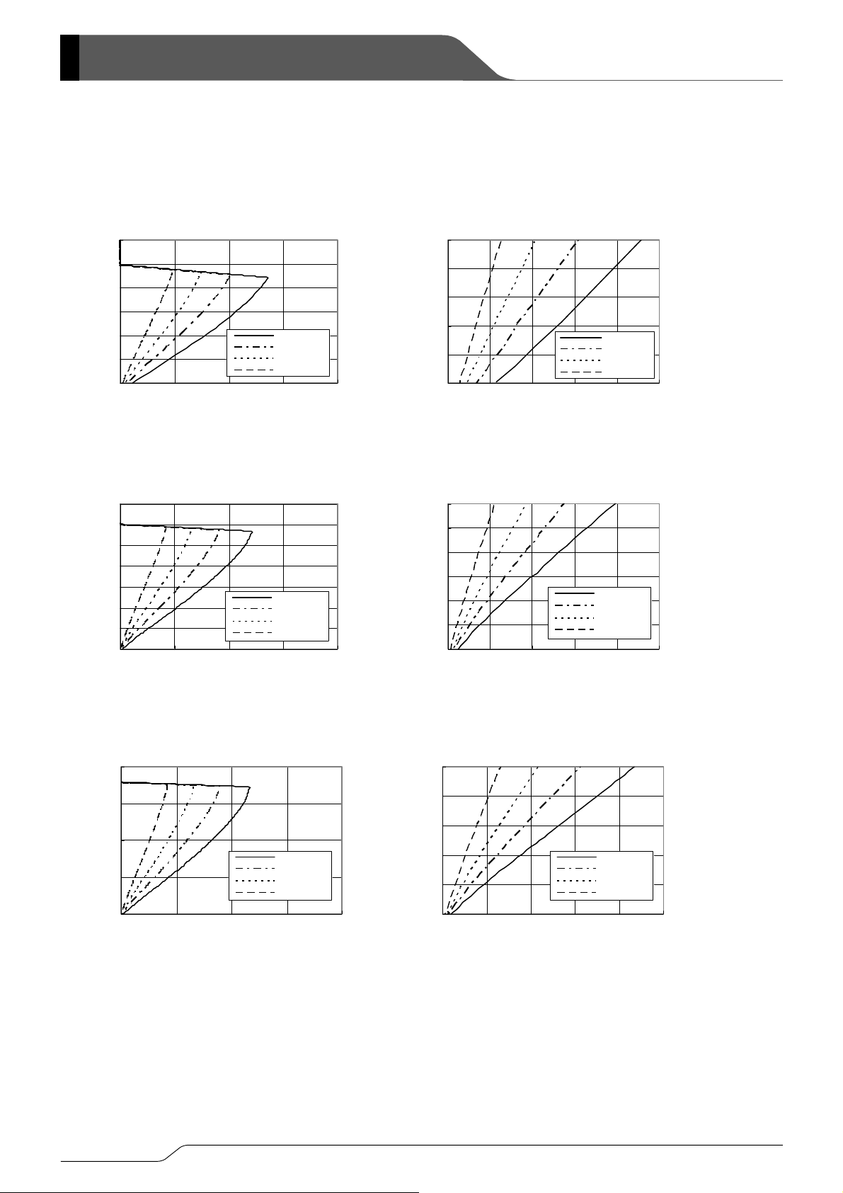
(1) Output Voltage vs. Output Current
XC6604x051MR-G
0.6
(V)
0.5
OUT
0.4
0.3
0.2
0.1
Output Voltage: V
0
0 0.5 1 1.5 2
Output Current: I
XC6604x121MR-G
1.4
1.2
(V)
OUT
1
0.8
0.6
0.4
0.2
Output Voltage: V
0
0 0.5 1 1.5 2
Output Current: I
XC6604x181MR-G
2
(V)
1.5
OUT
1
0.5
Output Voltage: V
0
00.511.52
Output Current: I
* Mount conditions affect heat dissipation. Thermal shutdown
may start to operate before reaching the current limit.
BIAS=VCE
=3.6V, VIN=V
RLIM2=0kΩ
RLIM2=9.1kΩ
RLIM2=22kΩ
RLIM2=47kΩ
(A)
OUT
RLIM2=0kΩ
RLIM2=22kΩ
RLIM2=56kΩ
RLIM2=120kΩ
(A)
OUT
RLIM2=0kΩ
RLIM2=33kΩ
RLIM2=82kΩ
RLIM2=180kΩ
A)
OUT(
OUT(T)
+0.3V, I
OUT
=1mA , I
Pin= VSS, C
LIM
=1.0μF, CL=2.2μF, Ta = 25 ℃
BIAS=CIN
XC6604x051MR-G
0.1
(V)
0.08
OUT
0.06
0.04
0.02
Output Voltage: V
0
0 0.1 0.2 0.3 0.4 0.5
Output Current: I
XC6604x121MR-G
0.3
0.25
(V)
OUT
0.2
0.15
0.1
0.05
Output Voltage: V
0
0 0.1 0.2 0.3 0.4 0.5
Output Current: I
XC6604x181MR-G
0.5
(V)
0.4
OUT
0.3
0.2
0.1
Output Voltage: V
0
0 0.1 0.2 0.3 0.4 0.5
Output Current: I
* If start-up current is required over the current limit, IC operation will not start.
Please use the current within the range of use.
RLIM2=0kΩ
RLIM2=9.1kΩ
RLIM2=22kΩ
RLIM2=47kΩ
(A)
OUT
RLIM2=0kΩ
RLIM2=22kΩ
RLIM2=56kΩ
RLIM2=120kΩ
(A)
OUT
RLIM2=0kΩ
RLIM2=33kΩ
RLIM2=82kΩ
RLIM2=180kΩ
A)
OUT(
12/30
Page 13
■TYPICAL PERFORMANCE CHARACTERISTICS (Continued)
* Unless otherwise stated, V
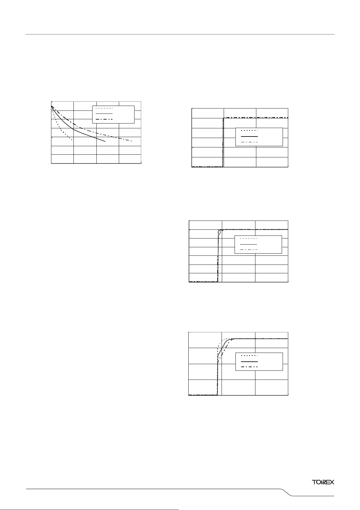
(2) Limit Current vs. Adjustable Resistance (3) Output Voltage vs. Bias Voltage
XC6604xxx1xR-G
1.4
1.2
(A)
1
LIM
0.8
0.6
0.4
Limit Current: I
0.2
0
0 50 100 150 200
Adjustable Resistance: R
BIAS=VCE
=3.6V, VIN=V
VOUT(T)=0 .5V
VOUT(T)=1 .2V
VOUT(T)=1 .8V
(kΩ)
LIM2
OUT(T)
+0.3V, I
OUT
=1mA, I
(V)
OUT
Output Voltage: V
(V)
OUT
Output Voltage: V
Pin= VSS, C
LIM
=1.0μF, CL=2.2μF, Ta = 25 ℃
BIAS=CIN
XC6604x051xR-G
0.6
(V)
0.5
OUT
0.4
0.3
IOUT=0mA
IOUT=1mA
IOUT=100mA
0.2
0.1
Output Voltage: V
0.0
0246
Bias Voltage: V
BIAS
(V)
XC6604x121xR-G
1.4
1.2
1.0
0.8
IOUT=0mA
IOUT=1mA
IOUT=100mA
0.6
0.4
0.2
0.0
0246
Bias Vo ltage: V
BIAS
(V)
XC6604x181xR-G
2.0
1.5
IOUT=0mA
1.0
IOUT=1mA
IOUT=100mA
0.5
0.0
0246
Bias Vo ltage: V
BIAS
(V)
XC6604
Series
13/30
Page 14
XC6604 Series
■TYPICAL PERFORMANCE CHARACTERISTICS (Continued)
* Unless otherwise stated, V
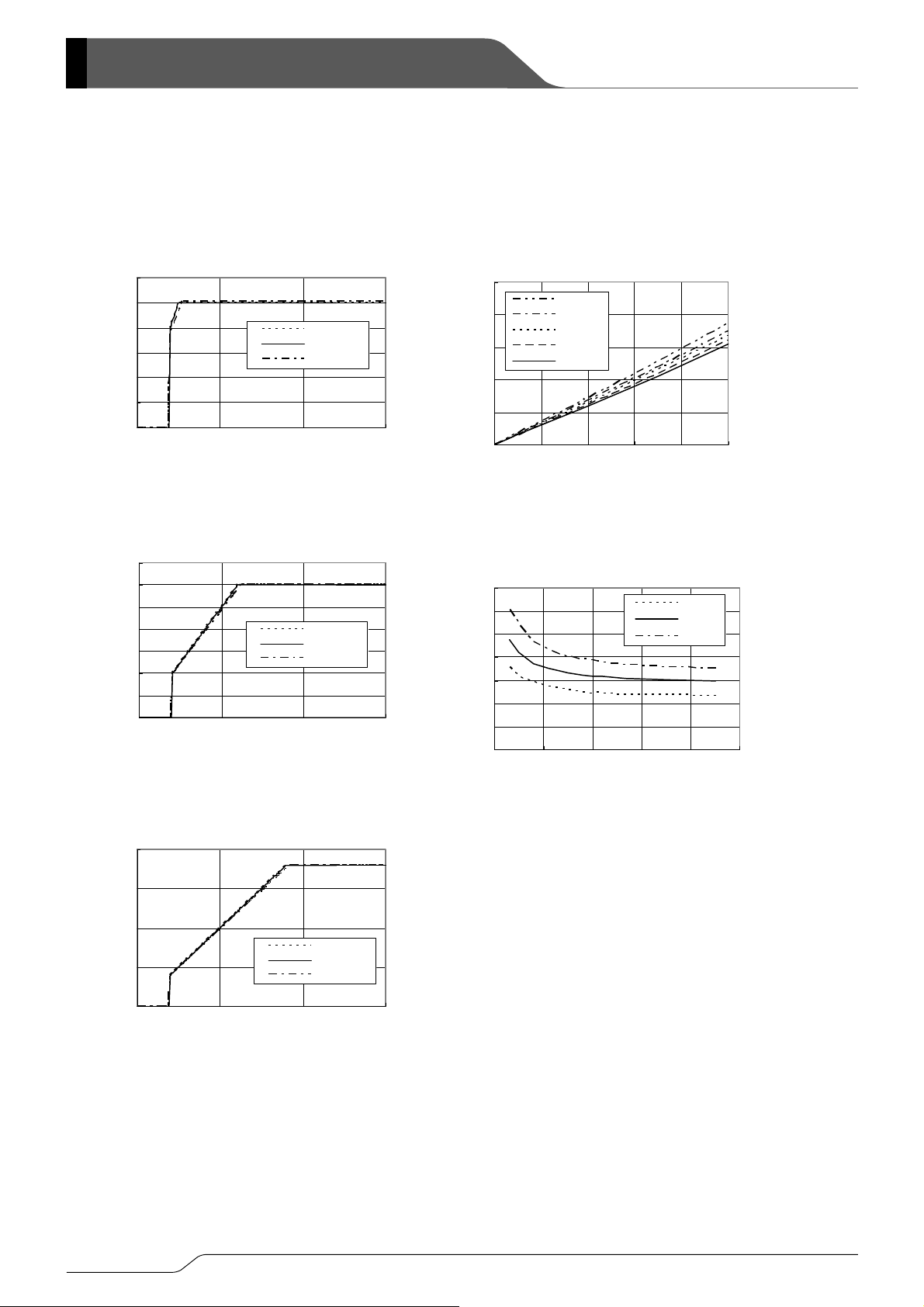
(4) Output Voltage vs. Input Voltage (5) Dropout Voltage vs. Output Current
XC6604x051xR-G
0.6
(V)
0.5
OUT
0.4
0.3
0.2
0.1
Output Voltage: V
0.0
0123
Input Voltage: V
XC6604x121xR-G
1.4
1.2
(V)
OUT
1.0
0.8
0.6
0.4
0.2
Output Voltage: V
0.0
0123
Input Voltage: V
XC6604x181xR-G
2.0
(V)
1.5
OUT
1.0
0.5
Output Voltage: V
0.0
0123
Input Voltage: V
BIAS=VCE
=3.6V, VIN=V
IOUT=0mA
IOUT=1mA
IOUT=100mA
(V)
IN
IOUT=0mA
IOUT=1mA
IOUT=100mA
(V)
IN
IOUT=0mA
IOUT=1mA
IOUT=100mA
(V)
IN
OUT(T)
+0.3V, I
OUT
=1mA, I
Pin=VSS, C
LIM
=1.0μF, CL=2.2μF, Ta = 25 ℃
BIAS=CIN
XC6604x121MR-G
250
VBIAS=3.0V
200
150
VBIAS=3.3V
VBIAS=3.6V
VBIAS=4.2V
VBIAS=5.0V
100
50
Dro pout Voltage : Vdif(mV)
0
0 200 400 600 800 1000
Output Current: I
OUT
(mA)
XC6604xxx1MR-G
I
OUT
350
300
250
Ta=-40℃
Ta=25℃
Ta=85℃
200
150
100
50
Dro pout Voltage : Vdif(mV)
0
123456
(*1)
(V)
V
GS
(*1)
VGS is a Gate –Source voltage of the driver transistor that is defined as
- V
the value of V
BIAS
OUT(E)
.
A value of the dropout voltage is determined by the value of the V
=1A
.
GS
14/30
Page 15
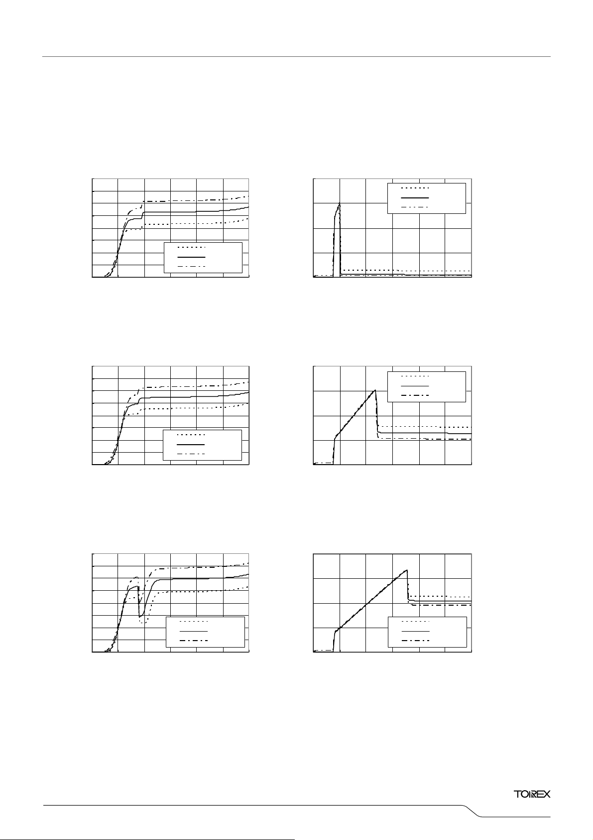
■TYPICAL PERFORMANCE CHARACTERISTICS (Continued)
* Unless otherwise stated, V
(6) Supply Bias Current vs. Bias Voltage (7) Supply Input Current vs. Input Voltage
XC6604x051xR-G
160
(μA)
140
BIA S
120
100
80
60
40
20
Su pply Bias Current: I
0
0123456
Bias Voltage: V
XC6604x121xR-G
160
(μA)
140
BIAS
120
100
80
60
40
20
Supply Bias Current: I
0
0123456
Bias Voltage: V
XC6604x181xR-G
160
(μA)
140
BIAS
120
100
80
60
40
20
Su pply Bias Current: I
0
0123456
Bias Voltage: V
BIAS=VCE
=3.6V, VIN=V
CIN=C
V
CE=VBIAS
Ta=-40℃
Ta=25℃
Ta=85℃
(V)
BIA S
CIN=C
V
CE=VBIAS, IOUT
Ta=-40℃
Ta=25℃
Ta=85℃
(V)
BIA S
CIN=C
V
CE=VBIAS
(V)
BIA S
OUT(T)
BIAS=CL
, I
BIAS=CL
BIAS=CL
, I
Ta=-40℃
Ta=25℃
Ta=85℃
+0.3V, I
=OPEN
=0mA
OUT
=OPEN
=0mA
=OPEN
=0mA,
OUT
OUT
=1mA, I
(μA)
IN
Su pply Input Curr e n t: I
(μA)
IN
Su pply Input Curr en t: I
(μA)
IN
Su pply Input Curr e n t: I
Pin=VSS, C
LIM
=1.0μF, CL=2.2μF, Ta = 25 ℃
BIAS=CIN
XC6604x051xR-G
CIN=C
20
Ta=-40℃
15
Ta=25℃
Ta=85℃
10
5
0
0 0.5 1 1.5 2 2 .5 3
Input Voltage: V
(V)
IN
XC6604x121xR-G
CIN=C
20
Ta=-40℃
15
Ta=25℃
Ta=85℃
10
5
0
0 0.5 1 1.5 2 2 .5 3
Input Voltage: V
(V)
IN
XC6604x181xR-G
CIN=C
20
15
10
5
Ta=-40℃
Ta=25℃
Ta=85℃
0
0 0.5 1 1.5 2 2 .5 3
Input Voltage: V
(V)
IN
BIAS=CL
BIAS=CL
BIAS=CL
=OPE N
I
OUT
=OPE N
I
OUT
=OPE N
I
OUT
XC6604
Series
=0mA
=0mA
=0mA
15/30
Page 16
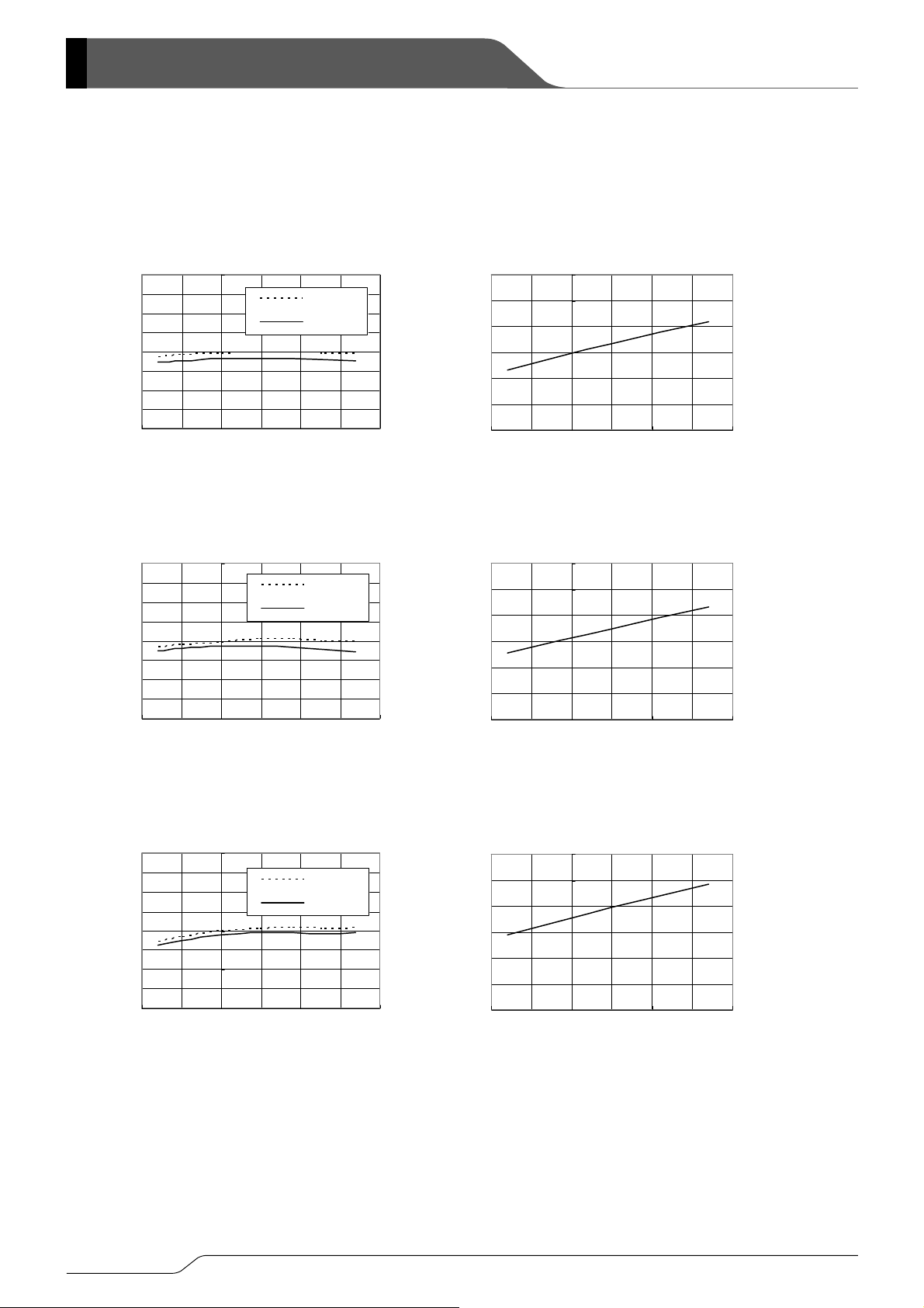
XC6604 Series
■TYPICAL PERFORMANCE CHARACTERISTICS (Continued)
* Unless otherwise stated, V
(8) Output Voltage vs. Ambient Temperature (9) Supply Bias Current vs. Ambient Temperature
XC6604x051xR-G
0.52
(V)
0.51
OUT
0.5
0.49
Output Voltage: V
0.48
-50 0 50 100
Ambient Temperature: Ta(℃)
XC6604x121xR-G
1.22
(V)
1.21
OUT
1.2
1.19
Output Voltage: V
1.18
-50 0 50 100
Ambient Temperature: Ta(℃)
XC6604x181xR-G
1.82
(V)
1.81
OUT
1.8
1.79
Output Voltage: V
1.78
-50 0 50 100
Ambient Temperature: Ta(℃)
BIAS=VCE
=3.6V, VIN=V
IOUT=1mA
IOUT=100mA
IOUT=1mA
IOUT=100mA
IOUT=1mA
IOUT=100mA
OUT(T)
+0.3V, I
OUT
=1mA, I
(μA)
BIAs
Su pply Bias Cu rre n t: I
(μA)
BIAs
Supply Bias Current: I
(μA)
BIAs
Supply Bias Current: I
Pin=VSS, C
LIM
=1.0μF, CL=2.2μF, Ta = 25 ℃
BIAS=CIN
XC6604x051xR-G
CIN=C
BIAS=CL
160
140
120
100
80
60
40
-50 0 50 100
Ambient Temperature: Ta(℃)
XC6604x121xR-G
CIN=C
BIAS=CL
160
140
120
100
80
60
40
-50 0 50 100
Ambient Temperature: Ta(℃)
XC6604x181xR-G
CIN=C
BIAS
160
140
120
100
80
60
40
-50 0 50 100
Ambient Temperature: Ta(℃)
=OPE N
I
=0mA
OUT
=OPE N
I
=0mA
OUT
= CL=OPE N
I
=0mA
OUT
16/30
Page 17
A
A
A
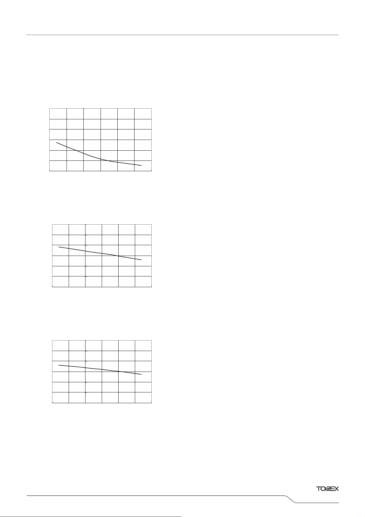
■TYPICAL PERFORMANCE CHARACTERISTICS (Continued)
* Unless otherwise stated, V
(10) Supply Input Current vs. Ambient Temperature
XC6604x051xR-G
3
(μA)
IN
2
1
Supply Input Current: I
0
-50 0 50 100
Ambient Temperature: Ta(℃)
XC6604x121xR-G
12
(μA)
10
IN
8
6
4
2
Supply Input Current: I
0
-50 0 50 100
Ambient Temperature: Ta(℃)
XC6604x181xR-G
16
(μA)
14
IN
12
10
8
6
Supply Input Current: I
4
-50 0 50 100
Ambient Temperature: Ta(℃)
BIAS=VCE
=3.6V, VIN=V
CIN=C
CIN=C
CIN=C
OUT(T)
BIAS=CL
BIAS=CL
BIAS=CL
+0.3V, I
=OPEN
I
=0m
OUT
=OPEN
I
=0m
OUT
=OPEN
I
=0m
OUT
OUT
=1mA, I
Pin=VSS, C
LIM
=1.0μF, CL=2.2μF, Ta = 25 ℃
BIAS=CIN
XC6604
Series
17/30
Page 18
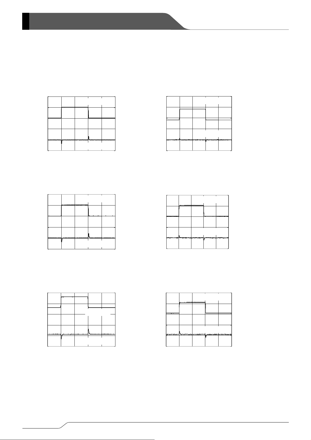
XC6604 Series
■TYPICAL PERFORMANCE CHARACTERISTICS (Continued)
* Unless otherwise stated, V
(11) Bias Transient Response (12) Input Transient Response
0.58
XC6604x051xR-G
V
BIAS
(V)
0.56
OUT
0.54
0.52
0.5
Output Voltage: V
0.48
Time (200μs/ div)
XC6604x121xR-G
V
BIAS
1.28
(V)
1.26
OUT
1.24
1.22
1.2
Output Voltage: V
1.18
Time (200μs/ div)
XC6604x181xR-G
V
=3.6V→4.6V(tr=tf=5μs) I
BIAS
1.88
(V)
1.86
OUT
1.84
1.82
1.8
Output Voltage: V
1.78
Time (200μs/div)
=3.6V, VIN=V
BIAS=VCE
=3.0V→4.0V(tr=tf=5μs), I
Bias Voltage
Output Voltage
=3.0V→4. 0V(tr=tf=5μs) I
Bias Voltage
Output Voltage
C
Bias Voltage
Output Voltage
C
C
OUT
BIAS
OUT
OUT(T)
=OPEN
BIAS
=100mA
OUT
=OPEN
BIAS
=100mA
=OPEN
=100mA
+0.3V, I
5
4
3
2
1
0
5
4
3
2
1
0
5
4
3
2
1
0
OUT
=1mA, I
Pin=VSS, C
LIM
=1.0μF, CL=2.2μF, Ta = 25 ℃
BIAS=CIN
XC6604x051xR-G
CIN=OPE N
=100mA
OUT
3
0.58
V
=0.8V→1.8V(tr=tf=5μs), I
IN
Input Voltage
(V)
(V)
BIAS
OUT
0.56
0.54
0.52
2
1
0
Output Voltage
Bias Voltage: V
0.5
Output Voltage: V
0.48
-1
-2
Time (200μs/ div)
XC6604x121xR-G
CIN=OPEN
=100mA
OUT
3.5
1.28
V
=1.5V→2. 5V(tr=tf=5μs), I
IN
Input Voltage
(V)
(V)
BIA S
OUT
1.26
1.24
1.22
Bias Voltage: V
1.2
Output Voltage: V
Output Voltage
1.18
2.5
1.5
0.5
-0.5
-1.5
Time (200μs/div)
XC6604x181xR-G
V
=2.1V→3.1V(tr=tf=5μs), I
IN
1.88
(V)
(V)
BIAS
OUT
1.86
Input Voltage
1.84
1.82
CIN=OPE N
=100mA
OUT
4
3
2
1
Output Voltage
Bias Voltage: V
1.8
Output Voltage: V
1.78
0
-1
Time (200μs/div)
(V)
IN
Input Voltage: V
(V)
IN
Input Voltage: V
(V)
IN
Input Voltage: V
18/30
Page 19
)
)
)
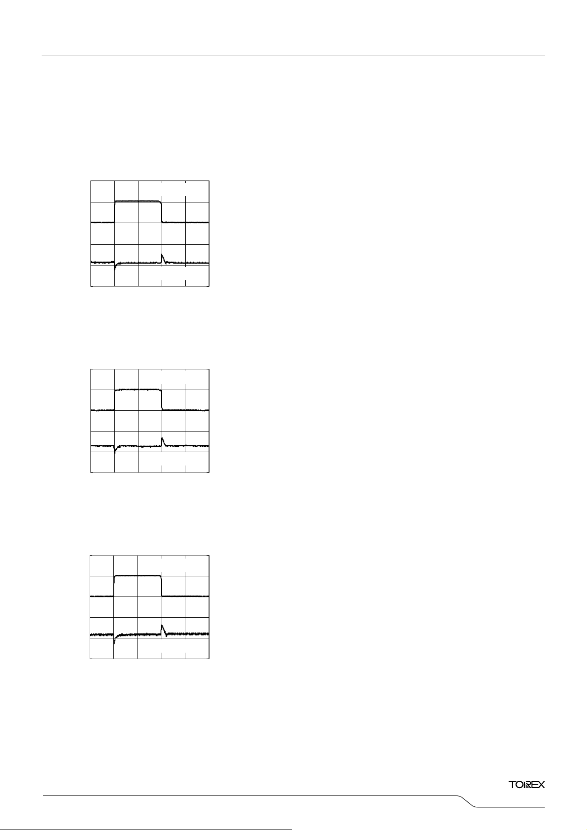
■TYPICAL PERFORMANCE CHARACTERISTICS (Continued)
* Unless otherwise stated, V
(13) Load Transient Response
XC6604x051xR-G
0.66
(V)
0.62
OUT
0.58
0.54
0.5
Output Voltage: V
0.46
Time (200μs/div)
XC6604x121xR-G
1.36
(V)
1.32
OUT
1.28
1.24
1.2
Output Voltage: V
1.16
Time (200μs/div)
XC6604x181xR-G
1.96
(V)
1.92
OUT
1.88
1.84
Output Voltage: V
1.8
1.76
Time (200μs/div)
=3.6V, VIN=V
BIAS=VCE
I
=1mA⇔100mA(tr=tf=5μs
OUT
Output Current
Output Voltage
I
=1mA⇔100mA(tr=tf=5μs
OUT
Output Current
Output Voltage
I
=1mA⇔100mA(tr=tf=5μs
OUT
Output Current
Output Voltage
OUT(T)
0.2
0.1
0
-0.1
-0.2
-0.3
0.2
0.1
0
-0.1
-0.2
-0.3
0.2
0.1
0
-0.1
-0.2
-0.3
+0.3V, I
(A)
OUT
Outpur Current: I
(A)
OUT
Outpur Current: I
(A)
OUT
Outpur Current: I
OUT
=1mA, I
Pin=VSS, C
LIM
=1.0μF, CL=2.2μF, Ta = 25 ℃
BIAS=CIN
XC6604
Series
19/30
Page 20
)
A
)
)
A
)
)
)
XC6604 Series
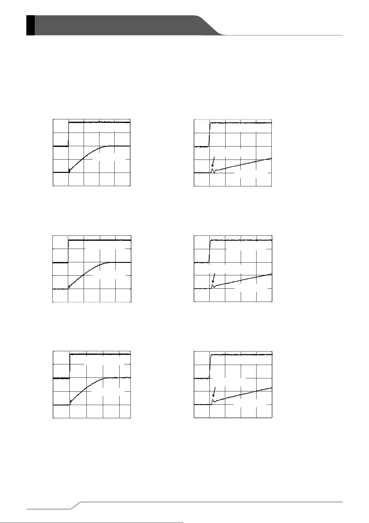
■TYPICAL PERFORMANCE CHARACTERISTICS (Continued)
* Unless otherwise stated, V
(14) CE Input Response
XC6604A051xR-G
4
(V)
2
CE
0
-2
-4
CE Input Voltage: V
-6
Time (200μs/div)
XC6604A121xR-G
4
(V)
2
CE
0
-2
-4
CE Input Voltage: V
-6
Time (200μs/div)
XC6604A181xR-G
4
(V)
2
CE
0
-2
-4
CE Input Voltage: V
-6
Time (200μs/div)
CE Input Voltage
CE Input Voltage
CE Input Voltage
=3.6V, VIN=V
BIAS=VCE
Input Current
VCE=0V→3.6V(tr=5μs
Input Current
VCE=0V→3.6V(tr=5μs
Input Current
OUT(T)
VCE=0V→3.6V(tr=5μs
I
=100mA
OUT
200
150
100
50
0
-50
I
=100mA
OUT
200
150
100
50
0
-50
I
=100mA
OUT
200
150
100
50
0
-50
+0.3V, I
(mA)
IN
Input Current: I
(mA)
IN
Input Current: I
(mA)
IN
Input Current: I
OUT
=1mA, I
Pin= VSS, C
LIM
4
(V)
2
CE
0
-2
-4
CE Input Voltage: V
-6
4
(V)
2
CE
0
-2
-4
CE Input Voltage: V
-6
4
(V)
2
CE
0
-2
-4
CE Input Voltage: V
-6
=1.0μF, CL=2.2μF, Ta = 25 ℃
BIAS=CIN
XC6604A051xR-G
CE Input Voltage
Rush Current
Input Current
Time (50μs/div)
XC6604A121xR-G
CE Input Voltage
Rush Current
Input Current
Time (50μs/div)
XC6604A181xR-G
CE Input Voltage
Rush Current
Input Current
Time (50μs/div)
VCE=0V→3.6V(tr=5μs
I
=100m
OUT
200
150
100
50
0
-50
VCE=0V→3.6V(tr=5μs
I
=100mA
OUT
200
150
100
50
0
-50
VCE=0V→3.6V(tr=5μs
I
=100m
OUT
200
150
100
50
0
-50
(mA)
IN
Input Current: I
(mA)
IN
Input Current: I
(mA)
IN
Input Current: I
20/30
Page 21
F
F
F
F
F
F
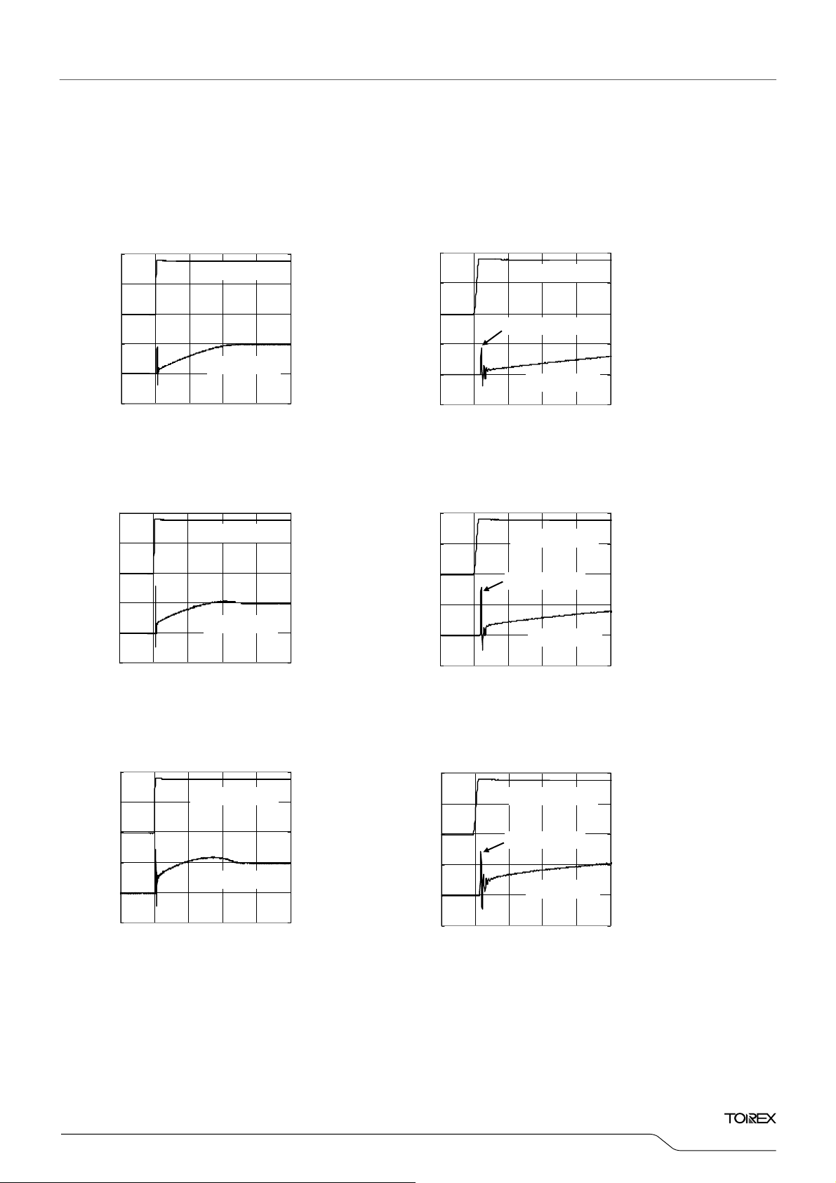
■TYPICAL PERFORMANCE CHARACTERISTICS (Continued)
* Unless otherwise stated, V
(14) CE Input Response (Continued)
XC6604A051xR-G
4
(V)
2
CE
CE In put Voltage
0
-2
-4
CE In put Voltage : V
-6
Time (200μs/div)
XC6604A121xR-G
4
(V)
2
CE
0
VCE=0V→3.6V(tr=5μs), I
CE Input Voltage
-2
-4
CE In put Voltage : V
-6
Time (200μs/div)
XC6604A181xR-G
4
VCE=0V→3.6V(tr=5μs), I
(V)
2
CE
CE Input Voltage
0
-2
-4
CE Input Voltage: V
-6
Time (200μs/div)
=3.6V, VIN=V
BIAS=VCE
VCE=0V→3.6V(tr=5μs), I
Input Current
Input Current
Input Current
OUT
CL=10μ
=100mA
OUT
CL=10μ
=100mA
OUT
OUT(T)
CL=10μ
=100mA
400
300
200
100
0
-100
400
300
200
100
0
-100
400
300
200
100
0
-100
+0.3V, I
(mA)
IN
Input Current: I
(mA)
IN
Input Current: I
(mA)
IN
Input Current: I
OUT
=1mA, I
Pin=VSS, C
LIM
4
(V)
2
CE
0
-2
-4
CE In put Voltage : V
-6
4
(V)
2
CE
0
-2
-4
CE In put Voltage : V
-6
4
(V)
2
CE
0
-2
-4
CE Input Voltage: V
-6
=1.0μF, CL=2.2μF, Ta = 25 ℃
BIAS=CIN
XC6604A051xR-G
VCE=0V→3.6V(tr=5μs), I
CE Input Voltage
Rush Current
Input Current
Time (50μs/div)
XC6604A121xR-G
VCE=0V→3.6V(tr=5μs), I
CE Input Voltage
Rush Current
Input Current
Time (50μs/div)
XC6604A181xR-G
VCE=0V→3.6V(tr=5μs), I
CE In put Voltage
Rush Current
Input Current
Time (5 0 μs/div)
OUT
CL=10μ
=100mA
OUT
CL=10μ
=100mA
OUT
CL=10μ
=100mA
400
300
200
100
0
-100
400
300
200
100
0
-100
400
300
200
100
0
-100
XC6604
Series
(mA)
IN
Input Current: I
(mA)
IN
Input Current: I
(mA)
IN
Input Current: I
21/30
Page 22
)
A
)
)
)
)
)
XC6604 Series
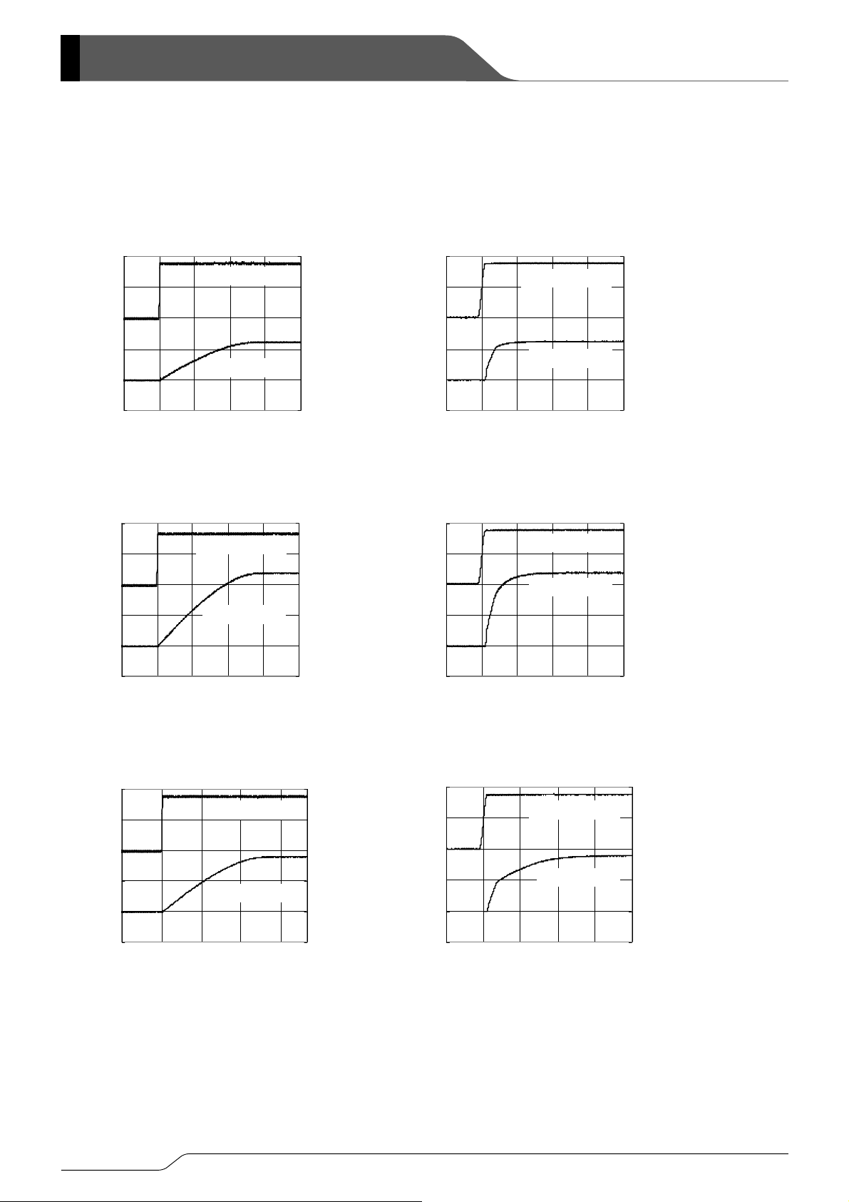
■TYPICAL PERFORMANCE CHARACTERISTICS (Continued)
* Unless otherwise stated, V
(15) CE Rising Response Time
XC6604A051xR-G
4
(V)
2
CE
0
-2
-4
CE Input Voltage: V
-6
Time (200μs/div)
XC6604A121xR-G
4
(V)
2
CE
CE Input Voltage
0
-2
-4
CE Input Voltage: V
-6
Time (200μs/div)
XC6604A181xR-G
4
(V)
2
CE
0
-2
-4
CE Input Voltage: V
-6
Time (200μs/div)
=3.6V, VIN=V
BIAS=VCE
VCE=0V→3.6V(tr=5μs
CE Input Voltage
Output Voltage
VCE=0V→3.6V(tr=5μs
Output Voltage
VCE=0V→3.6V(tr=5μs
CE Input Voltage
Output Voltage
I
OUT
I
OUT
I
=100m
=100mA
2
1.5
1
0.5
0
-0.5
=100mA
OUT
OUT(T)
1.6
1.2
0.8
0.4
0
-0.4
4
3
2
1
0
-1
+0.3V, I
(V)
OUT
Output Voltage: V
(V)
OUT
Output Voltage: V
(V)
OUT
Output Voltage: V
OUT
=1mA, I
Pin=VSS, C
LIM
4
(V)
2
CE
0
-2
-4
CE Input Voltage: V
-6
4
(V)
2
CE
0
-2
-4
CE Input Voltage: V
-6
4
(V)
2
CE
0
-2
-4
CE In put Voltage: V
-6
=1.0μF, CL=2.2μF, Ta = 25 ℃
BIAS=CIN
XC6604B051xR-G
VCE=0V→3.6V(tr=5μs
CE Input Voltage
Output Voltage
Time (40μs/div)
XC6604B121xR-G
VCE=0V→3.6V(tr=5μs
CE Input Voltage
Output Voltage
Time (40μs/div)
XC6604B181xR-G
CE Input Voltage
Output Voltage
Time (4 0 μs/div)
I
=100mA
OUT
1.6
1.2
0.8
0.4
0
-0.4
I
=100mA
OUT
2
1.5
1
0.5
0
-0.5
VCE=0V→3.6V(tr=5μs
I
=100mA
OUT
4
3
2
1
0
-1
(V)
OUT
Output Voltage: V
(V)
OUT
Output Voltage: V
(V)
OUT
Output Voltage: V
22/30
Page 23
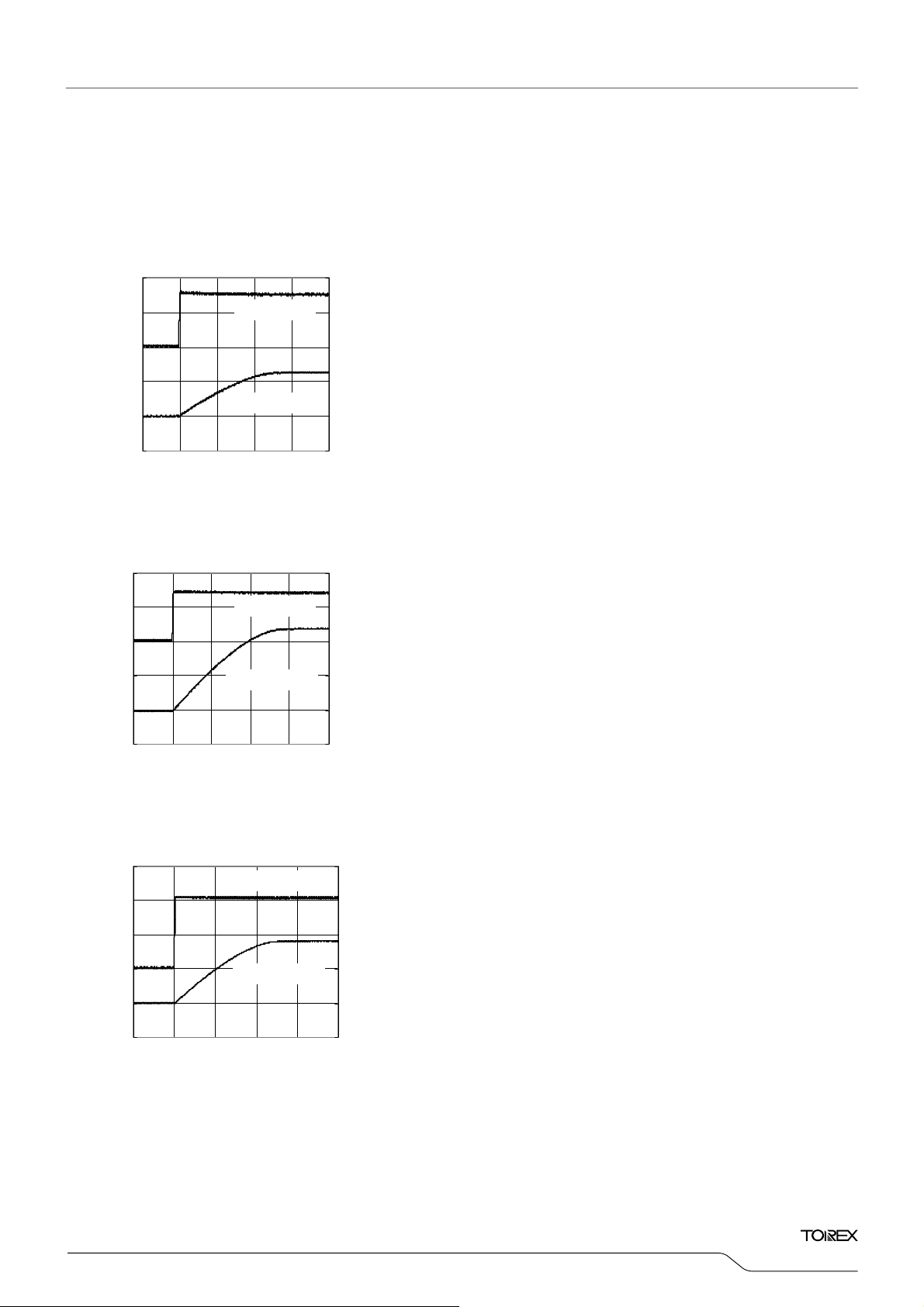
A
A
■TYPICAL PERFORMANCE CHARACTERISTICS (Continued)
* Unless otherwise stated, V
(16) Rising Response Time
BIAS=VCE
=3.6V, VIN=V
OUT(T)
+0.3V, I
OUT
=1mA , I
Pin=VSS, C
LIM
=1.0μF, CL=2.2μF, Ta = 25 ℃
BIAS=CIN
XC6604
Series
1
XC6604A051xR-G
V
=0V→0.8V(tr=5μs), I
IN
CIN=OPEN
=100mA
OUT
1.6
0.5
(V)
IN
0
-0.5
Input Voltage: V
-1
-1.5
Time (200μs/div)
Input Voltage
Output Voltage
1.2
0.8
0.4
0
-0.4
(V)
OUT
Output Voltage: V
XC6604A121xR-G
V
=0V→1.5V(tr=5μ), I
IN
2
1
(V)
IN
0
Input Voltage
CIN=OPEN
=100m
OUT
2
1.5
1
(V)
OUT
CIN=OPEN
=100m
OUT
0.5
0
-0.5
4
3
2
1
0
-1
Output Voltage: V
(V)
OUT
Output Voltage: V
-1
Input Voltage: V
-2
Output Voltage
-3
3
2
(V)
IN
1
0
Input Voltage: V
-1
-2
Time (200μs/div)
XC6604A181xR-G
V
=0V→2.1V(tr=5μs), I
IN
Input Voltage
Output Voltage
Time (200μs/div)
23/30
Page 24
A
A
A
XC6604 Series
■TYPICAL PERFORMANCE CHARACTERISTICS (Continued)
* Unless otherwise stated, V
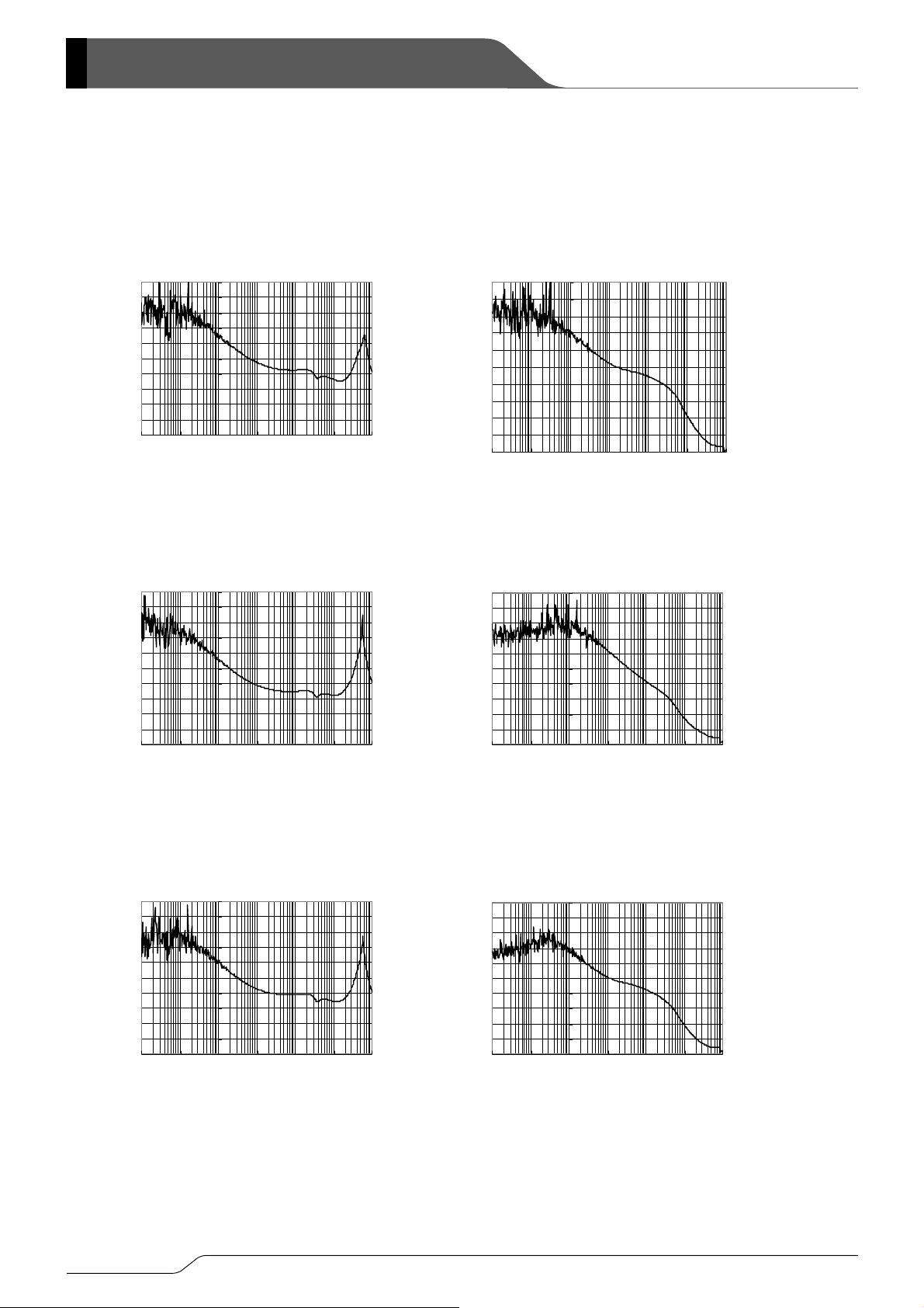
(17) Bias Voltage Ripple Rejection Rate (18) Input Voltage Ripple Rejection Rate
XC6604x051xR-G
100
90
80
70
(dB)
60
50
40
BIAS _PSRR
V
30
20
10
0
0.01 0.1 1 10 100 1000 10000
Frequency (kHz)
XC6604x121xR-G
100
90
80
70
(dB)
60
50
40
BIAS_ PSRR
V
30
20
10
0
0.01 0.1 1 10 100 1000 10000
Frequency (kHz)
XC6604x181xR-G
100
90
80
70
(dB)
60
50
40
BIAS_ PSRR
V
30
20
10
0
0.01 0.1 1 10 100 1000 10000
Frequency (kHz)
BIAS=VCE
V
V
V
=3.6V, VIN=V
=3.6VDC+0.2Vp-p
BIAS
=3.6VDC+0.2Vp-pAC, I
BIAS
=3.6VDC+0.2Vp-pAC, I
BIAS
OUT(T)
C
AC, IOUT
C
C
BIAS
BIAS
OUT
BIAS
OUT
=OPEN
=100m
=OPEN
=100m
=OPEN
=100m
+0.3V, I
OUT
=1mA , I
(dB)
IN _PSRR
V
(dB)
IN _PSRR
V
(dB)
IN _PSRR
V
Pin=VSS, C
LIM
=1.0μF, CL=2.2μF, Ta = 25 ℃
BIAS=CIN
XC6604x051xR-G
V
=0.8VDC+0.2Vp-pAC, I
IN
100
90
80
70
60
50
40
30
20
10
0
0.01 0.1 1 10 100 1000 10000
Frequency (kHz)
XC6604x121xR-G
=1.5VDC+0.2Vp-pAC, I
V
IN
100
90
80
70
60
50
40
30
20
10
0
0.01 0.1 1 10 100 1000 10000
Frequency (kHz)
XC6604x181xR-G
=2.1VDC+0.2Vp-pAC, I
V
IN
100
90
80
70
60
50
40
30
20
10
0
0.01 0.1 1 10 100 1000 10000
Frequency (kHz)
CIN=OPEN
=100mA
OUT
CIN=OPEN
=100mA
OUT
CIN=OPEN
=100mA
OUT
24/30
Page 25
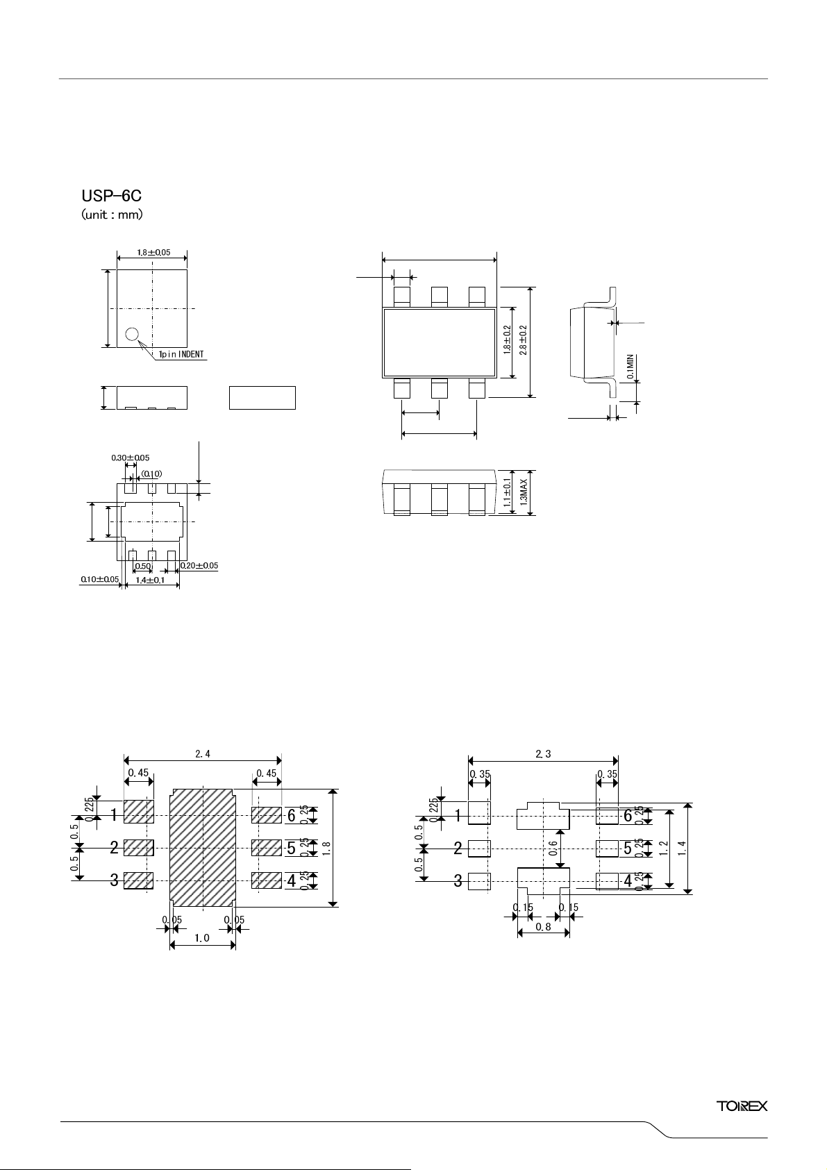
■PACKAGING INFORMATION
2.0±0.05
0.6MAX
0.25±0.05
1.0±0.1
0.70±0.05
●USP-6C Reference Pattern Layout (unit: mm) ●USP-6C Reference Metal Mask Design (unit: mm)
SOT-26W
(unit : mm)
+0.1
0.4
-0.05
6
1
(0.95)
2.9±0.2
5
2
1.9±0.2
4
0~0.1
3
+0.1
0.15
-0.05
XC6604
Series
25/30
Page 26
XC6604 Series
■PACKAGING INFORMATION (Continued)
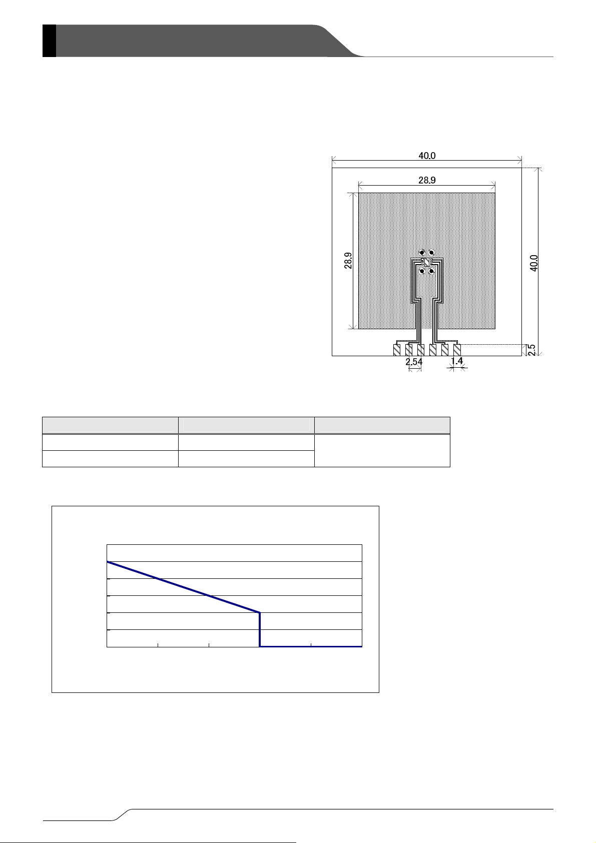
● USP-6C Power Dissipation
Power dissipation data for the USP-6C is shown in this page.
The value of power dissipation varies with the mount board conditions.
Please use this data as one of reference data taken in the described condition.
1. Measurement Condition (Reference data)
Condition: Mount on a board
Ambient: Natural convection
Soldering: Lead (Pb) free
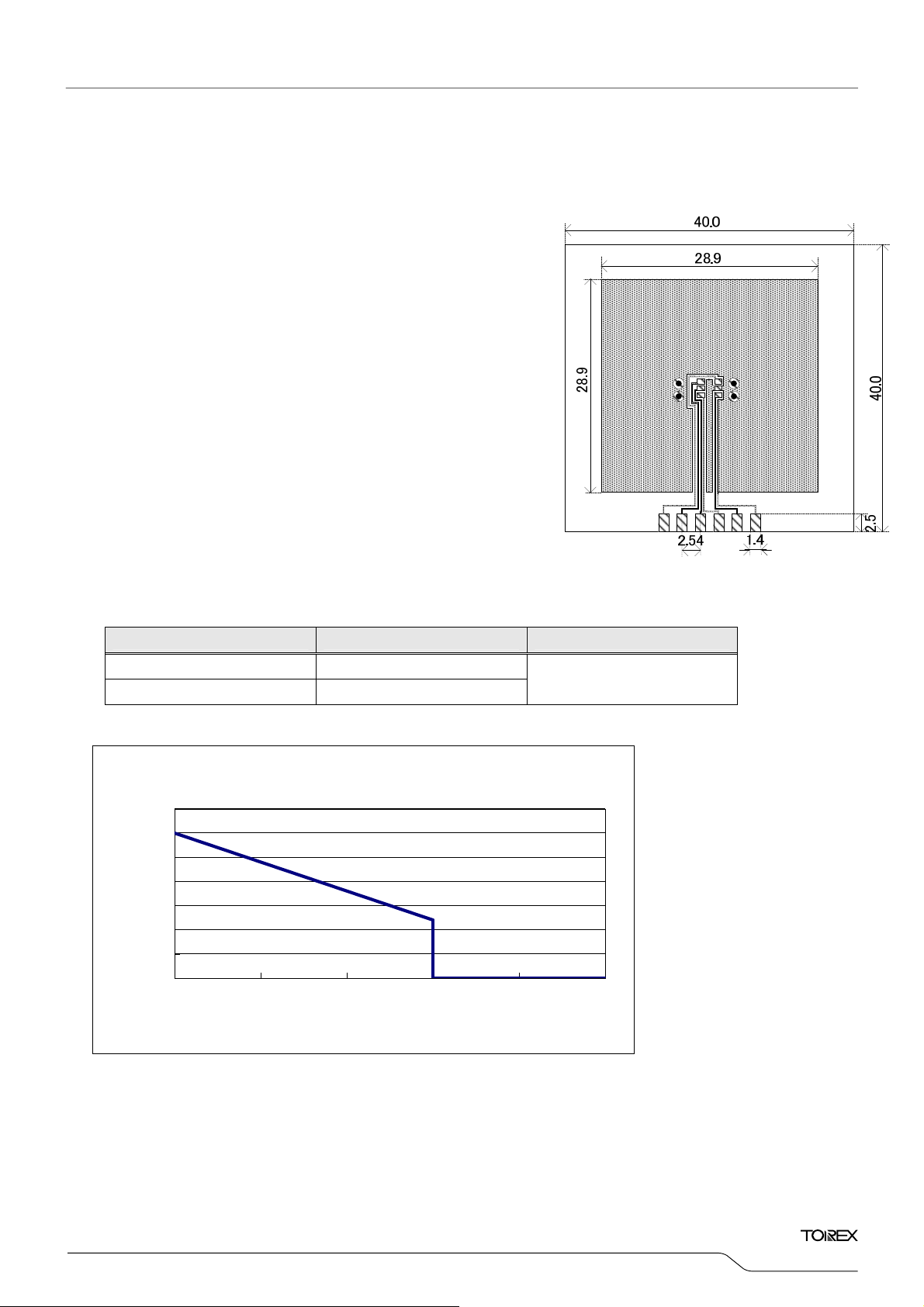
Board: Dimensions 40 x 40 mm (1600 mm
Copper (Cu) traces occupy 50% of the board area
Material: Glass Epoxy (FR-4)
Thickness: 1.6 mm
Through-hole: 4 x 0.8 Diameter
2. Power Dissipation vs. Ambient temperature
Board Mount (Tj max = 125℃)
In top and back faces
Package heat-sink is tied to the copper traces
Ambient Temperature (℃) Power Dissipation Pd (mW) Thermal Resistance (℃/W)
2
in one side)
Evaluation Board (Unit: mm)
Power Dissipation: Pd (mW)
26/30
25 1000
85 400
Pd-Ta特性
グラフ
Pd vs. Ta
1200
1000
800
600
400
200
許容損失Pd(mW)
0
25 45 65 85 105 125
Ambient Temperature: Ta (℃)
周辺温度
Ta(℃)
100.00
Page 27
p
(
)
XC6604
Series
■PACKAGING INFORMATION (Continued)
● SOT-26W Power Dissipation
Power dissipation data for the SOT-26W is shown in this page.
The value of power dissipation varies with the mount board conditions.
Please use this data as one of reference data taken in the described condition.
1. Measurement Condition (Reference data)
Condition: Mount on a board
Ambient: Natural convection
Soldering: Lead (Pb) free
Board: Dimensions 40 x 40 mm (1600 mm
Copper (Cu) traces occupy 50% of the board area
Material: Glass Epoxy (FR-4)
Thickness: 1.6 mm
Through-hole: 4 x 0.8 Diameter
2. Power Dissipation vs. Ambient temperature
Board Mount (Tj max = 125℃)
Ambient Temperature (℃) Power Dissipation Pd (mW) Thermal Resistance (℃/W)
In top and back faces
Package heat-sink is tied to the copper traces
(Board of SOT-26 is used.)
2
in one side)
評価基板レイアウト(単位:mm)
Evaluation Board (Unit: mm)
25 600
85 240
Pd-Ta特性グラフ
Pd vs. Ta
700
mW
600
166.67
500
400
ation: Pd
300
200
100
許容損失Pd(mW)
Power Dissi
0
25 45 65 85 105 125
Ambient Temperature: Ta (℃)
周辺温度Ta(℃)
27/30
Page 28
XC6604 Series
■MARKING RULE
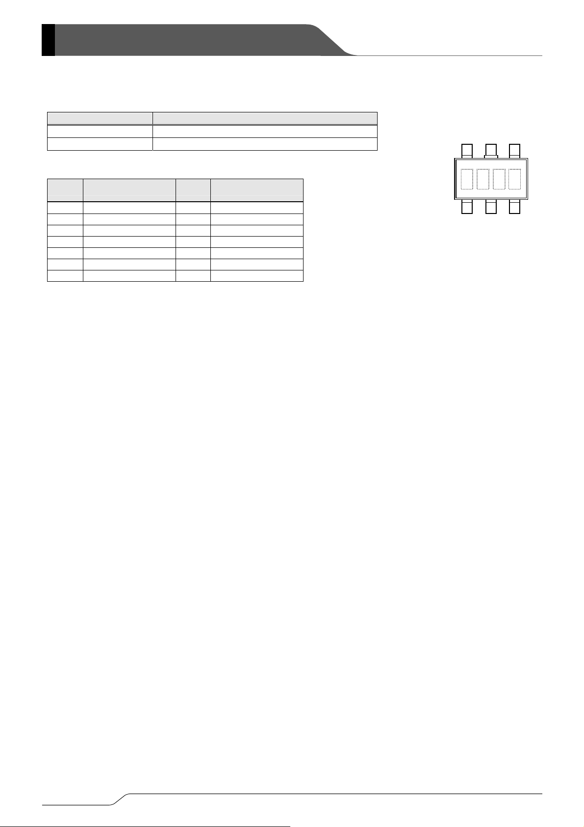
① represents product series
MARK PRODUCT SERIES
T XC6604A*****-G
U XC6604B*****-G
② represents output voltage
MARK OUTPUT VOLTAGE (V) MARK OUTPUT VOLTAGE (V)
A 0.5 K 1.2
B 0.6 L 1.3
C 0.7 M 1.4
D 0.8 N 1.5
E 0.9 P 1.6
F 1.0 R 1.7
H 1.1 S 1.8
③④ represents production lot number
01 to 09, 0A to 0Z, 11 to 9Z, A1 to A9, AA to Z9, B1 to ZZ in order.
(G, I, J, O, Q, W excluded)
*No character inversion used.
SOT-26W
64
5
① ② ③ ④
123
28/30
Page 29
r
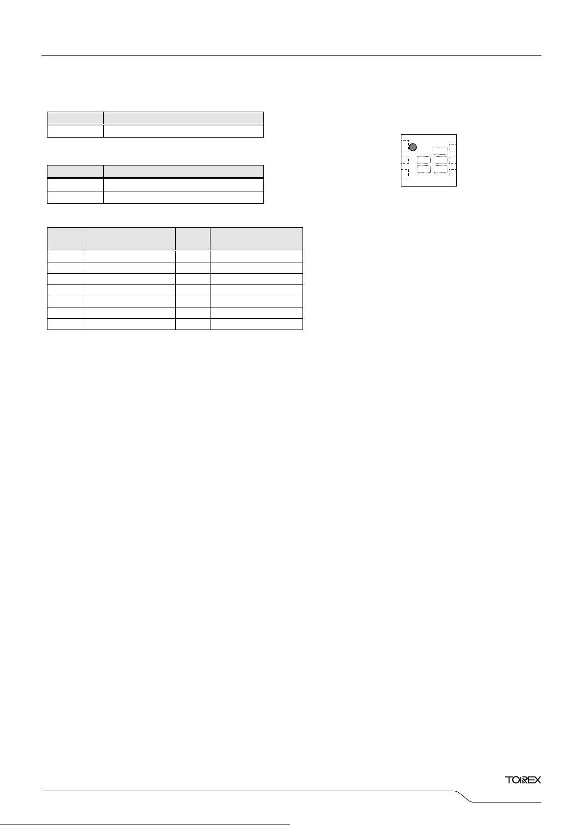
■MARKING RULE (Continued)
① represents product series
MARK PRODUCT SERIES
U XC6604******-G
② represents regulator type
MARK PRODUCT SERIES
A XC6604A*****-G
B XC6604B*****-G
③ represents output voltage
MARK OUTPUT VOLTAGE (V) MARK OUTPUT VOLTAGE (V)
A 0.5 K 1.2
B 0.6 L 1.3
C 0.7 M 1.4
D 0.8 N 1.5
E 0.9 P 1.6
F 1.0 R 1.7
H 1.1 S 1.8
④⑤ represents production lot numbe
01 to 09, 0A to 0Z, 11 to 9Z, A1 to A9, AA to Z9, B1 to ZZ in order.
(G, I, J, O, Q, W excluded)
*No character inversion used.
XC6604
Series
USP-6C
1
④ ⑤
2
3
6
② ③①
5
4
29/30
Page 30
XC6604 Series
1. The products and product specifications contained herein are subject to change without
notice to improve performance characteristics. Consult us, or our representatives
before use, to confirm that the information in this datasheet is up to date.
2. We assume no responsibility for any infringement of patents, patent rights, or other
rights arising from the use of any information and circuitry in this datasheet.
3. Please ensure suitable shipping controls (including fail-safe designs and aging
protection) are in force for equipment employing products listed in this datasheet.
4. The products in this datasheet are not developed, designed, or approved for use with
such equipment whose failure of malfunction can be reasonably expected to directly
endanger the life of, or cause significant injury to, the user.
(e.g. Atomic energy; aerospace; transport; combustion and associated safety
equipment thereof.)
5. Please use the products listed in this datasheet within the specified ranges.
Should you wish to use the products under conditions exceeding the specifications,
please consult us or our representatives.
6. We assume no responsibility for damage or loss due to abnormal use.
7. All rights reserved. No part of this datasheet may be copied or reproduced without the
prior permission of TOREX SEMICONDUCTOR LTD.
30/30
 Loading...