

Datasheet X9116WS8I, X9116WS8-2.7, X9116WS8, X9116WM8I-2.7, X9116WM8I Datasheet (XICOR)
...Page 1
A V A I L A B L E
AN99 • AN115 • AN120 • AN124 • AN133 • AN134
A
PPLICATION
N
OTE
Low Noise, Low Power, Low Cost
X9116
Digitally Controlled Potentiometer (XDCP
FEATURES
• Solid-state nonvolatile
• 16 wiper taps
• 3-wire up/down serial interface
•V
= 2.7V and 5V
CC
• Active current < 50µA max.
• Standby current < 1µA max.
•R
• Packages: MSOP-8, SOIC
TOTAL
= 10K Ω
™
)
DESCRIPTION
The Xicor X9116 is a digitally controlled nonvolatile
potentiometer designed to be used in trimmer applications. The pot consists of 15 equal resistor segments
that connect to the wiper pin through programmable
CMOS switches. The tap position is programmed
through a 3-wire up/down serial port. The last position
of the wiper is stored in a nonvolatile memory location
which is recalled at the time of power up of the device.
The wiper moves through sequential tap positions with
inputs on the serial port. A falling edge on INC (bar)
causes the tap position to increment one position up or
down based on whether the U/D (bar) pin is held high
or low.
The X9116 can be used in many applications requiring
a variable resistance. In many cases it can replace a
mechanical trimmer and offers many advantages such
as temperature and time stability as well as the reliability of a solid state solution.
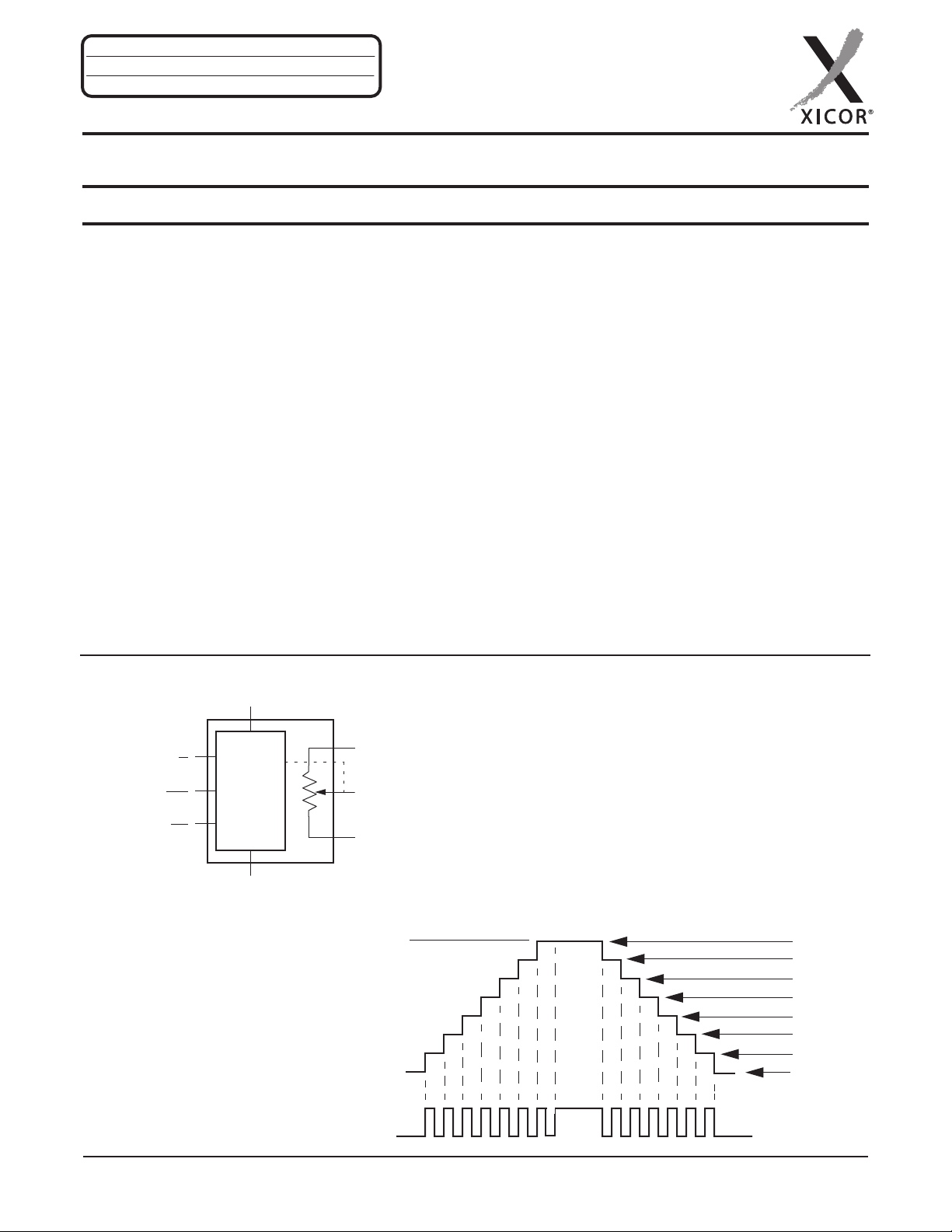
BLOCK DIAGRAM
V
CC
Up/Down
(U/D
)
Increment
(INC)
Device Select
(CS)
(Supply Voltage)
Control
and
Memory
V
(Ground)
SS
General
RH/V
RW/V
RL/V
R
H
W
L
RW-RL Resistance
R
H
*
3
2
1
0
L
15
14
13
10kΩ
9.34kΩ
8.68kΩ
* kΩ
2.08kΩ
1.42kΩ
760Ω
100Ω
REV 1.2 2/5/03
www.xicor.com
Characteristics subject to change without notice.
1 of 11
Page 2
X9116
.
.
PIN DESCRIPTIONS
V
/R
and V
H
H
The high (V
/R
L
L
/R
) and low (V
H
H
/R
) terminals of the
L
L
X9116 are equivalent to the fixed terminals of a
mechanical potentiometer. The minimum voltage is
V
and the maximum is V
SS
V
/R
W
W
R
/R
is the wiper terminal and is equivalent to the
w
w
CC
movable terminal of a mechanical potentiometer. The
position of the wiper within the array is determined by
the control inputs. The wiper terminal series resistance
is typically 200 Ω to 400 Ω depending upon V
CC
Up/Down (U/D)
The U/D input controls the direction of the wiper movement and whether the counter is incremented (up) or
decremented (down).
Increment (INC)
The INC input is negative-edge triggered. Toggling
INC will move the wiper and either increment or decrement the counter in the direction indicated by the logic
level on the U/D input.
Chip Select (CS)
The device is selected when the CS input is LOW. The
current counter value is stored in nonvolatile memory
when CS is returned HIGH while the INC input is also
HIGH. After the store operation is complete the X9116
will be placed in the low power standby mode until the
device is selected once again.
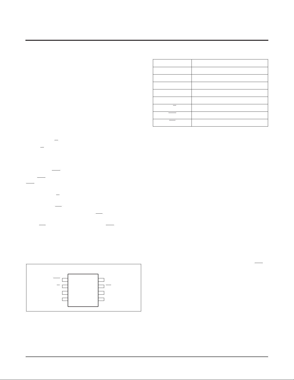
PIN CONFIGURATION
SOIC/MSOP
INC
U/D
VH/R
1
2
X9116
3
H
V
SS
4
V
8
CC
CS
7
VL/R
6
5
VW/R
L
W
PIN NAMES
Symbol Description
V
V
W
V
V
V
U/D
INC
H
L
CS
/R
/R
/R
SS
CC
H
W
L
High Terminal
Wiper Terminal
Low Terminal
Ground
Supply Voltage
Up/Down Control Input
Increment Control Input
Chip Select Input
PRINCIPLES OF OPERATION
There are three sections of the X9116: the input control, counter and decode section; the nonvolatile memory; and the resistor array. The input control section
operates just like an up/down counter. The output of
this counter is decoded to turn on a single electronic
switch connecting a point on the resistor array to the
wiper output. Under the proper conditions the contents
of the counter can be stored in nonvolatile memory
and retained for future use. The resistor array is comprised of 15 individual resistors connected in series. At
either end of the array and between each resistor is an
electronic switch that transfers the potential at that
point to the wiper pin.
The wiper, when at either fixed terminal, acts like its
mechanical equivalent and does not move beyond the
last position. That is, the counter does not wrap
around when clocked to either extreme.
The electronic switches on the device operate in a
“make before break” mode when the wiper changes
tap positions. If the wiper is moved several positions,
multiple taps are connected to the wiper for t
V
change). The R
W
value for the device can tem-
TOTAL
(INC to
IW
porarily be reduced by a significant amount if the wiper
is moved several positions.
When the device is powered-down, the last wiper position stored will be maintained in the nonvolatile memory. When power is restored, the contents of the
memory are recalled and the wiper is set to the value
last stored.
REV 1.2 2/5/03
www.xicor.com
Characteristics subject to change without notice.
2 of 11
Page 3
X9116
INSTRUCTIONS AND PROGRAMMING
The INC, U/D and CS inputs control the movement of
the wiper along the resistor array. With CS set LOW,
the device is selected and enabled to respond to the
U/D and INC inputs. HIGH to LOW transitions on INC
will increment or decrement (depending on the state of
the U/D input) a four bit counter. The output of this
counter is decoded to select one of 16 wiper positions
along the resistive array.
The value of the counter is stored in nonvolatile memory whenever CS transitions HIGH while the INC input
is also HIGH.
The system may select the X9116, move the wiper,
and deselect the device without having to store the latest wiper position in nonvolatile memory. After the
wiper movement is performed as described above and
once the new position is reached, the system must
keep INC
LOW while taking CS HIGH. The new wiper
position will be maintained until changed by the system or until a power-up/down cycle recalls the previously stored data.
This procedure allows the system to always power-up
to a preset value stored in nonvolatile memory; then
during system operation, minor adjustments could be
made. The adjustments might be based on user preference, system parameter changes due to temperature drift, etc.
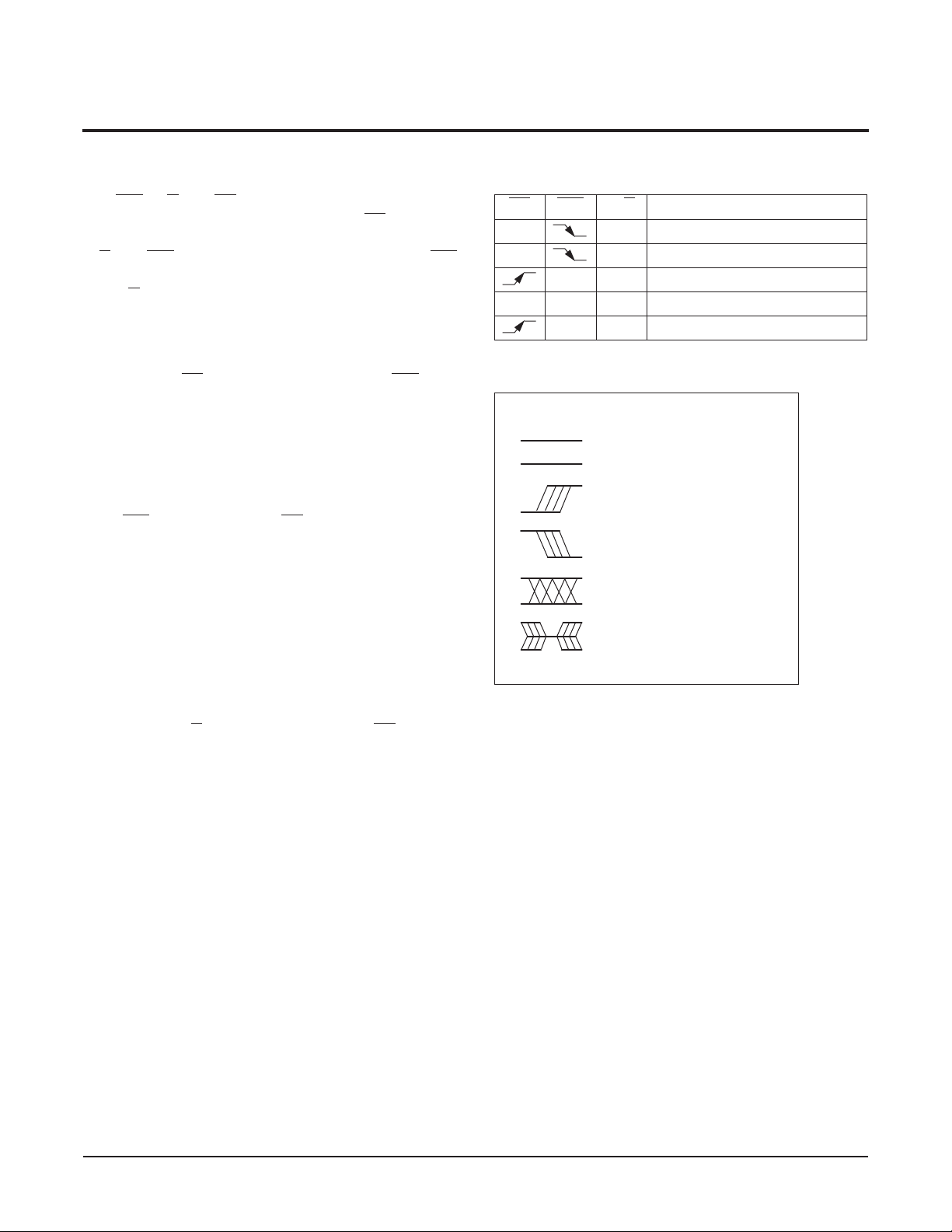
MODE SELECTION
CS INC U/D Mode
L H Wiper Up
L L Wiper Down
H X Store Wiper Position
H X X Standby Current
L X No Store, Return to Standby
SYMBOL TABLE
WAVEFORM INPUTS OUTPUTS
Must be
steady
May change
from Low to
High
May change
from High to
Low
Don’t Care:
Changes
Allowed
N/A Center Line
Will be
steady
Will change
from Low to
High
Will change
from High to
Low
Changing:
State Not
Known
is High
Impedance
The state of U/D may be changed while CS remains
LOW. This allows the host system to enable the device
and then move the wiper up and down until the proper
trim is attained.
REV 1.2 2/5/03
www.xicor.com
Characteristics subject to change without notice.
3 of 11
Page 4
X9116
∆
=
ABSOLUTE MAXIMUM RATINGS
Temperature under bias ....................–65 ° C to +135 ° C
Storage temperature .........................–65°C to +150°C
Voltage on CS, INC, U/D, V
and V
V = |V
with respect to V
CC
/R
–V
H
/R
H
L
| ............................................ 5.5V
L
/R
, V
/R
H
H
...................–1V to +7V
SS
L
L
Lead temperature (soldering 10 seconds)..........300°C
I
(10 seconds) ............................................ ±10.0mA
W
COMMENT
Stresses above those listed under “Absolute Maximum
Ratings” may cause permanent damage to the device.
This is a stress rating only; the functional operation of
the device (at these or any other conditions above
those listed in the operational sections of this specification) is not implied. Exposure to absolute maximum
rating conditions for extended periods may affect
device reliability.
RECOMMENDED OPERATING CONDITIONS
Temperature Min. Max.
Commercial 0°C +70°C
Industrial –40°C +85°C
Supply Voltage (V
) Limits
CC
X9116 5V ±10%
X9116-2.7 2.7V to 5.5V
POTENTIOMETER CHARACTERISTICS (Over recommended operating conditions unless otherwise stated)
Limits
Symbol Parameter
R
TOTAL
V
V
VH
VL
End to end resistance variation –20 +20 %
V
/R
terminal voltage V
H
H
VL/RL terminal voltage V
Power rating 10 mW R
R
W
R
W
I
W
Wiper resistance 200 400 Ω IW = 1mA, VCC = 5V
Wiper resistance 400 1000 Ω IW = 1mA, VCC = 2.7V
Wiper current -5.0 +5.0 mA
SS
SS
V
CC
V
CC
VV
VVSS = 0V
Test Conditions/NotesMin. Typ. Max. Unit
0V
SS
TOTAL
= 10 KΩ
Noise -120 dBV√Hz Ref: 1kHz
Resolution 6 %
Absolute linearity
Relative linearity
R
temperature coefficient ±300 ppm/°C
TOTAL
(2)
(1)
-1 +1 MI
-0.2 +0.2 MI
(3)
(3)
V
w(n)(actual)–Vw(n)(expected)
V
w(n+1)
–[V
w(n)+MI
]
Ratiometric temperature coefficient ±20 ppm/°C
C
H/CL/CW
Potentiometer capacitances 10/10/25 pF See Circuit #3
Notes: (1) Absolute linearity is utilized to determine actual wiper voltage versus expected voltage = (V
Ml Maximum.
(2) Relative linearity is a measure of the error in step size between taps = V
(3) 1 Ml = Minimum Increment = R
REV 1.2 2/5/03
TOT
/15.
www.xicor.com
W(n+1)
–[V
+ Ml] = ±0.2 Ml.
w(n)
Characteristics subject to change without notice.
(actual)–V
w(n)
(expected)) = ±1
w(n)
4 of 11
Page 5

X9116
C
H
C
L
R
W
10pF
10pF
R
H
R
L
R
TOTAL
C
W
25pF
D.C. OPERATING CHARACTERISTICS (Over recommended operating conditions unless otherwise specified)
Limits
Symbol Parameter
I
CC1
I
CC2
VCC active current (Increment) 150 µA CS = VIL, U/D = VIL or VIH and
VCC active current (Store)
(EEPROM Store)
I
SB
I
LI
Standby supply current 1 µA CS = VCC–0.3V, U/D and
CS, INC, U/D input leakage
current
V
IH
V
IL
C
IN
Notes: (4) Typical values are for TA = 25°C and nominal supply voltage.
CS, INC, U/D input HIGH voltage 2V VCC + 0.5 V
CS, INC, U/D input LOW voltage –0.5 0.8 V
(5)
CS, INC, U/D input capacitance 10 pF VCC = 5V, VIN = VSS,
(5) This parameter is periodically sampled and not 100% tested.
ENDURANCE AND DATA RETENTION
(4)
Max.
Unit Test ConditionsMin. Typ.
= 0.4V/2.4V @ max. t
INC
CYC
400 µA CS = VIH, U/D = VIL or VIH and
= V
INC
INC
±10 µA VIN = V
= 25°C, f = 1MHz
T
A
@ max. t
IH
WR
= VSS or VCC–0.3V
to V
SS
CC
Parameter Min. Unit
Minimum endurance 100,000 Data changes per bit
Data retention 100 Years
Test Circuit #1
VH/R
H
V
S
VL/R
VW/R
L
Test Point
W
A.C. CONDITIONS OF TEST
Input pulse levels 0V to 3V
Input rise and fall times 10ns
Input reference levels 1.5V
Test Circuit #2
VH/R
H
VW/R
V
VL/R
L
L
VW
Test Point
W
Force
Current
Circuit #3 SPICE Macro Model
REV 1.2 2/5/03
www.xicor.com
Characteristics subject to change without notice. 5 of 11
Page 6

X9116
A.C. OPERATING CHARACTERISTICS (Over recommended operating conditions unless otherwise specified)
Limits
Symbol Parameter
t
t
t
t
t
t
t
CPH
t
IW
t
CYC
t
,
R
t
PU
t
R VCC
t
WR
Cl
lD
DI
lL
lH
lC
t
F
(7)
(7)
(7)
CS to INC setup 100 ns
INC HIGH to U/D change 100 ns
U/D to INC setup 2.9 µs
INC LOW period 1 µs
INC HIGH period 1 µs
INC inactive to CS inactive 1 µs
CS deselect time (STORE) 10 ms
INC to Vw change 1 5 µs
INC cycle time 4 µs
INC input rise and fall time 500 µs
Power up to wiper stable 5 µs
VCC Power-up rate 15 50 mV/µs
Store cycle 5 10 ms
(6)
Max.
UnitMin. Typ.
POWER UP AND DOWN REQUIREMENTS
There are no restrictions on the power-up or power-down conditions of VCC and the voltages applied to the potentiometer pins provided that VCC is always more positive than or equal to VH, VL, and VW, i.e., VCC ≥ VH, VL, VW. The
VCC ramp rate spec is always in effect.
A.C. TIMING
CS
t
INC
U/D
V
CYC
t
CI
t
IW
W
t
IL
t
ID
t
IH
t
DI
(store)
t
IC
(8)
MI
t
CPH
t
F
90% 90%
10%
t
R
Notes: (6) Typical values are for TA = 25°C and nominal supply voltage.
(7) This parameter is not 100% tested.
(8) MI in the A.C. timing diagram refers to the minimum incremental change in the VW output due to a change in the wiper position.
REV 1.2 2/5/03
www.xicor.com
Characteristics subject to change without notice. 6 of 11
Page 7

X9116
Basic Configurations of Electronic Potentiometers
V
R
V
H
V
L
VW/R
W
V
R
I
Basic Circuits
R
V
1
REF
+V
Three terminal potentiometer;
variable voltage divider
+5V
V
W
OP-07
+
–
V
OUT
–5V
= VW/R
V
OUT
W
Voltage Regulator
Cascading TechniquesBuffered Reference Voltage
+V +V
VW/R
W
+V
(a) (b)
Two terminal variable resistor;
variable current
Noninverting Amplifier
V
S
X
V
W
VO = (1+R2/R1)V
Comparator with Hysteresis
+5V
LM308A
+
–
V
O
–5V
R
2
R
1
S
REV 1.2 2/5/03
IN
317
R
I
adj
R
2
VO (REG) = 1.25V (1+R2/R1)+Iadj R
VO (REG)V
1
LT311A
V
S
–
+
}
}
R
R
V
= {R1/(R1+R2)} VO(max)
UL
2
1
V
O
VLL = {R1/(R1+R2)} VO(min)
2
(for additional circuits see AN115)
www.xicor.com
Characteristics subject to change without notice. 7 of 11
Page 8

X9116
PACKAGING INFORMATION
8-Lead Miniature Small Outline Gull Wing Package Type M
0.012 + 0.006 / -0.002
(0.30 + 0.15 / -0.05)
0.118 ± 0.002
(3.00 ± 0.05)
0.030 (0.76)
0.118 ± 0.002
(3.00 ± 0.05)
0.0256 (0.65) Typ.
R 0.014 (0.36)
0.007 (0.18)
0.005 (0.13)
0.036 (0.91)
0.032 (0.81)
0.040 ± 0.002
(1.02 ± 0.05)
0.150 (3.81)
Ref.
0.193 (4.90)
Ref.
0.0216 (0.55)
7° Typ.
0.008 (0.20)
0.004 (0.10)
0.0256" Typical
0.025"
Typical
0.220"
0.020"
Typical
8 PlacesFOOTPRINT
REV 1.2 2/5/03
NOTE:
1. ALL DIMENSIONS IN INCHES AND (MILLIMETERS)
www.xicor.com
Characteristics subject to change without notice. 8 of 11
Page 9

X9116
PACKAGING INFORMATION
8-Lead Miniature Small Outline Gull Wing Package Type M
0.012 + 0.006 / -0.002
(0.30 + 0.15 / -0.05)
0.118 ± 0.002
(3.00 ± 0.05)
0.030 (0.76)
0.118 ± 0.002
(3.00 ± 0.05)
0.0256 (0.65) Typ.
R 0.014 (0.36)
0.007 (0.18)
0.005 (0.13)
0.036 (0.91)
0.032 (0.81)
0.040 ± 0.002
(1.02 ± 0.05)
0.150 (3.81)
Ref.
0.193 (4.90)
Ref.
0.0216 (0.55)
7° Typ.
0.008 (0.20)
0.004 (0.10)
0.0256" Typical
0.025"
Typical
0.220"
0.020"
Typical
8 PlacesFOOTPRINT
REV 1.2 2/5/03
NOTE:
1. ALL DIMENSIONS IN INCHES AND (MILLIMETERS)
www.xicor.com
Characteristics subject to change without notice. 9 of 11
Page 10

X9116
PACKAGING INFORMATION
8-Lead Plastic Small Outline Gull Wing Package Type S
Pin 1 Index
(4X) 7°
0.050 (1.27)
0.010 (0.25)
0.020 (0.50)
Pin 1
X 45°
0.014 (0.35)
0.019 (0.49)
0.188 (4.78)
0.197 (5.00)
0.150 (3.80)
0.158 (4.00)
0.004 (0.19)
0.010 (0.25)
0.228 (5.80)
0.244 (6.20)
0.053 (1.35)
0.069 (1.75)
0.050"Typical
0° - 8°
REV 1.2 2/5/03
0.0075 (0.19)
0.010 (0.25)
0.016 (0.410)
0.037 (0.937)
NOTE: ALL DIMENSIONS IN INCHES (IN PARENTHESES IN MILLIMETERS)
www.xicor.com
0.250"
Characteristics subject to change without notice. 10 of 11
0.050"
Typical
0.030"
Typical
8 PlacesFOOTPRINT
Page 11

X9116
Ordering Information
X9116X X X X
VCC Limits
Blank = 5V ±10%
–2.7 = 2.7V to 5.5V
Temperature Range
Blank = Commercial = 0°C to +70°C
I = Industrial = –40°C to +85°C
Package
M8 = 8-Lead MSOP
S8 = 8-Lead SOIC
End to End Resistance
W = 10KΩ
LIMITED WARRANTY
Devices sold by Xicor, Inc. are covered by the warranty and patent indemnification provisions appearing in its Terms of Sale only. Xicor, Inc. makes no warranty,
express, statutory, implied, or by description regarding the information set forth herein or regarding the freedom of the described devices from patent infringement.
Xicor, Inc. makes no warranty of merchantability or fitness for any purpose. Xicor, Inc. reserves the right to discontinue production and change specifications and prices
at any time and without notice.
Xicor, Inc. assumes no responsibility for the use of any circuitry other than circuitry embodied in a Xicor, Inc. product. No other circuits, patents, or licenses are implied.
TRADEMARK DISCLAIMER:
Xicor and the Xicor logo are registered trademarks of Xicor, Inc. AutoStore, Direct Write, Block Lock, SerialFlash, MPS, and XDCP are also trademarks of Xicor, Inc. All
others belong to their respective owners.
U.S. PATENTS
Xicor products are covered by one or more of the following U.S. Patents: 4,326,134; 4,393,481; 4,404,475; 4,450,402; 4,486,769; 4,488,060; 4,520,461; 4,533,846;
4,599,706; 4,617,652; 4,668,932; 4,752,912; 4,829,482; 4,874,967; 4,883,976; 4,980,859; 5,012,132; 5,003,197; 5,023,694; 5,084,667; 5,153,880; 5,153,691;
5,161,137; 5,219,774; 5,270,927; 5,324,676; 5,434,396; 5,544,103; 5,587,573; 5,835,409; 5,977,585. Foreign patents and additional patents pending.
LIFE RELATED POLICY
In situations where semiconductor component failure may endanger life, system designers using this product should design the system with appropriate error detection
and correction, redundancy and back-up features to prevent such an occurrence.
Xicor’s products are not authorized for use in critical components in life support devices or systems.
1. Life support devices or systems are devices or systems which, (a) are intended for surgical implant into the body, or (b) support or sustain life, and whose failure to
perform, when properly used in accordance with instructions for use provided in the labeling, can be reasonably expected to result in a significant injury to the user.
2. A critical component is any component of a life support device or system whose failure to perform can be reasonably expected to cause the failure of the life
support device or system, or to affect its safety or effectiveness.
REV 1.2 2/5/03
www.xicor.com
Characteristics subject to change without notice. 11 of 11
©Xicor, Inc. 2000 Patents Pending
 Loading...