

Datasheet X88C75JISLIC, X88C75PSLIC, X88C75PMSLIC, X88C75PISLIC, X88C75LSLIC Datasheet (XICOR)
...Page 1
X88C75 SLIC® E
2
1
Port Expander and E2 Memory
FEATURES
• Highly Integrated Microcontroller Peripheral
—8K x 8 E2 Memory
—2 x 8 General Purpose Bidirectional I/O Ports
—16 x 8 General Purpose Registers
—Integerated Interrupt Controller Module
—Internal Programmable Address Decoding
• Self Loading Integrated Code (SLIC)
—On-Chip BIOS and Boot Loader
—IBM/PC Based Interface Software(XSLIC)
• Concurrent Read During Write
—Dual Plane Architecture
• Isolates Read/Write Functions Between Planes
• Allows Continuous Execution Of Code From
One Plane While Writing In The Other Plane
• Multiplexed Address/Data Bus
—Direct Interface to Popular 80C51 Family of
Microcontrollers
• Software Data Protection
—Protect Entire Array During Power-up/-down
• Block Lock™ Data Protection
—Set Write Lockout in 1K Blocks
• Toggle Bit Polling
• High Performance CMOS
—Fast Access Time, 120ns
—Low Power
• 60mA Active
• 100µA Standby
• PDIP, PLCC, and TQFP Packaging Available
DESCRIPTION
The X88C75 SLIC is a highly integrated peripheral for
the 80C51 family of microcontrollers. The device integrates 8K-bytes of 5V byte-alterable nonvolatile memory,
two bidirectional 8-bit ports, 16 general purpose registers, programmable internal address decoding and a
multiplexed address and data bus.
The 5V byte-alterable nonvolatile memory can be used
as program storage, data storage, or a combination of
both. The memory array is separated into two 4K-bytes
sections which allows read accesses to one section
while a write operation is taking place in the other
section. The nonvolatile memory also features Software
Data Protection to protect the contents during power
transitions, and an advanced Block Protect register
©Xicor, Inc. 1994, 1995, 1996 Patents Pending Characteristics subject to change without notice
2887-2.5 4/11/97 T0/C0/D1 SH
SLIC
2887 ILL F01
RESET
A
12
WC
PSEN
STRA
A
15
NC
A
14
A
13
PA
7
PA
6
PA
5
PA
4
PA
3
PA
2
PA
1
PA
0
NC
A/D
0
A/D
1
A/D
2
A/D
3
A/D
4
V
SS
1
2
3
4
5
6
7
8
9
10
11
12
13
14
15
16
17
18
19
20
21
22
23
24
48
47
46
45
44
43
42
41
40
39
38
37
36
35
34
33
32
31
30
29
28
27
26
25
V
CC
WR
ALE
A
8
A
9
A
11
NC
IRQ
STRB
PB
7
PB
6
PB
5
PB
4
PB
3
PB
2
PB
1
PB
0
NC
RD
A
10
CE
A/D
7
A/D
6
A/D
5
X88C75
PIN CONFIGURATIONS
DIP
2887 ILL F01
X88C75 SLIC® E2 Microperipheral
Concurrent Read During Write, Block Lock, and
SLIC
®
E2 are registered trademarks of Xicor, Inc.
APPLICATION NOTES
AVAILABLE
AN62 • AN64 • AN66
INDEX
CORNER
2887 ILL F02.4
6 5 4 3 2 1 44 43 42 41 40
18 19 20
22 23
24 25 26 27 28
21
39
38
37
36
35
34
33
32
31
30
29
7
8
9
10
11
12
13
14
15
16
17
A
15
STRA
PSEN
WC
A
12
RESET
V
CC
WR
ALE
A
8
A
9
A
11
IRQ
STRB
PB
7
PB
6
PB
5
PB
4
PB
3
PB
2
PB
1
PB
0
A
14
A
13
PA
7
PA
6
PA
5
PA
4
4
PA
3
33
PA
2
PA
1
PA
0
A/D
0
A/D
1
A/D
2
A/D
3
A/D
4
V
SS
A/D
5
A/D
6
A/D
7
CE
A
10
RD
X88C75
SLIC
PLCC
TQFP
Page 2
X88C75 SLIC® E
2
2
Reading and writing of the nonvolatile memory array is
analogous to RAM operation. During a write operation to
either the nonvolatile memory or the control registers,
ALE latches the address to be written into the X88C75.
The rising edge of WR latches the data to be written.
The nonvolatile memory of the X88C75 is internally
organized as two independent arrays of 4K-bytes with
the A12 input selecting which of the two planes of
memory is to be accessed. While the processor is
executing code out of one plane, write operations can
take place in the other plane; allowing the processor to
continue execution of code out of the X88C75 during a
byte or page write to the device. This feature is called
Concurrent Read During Write.
The X88C75 also features an advanced implementation
of the Software Data Protection scheme, called Block
Lock Protect, which allows the nonvolatile memory array
to be treated as 8 independent sections of 1K-bytes.
Each of these sections can be independently enabled
for write operations. This allows segmentation of the
memory contents into writable and non-writable sections, thereby, allowing certain sections of the device to
be secured so that updates can only occur in a controlled
environment. (e.g. in an automotive application, only at
which allows Individual blocks of the memory to be
configured as read-only or read/write.
Each bidirectional port consists of 8 general purpose
I/O lines and 1 data strobe line. The ports also feature a
configurable interrupt request output.
Access to the X88C75 is accomplished through the
multiplexed address/data bus of the 80C51 type controllers. An internal programmable address decoder maps
the internal memory and register locations into the
desired address space.
ARCHITECTURAL OVERVIEW
The X88C75 incorporates the interface circuitry normally needed to decode the control signals and
demultiplex the address/data bus to provide a “seamless” interface.
The control inputs on the X88C75 are configured such
that it is possible to directly connect them to the proper
interface signals of the 80C51 microcontroller. The
reading of data from the chip is controlled either by the
PSEN or the RD signal, which essentially maps the
X88C75 into both the Program and the Data Memory
address map.
FUNCTIONAL DIAGRAM
2887 ILL F03
ADDRESS
LATCH
I/O
BUFFER
&
LATCH
MASTER
CONTROL
LOGIC
LEFT PLANE
DECODE
RIGHT PLANE
DECODE
1K X 8
1K X 8
E2PROM
CE
ALE
PSEN
RD
WR
RESET
IRQ
1K X 8
1K X 8
1K X 8
1K X 8
1K X 8
1K X 8
SDP
DECODE
CONFIG
REGISTER
MAPMEM.
PORT
SPECIAL
FUNCTION
REGISTERS
PORT
A
PORT
B
PORT SELECT
DAT A I/O BUS
A0–A
15
I/O0–I/O
7
WC
E2PROM
16 X 8
GENERAL
PURPOSE
REGISTERS
Page 3
X88C75 SLIC® E
2
3
an authorized service center). The Block Protect configuration is stored in a nonvolatile register, ensuring
that the configuration data will be maintained after the
device is powered-down.
The X88C75 write control input, serves as an external
control over the completion of a previously initiated page
load cycle.
The X88C75 also features the industry standard 5V E
2
memory characteristics such as byte or page mode write
and Toggle Bit Polling.
Read
A HIGH to LOW transition on ALE latches the address;
the data will be output on the AD pins after either RD or
PSEN goes LOW (t
RDLV
).
Write
A write is performed by latching the addresses on the
falling edge of ALE. The WR is strobed LOW followed by
valid data being presented on the AD0–AD7 pins. The
data will be latched into the X88C75 on the rising edge
of WR.
Page Write Operation
The X88C75 supports page mode write operations. This
allows the microcontroller to write from one to thirty-two
bytes of data to the X88C75. Each individual write within
a page write operation must conform to the byte write
timing requirements. The falling edge of WR starts a
timer delaying the internal programming cycle 100µs:
therefore, each successive write operation must begin
within 100µs of the last byte written. The waveform
on page 4 illustrates the sequence and timing
requirements.
PIN DESCRIPTIONS
PIN NAME I/O DESCRIPTION
RESET I RESET is used to initialize the internal static registers and has no effect on the E2 memory opera-
tions. The default active level is HIGH, but it can be reconfigured in EEM register.
PSEN I Content of E
2
memory can be read by lowering the PSEN and holding both RD and WR HIGH. The
device then places on the data bus (AD7–AD0) the contents of E2 memory at the latched address.
STRA, STRB I/O The STRA controls port A and STRB controls port B. When ports are configured as inputs, a valid
transition on their strobe pins will latch into their port data register the data present at the port input
pins. Writing to an output port data register generates a pulse of fixed duration on its corresponding
strobe pin. The output data presented at the output pins stay valid until the next data is written to the
output port data register.
PA
7
–PA
0
I/O The I/O lines of port A. The output driver can be configured as either CMOS or open-drain using the
AWO bit in CR. The I/O direction bit (DIRA) in CR is used to select port A I/O mode.
PB
7
–PB
0
I/O The I/O lines of port B. The output driver can be configured as either CMOS or open-drain using the
BWO bit in CR. The I/O direction bit (DIRB) in CR is used to select port B I/O mode.
A15–A
8
I Non-multiplexed high-order Address Bus inputs for the upper byte of the address.
AD
7
–AD
0
I/O Multiplexed low-order Address and Data Bus. The addresses are latched when ALE makes a HIGH
to LOW transition.
WR I During a byte/page write cycle WR is brought LOW while RD is held HIGH and the data is placed on
the Data Bus. The rising edge of WR will latch the data into the device.
RD I The RD input is active LOW and is used to read content of either the E
2
memory or the SFR at the
latched address. Both PSEN and WR signals must be held HIGH during RD controlled read
operation.
IRQ O The IRQ is an open-drain output. It can be configured to signal latching of new data into any of the
ports, and/or completion of the E2 memory internal write cycle.
WC I WC input has to be held LOW during a write cycle. It can be permanently tied HIGH in order to
disable write to the E
2
memory. Taking WC HIGH prior to t
BLC
(100µs, the time delay from the last
write cycle to the start of internal programming cycle) will inhibit the write operation.
CE I The device select (CE) is an active LOW input. This signal has to be asserted prior to ALE HIGH to
LOW transition in order to generate a valid internal device select signal. Holding this pin HIGH and
ALE LOW will place the device in standby mode. The ports stay active at all times.
ALE I Address Latch Enable input is used to latch the addresses present on the address lines A
15–A8
and
AD7–AD0 into the device. The addresses are latched when ALE transitions from HIGH to LOW.
2887 PGM T01.1
Page 4
X88C75 SLIC® E
2
4
Page Write Operation
Toggle Bit Polling
Because the X88C75 typical write timing is less than the
specified 5ms, Toggle Bit Polling has been provided to
determine the early completion of a write cycle. During
the internal programming cycle, I/O6 will toggle from “1”
to “0” and “0” to “1” on subsequent attempts to read from
the memory plane that is being updated. When the
Figure 1. Toggle Bit Polling
internal cycle is complete, the toggling will cease and
the device will be accessible for additional read or write
operations. Due to the dual plane architecture, reads for
polling must occur from the plane that was written; that
is, the state of A
12
during a write must match the state
of A12 during polling.
t
BLC
CE
ALE
A/D0–A/D
7
A8–A
12
WR
PSEN(RD)
A
IN
D
IN
A12=n
OPERATION
BYTE 0
BYTE 1
BYTE 2 LAST BYTE READ (1)(2) AFTER tWC READY FOR
NEXT WRITE OPERATION
t
WC
2887 ILL F04
A
IN
D
IN
A12=n
A
IN
D
IN
A12=n
A
IN
D
IN
A12=n
A
IN
D
OUT
A12=x
A
IN
ADDR
A
IN
Next Address
RD
LAST BYTE
WRITTEN
CE
ALE
A/D0–A/D
7
A8–A
12
WR
A
IN
D
IN
A12=n
OPERATION
A
IN
D
OUT
A12=n
A
IN
D
OUT
A12=n
A
IN
D
OUT
A12=n
A
IN
D
OUT
A12=x
A
IN
ADDR
I/O6=X
X88C75 READY FOR
NEXT OPERATION
2887 ILL F05
I/O6=X I/O6=X I/O6=X
Page 5
X88C75 SLIC® E
2
5
DATA PROTECTION
The X88C75 provides two levels of data protection
through software control. There is a global software data
protection feature similar to the industry standard for
E2PROMs and a new Block Lock Protect write lockout
protection providing a secondary level data security
option.
Software Data Protection
Software Data Protection (SDP) can be employed to
protect the entire array against inadvertent writes during
power-up/power-down operations. The X88C75 is
shipped from the factory with SDP enabled. With SDP
enabled, inadvertent attempts to write to the X88C75 will
be blocked.
The system can still write data, but only when the write
operation (page or byte) is preceded by the three-byte
command sequence. All write operations, both the command sequence and any data write operations must
conform to the page write timing requirements.
The SDP mode is also enabled anytime one of the
nonvolatile configuration registers are modified. These
include writing to EE map, SFR map, and BPR.
Block Lock Protect Write Lockout
The X88C75 provides a second level of data security
referred to as Block Lock Protect write lockout (or Block
Protect). This is accessed through an extension of the
SDP command sequence. Block Protect allows the user
to lockout writes to 1K x 8 blocks of memory. Unlike SDP
which prevents inadvertent writes, but still allows easy
system access to writing the memory, Block Protect will
lockout all attempts unless it is specifically disabled by
issuing the deactivation sequence. This feature can be
used to set a higher level of protection in a system where
a portion of the memory is used to store the system
kernel and protect it from the application programs
residing in the other blocks.
Setting write lockout is accomplished by writing a fivebyte command sequence opening access to the Block
Protect Register (BPR). After the fifth byte is written, the
user writes to the BPR, selecting which blocks to protect
or unprotect. All write operations, both the command
sequence and writing the data to the BPR, must conform
to the page write timing requirements. It should be noted
Figure 2. Writing With SDP Enabled
AA
b
2
P 555b1b
0
55
b
2
AAAb1b
0
A0
b
2
P 555b1b
0
2887 ILL F06
Perform Byte or
Page Write Operations
Reference the A15–A13
setting in EEM register
P = Address bit (A12) of the
updated memory plane
Delay of t
WC
Exit Routine
b2b1b
0
P
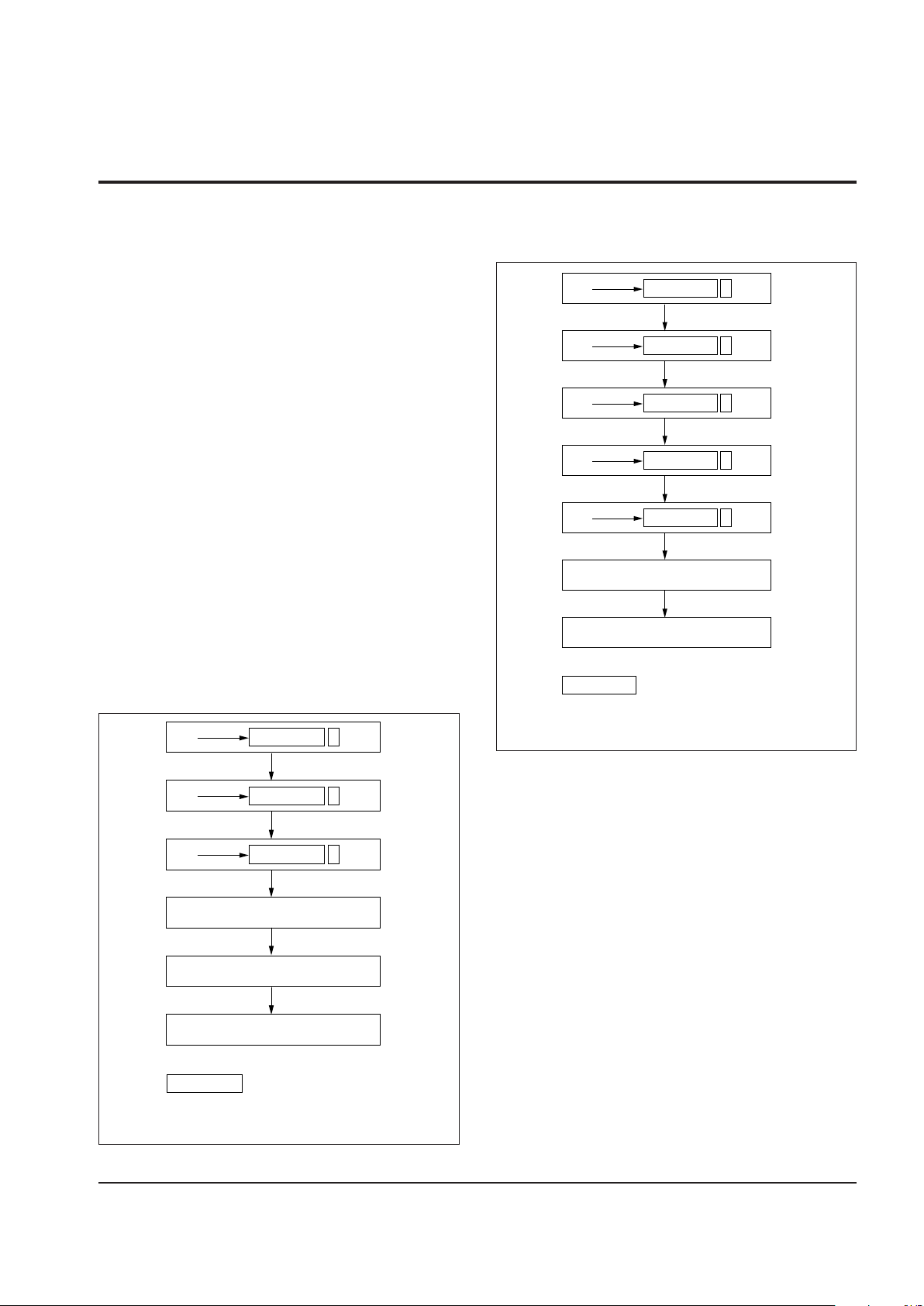
Figure 3. Sequence to Deactivate Software Data
Protection
AA
b
2
P 555b1b
0
55
b
2
AAA
AAA
b1b
0
A0
b
2
P 555b1b
0
AA
b
2
P 555b1b
0
80
b
2
P
2887 ILL F07
b1b
0
Reference the A15–A13
setting in EEM register
Delay of t
WC
Exit Routine
b2b1b
0
P
P = Address bit (A12) of the
memory plane not being read.
Page 6
X88C75 SLIC® E
2
6
that accessing the BPR automatically sets the upper
level SDP. If for some reason the user does not want
SDP enabled, they may reset it using the normal reset
command sequence. This will not affect the state of the
BPR and any 1K x 8 blocks that were set to the write
lockout state will remain in the write lockout state.
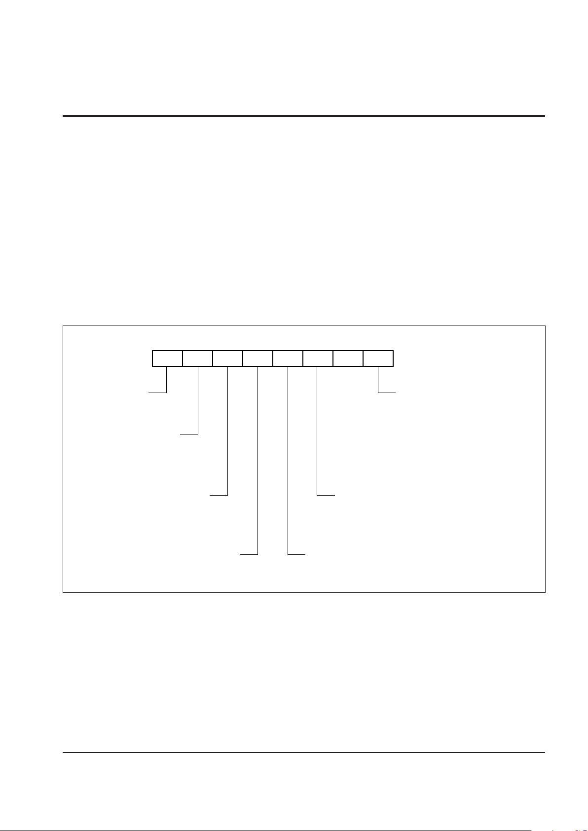
Figure 4. Block Protect Register Format
Figure 5. Setting BPR Command Sequence
The BPR format and block map are illustrated above.
The command sequence is illustrated to the right.
MSB LSB
01234567
BLOCK
ADDRESS
0000-03FF
0400-07FF
0800-0BFF
0C00-0FFF
1000-13FF
1400-17FF
1800-1BFF
1C00-1FFF
“1” = Protect, “0” = Unprotect Block Specified
2887 ILL F08.1
AA
b
2
P 555b1b
0
55
b
2
AAA
AAA
b1b
0
A0
b
2
P 555b1b
0
AA
b
2
P 555b1b
0
C0
b
2
P
2887 ILL F09.1
b1b
0
Write BPR mask value
to any address
Reference the A15–A13
setting in E2M register
Delay of t
WC
Exit Routine
(BPR Register Set Global SDP Set)
b2b1b
0
P
P = Address bit (A12) of the
memory plane not being read.
Figure 6. Microcontroller Map
0000
1FFF
FFFF
2887 ILL F29.1
RESET/ISR VECTORS
USER
APPLICATION
CODE/DATA
8K BYTES OF BYTE
ALTERABLE DUAL
PLANE ARCHITECTURED
NON-VOLATILE MEMORY
(MAPPABLE TO ANY 8K
PAGE BY THE E2M BITS 2–0)
SRF (SPECIAL FUNCTION
REGISTER) BLOCK
(MAPPABLE TO ANY 1K
PAGE BY THE SFRM
REGISTER)
0030
0150
0000
1F00
1FFF
FC00
FFFF
SLIC
SLIC
Page 7
X88C75 SLIC® E
2
7
Figure 7. On-Chip Registers
Programmable Address Decoding
The X88C75 features an internal programmable address decoder which allows the nonvolatile memory
array and the internal registers to be mapped in various
locations of the 64K-byte memory map. The register set
is mappable into a 1K-byte block, while the nonvolatile
memory array is mappable into an 8K-byte block. The
mapping is controlled by two nonvolatile configuration
registers, the SFR Map Register and the E2 Memory
Map Register. Their bits are mapped as follows:
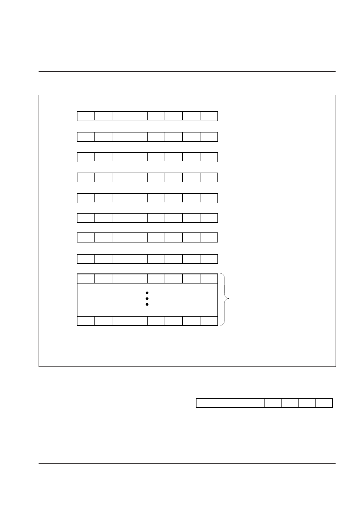
SFR Map Register (SFRM) Default = 3F
0 0 A15 A14 A13 A12 A11 A10
76
2887 ILL F10
543210
A15-A10
The A15-A10 are upper address bits for the 1K-byte
page where the SFR memory is mapped.
0
2887 ILL F30.2
0 LAM 0 RST A15 A14 A13
76543210
FC38
EEM*
E2 Memory Map Register
MSB LSB
FC08
PDRB
Port Data Register B
MSB LSB
FC10
PDRA
Port Data Register A
INT INTA INTB ENA ENB ENEE 0 EOW
FC18
ISR
Interrupt Status Register
IRST 1 AWO BWO DIRA DIRB STRA STRB
FC20
CR
Configuration Register
MSB LSB
FC28
PPRB
Port Pin Register B
MSB LSB
FC30
PPRA
Port Pin Register A
Special Function Register
Memory Map Register
0
NOTE: * The value returned by reading these registers is the complement of the
actual data. These registers are nonvolatile and a special SDP sequence
is used to alter their contents. All the other registers are initialized by a
valid reset input signal and when the device is power cycled.
0 A15 A14 A13 A12 A11 A10
FC00
SFRM*
FE00
FE0F
16 Bytes General Purpose SRAM
MSB LSB
MSB LSB
Page 8
X88C75 SLIC® E
2
8
Figure 8. Setting the SFR Map Register
Figure 9. Setting Program Memory Map Register
BITS 7:6
Setting these two bits to any combination other than “00”
or “11” will interfere with device proper operation.
E2 Memory Map Register (EEM) Default = 08
0 0 LAM 0 RST A15 A14 A13
76
2887 ILL F11
543210
A15-A13
Modifying these three bits changes the location of the
program memory within the address map.The A15-A13
correspond to the upper three address bits of the 8Kbyte page where program memory will be mapped.
RST
The RST bit controls the polarity of the RESET input pin.
“0” = RESET is Active LOW
“1” = RESET is Active HIGH
LAM
Port B can be configured as either a general purpose
I/O port (normal I/O mode), or latched address mode
(LAM). The LAM option programs port B to output the
demultiplexed low order byte of the address latched into
the X88C75 by ALE. The LAM bit selects between these
two modes.
“0” = PORT B is I/O Port
“1” = Port B outputs low address byte (A7-A0)
Setting the Mapping Registers
The mapping registers are written using a modified
version of the Software Data Protection sequence. All
timings must adhere to the normal Software Data Protection sequence.
The complemented contents of the SFR map register
and the E2 memory map register can be read by the
microcontroller at their corresponding SFR addresses.
The physical memory location of these registers can be
derived by adding the following offset to the SFR base
address:
SFR Map Register 00H
E2 Memory Map Register 38H
If the regions specified in the map registers overlap, only
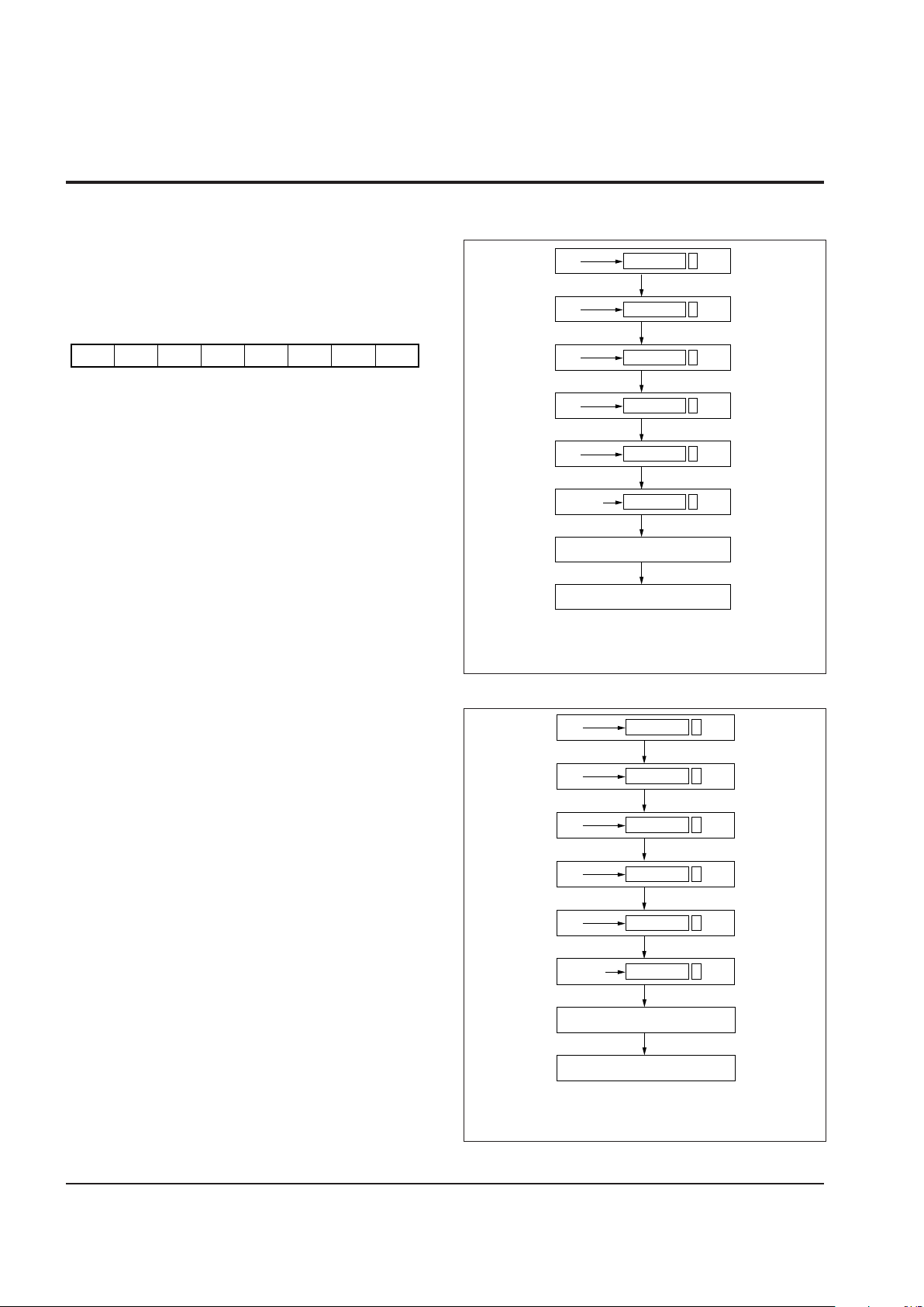
the SFR will be accessible.
AA
b
2
P 555b1b
0
55
b
2
AAA
AAA
b1b
0
A0
b
2
P 555b1b
0
AA
b
2
P 555b1b
0
D0
Delay of t
WC
Exit Routine
b
2
P
2887 ILL F12.1
b1b
0
XXX
Desired
Value
b
2Pb1b0
X = Don’t Care
B[2:0] = E2M [2:0]
P = Address bit (A12) of the
memory plane not being read.
P
AA
b
2
P 555b1b
0
55
b
2
AAA
AAA
b1b
0
A0
b
2
P 555b1b
0
AA
b
2
P 555b1b
0
E0
b
2
P
2887 ILL F13.1
b1b
0
XXX
Desired
Value
b
2Pb1b0
P
Delay of t
WC
Exit Routine
X = Don’t Care
B[2:0] = E2M [2:0]
P = Address bit (A12) of the
memory plane not being read.
Page 9
X88C75 SLIC® E
2
9
Interrupt Status Register (ISR)
The Interrupt Status Register is a volatile register used
to configure the interrupt condition for the I/O ports as
well as to determine the interrupt status of the ports. The
X88C75 ports can generate an interrupt to the microcontroller upon the proper transition (as specified in the
configuration register) on either STRA or STRB pins
when the corresponding I/O port is configured as an
input.
The INT flag is set when any of the input strobes are
toggled provided that their corresponding interrupt enable bits (ENA, ENB) are set. The INT flag is cleared
when latched data is read (PDR) or pending interrupt
status flag (INTA, INTB) in ISR is forced to “0” by the
interrupt service routine. Interrupt service routine should
examine the interrupt status flags (INTA, INTB) and
identify the source of pending interrupt.
The E2 memory interrupt status flag (EOW) is another
means to detect the early completion of a write cycle.
When ENEE is enabled, the hardware will set the EOW
flag, and interrupt the microcontroller at the end of an
internal programming cycle. Toggle Bit Polling can be
replaced by this hardware interrupt, which reduces the
software overhead. The EOW flag should be cleared by
software. The interrupt status register bits are mapped
as follows.
Figure 10. Interrupt Status Register
INT
2887 ILL F14.1
INTA INTB ENA ENB ENEE 0 EOW
76543210
Interrupt Flag
“0” = No pending interrupt
“1” = Interrupt request
Port B – Interrupt Status
“0” = No pending interrupt
“1” = Port B latched data when a valid
transition occurred on the STRB
and port B was an input port.
Port A – Interrupt Enable
“0” = Mask off interrupt
“1” = Interrupt enabled
Port B – Interrupt Enable
“0” = Mask off interrupt
“1” = Interrupt enabled
EEPROM Interrupt Enable
“0” = Mask off interrupt
“1” = Interrupt enabled
EEPROM Interrupt Status
“0” = Programming in progress
“1” = Set by hardware when it completes
programming the previously
written data
Port A – Interrupt Status
“0” = No pending interrupt
“1” = Port A latched data when a valid
transition occurred on the STRA
and port A was an input port.
Page 10

X88C75 SLIC® E
2
10
Configuration Register (CR)
The Configuration Register is a volatile register used to
configure the operation of the I/O ports. The configuration register allows the microcontroller to designate
whether each of the two ports is an input or output, what
type of output drive is to be used, and what is the polarity
of the two strobe lines, STRA and STRB. The bit map
of configuration register is shown below.
The IRST bit in the configuration register controls the
method used to clear the port interrupt request
flags(INTA, INTB). The interrupts are reset by either
reading the interrupt source or writing to the Interrupt
Status Register. The interrupt must be disabled prior to
changing strobe polarity bits(STPA, SPTB), or port
direction bits (DIRA, DIRB) in CR. Otherwise, any attempt to modify status of these bits may cause an
interrupt to occur.
Port Data Registers (PDR)
The PDRA/PDRB are byte-wide latches which hold port
data. When a port is configured as output, the outputs
of its PDR latch are connected to the port pins. Writing
to PDR generates a pulse on the port strobe pin and
latches the data. If a port is configured as an input, the
inputs of its PDR latch are connected to the port pins.
External data is latched into PDR on the positive edge of
its clock. The port strobe input and strobe polarity bit
(STPA, STPB) are XORed to generate the PDR
input clock.
Port Pin Registers (PPR)
The read-only Port Pin Registers are used for reading
the current status of the external I/O port pins. Accessing
the PPR causes the values on the port pins to be placed
on the data bus.
The port direction control bits in configuration register
set the direction for the entire port and no control
mechanism is provided to program the direction of
individual pins. However, the ports have a flexible architecture which allows operating the I/O ports in bidirectional mode using the PPR read feature.
A port can be operated in input/output mode by configuring it as an open-drain output port. The port wire-OR
bit (AWO, or BWO in CR) and its port data direction bit
(DIRA, or DIRB in CR) should be set to “1”. The PDR bits
which correspond to the port pins assigned as inputs
should be programmed to “1”. For monitoring the status
of the input pins, the PPR can be read. In this application
the port strobe pin and the PDR latch are in output mode.
In open-drain mode, there are weak internal pull-ups on
the port pins, however external pull-ups must be used for
proper switching of the I/O lines.
STATIC RAM BLOCK
There are 16 bytes of volatile static RAM registers
mapped to the SFR region. They reside in the 200H20FH area offset from the SFR base address. Accessing these registers has to be done through external RAM
operations for both writes and reads.
IRST
2887 ILL F15.1
1 AWO BWO DIRA DIRB STPA STPB
76543210
Interrupt Request Reset Mode
This bit controls the clearing of the
interrupt request flag.
“0” = Reading the interrupt source
“1” = Writing to the request register
Port A – Outputs
“0” = CMOS
“1” = Open-Drain
Port B – Outputs
“0” = CMOS
“1” = Open-Drain
Port A – Direction Flag
“0” = Input mode
“1” = Output mode
Port B – Direction Flag
“0” = Input mode
“1” = Output mode
Strobe B – Strobe Pin Polarity
“0” = Active LOW
“1” = Active HIGH
Strobe A – Strobe Pin Polarity
“0” = Active LOW
“1” = Active HIGH
Figure 11. Configuration Register
Page 11

X88C75 SLIC® E
2
11
PRINCIPLES OF OPERATION
I/O Port Operation
The expansion ports are accessible to the software
using their assigned memory mapped addresses. Each
port occupies two addresses in the SFR plane, the Port
Data Register and Port Pin Register. These registers
and their location in the 1K-byte register memory space
is shown on page 7.
The ports can be configured as either inputs or outputs,
the DIRA and DIRB bits in the configuration register are
used to select between the modes. The input signal on
the strobe pin, when the corresponding port is configured as an input, is fed to the clock input of the port latch.
These are transparent latches and the trailing edge of
the strobe pulse is used to latch the data present on the
input pins. The strobe signal polarity is configurable
using the STPA and STPB bits in the configuration
register.
Writing to the port data register of an output port will
generate a pulse of fixed duration on its strobe pin. The
data also simultaneously arrives at the port output pins.
The latched data stays there until new data is written to
the port data register. The strobe pulse shape is controlled by the state of the STPA and STPB bits in the
configuration register. A “1” forces the valid transition on
the corresponding strobe pin as active HIGH ( ),
and a “0” sets it to active LOW ( ).
When an external strobe signal is applied to an input
port, the latching of input data is followed by the setting
of the interrupt flags. The INTA and INTB interrupt flags
are used by ports A and B respectively, and are set along
with the INT interrupt flag at the end of strobe pulse input.
External interrupt (IRQ) is generated if the interrupt
enable flags (ENA and ENB) are set by the software.
The former enables the port A interrupt and the latter
enables the port B interrupt.
The port output drivers can be either CMOS or opendrain. The wire-OR bits (AWO, BWO) in the configuration register are used to make the selection. When the
bits are “0” the CMOS drivers are enabled. Setting these
bits will enable the open-drain output drivers. Small pullup resistors should be used on the pins of open-drain
ports.
INTERNAL DATA BUS
I/O
PIN
PORT
OUTPUT
OUTPUTINPUT
LATCH FOR
I/O PIN
PORT WRITE
(PORT OUTPUT)
STROBE (PORT INPUT)
2887 ILL F16.1
PORT READ
(PORT INPUT)
PIN READ
(PORT IN OR OUTPUT)
Figure 12. Block Diagram of the I/O Ports
Page 12

X88C75 SLIC® E
2
12
IRQ
The IRQ pin is an active LOW open-drain output. In
embedded systems applications, this signal is connected to the microcontroller interrupt input pin through
either a direct connection or via an interrupt controller.
Table 1 depicts the three sources of interrupts and their
associated flags. Under normal conditions, the INT and
port interrupt flags are set, if the port which is configured
as an input has its strobe line toggled. If the port interrupt
enable flag is set, or gets set while the INT flag is set,
then the IRQ signal is asserted. The IRQ stays valid as
long as the interrupt flags are not cleared by the software
or the hardware.
Another interrupt source is the End Of Write flag (EOW)
which is set by the hardware at the end of every internal
programming cycle. The interrupt from this source is
controlled by the ENEE bit in ISR. If ENEE is enabled,
then EOW can generate an external interrupt. The
interrupt is cleared by setting EOW to “0”.
Table 1. X88C75 Interrupt Sources
Interrupt Interrupt Status INT
Source Enable Flag Flag
PORT A ENA INTA “1”
PORT B ENB INTB “1”
EOW ENEE EOW —
2887 PGM T02.1
SOFTWARE CONTROLLED PORT OPERATIONS
The individual clock signals, that control the PDR input
latches and load the external data present on the port
pins, are generated by XORing the strobe polarity bit
and the strobe input of the port. The strobe polarity bits
(STPA, STPB) in CR can be used to program the active
edge of the strobe inputs. However, if the external
strobe input is permanently tied to VSS or VCC, then the
strobe polarity bit controls the PDR input latch clock
signal.
When a port strobe and its polarity bit have identical
logic levels, the corresponding PDR latch is active and
any change in the port inputs will show up at the PDR
latch outputs. Holding the strobe input at current levels
and changing the strobe polarity bit value will generate
a positive transition on the PDR clock signal, causing
the latch outputs to reflect the previous logic state of the
port pins. The clock transition sets the interrupt flags,
and if the interrupts have been enabled, then an external
interrupt signal will be asserted.
This feature allows the port input operation by permanently tying the STRx inputs to VCC or VSS, and using
the STPx bits in CR to control PDR latches. Another
advantage of this feature are software generated interrupts. Since the clocking of the PDR latch causes the
corresponding port INTx flags to be set, by enabling the
interrupts the microcontroller is forced to execute the
ISR responsible to service the newly latched data.
END OF WRITE (EOW) INTERRUPT
The internal programming cycle requires several milliseconds for either a single byte write or a page write.
The updated memory plane is inaccessible while the
programming is in progress. However, the opposite
plane is still available for program fetch and data read
operations.
The X88C75 has two means of signaling end of an
internal programming cycle. In the Toggle Bit Polling
technique, the last written byte is successively read. Bit
6 of read data toggles while the programming cycle is
still in progress. The software has to continually monitor
device responses and determine if it can again access
the plane.
In the other method, at the end of an internal programming cycle, the hardware sets the EOW flag. The
software can either poll this flag or enable the interrupts
by setting the ENEE bit in ISR. Effective use of EOW is
made by clearing it prior to initiating a write operation. If
PORTS A & B INTERRUPTS
The X88C75 features two 8-bit I/O ports which are
equipped with a configurable interrupt module. The
interrupts are used to signal the reception of new data at
an input port data latch. When a port is configured as an
output, it can no longer generate any interrupts.
The input port interrupt mechanism is controlled by the
external strobe pins (STRA, STRB). Detecting a valid
transition on the pin will set the interrupt flags and latch
in the input data. The external interrupts from the ports
can be masked off using the interrupt enable bits (ENA,
ENB) in ISR.
Once an external interrupt is asserted, clearing the
interrupt flags will cause the IRQ signal to return to its
idle state. There are two ways of resetting the interrupt
flags. The selection is made using the IRST bit in the
configuration register. If IRST is set, then the interrupt
flags are cleared by writing “0” to the bit positions
corresponding to the interrupt flags (INTA, INTB) in ISR.
When the IRST is cleared, reading the PDR automatically clears the interrupt flags.
Page 13

X88C75 SLIC® E
2
13
reload value for 9600 baud rate and write it into the
X88C75 location 00E8H. The XSLIC software, a PC
based communication driver, automates changing of
the default parameters when using its SETUP option
menu. The boot-firmware (SLIC) residing on the X88C75
contains a lookup table which can be accessed from the
subroutine (EXEC_SUB), located at location 0126H.
Two bytes are used per table entry. The EXEC_SUB
input requirements are as follows:
R0 = Contains a Function Number from the following
Function Table.
The table entry at location (014E-014FH) is reserved for
user’s application code. This function will be executed
on power-up if the SLIC receives any characters other
than those for the RESET (ASCII ‘R’), or ID (ASCII ‘X’)
commands. The table entry can be changed to point to
other code responsible for power-up initialization. This is
preferred method than changing the reset vector, since
the SLIC code can still be invoked upon power-up.
Other functions available through the EXEC_SUB calls
is as follows:
the interrupt is enabled, an external interrupt will be
asserted at the completion of the internal write cycle.
The interrupt is cleared by setting EOW to “0”.
USING A PORT IN BIDIRECTIONAL MODE
In order to use a port in bidirectional mode, it has to be
configured as an open drain output port. Small pull-up
resistors are required on all port output pins. Bit positions in the Port Data Register corresponding to port
inputs should contain “1”. The inputs are then read by
accessing PPR. Data is not latched into the device, so
the inputs must stay valid throughout the read cycle. The
port strobe pin is configured as an output and cannot be
used as port latch clock input.
The current version of the SLIC E2 configures the 80C51
serial port to the variable baud rate mode. It sets a timer
1 reload value for a system clock rate of 11.059MHz. For
other clock rates end user must recalculate timer 1
SLIC FUNCTIONS (80C51 Specific SLIC)
The resident SLIC E2 has designated memory spaces
allocated for its use. The user’s application code should
avoid using these areas as part of its code segment,
otherwise it will overwrite the SLIC E2. Version 3.0 of the
X88C75 SLIC E2 occupies 256 bytes in the upper
memory bank, starting at address 1F00H, and 288 bytes
in the lower bank’s address range 30H-14FH. Prior to
downloading code, assemble and link the source files
using the above address information. Use memory
space taken up by the SLIC E2 as a run-time data
storage, if there is no further need to modify the X88C75
SLIC E2 content.
FUNCTION NO. DESCRIPTION
0 - PROC_PROG Download and program a
page
1 - PROC_BPR Program BPR
2 - RESET Start execution from
location 0000H
3 - PROC_VER Download and verify a page
4 - DUMMY Command not recognized
5 - INIT_UART Initialize UART parameters
to default
6 - PROG_PG Program a page
7 - SEND_CHAR Send a character to the
UART
8 - GET_CHAR Read a character from the
RAM receive buffer (40H-5FH)
9 - SDP_HI_PLANE Generate SDP off sequence
for upper plane
10- SDP_LO_PLANE Generate SDP off sequence
for lower plane
11- USER_CODE Execute user’s code
2887 PGM T03.1
For detailed information about the listed functions, including their input requirements, refer to the SLIC software specification document.
SLIC
0000H
0030H
0150H
01F00H
SLIC
User’s Program/Data
2887 ILL F17
ISR & Reset Vectors
Figure 13.
Page 14

X88C75 SLIC® E
2
14
Example 2
Applications requiring more than 8K bytes of program
memory space can be implemented using the basic
system architecture depicted in example 1 along with an
additional memory device such as the X28C256. Since
this device requires non-multiplexed address/data buses,
the X88C75 LAM feature is used to output the low order
address byte. The SFRM can be mapped to any 64x1K
page, but the X28C256 should be mapped to the upper
program memory address space and out of the E2M
address range (0000-1FFFH.) This technique may also
be used for other external byte wide memories such as
SRAMs or EPROMs.
APPLICATION EXAMPLES
This section gives examples of most widely used embedded systems architectures using the X88C75 and
80C51 microcontroller. However, keep in mind that
other microcontrollers are also supported by the X88C75
and/or other SLIC devices that Xicor manufactures.
Example 1
In this system, the X88C75 is the only parallel device
residing on the multiplexed address and data bus. There
may be other peripherals on the system board which are
controlled by the ports on the X88C75. This configuration maps the EEM to a program/data memory address
in the range of 0000-1FFFH. The SFRM can be mapped
to any of the 64 x 1K pages within the data memory
space.
Figure 14. Example 1
ALE
WR
RD
PSEN
ALE
WR
RD
PSEN
CE
CE
OE
WE
I/O7-I/O0
A14-A8
EA
A15
2887 ILL F19
PB A7-A0
STRA
PA
A7:0
8
X88C758051
X28C256
A15:8
AD7:0
D7:0
A15:8
STRB
RESET
Figure 15. Example 2
ALE
WR
RD
PSEN
ALE
WR
RD
PSEN
CE
EA
STRA
PA
X88C758051
A15:8
AD7:0
STRB
2887 ILL F18
PB
RESET
Page 15

X88C75 SLIC® E
2
15
Example 3
If an application requires larger program memory storage and both extra ports, then example 2 does not meet
this requirement. Since the LAM feature uses port B to
output the non-multiplexed address, then port B cannot
be also used as general purpose I/O. The solution to this
problem is to use X68C64, which interfaces to a multiplexed bus and takes an active HIGH CE input. Example
3 maps the X68C64 to the top 8K program memory
space in the range of 8000-FFFFH. This approach
provides a total of 16K-bytes of program memory. Using
the same approach, two additional X68C64 device can
be added and A13-A14 can be used as their CE inputs,
Figure 17. Example 4
Figure 16. Example 3
for the total of 32K-bytes of program memory. Ports A
and B are still available to handle any general purpose
I/O functions.
Example 4
For those applications using extensive I/O, up to 128
I/O pins are obtained by placing 8 of the X88C75 devices
on the same bus. This approach gives a total of 64Kbytes of program memory space, and 128 I/O pins. Note
that the SFRM can overlap the E2M address space,
however, only the SFR resources are accessible and
the associated E2 memory location are not available.
ALE
WR
RD
PSEN
ALE
WR
RD
PSEN
CE
CE
E
AS
SEL
WR
A/D7-A/D0
A12-A8
EA
A15
2887 ILL F20
STRA
PA
X88C758051
X68C64
A15:8
AD7:0
AD7:0
A15:8
STRB
PB
RESET
ALE
WR
RD
PSEN
EA
X88C75
8051
A15:8
2887 ILL F21
AD7:0
PA
ALE
WR
RD
PSEN
CE
STRB
PB
STRA
128 I/O
RESET
Page 16

X88C75 SLIC® E
2
16
Notes: (3) VIL min. and VIH max. are for reference only and are not tested.
(4) This parameter is periodically sampled and not 100% tested.
CAPACITANCE TA = +25°C, f = 1MHz, VCC = 5V
Symbol Test Max. Units Conditions
C
I/O
(4)
Input/Output Capacitance 10 pF V
I/O
= 0V
C
IN
(4)
Input Capacitance 6 pF V
IN
= 0V
2887 PGM T07
POWER-UP TIMING
Symbol Parameter Max. Units
t
PUR
(4)
Power-Up to Read 1 ms
t
PUW
(4)
Power-Up to Write 5 ms
2887 PGM T08
D.C. OPERATING CHARACTERISTICS (Over recommended operating conditions unless otherwise specified.)
Limits
Symbol Parameter Min. Max. Units Test Conditions
I
CC
VCC Current (Active) 60 mA CE = RD = VIL, All I/O’s =
Open,Other Inputs = V
CC
I
SB1(CMOS)VCC
Current (Standby) 100 µA CE = VIH, All I/O’s = Open, Other
Inputs = VCC – 0.3V, ALE = V
IL
I
SB2(TTL)
VCC Current (Standby) 2 mA CE = VIH, All I/O’s = Open, Other
Inputs = VIH, ALE = V
IL
I
LI
Input Leakage Current 10 µAV
IN
= VSS to V
CC
I
LO
Output Leakage Current 10 µAV
OUT
= VSS to VCC,
RD = PSEN = V
IH
V
lL
(3)
Input LOW Voltage –1 0.8 V
V
IH
(3)
Input HIGH Voltage 2 VCC + 0.5 V
V
OL
Output LOW Voltage 0.4 V IOL = 2.1mA
V
OH
Output HIGH Voltage 2.4 V IOH = –400µA
2887 PGM T06.2
RECOMMENDED OPERATING CONDITIONS
Temperature Min. Max.
Commercial 0°C +70°C
Industrial –40°C +85°C
Military –55°C +125°C
2887 PGM T04.1
Supply Voltage Limits
X88C75 5V ±10%
2887 PGM T05.1
ABSOLUTE MAXIMUM RATINGS*
Temperature under Bias .................. –65°C to +135°C
Storage Temperature .......................–65°C to +150°C
Voltage on any Pin with
Respect to VSS.................................. –1V to +7V
D.C. Output Current ............................................5 mA
Lead Temperature
(Soldering, 10 seconds).............................. 300°C
*COMMENT
Stresses above those listed under “Absolute Maximum
Ratings” may cause permanent damage to the device.
This is a stress rating only and the functional operation of
the device at these or any other conditions above those
indicated in the operational sections of this specification is
not implied. Exposure to absolute maximum rating conditions for extended periods may affect device reliability.
Page 17

X88C75 SLIC® E
2
17
Note: (5) This parameter is periodically sampled and not 100% tested.
PSEN Controlled Read Timing Diagram
PSEN Controlled Read Cycle
Symbol Parameter Min. Max. Units
t
LHLL
ALE Pulse Width 80 ns
t
AVLL
Address Setup Time 20 ns
t
LLAX
Address Hold Time 30 ns
t
PLDV
PSEN Read Access Time 120 ns
t
PHDX
Data Hold Time 0 ns
t
ELLL
Chip Enable Setup Time 7 ns
PW
PL
PSEN Pulse Width 150 ns
t
PS
PSEN Setup Time 30 ns
t
PH
PSEN Hold Time 20 ns
t
PHDZ
(5)
PSEN Disable to Output in High Z 50 ns
t
PLDX
(5)
PSEN to Output in Low Z 10 ns
2887 PGM T10
EQUIVALENT A.C. TEST CIRCUITA.C. CONDITIONS OF TEST
Input Pulse Levels 0V to 3V
Input Rise and Fall Times 10ns
Input and Output Timing Levels 1.5V
2887 PGM T09.1
A.C. CHARACTERISTICS (Over the recommended operating conditions unless otherwise specified.)
ALE
A/D0–A/D
7
A8–A
12
PSEN
A
IN
t
PLDV
D
OUT
2887 ILL F23
t
PH
t
PH
t
LHLL
t
AVLL
t
LLAX
t
PS
PW
PL
ADDRESS
CE
t
PLDX
t
PHDZ
t
PHDX
t
ELLL
2887 ILL F22.2
5V
1.92KΩ
100pF
OUTPUT
1.37KΩ
Page 18

X88C75 SLIC® E
2
18
RD Controlled Read Cycle
Symbol Parameter Min. Max. Units
t
LHLL
ALE Pulse Width 80 ns
t
AVLL
Address Setup Time 20 ns
t
LLAX
Address Hold Time 30 ns
t
RLDV
RD Read Access Time 120 ns
t
RHDX
Data Hold Time 0 ns
t
ELLL
Chip Enable Setup Time 7 ns
PW
RL
RD Pulse Width 150 ns
t
RDS
RD Setup Time 30 ns
t
RDH
RD Hold Time 20 ns
t
RHDZ
(6)
RD Disable to Output in High Z 50 ns
t
RLDX
(6)
RD to Output in Low Z 0 ns
2887 PGM T11
RD Controlled Read Timing Diagram
Note: (6) This parameter is periodically sampled and not 100% tested.
ALE
A/D0–A/D
7
A8–A
12
RD
A
IN
t
RLDV
D
OUT
2887 ILL F24
t
RDH
t
RDH
t
LHLL
t
AVLL
t
LLAX
t
RDS
PW
RL
ADDRESS
CE
t
RLDX
t
RHDZ
t
RHDX
t
ELLL
Page 19

X88C75 SLIC® E
2
19
WR Controlled Write Cycle
Symbol Parameter Min. Max. Units
t
LHLL
ALE Pulse Width 80 ns
t
AVLL
Address Setup Time 20 ns
t
LLAX
Address Hold Time 30 ns
t
DVWH
Data Setup Time 50 ns
t
WHDX
Data Hold Time 30 ns
t
ELLL
Chip Enable Setup Time 7 ns
t
WLWH
WR Pulse Width 120 ns
t
WRS
WR Setup Time 30 ns
t
WRH
WR Hold Time 20 ns
t
BLC
Byte Load Time (Page Write) 0.5 100 µs
t
WC
(7)
Write Cycle Time 5 ms
2887 PGM T12
WR Controlled Write Timing Diagram
Note: (7) tWC is the minimum cycle time to be allowed from the system perspective unless polling techniques are used. It is the maximum
time the device requires to automatically complete the internal write operation.
ALE
A/D0–A/D
7
A8–A
12
WR
A
IN
t
DVWH
D
IN
2887 ILL F25
t
WHDX
t
WRH
t
WRH
t
LHLL
t
AVLL
t
LLAX
t
WRS
t
WLWH
ADDRESS
CE
t
ELLL
Page 20

X88C75 SLIC® E
2
20
Port Read Diagram
PORT READ TIMING
No. Symbol Parameter Min. Max. Units
1t
SVSX
Strobe Pulse Width 80 ns
2t
DVSV
Data Port Setup 20 ns
3t
SVDX
Data Port Hold Time 30 ns
4t
SVIV
Interrupt Request to Strobe 50 ns
5t
IAD
IRQ to ALE 0 ns
6t
LHLL
ALE Pulse Width 80 ns
7t
RXIX
RD to IRQ 30 ns
8t
AVLL
Address setup time 20 ns
9t
LLAX
Address hold time 30 ns
10 t
LLWL
ALE to RD LOW 30 ns
11 t
RLDV
RD Access Time 120 ns
2887 PGM T13.2
STRA/STRB* (IN)
PA7:0/PB7:0
IRQ
2887 ILL F26.1
ALE
A15–A8
RD/PSEN
AD7–AD0
1
32
4
7
6
5
8
9
10
8 9 11
INTERRUPT
RECOGNIZED
PORT
ADDRESS
A7-A0
DATA
VALID
NOTE: *Figure shows active HIGH strobes.
DATA VALID
Page 21

X88C75 SLIC® E
2
21
Port Write Diagram
PORT WRITE TIMING
No. Symbol Parameter Min. Max. Units
1t
LHLL
ALE Pulse Width 80 ns
2t
WCS
Write Chip Select Setup Time 20 ns
3t
LLWL
ALE to WR 10 ns
4t
WLWH
WR Pulse Width 120 ns
5t
AVLL
Write Address Setup Time 20 ns
6t
LLAX
Write Address Hold Time 30 ns
7t
DVWH
Data Setup Time 50 ns
8t
WHDX
Data Hold Time 10 ns
9t
SVSX
Strobe Pulse Width 120 ns
10 t
QVSV
Strobe Access Time 40 ns
11 t
POS
Port Output Setup Time 40 ns
2887 PGM T14.1
A15–A8
CE
ALE
WR
AD7–AD0
STRA/STRB* (OUT)
PA7:0 / PB7:0
2887 ILL F27.1
5
1
2
6
3 4
5
6
11
9
7
8
10
ADDRESS
A0-A15
ADDRESS
A7-A0
DATA VALID
VALID NEW DATAPREVIOUS DATA
NOTE: *Figure shows active HIGH strobes.
Page 22

X88C75 SLIC® E
2
22
LAM (Latch Address Mode) Diagram
LAM TIMING
No. Symbol Parameter Min. Max. Units
1t
LHLL
ALE Pulse Width 80 ns
2t
AVLL
Address Setup Time 20 ns
3t
LLAX
Address Hold Time 30 ns
4t
POS
Port Output Setup Time 20 ns
2887 PGM T15
A15–A8
ALE
AD7–AD0
PB7:0
2887 ILL F31
2
1
3
2
3
4
ADDRESS
A15-A8
ADDRESS
A7-A0
DATA VALID
ADDRESS A7–A0
SYMBOL TABLE
WAVEFORM
INPUTS
OUTPUTS
Must be
steady
Will be
steady
May change
from LOW
to HIGH
Will change
from LOW
to HIGH
May change
from HIGH
to LOW
Will change
from HIGH
to LOW
Don’t Care:
Changes
Allowed
Changing:
State Not
Known
N/A
Center Line
is High
Impedance
Page 23

X88C75 SLIC® E
2
23
PACKAGING INFORMATION
3926 FHD F43.1
NOTE:
1. ALL DIMENSIONS IN INCHES (IN PARENTHESES IN MILLIMETERS)
2. PACKAGE DIMENSIONS EXCLUDE MOLDING FLASH
0.022 (0.56)
0.014 (0.36)
0.200 (5.08)
0.115 (2.92)
0.625 (15.88)
0.590 (14.99)
0.110 (2.79)
0.090 (2.29)
2.480 (62.99)
2.385 (60.58)
2.300 (58.42)
REF.
PIN 1 INDEX
0.195 (4.95)
0.125 (3.18)
0.030 (0.76)
0.015 (0.38)
PIN 1
SEATING
PLANE
0.070 (17.78)
0.030 (7.62)
0.580 (14.73)
0.485 (12.32)
0.088 (2.24)
0.040 (1.02)
0°
15°
48-LEAD PLASTIC DUAL IN-LINE PACKAGE TYPE P
TYP. 0.010 (0.25)
Page 24

X88C75 SLIC® E
2
24
PACKAGING INFORMATION
0.500 (12.70)
REF.
0.655 (16.64)
0.650 (16.51)
0.695 (17.65)
0.685 (17.40)
PIN 1
0.500
(12.70)
REF.
0.050
(1.27)
REF.
0.655 (16.64)
0.650 (16.51)
0.695 (17.65)
0.685 (17.40)
0.021 (0.63)
0.013 (0.33)
0.630 (16.00)
0.590 (14.99)
0.032 (0.81)
0.026 (0.66)
0.156 (3.96)
0.145 (3.68)
0.011 (0.28)
0.009 (0.23)
0.180 (4.57)
0.165 (4.19)
0.110 (2.79)
0.100 (2.54)
—
0.020 (0.51)
SEATING PLANE
±0.004 LEAD
CO – PLANARITY
44-PIN PLASTIC LEADED CHIP CARRIER PACKAGE TYPE J
NOTES:
1. ALL DIMENSIONS IN INCHES (IN PARENTHESES IN MILLIMETERS)
2. DIMENSIONS WITH NO TOLERANCE FOR REFERENCE ONLY
3926 ILL F29.2
Page 25

X88C75 SLIC® E
2
25
PACKAGING INFORMATION
A2
A1
L1
GAGE PLANE 0.25
C
7°±0°
3926 ILL F36.4
He
D
e
b
Hd
E
NOTES:
1. GAGE PLANE DIMENSION IS IN MM.
2. LEAD COPLANARITY SHALL BE 0.10MM [0.004] MAXIMUM.
44-LEAD THIN QUAD FLAT PACK (TQFP) PACKAGE TYPE L
PIN 1
DIM
INCHESMILLIMETERS
MIN MAX
MIN MAX
A
1
A
2
b
c
D
E
e
Hd
He
L
1
0.05
1.35
0.22
0.090
9.90
9.90
11.90
11.90
0.15
1.45
0.38
0.200
10.10
10.10
12.10
12.10
0.002
0.053
0.009
0.004
0.390
0.390
0.468
0.468
0.006
0.057
0.015
0.008
0.398
0.398
0.476
0.476
1.00 TYP
0.039 TYP
0.80 TYP
0.031 TYP
Page 26

X88C75 SLIC® E
2
26
NOTES
Page 27

X88C75 SLIC® E
2
27
ORDERING INFORMATION
Device
Temperature Range
Blank = Commercial = 0°C to +70°C
I = Industrial = –40°C to +85°C
M = Military = –55°C to +125°C
Package
P = 48-Lead Plastic DIP
J = 44-Lead PLCC
L = 44-Lead TQFP
X88C75 X X SLIC
LIMITED WARRANTY
Devices sold by Xicor, Inc. are covered by the warranty and patent indemnification provisions appearing in its Terms of Sale only. Xicor, Inc. makes
no warranty, express, statutory, implied, or by description regarding the information set forth herein or regarding the freedom of the described
devices from patent infringement. Xicor, Inc. makes no warranty of merchantability or fitness for any purpose. Xicor, Inc. reserves the right to
discontinue production and change specifications and prices at any time and without notice.
Xicor, Inc. assumes no responsibility for the use of any circuitry other than circuitry embodied in a Xicor, Inc. product. No other circuits, patents,
licenses are implied.
US. PATENTS
Xicor products are covered by one or more of the following U.S. Patents: 4,263,664; 4,274,012; 4,300,212; 4,314,265; 4,326,134; 4,393,481;
4,404,475; 4,450,402; 4,486,769; 4,488,060; 4,520,461; 4,533,846; 4,599,706; 4,617,652; 4,668,932; 4,752,912; 4,829,482; 4,874,967;
4,883,976; 4,980,859; 5,012,132; 5,003,197; 5,023,694. Foreign patents and additional patents pending.
LIFE RELATED POLICY
In situations where semiconductor component failure may endanger life, system designers using this product should design the system with
appropriate error detection and correction, redundancy and back-up features to prevent such an occurrence.
Xicor’s products are not authorized for use as critical components in life support devices or systems.
1. Life support devices or systems are devices or systems which, (a) are intended for surgical implant into the body, or (b) support or sustain life,
and whose failure to perform, when properly used in accordance with instructions for use provided in the labeling, can be reasonably expected
to result in a significant injury to the user.
2. A critical component is any component of a life support device or system whose failure to perform can be reasonably expected to cause the failure
of the life support device or system, or to affect its safety or effectiveness.
 Loading...