

Page 1
Xicor, Inc. 1994, 1995, 1996 Patents Pending
7052 10/7/97 T0/C0/D0 SH
1
Characteristics subject to change without notice
128K
X76F128
16Kx8+64x8
Functional Diagram
Secure SerialFlash
FEATURES
• 64-bit Password Security
—Five 64-bit Passwords for Read, Program
and Reset
• 16384 Byte+64 Byte Password Protected Arrays
—Seperate Read Passwords
—Seperate Write Passw ords
—Reset Password
• Programmable Passwords
• Retry Counter Register
—Allows 8 tries before clearing of both arrays
—Password Protected Reset
• 32-bit Response to Reset (RST Input)
• 64 byte Sector Program
• 400kHz Clock Rate
• 2 wire Serial Interface
• Low Power CMOS
—2.7 to 5.5V operation
—Standby current Less than 1 µ A
—Active current less than 3 mA
• High Reliability Endurance:
—100,000 Write Cycles
• Data Retention: 100 years
• Available in:
—SmartCard Module
—TQFP Package
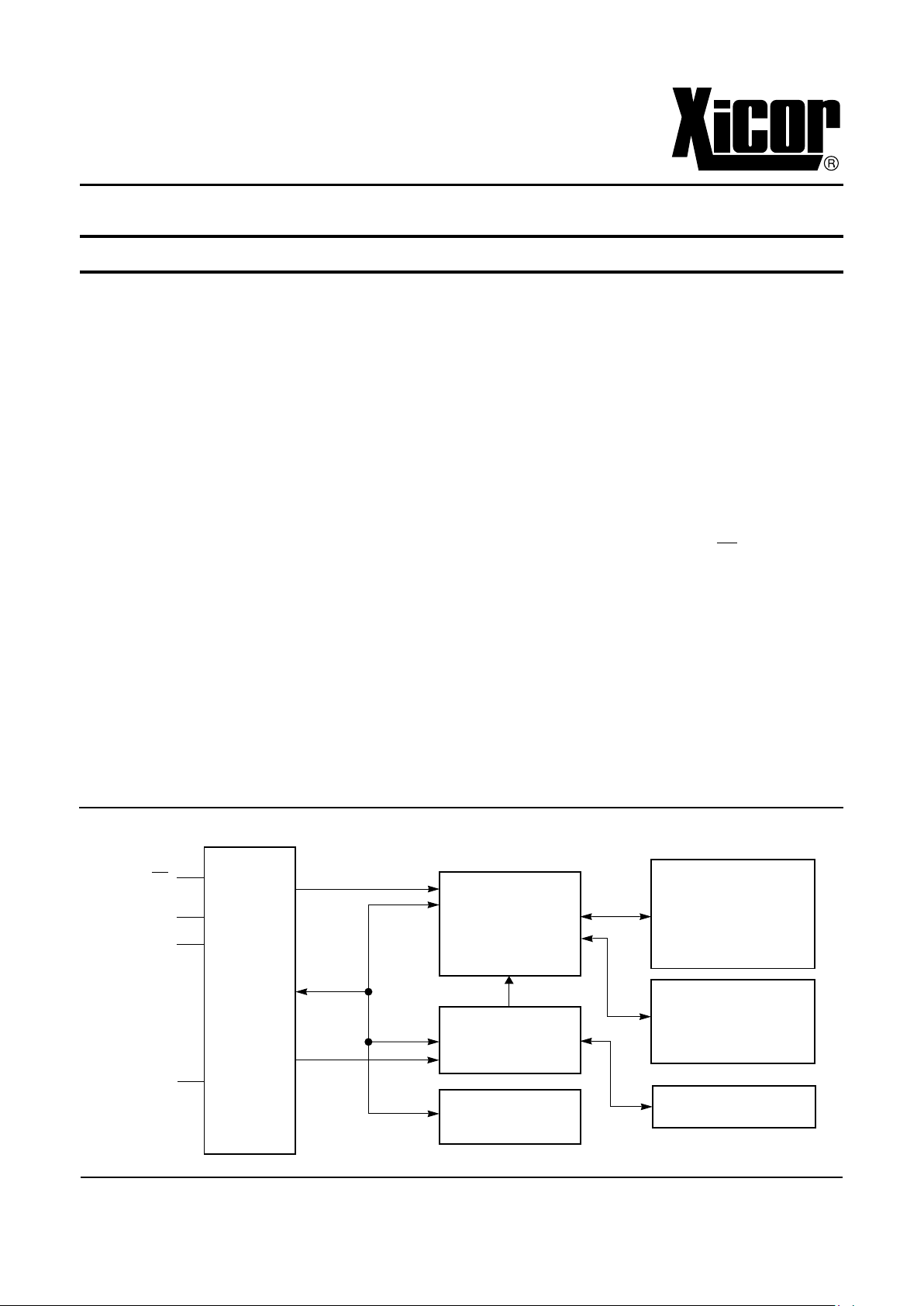
DESCRIPTION
The X76F128 is a Pass word Access Security Supervisor,
containing one 131072-bit Secure SerialFlash array and
one 512-bit Secure SerialFlash array. Access to each
memory array is controlled by two 64-bit passwords.
These passwords protect read and write operations of
the memory array. A separate RESET password is used
to reset the passwords and clear the memory arrays in
the event the read and write pass words are lost.
The X76F128 features a serial interface and software
protocol allowing operation on a popular two wire bus.
The bus signals are a clock Input (SCL) and a bidirectional data input and output (SDA). Access to the device
is controlled through a chip select (CS
) input, allowing
any number of devices to share the same b us.
The X76F128 also features a synchronous response to
reset providing an automatic output of a hard-wired 32-bit
data stream conforming to the industry standard for
memory cards.
The X76F128 utilizes Xicor’s proprietary Direct Write
TM
cell, providing a minimum endurance of 100,000 cycles
and a minimum data retention of 100 years.
LOGIC
CS
SCL
SDA
RST
INTERFACE
16K BYTE
DATA T RANSF ER
ARRAY ACCESS
ENABLE
RESET
RESPONSE REGISTER
PASSWORD ARRAY
AND PASSWORD
VERIFICATION LOGIC
CHIP ENABLE
RETRY COUNTER
SerialFlash ARRAY
64 BYTE
SerialFlash ARRAY
ARRAY 0
ARRAY 1
(PASSWORD PROTECTED)
(PASSWORD PROTECTED)
7052 FM 01
Page 2
X76F128
2
PIN DESCRIPTIONS
Serial Clock (SCL)
The SCL input is used to clock all data into and out of the
device.
Serial Data (SDA)
SDA is a true three state serial data input/output pin. During a read cycle, data is shifted out on this pin. During a
write cycle, data is shifted in on this pin. In all other
cases, this pin is in a high impedance state.
Chip Enable (CS
)
When CS is high, the X76F128 is deselected and the
SDA pin is at high impedance and unless an internal
write operation is underway, the X76F128 will be in
standby mode. CS lo w enab les the X76F128, placing it in
the active mode.
Reset (RST)
RST is a device reset pin. When RST is pulsed high
while CS is low the X76F128 will output 32 bits of fixed
data which conforms to the standard for “synchronous
response to reset”. CS must remain LOW and the part
must not be in a write cycle for the response to reset to
occur. See Figure 11. If at any time during the response
to reset CS goes HIGH, the response to reset will be
aborted and the par t will return to the standby state. The
response to reset is "mask programmable" only!
DEVICE OPERATION
There are two primary modes of operation for the
X76F128; Protected READ and protected WRITE.
Protected operations must be performed with one of four
8-byte passwords .
The basic method of communication for the device is
established by first enabling the device (CS LOW), generating a start condition, then transmitting a command,
followed by the correct password. All parts will be
shipped from the factory with all passwords equal to ‘0’.
The user must perform ACK Polling to determine the
validity of the password, before starting a data transfer
(see Acknowledge Polling.) Only after the correct password is accepted and a ACK polling has been performed,
can the data transfer occur .
To ensure the correct communication, RST must remain
LOW under all conditions except when running a
“Response to Reset sequence”.
Data is transferred in 8-bit segments, with each transfer
being followed by an ACK, generated by the receiving
device.
If the X76F128 is in a nonvolatile write cycle a “no ACK”
(SDA=High) response will be issued in response to loading of the command byte. If a stop is issued prior to the
nonvolatile write cycle the write operation will be terminated and the part will reset and enter into a standby
mode.
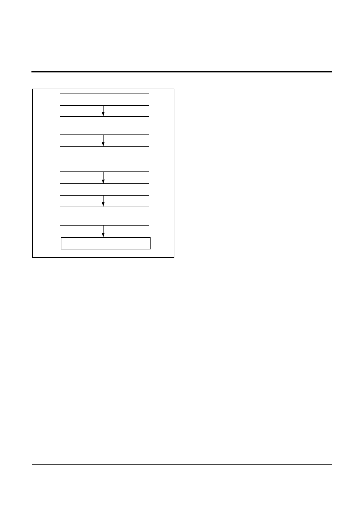
The basic sequence is illustrated in Figure 1.
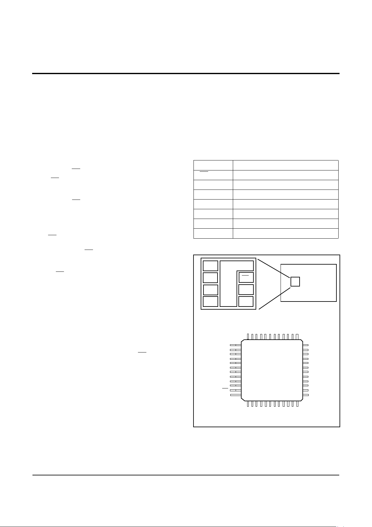
PIN NAMES
PIN CONFIGURATION
After each transaction is completed, the X76F128 will
reset and enter into a standby mode. This will also be the
response if an unsuccessful attempt is made to access a
protected array.
Symbol Description
CS Chip Select Input
SDA Serial Data Input/Output
SCL Serial Clock Input
RST Reset Input
Vcc Supply Voltage
Vss Ground
NC No Connect
V
CC
RST
SCL
NC
SDA
Smart Card
CS
NC
7052 FM 02
GND
1
2
3
4
5
6
7
8
9
10
11
12
36
35
34
33
32
31
30
29
28
27
26
25
1314151617181920212223
24
4847464544434241403938
37
NCNCNCNCNCNCNCNCNCNCNC
NC
VCC
NC
NC
NC
NC
NC
NC
NC
NC
NC
RST
SCL
VSS
NC
NC
NC
NC
NC
NC
NC
NC
NC
CS
SDA
NCNCNCNCNCNCNCNCNCNCNC
NC
7052 FM T01
Page 3
X76F128
3
Figure 1. X76F128 Device Operation
Retry Counter
The X76F128 contains a retry counter. The retry counter
allows 8 accesses with an invalid password before any
action is taken. The counter will increment with any combination of incorrect passwords. If the retry counter overflows, all memory areas are cleared and the device is
locked by preventing any read or write array password
matches. The passwords are unaffected. If a correct
password is received prior to retry counter overflow, the
retry counter is reset and access is granted. In order to
reset the operation of a locked up device, a special reset
command must be used with a RESET PASSWORD.
Device Protocol
The X76F128 supports a bidirectional bus oriented protocol. The protocol defines any device that sends data
onto the bus as a transmitter and the receiving device as
a receiver. The device controlling the transfer is a master
and the device being controlled is the slave. The master
will always initiate data transf ers and pro vide the clock f or
both transmit and receive operations. Therefore, the
X76F128 will be considered a slave in all applications.
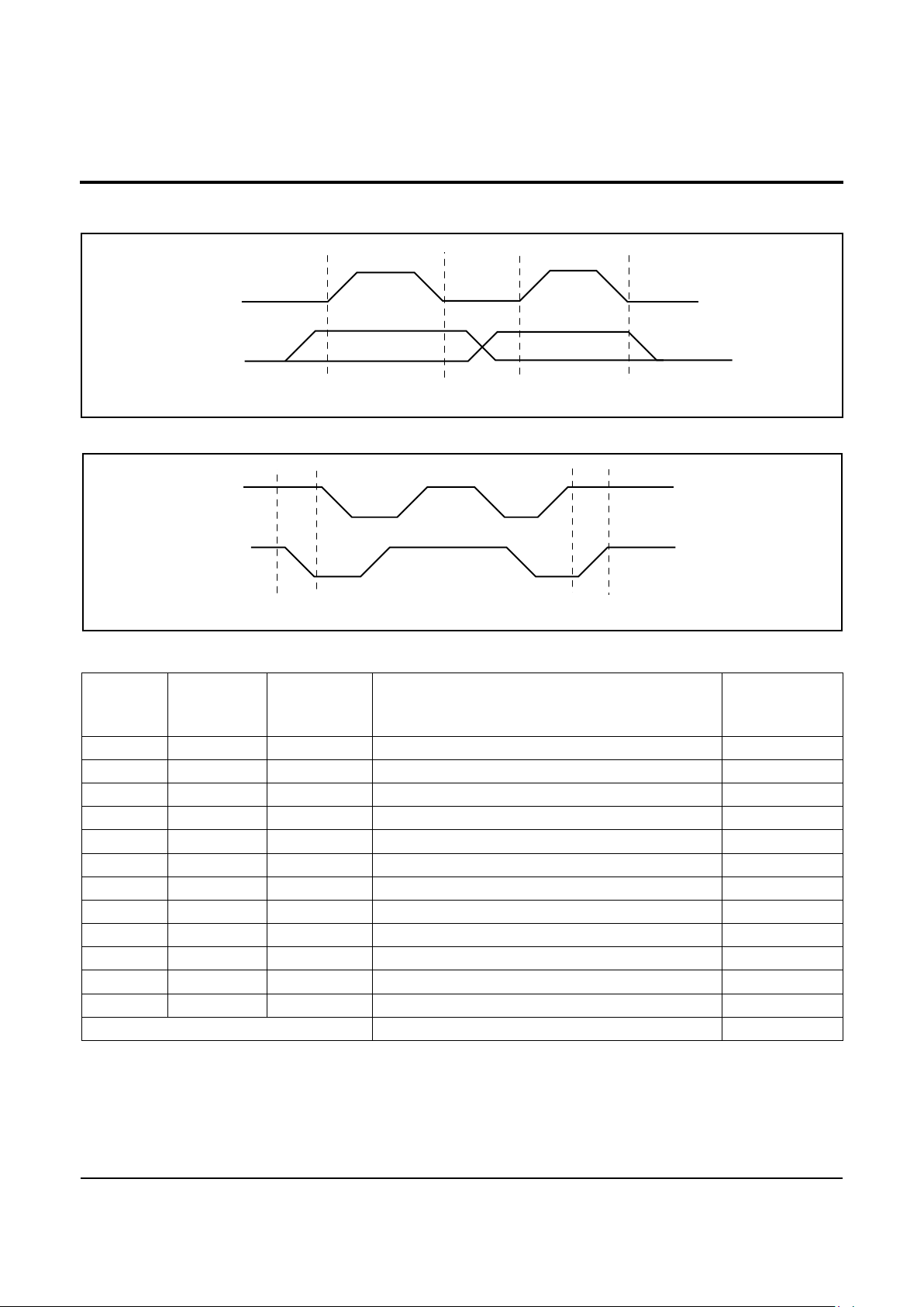
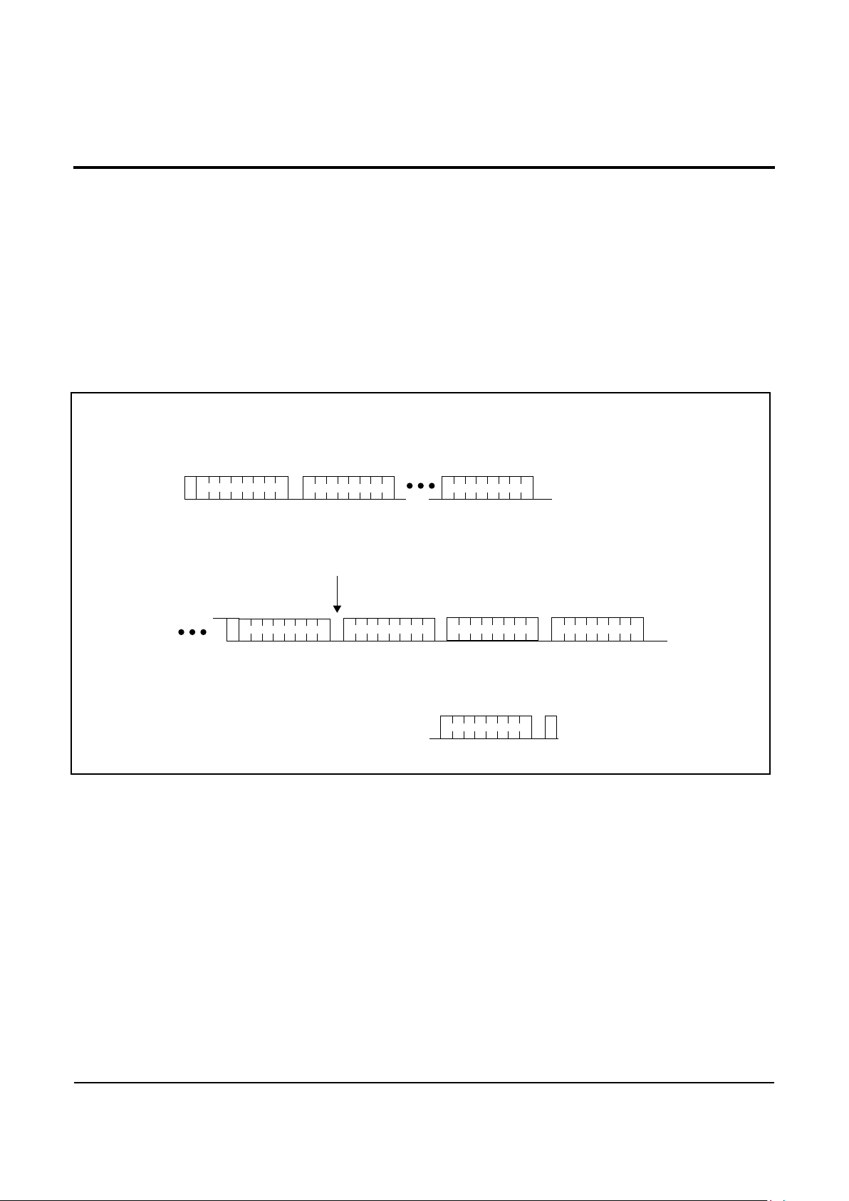
Clock and Data Conventions
Data states on the SDA line can change only during SCL
LOW. SDA changes during SCL HIGH are reserved for
indicating start and stop conditions. Refer to Figure 2 and
Figure 3.
Start Condition
All commands are preceeded by the start condition,
which is a HIGH to LOW transition of SDA when SCL is
HIGH. The X76F128 continuously monitors the SDA and
SCL lines for the start condition and will not respond to
any command until this condition is met.
A start may be issued to terminate the input of a control
byte or the input data to be written. This will reset the
device and leave it ready to begin a new read or write
command. Because of the push/pull output, a start cannot be generated while the part is outputting data. Starts
are inhibited while a write is in progress.
Stop Condition
All communications must be terminated by a stop condition. The stop condition is a LOW to HIGH transition of
SDA when SCL is HIGH. The stop condition is also used
to reset the device during a command or data input
sequence and will leave the device in the standby power
mode. As with starts, stops are inhibited when outputting
data and while a write is in progress.
Acknowledge
Acknowledge is a software convention used to indicate
successful data transfer. The transmitting device, either
master or slave, will release the bus after transmitting
eight bits. During the ninth clock cycle the receiver will
pull the SDA line LOW to acknowledge that it received
the eight bits of data.
The X76F128 will respond with an acknowledge after
recognition of a start condition and its slave address. If
both the device and a write condition have been
selected, the X76F128 will respond with an acknowledge
after the receipt of each subsequent eight-bit word.
RESET DEVICE Command
The RESET DEVICE command is used to clear the retry
counter and reactivate the device. When the RESET
DEVICE command is used prior to the retry counter
overflow, the retry counter is reset and no arrays or passwords are affected. If the retry counter has ov erflowed, all
memory areas are cleared and all commands are
blocked and the retry counter is disabled. Issuing a valid
RESET DEVICE command (with reset password) to the
device resets and re-enables the retry counter and reenables the other commands. Again, the passwords are
not affected.
RESET PASSWORD Command
A RESET PASSWORD command will clear both arrays
and set all passwords to all zero .
LOAD COMMAND BYTE
LOAD 2 BYTE ADDRESS
LOAD 8-BYTE
PASSWORD
VERIFY PASSWORD
ACCEPTANCE BY
USE OF PASSWORD ACK POLLING
READ/WRITE
DATA BYTES
7052 FM 03
Twc OR DATA ACK POLLING
Page 4
X76F128
4
Figure 2. Data Validity
Figure 3. Definition of Start and Stop Conditions
Table 1. X76F128 Instruction Set
Notes: Illegal command codes will be disregarded. The part will respond with a “no-ACK” to the illegal b yte and then return to the standby mode.
All write/read operations require a password.
1st Byte
after Start
1st Byte
after
Password
2nd Byte
after
Password Command Description
Password
used
1000 0000 High Address Low address Read (Array 0) Read 0
1000 1000 High Address Low address Read (Array 1) Read 1
1001 0000 High Address Low address Sector Write (Array 0) Write 0
1001 1000 High Address Low address Sector Write (Array 1) Write 1
1010 0000 0000 0000 0000 0000 Change Read 0 Password Read 0
1010 1000 0000 0000 0000 0000 Change Read 1 Password Read 1
1011 0000 0000 0000 0000 0000 Change Write 0 Password Write 0
1011 1000 0000 0000 0000 0000 Change Write 1 Password Write 1
1100 0000 0000 0000 0000 0000 Change Reset Password Reset
1110 0000 not used not used RESET PASSWORD Command Reset
1110 1000 not used not used RESET DEVICE Command Reset
1111 0000 not used not used ACK Polling command (Ends Password operation) None
All the rest Reserved
SCL
SDA
Data Stable
Data
Change
7052 FM 04
SCL
SDA
Start Condition Stop Condition
7052 FM 05
7052 FM T04
Page 5
X76F128
5
PROGRAM OPERATIONS
Sector Programming
The sector program mode requires issuing the 8-bit write
command followed b y the pass word, pass w ord Ack command, the address and then the data bytes transferred
as illustrated in figure 4. Up to 64 bytes may be transferred. After the last byte to be transferred is acknowledged a stop condition is issued which starts the
nonvolatile write cycle.
Figure 4. Sector Programming
Data 63
ACK
ACK
S
START
COMMAND
ACK
ACK
ACK
ACK
ACK
ACK
A15
A14
A13
A12
A11
A10A9A8
A7A6A5A4A3A2A1
A0
Write
Password
7
Write
Password
0
ACK
Data 0
S
SDA
Wait t
WC
Data ACK Polling
. . .
Wait t
WC
OR
STOP
ACK POLLING
ACK
S
ACK Polling
Repeated
COMMAND
Command
NACK
If ACK, Then
Password Matches
7052 FM 07
START
Page 6
X76F128
6
ACK Polling
Once a stop condition is issued to indicate the end of the
host’s write sequence, the X76F128 initiates the internal
nonvolatile write cycle. In order to take advantage of the
typical 5ms write cycle, ACK polling can begin
immediately. This involves issuing the start condition
followed by the new command code of 8 bits (1st byte of
the protocol.) If the X76F128 is still busy with the
nonvolatile write operation, it will issue a “no-ACK” in
response. If the nonvolatile write operation has
completed, an “ACK” will be returned and the host can
then proceed with the rest of the protocol.
After the password sequence, there is always a nonvolatile write cycle. This is done to discourage random
guesses of the password if the device is being tampered
with. In order to continue the transaction, the X76F128
requires the master to perform an ACK polling with the
specific code of F0h. As with regular Acknowledge polling
the user can either time out for 10ms, and then issue the
ACK polling once, or continuously loop as described in the
flow .
If the password that was inserted was correct, then an
“ACK” will be returned once the nonvolatile cycle is over,
in response to the ACK polling cycle immediately follo wing
it.
If the password that was inserted was incorrect, then a “no
ACK” will be returned even if the nonvolatile cycle is over.
Therefore, the user cannot be certain that the password is
incorrect until the 10ms write cycle time has elapsed.
Data ACK Polling Sequence
ACK
RETURNED?
ISSUE NEW
COMMAND
CODE
WRITE SEQUENCE
COMPLETED
ENTER ACK POLLING
ISSUE START
NO
YES
PROCEED
7052 FM 08
Password ACK Polling Sequence
ACK
RETURNED?
ISSUE
PASSWORD
ACK COMMAND
PASSWORD LOAD
COMPLETED
ENTER ACK POLLING
ISSUE START
NO
YES
PROCEED
7052 FM 09
Figure 5. Acknowledge Polling
8th clk.
of 8th
pwd. byte
‘ACK’
clk
8th
clk
‘ACK’
clk
‘ACK’
START
condition
8th bit
ACK or
no ACK
SCL
SDA
7052 FM 10
Page 7

X76F128
7
READ OPERATIONS
Read operations are initiated in the same manner as write
operations but with a different command code .
Random Read
The master issues the start condition and a Read instruction and password, perf orms a Password Ack Polling, then
issues the word address. Once the password has been
acknowledged and first byte has been read, another start
can be issued followed by a new 8-bit address. Random
reads are allowed, but only the low order 8 bits can
change. This limits random reads to a 512 byte block.
Therefore, with a single password cycle only a 512 byte
block of array 0 may be accessed randomly. To randomly
access another block of arra y 0, a stop m ust be issued f ollowed by a new command/address/pass w ord sequence. A
random read of the array 1 can access all locations without another password command sequence.
Sequential Read
The host can read sequentially within an array after the
password acceptance sequence. The data output is
sequential, with the data from address n followed by the
data from n+1. The address counter for read operations
increments all address bits, allowing the entire memory
array contents to be serially read during one operation. At
the end of the address space (address 3FFFh for array 0,
3Fh for array 1), the counter “rolls over” to address 0 and
the X76F128 continues to output data for each acknowledge received. Refer to figure 7 for the address, acknowledge and data transfer sequence. An acknowledge must
follow each 8-bit data transfer. After the last bit has been
read, a stop condition is generated without a preceding
acknowledge.
Figure 6. Random Read
S
ACK
STOP
A7A6A5A4A3A2A1
A0
Data Y
S
START
START
COMMAND
ACK
ACK
ACK
ACK
Read
Password
7
Read
Password
0
S
SDA
ACK
ACK
A15
A14
A13
A12
A11
A10A9A8
A7A6A5A4A3A2A1
A0
Data X
Wait t
WC
OR
START
ACK POLLING
ACK
S
ACK Polling
Repeated
COMMAND
Command
NACK
If ACK, then
Password Matches
7052 FM 11
Figure 7. Sequential Read
Data X
ACK
S
START
COMMAND
ACK
ACK
ACK
ACK
Read
Password
7
Read
Password
0
S
SDA
ACK
ACK
A15
A14
A13
A12
A11
A10A9A8
A7A6A5A4A3A2A1
A0
ACK
Data 0
If ACK, then
Wait t
WC
OR
START
ACK POLLING
ACK
S
ACK Polling
Repeated
COMMAND
Command
NACK
Password Matches
STOP
7052 FM 12
Page 8

X76F128
8
PASSWORDS
The sequence in Figure 8 shows how to change (program) the passwords. The programming of passwords is
done twice prior to the nonvolatile write cycle in order to
verify that the new password is consistent. After the eight
bytes are entered in the second pass, a comparison
takes place. A mismatch will cause the part to reset and
enter into the standby mode.
Data ACK polling can be used to determine if a password
has been loaded correctly, however the data ACK command must be issued less than 2ms after the stop bit.
After this time, it cannot be determined if the password
has been loaded correctly, without trying the new password. To determine if the new password has been loaded
correctly the data ACK polling command is issued immediately following the stop bit. If it returns an ACK, then the
two passes of the new password entry do not match. If it
returns a "no ACK" then the passwords match and a high
voltage cycle is in progress. The high voltage cycle is
complete when a subsequent data ACK command
returns an "ACK".
There is no way to read any of the passw ords.
Figure 8. Change Passwords
START
COMMAND
ACK
ACK
ACK
ACK
Old
Password
7
Old
Password
0
S
SDA
ACK
ACK
ACK
New
Password
7
Password
0
ACK
ACK
ACK
New
Password
7
New
Password
0
ACK
S
STOP
If ACK, then
ACK
Two bytes of “0”
Wait t
WC
OR
START
ACK POLLING
ACK
S
ACK Polling
Repeated
COMMAND
Command
NACK
Password Matches
If immediate ACK,
then New Password error
Data ACK
Polling
If immediate NACK,
then New Password OK
followed by ACK after ~5ms
7052 FM 13
RESPONSE TO RESET
The X76F128 returns a unique 32 bits response to reset
by implementing the following procedures:
• CS
goes LOW
• RST goes HIGH
• SCK toggles Low-HIGH-Low
• RST goes LOW
• Each subsequent clock forces next response to
reset bit onto SO pin.
For the X76F128, the 32 bit sequence is 19h, 28h, AAh,
55h with each byte output LSB first. See Figure 11.
Page 9

X76F128
9
Figure 9. Reset Password
Figure 10. Reset Device
Figure 11. Response to RESET (RST)
START
Reset Password
ACK
ACK
ACK
ACK
Reset
Password
7
Reset
Password
0
S
SDA
Wait t
WC
OR
START
ACK POLLING
ACK
S
ACK Polling
Repeated
COMMAND
Command
NACK
STOP
S
If ACK, then
Device reset
COMMAND
7052 FM 14
START
Reset Device
ACK
ACK
ACK
ACK
Reset
Password
7
Reset
Password
0
S
SDA
Wait t
WC
OR
START
ACK POLLING
ACK
S
ACK Polling
Repeated
COMMAND
Command
NACK
STOP
S
If ACK, then
Device reset
COMMAND
7052 FM 15
3 2 2
CS
SCK
SO
2 1 1 1 1
8
7 5 3 1
1 8 7 0 8 4 2 0
RST
7052 FM 16
"19" "SS""28"
"AA"
LSB
LSB
LSB
LSB
ABSOLUTE MAXIMUM RATINGS*
Temperature under Bias ......................–65 ° C to +135 ° C
Storage T emperature ...........................–65 ° C to +150 ° C
V oltage on any Pin with
Respect to V
SS
......................................–1V to +7V
D .C. Output Current..................................................5mA
Lead Temperature
(Soldering, 10 seconds).................................300 ° C
*COMMENT
Stresses above those listed under “Absolute Maximum
Ratings” may cause permanent damage to the device.
This is a stress rating only and the functional operation of
the device at these or any other conditions above those
listed in the operational sections of this specification is
not implied. Exposure to absolute maxim um rating conditions for extended periods ma y affect de vice reliability.
Page 10

X76F128
10
RECOMMENDED OPERATING CONDITIONS
7052 FM T05 7052 FM T06
Temp Min. Max.
Commercial 0 ° C +70 ° C
Extended –20
°
C +85 ° C
Supply Voltage Limits
X76F128 4.5V to 5.5V
X76F128 – 2.7 2.7V to 3.6V
D.C. OPERATING CHARACTERISTICS (Over the recommended operating conditions unless otherwise specified.)
7052 FM T07
CAPACITANCE T
A
= +25 ° C, f = 1MHz, V
CC
= 5V
7052 FM T08
NOTES: (1) Must perform a stop command after a read command prior to measurement
(2) V
IL
min. and V
IH
max. are f or reference only and are not tested.
(3) This parameter is periodically sampled and not 100% tested.
Symbol Parameter
Limits
Units Test ConditionsMin. Max.
I
CC1
V
CC
Supply Current
(Read)
1 mA
f
SCL
= V
CC
x 0.1/V
CC
x 0.9 Levels @ 400 KHz,
SDA = Open
RST = CS
= V
SS
I
CC2
(3)
V
CC
Supply Current
(Write)
3 mA
f
SCL
= V
CC
x 0.1/V
CC
x 0.9 Levels @ 400 KHz,
SDA = Open
RST = CS
= V
SS
I
SB1
(1)
VCC Supply Current
(Standby)
50 µA
V
IL
= VCC x 0.1, VIH = VCC x 0.9
f
SCL
= 400 KHz, f
SDA
= 400 KHz
I
SB2
(1)
VCC Supply Current
(Standby)
1 µA
V
SDA
= V
SCC
= V
CC
Other = GND or VCC–0.3V
I
LI
Input Leakage Current 10 µA
V
IN
= VSS to VCC
I
LO
Output Leakage Current 10 µA
V
OUT
= VSS to V
CC
V
IL1
(2)
Input LOW Voltage –0.5
V
CC
x 0.3
V
VCC = 5.5V
V
IH1
(2)
Input HIGH Voltage
V
CC
x 0.7 VCC + 0.5
V
VCC = 5.5V
V
IL2
(2)
Input LOW Voltage –0.5
V
CC
x 0.1
V
VCC = 3.0V
V
IH2
(2)
Input HIGH Voltage
V
CC
x 0.9 VCC + 0.5
V
VCC = 3.0V
V
OL
Output LOW Voltage 0.4 V
I
OL
= 3mA
Symbol Test Max. Units Conditions
C
OUT
(3)
Output Capacitance (SDA) 8 pF
V
I/O
= 0V
C
IN
(3)
Input Capacitance (RST, SCL, CS) 6 pF
V
IN
= 0V
EQUIVALENT A.C. LOAD CIRCUIT A.C. TEST CONDITIONS
7052 FM T09
3V
1.3KΩ
OUTPUT
100pF
5V
1533Ω
OUTPUT
100pF
7052 FM 17
Input Pulse Levels
V
CC
x 0.1 to VCC x 0.9
Input Rise and Fall Times 10ns
Input and Output Timing Level
V
CC
x 0.5
Output Load 100pF
Page 11

X76F128
11
AC CHARACTERISTICS
AC Specifications (Over the recommended operating conditions)
Notes: 1. Typical values are for TA = 25˚C and VCC = 5.0V
Notes: 2. Cb = Total Capacitance of one bus line in pf.
Symbol Parameter Min Typ
(1)
Max Units
f
SCL
SCL Clock Frequency, X76F128 0 400 KHz
f
SCL
SCH Clock Frequency, X76F128–2.7 0 250 KHz
t
IN
(1)
Pulse width of spikes which must be suppressed by
the input filter
50 100 ns
t
AA
SCL LOW to SDA Data Out Valid 0.1 0.3 0.9 µs
t
BUF
Time the bus must be free before a new transmit
can start
1.3 µs
t
LOW
Clock LOW Time 1.3 µs
t
HIGH
Clock HIGH Time 0.6 µs
t
SU:STA
Start Condition Setup Time 0.6 µs
t
HD:STA
Start Condition Hold Time 0.6 µs
t
SU:DAT
Data In Setup Time 100 ns
t
HD:DAT
Data In Hold Time 0 µs
t
SU:STO
Stop Condition Setup Time 0.6 µs
t
DH
Data Output Hold Time 50 300 ns
t
R
SDA and SCL Rise Time
20 + 0.1 x C
b
(2)
300 ns
t
F
SDA and SCL Fall Time
20 + 0.1 x C
b
(2)
300 ns
t
SU:CS
CS Setup Time 200 ns
t
HD:CS
CS Hold Time 100 ns
f
SCL_RST
SCL Clock Frequency during Response to Reset 400 kHz
t
SR
Device Select to RST active 200 ns
t
NOL
RST to SCL Non-Overlap 500 ns
t
RST
RST High Time 2.25 µs
t
SU:RST
Response to Reset Setup Time 1.25 µs
t
LOW_RST
Clock LOW during Response to Reset 1.25 µs
t
HIGH_RST
Clock HIGH during Response to Reset 1.25 µs
t
RDV
RST LOW to SDA Valid During Response to Reset 0 500 ns
t
CDV
CLK LOW to SDA Valid During Response to Reset 0 500 ns
t
DHZ
Device Deselect to SDA high impedance 0 500 ns
7052 FM T14
Page 12

X76F128
12
RESET AC SPECIFICATIONS
Power Up Timing
Notes: 1. Delays are measured from the time VCC is stable until the specified operation can be initiated. These parameters are periodically sampled
and not 100% tested.
2. T ypical values are f or TA = 25˚C and VCC = 5.0V
Nonvolatile Write Cycle Timing
Notes: 1. tWC is the time from a valid stop condition at the end of a write sequence to the end of the self-timed internal nonvolatile write cycle.
It is the minimum cycle time to be allowed for any non volatile write by the user, unless Acknowledge P olling is used.
TIMING DIAGRAMS
Bus Timing
Write Cycle Timing
Symbol Parameter Min. Typ
(2)
Max. Units
t
PUR
(1)
Time from Power Up to Read 1 mS
t
PUW
(1)
Time from Power Up to Write 5 mS
Symbol Parameter Min. Typ.(1) Max. Units
t
WC
(1)
Write Cycle Time 5 10 mS
t
SU:STO
t
DH
t
HIGH
t
SU:STA
t
HD:STA
t
HD:DAT
t
SU:DAT
SCL
SDA IN
SDA OUT
t
F
t
LOW
t
BUF
t
AA
t
R
7052 FM 18
SCL
SDA
t
WC
8th bit of last byte ACK
Stop
Condition
Start
Condition
7052 FM 19
7052 FM T11
7052 FM T12
Page 13

X76F128
13
CS Timing Diagram (Selecting/Deselecting the Part)
RST Timing Diagram – Response to a Synchronous Reset
GUIDELINES FOR CALCULATING TYPICAL VALUES OF BUS PULL UP RESISTORS
t
SU:CS
t
HD:CS
SCL
CS
from
master
7052 FM 20
t
RST
t
NOL
t
HIGH_RST
t
LOW_RST
t
CDV
t
RDV
t
SU:RST
DATA BIT (1)
DATA BIT (2)
1st
clk
pulse
2nd
clk
pulse
3rd
clk
pulse
CS
I/O
CLK
RST
t
NOL
t
SR
DATA BIT (N)
DATA BIT (N+1)
CS
I/O
CLK
RST
t
DHZ
(N+2)
7052 FM 21
10080604020
Bus capacitance in pF
Pull Up Resistance in KΩ
R
MIN
R
MAX
20
40
60
80
100
R
MIN
V
CCMAX
I
OLMIN
-------------------------- 1.8
K
Ω= =
R
MAX
t
R
C
BUS
------------------=
tR = maximum allowable SDA rise time
7052 FM 22
Page 14

X76F128
14
PACKAGING INFORMATION
A2
A1
L
L1
GAGE PLANE 0.25
C
7°±0°
7052 FM 23
He
D
e
b
Hd
E
NOTES:
1.GAGE PLANE DIMENSION IS IN MM.
2.LEAD COPLANARITY SHALL BE 0.10MM [0.004] MAXIMUM.
48-LEAD THIN QUAD FLAT PACK (TQFP) PACKAGE TYPE L
PIN 1
DIM
INCHESMILLIMETERS
MIN MAX MIN MAX
A
1
A
2
b
c
D
E
e
Hd
He
L
L
1
0.05
1.35
0.17
0.090
7.0 BSC
9.0 BSC
0.45
0.15
1.45
0.27
0.200
0.75
0.002
0.53
0.007
0.004
0.018
0.006
0.057
0.011
0.008
0.030
1.00TYP
0.039TYP
0.5 BSC 0.02 BSC
3. MOLD FLASH NOT INCLUDED IN DIMENSIONS
9.0 BSC
0.35 BSC
0.35 BSC
7.0 BSC
0.273 BSC
0.273 BSC
Page 15

X76F128
15
8 PAD CHIP ON BOARD SMART CARD MODULE TYPE X
0.465 ± 0.002
(11.81 ± 0.05)
A
SECTION A-A
A
R. 0.039 (1.00) (4X)
0.285 (7.24) MAX.
0.420 ± 0.002
(10.67 ± 0.05)
0.210 ± 0.002
(5.33 ± 0.05)
0.105 ± 0.002
(2.67 ± 0.05)
TYP.
(8x)
(8x)
0.105 ± 0.002
(2.67 ± 0.05)
0.008 ± 0.001
(0.20 ± 0.03)
0.233 ± 0.002
(5.92 ± 0.05)
0.174 ± 0.002
(4.42 ± 0.05)
0.146 ± 0.002
(3.71 ± 0.05)
DIE
0.0235 (0.60) MAX.
0.015 (0.38) MAX.
0.008 (0.20) MAX.
GLOB SIZE
FR4 TAPE
COPPER, NICKEL PLATED, GOLD FLASH
R. 0.013 (0.33) (8x)
0.270 (6.86) MAX.
0.069 (1.75) MIN EPOXY
FREE AREA (TYP.)
0.088 (2.24) MIN EPOXY
FREE AREA (TYP.)
NOTE:
1. ALL DIMENSIONS IN INCHES AND (MILLIMETERS)
3003 ILL 03.1
Page 16

X76F128
16
3.369 ± 0.002
(85.57 ± 0.05)
2.125 ± 0.002
(53.98 ± 0.05)
0.593 ± 0.002
(15.06 ± 0.05)
3° MAX.
DRAFT ANGLE
(ALL AROUND)
NOTES:
1.ALL DIMENSIONS ARE IN INCHES AND (MILLIMETERS).
2.SPECIFIED DIMS ARE MEASURED AT BOTTOM OF CAVITY.
3.MATERIAL: WHITE PVC MOLDED PLASTIC WITH ANTI-STATIC ADDITIVE.
4.SURFACE FINISH SUITABLE FOR OFFSET PRINTING.
0.430 ± 0.002
(10.92 ± 0.05)
0.475 ± 0.010
(12.07 ± 0.25)
0.478 ± 0.002
(12.14 ± 0.05)
R.0.125
(3.18) (4x)
0.31 ± 0.0005
(.079 ± 0.0127)
SCALE:5x
A
A
R. 0.030 (0.76) (4x)
MOLD GATE DETAIL
SECTION A-A
SMART CARD TYPE Y
3003 ILL 02.1
Page 17

X76F128
17
ORDERING INFORMATION
VCC Limits
Blank = 5V ±10%
2.7 = 2.7V to 3.6V
Temperature Range
Blank = Commercial = 0°C to +70°C
E = Extended = –20°C to +85°C
Package
L = 48-Lead TQFP
H = Die in Waffle Packs
W = Die in Wafer Form
X = Smart Card Module
Y = Smart Card
Device
X76F128 X X –X
LIMITED WARRANTY
Devices sold by Xicor, Inc. are covered by the warranty and patent indemnification provisions appearing in its Terms of Sale only. Xicor, Inc. makes no warranty,
express, statutory, implied, or by description regarding the information set forth herein or regarding the freedom of the described devices from patent infringement.
Xicor, Inc. makes no warranty of merchantability or fitness for any purpose. Xicor, Inc. reserves the right to discontinue production and change specifications and
prices at any time and without notice.
Xicor, Inc. assumes no responsibility f or the use of any circuitry other than circuitry embodied in a Xicor, Inc. product. No other circuits, patents , licenses are implied.
U.S. PATENTS
Xicor products are covered by one or more of the following U.S. Patents: 4,263,664; 4,274,012; 4,300,212; 4,314,265; 4,326,134; 4,393,481; 4,404,475;
4,450,402; 4,486,769; 4,488,060; 4,520,461; 4,533,846; 4,599,706; 4,617,652; 4,668,932; 4,752,912; 4,829, 482; 4,874, 967; 4,883, 976. Foreign patents and
additional patents pending.
LIFE RELATED POLICY
In situations where semiconductor component failure may endanger life, system designers using this product should design the system with appropriate error detection and correction, redundancy and back-up features to prev ent such an occurence.
Xicor’s products are not authorized for use in critical components in life support devices or systems.
1. Life support devices or systems are devices or systems which, (a) are intended for surgical implant into the body, or (b) support or sustain life, and whose failure
to perform, when properly used in accordance with instructions for use provided in the labeling, can be reasonably expected to result in a significant injury to the
user.
2. A critical component is any component of a life support device or system whose failure to perform can be reasonably expected to cause the failure of the life sup-
port device or system, or to affect its safety or effectiv eness.
 Loading...