

Page 1
X22C12
1K Bit X22C12 256 x 4
Nonvolatile Static RAM
FEATURES
• High Performance CMOS
—150ns RAM Access Time
• High Reliability
—Store Cycles: 1,000,000
—Data Retention: 100 Years
• Low Power Consumption
—Active: 40mA Max.
—Standby: 100µA Max.
• Infinite Array Recall, RAM Read and Write Cycles
• Nonvolatile Store Inhibit: V
= 3.5V Typical
CC
• Fully TTL and CMOS Compatible
• JEDEC Standard 18-Pin 300-mil DIP
• 100% Compatible with X2212
DESCRIPTION
The X22C12 is a 256 x 4 CMOS NOVRAM featuring a
high-speed static RAM overlaid bit-for-bit with a nonvolatile E2PROM. The NOVRAM design allows data to
be easily transferred from RAM to E2PROM (STORE)
and from E2PROM to RAM (RECALL). The STORE
operation is completed within 5ms or less and the
RECALL is completed within 1µs.
Xicor NOVRAMs are designed for unlimited write operations to the RAM, either RECALLs from E2PROM or
writes from the host. The X22C12 will reliably endure
1,000,000 STORE cycles. Inherent data retention is
greater than 100 years.
—With Timing Enhancements
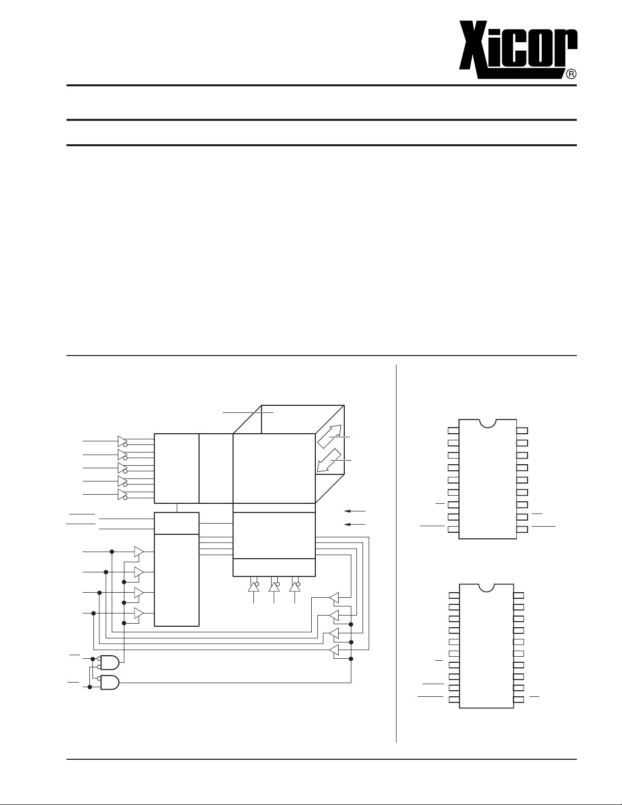
FUNCTIONAL DIAGRAM PIN CONFIGURATION
A
A
A
A
A
A
CS
SS
A7
A
A
A
A
A
CS
SS
7
4
3
2
1
0
4
3
2
1
0
PLASTIC DIP
CERDIP
1
2
3
4
X22C12
5
6
7
8
9
SOIC
X22C12
20
19
18
17
16
15
14
12
1
2
3
4
5
6
7
8
9
10
A
0
A
1
A
2
A
3
A
4
STORE
RECALL
I/O
1
I/O
2
I/O
3
I/O
4
CS
WE
NONVOLATILE E2PROM
MEMORY ARRA Y
ROW
SELECT
CONTROL
LOGIC
INPUT
DATA
CONTROL
STATIC RAM
MEMORY ARRA Y
COLUMN
I/O CIRCUITS
COLUMN SELECT
A7A6A
5
STORE
ARRAY
RECALL
V
V
3817 FHD F01
CC
SS
V
STORE
V
STORE
RECALL
18
17
16
15
14
13
12
11
10
13
11
3815 FHD F10.1
V
CC
A
6
A
5
I/O
4
I/O
3
I/O
2
I/0
1
WE
RECALL
3817 FHD F02
V
CC
A
6
A
5
I/O
4
NC
NC
I/O
3
I/O
2
I/O
1
WE
© Xicor, Inc. 1991, 1995 Patents Pending Characteristics subject to change without notice
3817-2.4 7/30/96 T0/C0/D1 SH
1
Page 2
X22C12
PIN DESCRIPTIONS AND DEVICE OPERATION
Addresses (A0–A7)
The address inputs select a 4-bit memory location
during a read or write operation.
Chip Select (CS)
The Chip Select input must be LOW to enable read or
write operations with the RAM array. CS HIGH will place
the I/O pins in the high impedance state.
Write Enable (WE)
The Write Enable input controls the I/O buffers, determining whether a RAM read or write operation is enabled. When CS is LOW and WE is HIGH, the I/O pins
will output data from the selected RAM address locations. When both CS and WE are LOW, data presented
at the I/O pins will be written to the selected address
location.
Data In/Data Out (I/O1–I/O4)
Data is written to or read from the X22C12 through the
I/O pins. The I/O pins are placed in the high impedance
state when either CS is HIGH or during either a store or
recall operation.
STORE
The STORE input, when LOW, will initiate the transfer of
the entire contents of the RAM array to the E2PROM
array. The WE and RECALL inputs are inhibited during
the store cycle. The store operation is completed in 5ms
or less.
A store operation has priority over RAM read/write
operations. If STORE is asserted during a read operation, the read will be discontinued. If STORE is asserted
during a RAM write operation, the write will be immediately terminated and the store performed. The data at
the RAM address that was being written will be unknown
in both the RAM and E2PROM arrays.
RECALL
The RECALL input, when LOW, will initiate the transfer
of the entire contents of the E2PROM array to the RAM
array. The transfer of data will be completed in 1µs or
less.
An array recall has priority over RAM read/write operations and will terminate both operations when RECALL
is asserted. RECALL LOW will also inhibit the STORE
input.
Automatic Recall
Upon power-up the X22C12 will automatically recall
data from the E2PROM array into the RAM array.
Write Protection
The X22C12 has three write protect features that are
employed to protect the contents of the nonvolatile
memory.
•VCC Sense—All functions are inhibited when VCC is
<3.5V typical.
• Write Inhibit—Holding either STORE HIGH or
RECALL LOW during power-up or power-down will
prevent an inadvertent store operation and E2PROM
data integrity will be maintained.
• Noise Protection—A STORE pulse of typically less
than 20ns will not initiate a store cycle.
PIN NAMES
Symbol Description
A0–A
7
I/O1–I/O
4
Address Inputs
Data Inputs/Outputs
WE Write Enable
CS Chip Select
RECALL Recall
STORE Store
V
CC
V
SS
+5V
Ground
NC No Connect
3817 PGM T01
2
Page 3
X22C12
ABSOLUTE MAXIMUM RATINGS
Temperature under Bias .................. –65°C to +135°C
Storage Temperature ....................... –65°C to +150°C
Voltage on any Pin with
Respect to V
.......................................
SS
–1V to +7V
D.C. Output Current ............................................ 5mA
Lead Temperature
(Soldering, 10 seconds).............................. 300°C
COMMENT
Stresses above those listed under “Absolute Maximum
Ratings” may cause permanent damage to the device.
This is a stress rating only and the functional operation of
the device at these or any other conditions above those
indicated in the operational sections of this specification is
not implied. Exposure to absolute maximum rating conditions for extended periods may affect device reliability.
RECOMMENDED OPERATING CONDITIONS
Temperature Min. Max.
Commercial 0°C +70°C
Industrial –40°C +85°C
Supply Voltage Limits
X22C12 5V ±10%
3817 PGM T13
Military –55°C +125°C
3817 PGM T12.1
D.C. OPERATING CHARACTERISTICS (Over the recommended operating conditions, unless otherwise specified.)
Limits
Symbol Parameter Min. Max. Units Test Conditions
l
CC
VCC Supply Current, 40 mA CS = VIL, I/Os = Open, All Others =
RAM Read/Write VIH, Addresses = 0.4V/2.4V Levels @
f = 8MHz
I
SB1
I
SB2
VCC Standby Current 2 mA Store or Recall Functions Not Active,
(TTL Inputs) I/Os = Open, All Other Inputs = V
V
Standby Current 100 µA Store or Recall functions Not Active,
CC
IH
(CMOS Inputs) I/Os = Open, All Other Inputs =
VCC –0.3V
I
I
V
V
V
V
LI
LO
lL
IH
OL
OH
(2)
(2)
Input Leakage Current 10 µAVIN = VSS to V
Output Leakage Current 10 µAV
= VSS to V
OUT
Input LOW Voltage –1 0.8 V
Input HIGH Voltage 2 VCC + 1 V
Output LOW Voltage 0.4 V IOL = 4.2mA
Output HIGH Voltage 2.4 V IOH = –2mA
CC
CC
3817 PGM T02.3
CAPACITANCE TA = +25°C, f = 1MHz, VCC = 5V
Symbol Parameter Max. Units Test Conditions
(1)
C
I/O
(1)
C
IN
Notes: (1) This parameter is periodically sampled and not 100% tested.
(2) VIL min. and VIH max. are for reference only and are not tested.
Input/Output Capacitance 8 pF V
Input Capacitance 6 pF V
3
I/O
IN
= 0V
= 0V
3815 PGM T03.1
Page 4
X22C12
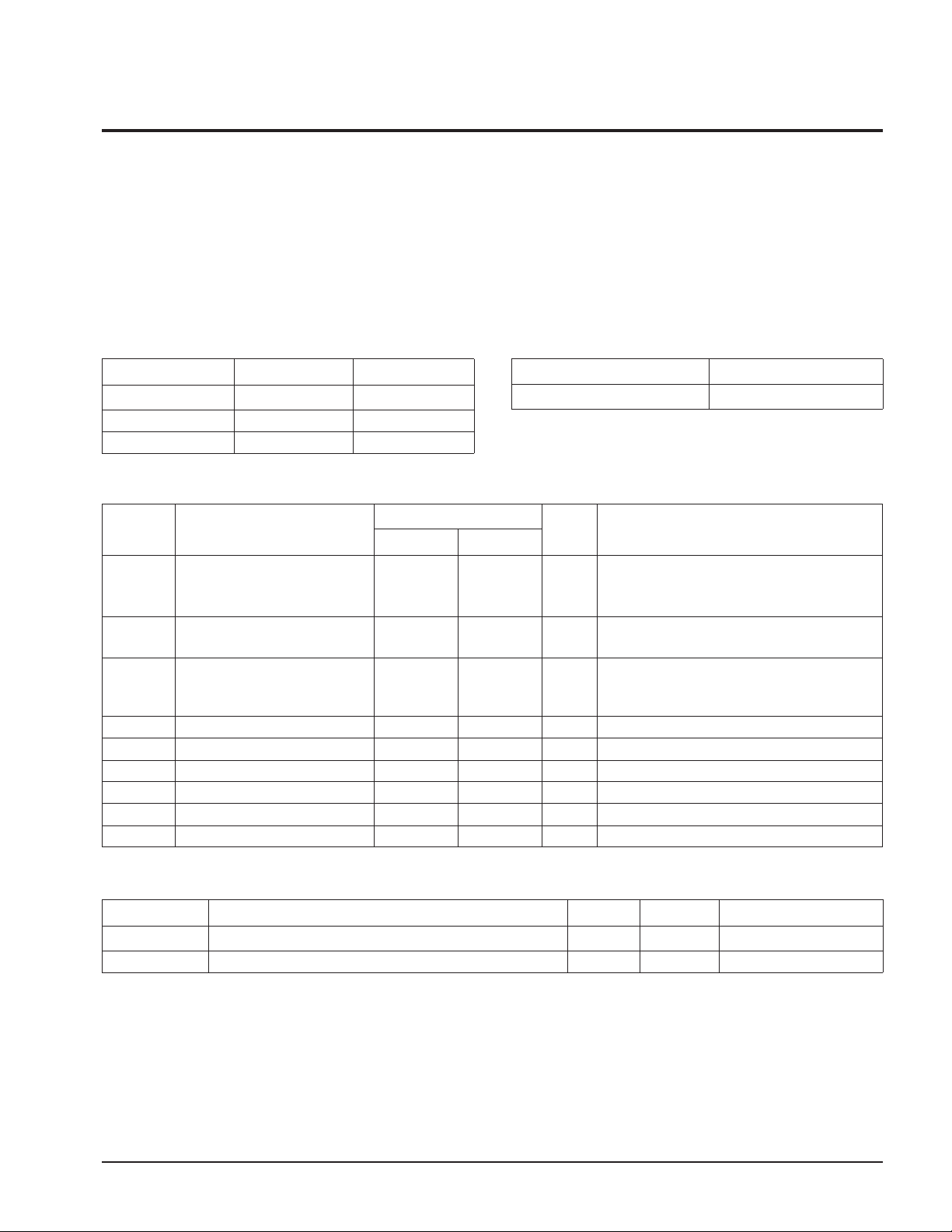
MODE SELECTION
CE WE RECALL STORE I/O Mode
H X H H Output High Z Not Selected
L H H H Output Data Read RAM
L L H H Input Data High Write “1” RAM
L L H H Input Data Low Write “0” RAM
X H L H Output High Z Array Recall
H X L H Output High Z Array Recall
X H H L Output High Z Nonvolatile Store
H X H L Output High Z Nonvolatile Store
ENDURANCE AND DATA RETENTION
Parameter Min. Units
Endurance 100,000 Data Changes Per Bit
Store Cycles 1,000,000 Store Cycles
Data Retention 100 Years
(3)
(4)
(4)
3817 PGM T05.1
3817 PGM T06
POWER-UP TIMING
Symbol Parameter Max. Units
(5)
t
PUR
(5)
t
PUW
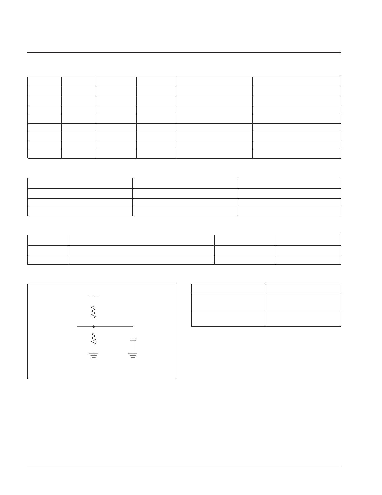
EQUIVALENT A.C. LOAD CIRCUIT
Power-up to Read Operation 100 µs
Power-up to Write or Store Operation 5 ms
A.C. CONDITIONS OF TEST
5V
Input Pulse Levels 0V to 3V
Input Rise and
Fall Times 10ns
919Ω
OUTPUT
497Ω
Notes: (3) Chip is deselected but may be automatically completing a store cycle.
(4) STORE = LOW is required only to initiate the store cycle, after which the store cycle will be automatically completed
(e.g. STORE = X).
(5) t
and t
PUR
parameters are periodically sampled and not 100% tested.
are the delays required from the time VCC is stable until the specified operation can be initiated. These
PUW
100pF
3815 FHD F09.1
Input and Output
Timing Levels 1.5V
3817 PGM T07
3817 PGM T04.1
4
Page 5

X22C12
CS
ADDRESS
t
RC
t
CO
t
A
t
HZ
t
LZ
DATA I/O
t
OH
DATA VALID
A.C. CHARACTERISTICS (Over the recommended operating conditions, unless otherwise specified.)
Read Cycle Limits
Symbol Parameter Min. Max. Units
t
RC
t
AA
t
CO
t
OH
(6)
t
LZ
(6)
t
HZ
Read Cycle
Read Cycle Time 150 ns
Access Time 150 ns
Chip Select to Output Valid 150 ns
Output Hold from Address Change 0 ns
Chip Select to Output in Low Z 0 ns
Chip Deselect to Output in High Z 50 ns
3817 PGM T08
Note: (6) tLZ min. and tHZ min. are periodically sampled and not 100% tested.
3817 FHD F03
5
Page 6

X22C12
Write Cycle Limits
Symbol Parameter Min. Max. Units
t
WC
t
CW
t
AS
t
WP
t
WR
t
DW
t
DH
t
WZ
t
OW
Write Cycle
ADDRESS
CS
WE
DATA IN
Write Cycle Time 150 ns
Chip Select to End of Write 90 ns
Address Setup Time 0 ns
Write Pulse Width 90 ns
Write Recovery Time 0 ns
Data Valid to End of Write 40 ns
Data Hold Time 0 ns
Write Enable to Output in High Z 50 ns
Output Active from End of Write 0 ns
3817 PGM T09.1
t
WC
t
CW
t
AS
t
WP
t
DW
DATA VALID
t
DH
t
WR
DATA OUT
Early Write Cycle
ADDRESS
CS
WE
DATA IN
DATA OUT
t
DH
t
OW
t
3817 FHD F04
WR
3817 FHD F05
t
WZ
t
WC
t
CW
t
AS
HIGH Z
t
WP
t
DW
DATA VALID
6
Page 7

X22C12
Recall Cycle Limits
Symbol Parameter Min. Max. Units
t
RCC
(7)
t
RCP
t
RCZ
t
ORC
t
ARC
Recall Cycle
ADDRESS
RECALL
CS
DATA I/O
Array Recall Time 1 µs
Recall Pulse Width 90 ns
Recall to Output in High Z 50 ns
Output Active from End of Recall 0 ns
Recalled Data Access Time from End of Recall 120 ns
3817 PGM T10
t
RCC
t
RCP
t
RCZ
t
ORC
t
ARC
3817 FHD F06
Note: (7) RECALL rise time must be less than 1µs.
7
Page 8

X22C12
Store Cycle Limits
Symbol Parameter Min. Max. Units
t
STC
t
STP
t
STZ
t
OST
Store Cycle Limits
STORE
DATA I/O
Internal Store Time 5 ms
Store Pulse Width 90 ns
Store to Output in High Z 50 ns
Output Active from End of Store 0 ns
3817 PGM T11
t
STC
t
STP
t
STZ
HI Z
t
OST
3817 FHD F07
SYMBOL TABLE
WAVEFORM
INPUTS
OUTPUTS
Must be
steady
May change
from LOW
to HIGH
May change
from HIGH
to LOW
Don’t Care:
Changes
Allowed
N/A
Will be
steady
Will change
from LOW
to HIGH
Will change
from HIGH
to LOW
Changing:
State Not
Known
Center Line
is High
Impedance
8
Page 9

X22C12
PIN 1 INDEX
18-LEAD PLASTIC DUAL IN-LINE PACKAGE TYPE P
0.915 (23.24)
0.894 (22.71)
0.270 (6.86)
0.250 (6.35)
PIN 1
0.800 (20.32)
REF.
0.060 (1.52)
0.050 (1.27)
SEATING
PLANE
0.140 (3.56)
0.120 (3.05)
0.110 (2.79)
0.090 (2.29)
TYP. 0.010 (0.25)
0.070 (1.78)
0.050 (1.27)
0.325 (8.26)
0.300 (7.62)
0.020 (0.51)
0.016 (0.41)
0°
15°
NOTE:
1. ALL DIMENSIONS IN INCHES (IN PARENTHESES IN MILLIMETERS)
2. PACKAGE DIMENSIONS EXCLUDE MOLDING FLASH
0.165 (4.19)
0.130 (3.30)
0.025 (0.51)
0.005 (0.13)
3926 FHD F02
9
Page 10

X22C12
18-LEAD HERMETIC DUAL IN-LINE PACKAGE TYPE D
0.960 (24.38)
––
0.310 (7.87)
0.220 (5.59)
SEATING
PLANE
0.150 (3.81) MIN.
PIN 1
0.200 (5.08)
0.125 (3.18)
0.110 (2.79)
0.090 (2.29)
TYP. 0.100 (2.54)
0.015 (0.38)
0.008 (0.20)
0.800 (20.32)
REF.
0.065 (1.65)
0.038 (0.97)
TYP. 0.060 (1.52)
0.320 (8.13)
0.290 (7.37)
TYP. 0.311 (7.90)
0.005 (0.13) MIN.
0.098 (2.49)
––
0.200 (5.08)
––
0.070 (1.78)
0.015 (0.38)
0.023 (0.58)
0.014 (0.36)
TYP. 0.018 (0.46)
0°
15°
NOTE: ALL DIMENSIONS IN INCHES (IN PARENTHESES IN MILLIMETERS)
3926 FHD F06
10
Page 11

X22C12
20-LEAD PLASTIC SMALL OUTLINE GULL WING PACKAGE TYPE S
0° – 8°
PIN 1 INDEX
(4X) 7°
0.050 (1.27)
0.010 (0.25)
0.020 (0.50)
PIN 1
0.015 (0.40)
0.050 (1.27)
X 45°
0.014 (0.35)
0.020 (0.50)
0.496 (12.60)
0.508 (12.90)
0.007 (0.18)
0.011 (0.28)
0.420"
0.290 (7.37)
0.299 (7.60)
0.003 (0.10)
0.012 (0.30)
0.050" Typical
0.393 (10.00)
0.420 (10.65)
0.092 (2.35)
0.105 (2.65)
0.050"
Typical
0.030" Typical
FOOTPRINT
20 Places
NOTE: ALL DIMENSIONS IN INCHES (IN PARENTHESES IN MILLIMETERS)
3926 FHD F23
11
Page 12

X22C12
ORDERING INFORMATION
X22C12 X X
Device
Store Cycles
Blank = 1,000,000
Temperature Range
Blank = Commercial = 0°C to +70°C
I = Industrial = –40°C to +85°C
M = Military = –55°C to +125°C
MB = MIL-STD-883
Package
P = 18-Lead Plastic DIP
D = 18-Lead Cerdip
S = 20-Lead Plastic SOIC (300 mil)
LIMITED WARRANTY
Devices sold by Xicor, Inc. are covered by the warranty and patent indemnification provisions appearing in its Terms of Sale only. Xicor, Inc. makes no warranty,
express, statutory, implied, or by description regarding the information set forth herein or regarding the freedom of the described devices from patent infringement.
Xicor, Inc. makes no warranty of merchantability or fitness for any purpose. Xicor, Inc. reserves the right to discontinue production and change specifications and
prices at any time and without notice.
Xicor, Inc. assumes no responsibility for the use of any circuitry other than circuitry embodied in a Xicor, Inc. product. No other circuits, patents, licenses are
implied.
U.S. PATENTS
Xicor products are covered by one or more of the following U.S. Patents: 4,263,664; 4,274,012; 4,300,212; 4,314,265; 4,326,134; 4,393,481; 4,404,475;
4,450,402; 4,486,769; 4,488,060; 4,520,461; 4,533,846; 4,599,706; 4,617,652; 4,668,932; 4,752,912; 4,829, 482; 4,874, 967; 4,883, 976. Foreign patents and
additional patents pending.
LIFE RELATED POLICY
In situations where semiconductor component failure may endanger life, system designers using this product should design the system with appropriate error
detection and correction, redundancy and back-up features to prevent such an occurence.
Xicor’s products are not authorized for use in critical components in life support devices or systems.
1. Life support devices or systems are devices or systems which, (a) are intended for surgical implant into the body, or (b) support or sustain life, and whose
failure to perform, when properly used in accordance with instructions for use provided in the labeling, can be reasonably expected to result in a significant
injury to the user.
2. A critical component is any component of a life support device or system whose failure to perform can be reasonably expected to cause the failure of the life
support device or system, or to affect its safety or effectiveness.
12
 Loading...