

Page 1
®
X00602MA
SENSITIVE 0.8A SCRs
MAIN FEATURES:
Symbol Value Unit
I
T(RMS)
V
DRM/VRRM
I
GT
0.8 A
600 V
200 µA
DESCRIPTION
Thanks to highly sensitive triggering levels, the
X006 SCR series is suitable for all applications
where the available gate current is limited, such as
ground fault circuit interrupters, overvoltage
crowbar protection in low power supplies,
capacitive ignition circuits, ...
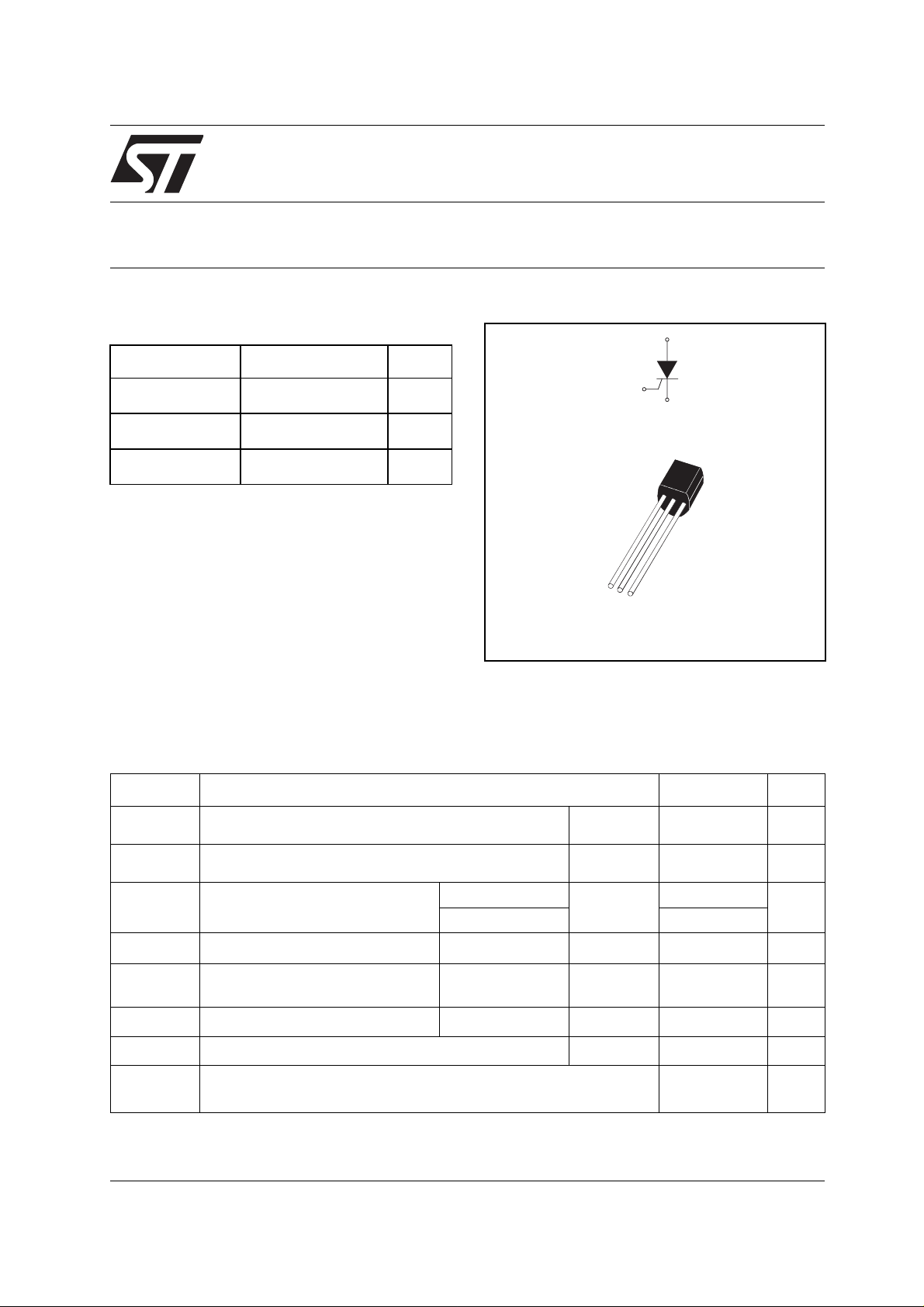
A
G
K
K
G
A
TO-92
ABSOLUTE RATINGS (lim iting values)
Symbol Parameter Value Unit
I
T(RMS)
IT
(AV)
I
TSM
²
I
dI/dt
I
GM
P
G(AV)
T
stg
Tj
January 2002 - Ed: 5
RMS on-state current (180° conduction angle)
Average on-state current (180° conduction angle)
Non repetitive surge peak on-state
current
tI
²
t Value for fusing
Critical rate of rise of on-state current
I
= 2 x IGT , tr ≤ 100 ns
G
tp = 8.3 ms
tp = 10 ms 9
tp = 10ms Tj = 25°C 0.25
F = 60 Hz Tj = 125°C 50 A/µs
Tl = 85°C 0.8
Tl = 85°C 0.5
Tj = 25°C
Peak gate current tp = 20 µs Tj = 125°C 1 A
Average gate power dissipation Tj = 125°C 0.1 W
Storage junction temperature range
Operating junction temp erature range
- 40 to + 125
- 40 to + 125
10
A
A
A
2
S
A
°C
1/5
Page 2
X00602MA
ELECTRICAL CHARACTERISTICS (Tj = 25°C, unless otherwise specified)
Symbol Test Conditions X00602MA Unit
I
GT
VD = 12 V RL = 140 Ω
V
GT
V
V
dV/dt
V
V
I
DRM
I
RRM
VD = V
GD
IRG = 10 µA
RG
I
I
H
I
L
TM
t0
R
= 50 mA RGK = 1 kΩ
T
IG = 1 mA RGK = 1 kΩ
= 67 % V
V
D
ITM = 1 A tp = 380 µs
Threshold voltage Tj = 125°C MAX. 0.85 V
Dynamic resistance Tj = 125°C MAX. 245 mΩ
d
V
DRM
RL = 3.3 kΩ RGK = 1 kΩ
DRM
RGK = 1 kΩ
DRM
= V
RRM
THERMAL RESISTANCES
RGK = 1 kΩ
Tj = 125°C MIN.
Tj = 125°C MIN. 25 V/µs
Tj = 25°C MAX. 1.35 V
Tj = 25°C MAX. 1 µA
Tj = 125°C 100
MIN. 15
MAX. 200 µA
MAX. 0.8 V
0.2 V
MIN.
5V
MAX. 5 mA
MAX. 6 mA
µA
Symbol Parameter Value Unit
R
R
th(j-l)
th(j-a)
Junction to lead (DC)
Junction to ambient (DC)
70
150
PRODUCT SELECTOR
Part Number Voltage Sensitivity Package
X00602MA 600 V 200 µA TO-92
ORDERING INFORMATION
Blank
PACKAGE:
A:TO-92
PACKING MODE:
1AA2: Bulk
2AL2: Ammopack
5AL2:Tape & reel
SENSITIVE
SCR
SERIES
CURRENT:0.8A
X 006 02 M A 1AA2
VOLTAGE:
M: 600V
SENSITIVITY:
02: 200µA
OTHER INFORMATION
°C/W
°C/W
Part Number Marking Weight Base Quantity Packing mode
X00602MA 1AA2 X0602MA 0.2 g 2500 Bulk
X00602MA 2AL2 X0602MA 0.2 g 2000 Ammopack
X00602MA 5AL2 X0602MA 0.2 g 2000 Tape & reel
2/5
Page 3

X00602MA
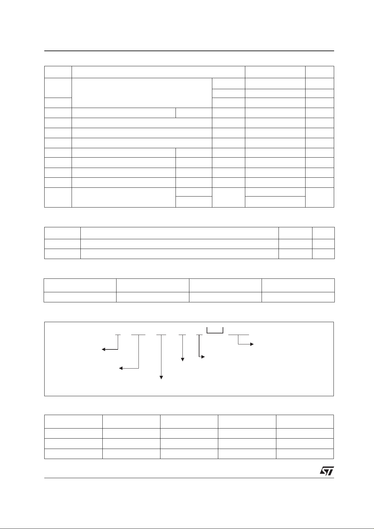
Fig. 1: Maximum average power dissipation
versus average on-state current.
P(W)
0.65
α = 180°
0.60
0.55
0.50
0.45
0.40
0.35
0.30
0.25
0.20
0.15
0.10
0.05
0.00
0.0 0.1 0.2 0.3 0.4 0.5 0.6
IT(av)(A)
360°
α
Fig. 2-2: Average and D.C. on-state current
versus ambient temperature (device mounted o n
FR4 with recommended pad layout).
IT(av)(A)
1.0
0.9
0.8
0.7
0.6
0.5
0.4
0.3
0.2
0.1
0.0
0 25 50 75 100 125
D.C.
α = 180°
Tamb(°C)
Fig. 2-1: Average and D.C. on-state current
versus lead temperature.
IT(av)(A)
1.1
1.0
0.9
0.8
0.7
0.6
0.5
0.4
0.3
0.2
0.1
0.0
0 25 50 75 100 125
D.C.
α = 180°
Tlead(°C)
Fig. 3: Relative variation of thermal impedance
junction to ambient versus pulse duration.
K = [Zth(j-a)/Rth(j-a)]
1.00
0.10
0.01
1E-2 1E-1 1E+0 1E+1 1E+2 5E+2
tp(s)
Fig. 4: Relative variation of gate trigger current,
holding current and latching current versus
junction temperature.
IGT,IH, IL[Tj] / IGT, IH, IL[Tj = 25°C]
1.6
1.4
1.2
1.0
0.8
0.6
0.4
0.2
0.0
-40 -20 0 20 40 60 80 100 120 140
IGT
Tj(°C)
IH & IL
Fig. 5: Relative variation of holding current
versus gate-cathode resistance (typical values).
IH[Rgk]/IH[Rgk=1k ]Ω
3.5
3.0
2.5
2.0
1.5
1.0
0.5
0.0
1E-2 1E-1
Rgk(k )Ω
1E+0
1E+1 1E+2
3/5
Page 4

X00602MA
Fig. 6: Relative variation of dV/dt immunity
versus gate-cathode resistance (typical values).
dV/dt[Rgk]/dV/dt[Rgk=1k ]Ω
1E+2
1E+1
1E+0
1E-1
Rgk(k )Ω
1E-2
1E-2
1E-1 1E+0
1E+1
Fig. 8: Surge peak on-state current versus
number of cycles.
ITSM(A)
10
9
8
7
6
Nonrepetitive
Tjinitial=25°C
5
4
3
Repetitive
T
amb=25°C
2
1
0
1 10 100 1000
tp=10ms
Onecycle
Number of cycles
Fig. 7: Relative variation of dV/dt immunity
versus gate-cathode capacitance (typical
values).
dV/dt[Cgk]/dV/dt[Rgk=1k ]Ω
20
10
5
2
Cgk(nF)
1
12
5
10
Fig. 9: Non-repetitive surge peak on-state
current for a sinusoidal pulse with width
tp < 10 ms, and corresponding value of I²t.
ITSM(A),I2t(A2s)
100.0
ITSM
10.0
1.0
tp(ms)
0.1
0.01 0.10 1.00 10.00
Tj initial = 25°C
I2t
Fig. 10: On-state characteristics (maximum
values).
ITM(A)
1E+1
1E+0
1E-1
1E-2
4/5
Tj max.:
Vto = 0.85V
Rd = 245mΩ
Tj = Tjmax.
Tj = 25°C
VTM(V)
0.5 1.0 1.5 2.0 2.5 3.0 3.5
Page 5

X00602MA
PACKAGE MECHANICAL DAT A
TO-92 (Plastic)
DIMENSIONS
BAC
REF .
a
Millimeters Inches
Min. Typ. Max. Min. Typ. Max.
A 1.35 0.053
B 4.70 0.185
C 2.54 0.100
D 4.40 0.173
F
D
E
E 12.70 0.500
F 3.70 0.146
a 0.50 0.019
Information furnished is believed to be accurate and reliable. However, STMicroelectronics assumes no responsibility for the consequences
of use of su ch in for mat i on n or f or a ny in fr ing em ent of pa te nts or o ther r igh ts of th ir d pa r tie s w hic h may res ul t f rom i ts us e. No license is granted
by impl i cation or otherwise under any patent or patent rights of STMicr oel ectronic s. Specifications mentione d i n this publ i cation are subject
to change wi t hout notice. T hi s publicati on supersedes and replaces all informat i on previou sly supplied. STMicroelectronics product s ar e not
authori zed for use as critical components i n l i fe support devices or systems without express written ap proval of STM i croelectronics.
© The ST logo is a registered trademark of STMicroelectronics
© 2002 STMicroelectronics - Printed in Italy - All Rights Reserved
STMicroele ct ronics GROUP OF C OM P ANIES
Australia - Brazi l - Canada - Ch i na - F i nland - France - Germany
Hong Kong - India - Israel - Italy - Japan - Malaysia - Malta - Morocco - Singapore
Spain - Sweden - Switz erl and - United Kingdom - U ni ted States
http://www.st.com
5/5
 Loading...