

Page 1
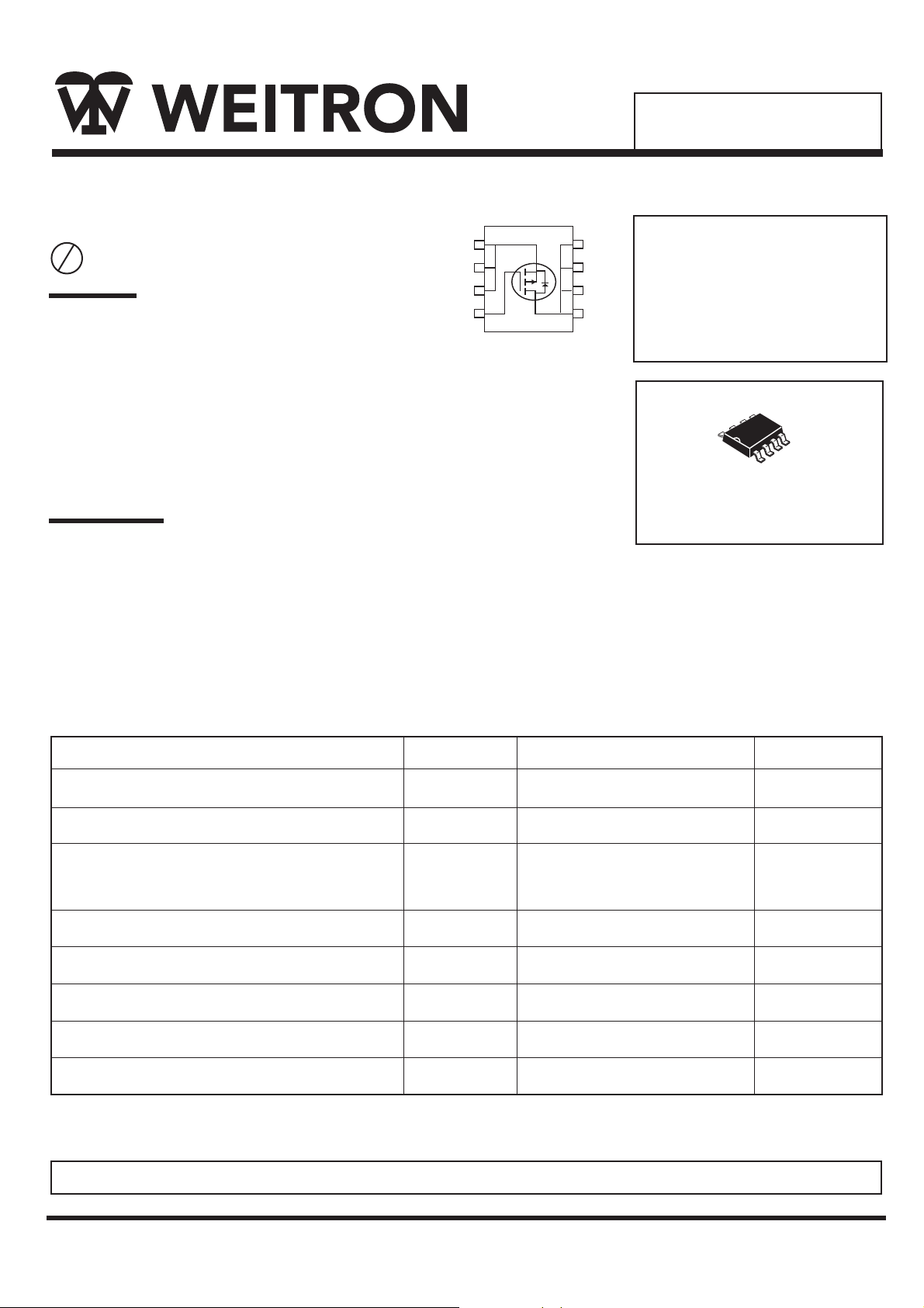
Surface Mount P-Channel
WTK9431
Enhancement Mode MOSFET
1
S S
P b
Lead(Pb)-Free
Features:
2
S
3
G
4
* Super high dense
* Cell design for low RDS(ON)
* R
* R
DS(ON)
DS(ON)
<130mΩ@VGS = -4.5V
<180mΩ@VGS = -2.5V
* Simple Drive Requirement
* Lower On-resistance
* Fast Switching
Description:
The WTK9431 provide the designer with the best combination
of fast switching, ruggedized device design, low on-resistance
and cost-effectiveness.
The SOP-8 package is universally preferred for all commercial-industrial
surface mount applications and suited for low voltage applications such as DC/DC converters.
D
8
D D D
7
6 5
DRAIN CURRENT
-3.5 AMPERES
DRAIN SOURCE VOLTAGE
-20 VOLTAGE
1
SOP-8
Maximum Ratings (T
=25˚C Unless Otherwise Specified)
A
Rating Symbol Value Unite
Drain-Source Voltage
Gate-Source Voltage
Continuous Drain Current
(3)
(TA =25°C)
(TA =70°C)
Pulsed Drain Current
(1,2)
Power Dissipation
Maximax Junction-to-Ambient
Operating Junction Temperature Range
Storage Temperature Range
Device Marking
V
DS
V
GS
I
D
I
DM
P
D
R
θ
T
Tstg
J
JA
-20
±8
-3.5
-2.8
-18
2.5
50
+150
-55 to +150
V
V
A
A
W
°
C/W
°
°
C
C
WTK9431=9431SC
WEITRON
http://www.weitron.com.tw
1/5 07-Nov-08
Page 2
WTK9431
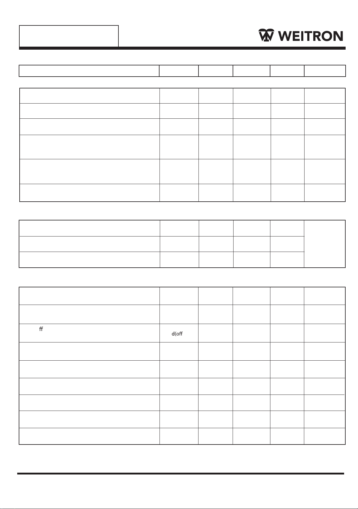
Electrical Characteristics
Characteristic
Static
Drain-Source Breakdown Voltage
VGS=0V, ID=-250 µA
Gate-Source ThresholdVoltage
VDS=VGS, ID=-250 µA
Gate-Source Leakage Current
VDS=0V,VGS= 8V
Zero Gate Voltage Drain Current
VDS=-16V,VGS=0V
VDS=-12V,VGS=0V
Drain-Source On-Resistance
VGS=-10V, ID=-5.3A
=-4.5V, ID=-4.2A
V
GS
orward Transconductance
F
VDS=-5V, ID=-3.5A
+
-
(2)
(2)
Dynamic
Input Capacitance
VDS=-10V,VGS=0V, f=1MHZ
Output Capacitance
VDS=-10V,VGS=0V, f=1MHZ
Reverse Transfer Capacitance
VDS=-10V,VGS=0V, f=1MHZ
(TA=25°C Unless otherwise noted)
Symbol
V
(BR)DSS
V
GS (th)
I
GSS
I
DSS
R
DS(on)
g
fs
C
iss
C
oss
C
rss
Min Typ Max
-20
-0.4 -
-
-
-
-
-
-
-
-
-
-
-
-
-
6.5
405
170
45
+
100
-
-
-1.0
-1
-25
130
180
-
-
-
Unit
V
V
nA
µA
m
Ω
S
F
P
-
Switching
Turn-On Delay Time
VDD= -5V, ID= -1A, VGS= -4.5V, RG= 6Ω
Rise Time
VDD= -5V, ID= -1A, VGS= -4.5V, RG= 6Ω
Turn-O Time
VDD= -5V, ID= -1A, VGS= -4.5V, RG= 6Ω
Fall Time
VDD= -5V, ID= -1A, VGS= -4.5V, RG= 6Ω
Total Gate Charge
VDS=-5V, ID=-5.3A,VGS=-4.5V
Gate-Source Charge
VDS=-5V, ID=-5.3A,VGS=-4.5V
Gate-Drain Charge
VDS=-5V, ID=-5.3A,VGS=-4.5V
Drain-Source
VGS=0V, IS=-2.1A
Continuous Source Current (Body Diode)
VD=VG=0V, VS=-1.2V
Notes:
1. Pulse width limited by Max. junction temperature.
2. Pulse width 300µs, duty cycle ≤ 2%.
3. Surface mounted on 1 in2 copper pad of FR4 board; 125°C/W when mounted on Min. copper pad.
(2)
(2)
Diode Forward Voltage
(2)
t
d(on)
t
t
r
t
f
Qg
Qgs
Qgd
V
SD
I
S
-
-
)
-
-
-
-
-
-
-
6.5
20
31
21
6
0.8
1.3
-
-
-
-
8.5
-
-
-
-
-1.2
-2.1
nS
nS
nS
nS
nc
nc
nc
V
A
WEITRON
http://www.weitron.com.tw
2/5 07-Nov-08
Page 3
WTK9431
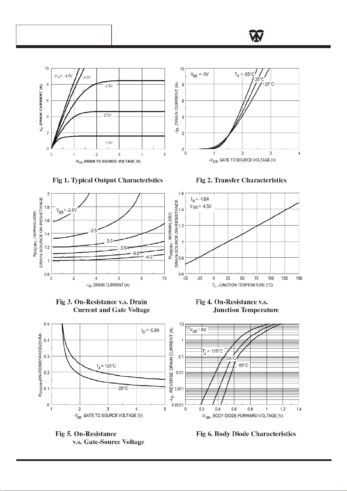
Characteristics Curve
WEITRON
WEITRON
http://www.weitron.com.tw
3/5 07-Nov-08
Page 4
4/5
WTK9431
WEITRON
WEITRON
http://www.weitron.com.tw
07-Nov-08
Page 5
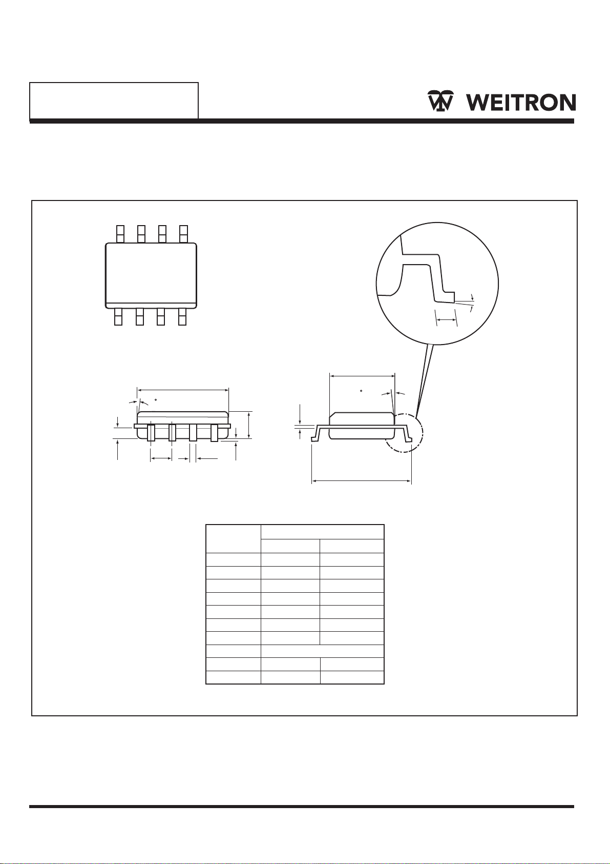
WTK9431
SOP-8 Package Outline Dimensions
1
D
(4X)
7
A
A2
e
B
1A
C
Unit:mm
θ
L
E1
7(4X)
eB
WEITRON
http://www.weitron.com.tw
SYMBOLS
A
A1
B
C
D
E1
Be
e
L
θ
MILLIMETERS
MIN
1.35
0.10
0.35
0.18
4.69
3.56
5.70
MAX
1.75
0.20
0.45
0.23
4.98
4.06
6.30
1.27 BSC
0.60
0.80
0˚
5/5
8˚
07-Nov-08
 Loading...