

Datasheet WT8043N24, WT8043N20P8, WT8043N20P7, WT8043N20P4, WT8043N20P1 Datasheet (WELTREND)
...Page 1

WT8043
Synchronous Signal discriminator
for Multi-Sync Display Monitor
Jan. 30, 1996
Description
The WT8043 is a silicon monolithic circuit designed for synchronous signal
processing of multi-sync display monitors capable of coping with many kinds of PC's
and workstations. It can be applied to display monitors supporting standard IBM
VGA, VESA super VGA and IBM 8514/A video modes. It can also be used in other
high-end display monitors supporting non-standard video modes with user-defined
horizontal/vertical frequency ranges.
WT8043 incorporates many functional circuits, horizontal/vertical frequency
discrimination, display mode selection, and synchronous pulse polarity detection, into
a single chip. Therefore, by using WT8043, monitor makers can shrink the PC board
size, reduce the material cost with fewer components, and reduce labor cost as well.
Features
• Accepting separate H&V Synchronous signals with any polarities
• Support VESA VGA (640x480, 640x400, 640x350), VESA SVGA (800x600),
European SVGA (800x600), VESA new SVGA (800x600), XGA (1024x768)
and 1280x1024.
• Also including NEC (24K) mode, 3 VESA New 75Hz timing modes and Apple
MAC II (35k) mode.
• Capable of processing horizontal frequency from 25KHz to 80KHz
• Capable of processing vertical frequency from 50Hz to 120Hz
• Standard IBM video mode control outputs (1024x768, 640x480, 640x400,
640x350)
• Six non-standard horizontal frequency control outputs with predefined frequency
range. (users can define their own horizontal frequency range)
• Fixed polarity horizontal and vertical synchronous signals output
• Power supply voltage: 5V, but mode select control output and frequency
discrimination control output, these open collector outputs can be combined with
pull high resistor, pull up to 12V.
Application
• Auto size control for Multi-Sync Display Monitors
Weltrend Semiconductor, Inc.
2F., No. 24, Industry E. 9th Rd.
Science-Based Industrial Park
Hsin-Chu, Taiwan, R.O.C.
Tel: 886-35-780241
Fax: 886-35-770419
1
Page 2
WT8043
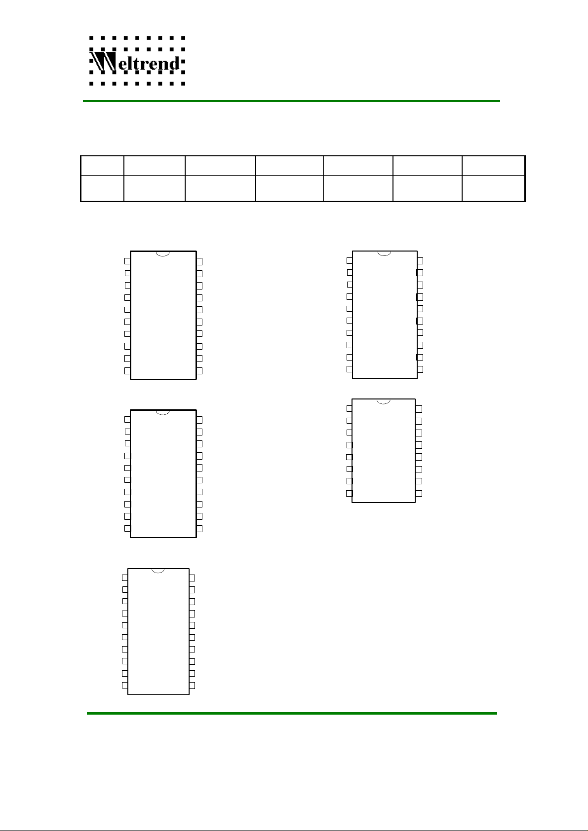
Ordering Information
Part No.
WT8043N16 WT8043N20P1 WT8043N20P4 WT8043N20P7 WT8043N20P8 WT8043N24
Package P-DIP 16L P-DIP 20L P-DIP 20L P-DIP 20L P-DIP 20L
Pin Configuration
HSin
VSin
F45K
F36K
Vss
F33K
HSin
VSin
F36K
Vss
WT8043N20P8
1
2
3
4
5
6
7
8
9
10
20
19
18
17
16
15
14
13
12
11
WT8043N16
1
2
3
4
5
6
7
8 9
16
15
14
13
12
11
10
VDD
1024x768(60K,75)
1024x768(57K)
1024x768(I)
800x600(48K)
800x600(46.8K,75)
800x600(37.5K)
640x480
640x400
640x350
VDD
1024x768 (I)
800x600(37.5K)
800x600(35K)
640x480
640x400
640x350
F33K
OSCin
OSCout
HSin
VSin
H_out
V_out
F52K
F45K
F36K
Vss
OSCin
OSCout
HSin
VSin
H_out
V_out
F45K
F36K
Vss
F33K
WT8043N20P1
1
2
3
4
5
6
7
8
9
10 11
20
19
18
17
16
15
14
13
12
WT8043N20P4
1
2
3
4
5
6
7
8
9
10
20
19
18
17
16
14
12
11
15
13
VDD
1024x768(57K)
1024x768 (NI)
1024x768 (I)
800x600(48K)
800x600(37.5K)
800x600(35K)
640x480
640x400
640x350
VDD
1024x768(57K)
1024x768 (NI)
1024x768 (I)
800x600(48K)
800x600(37.5K)
800x600(35K)
640x480
640x400
640x350
OSCin
OSCout
H_out
V_out
OSCin
OSCout
H_out
V_out
P-DIP 24L
(skinny type)
OSCin
OSCout
HSin
VSin
H_out
V_out
F52K
F45K
F36K
Vss
WT8043N20P7
1
2
3
4
5
6
7
8
9
10
20
19
18
17
16
15
14
13
12
11
VDD
1024x768(57K)
1024x768 (NI)
1024x768 (I)
800x600(48K)
800x600(37.5K)
800x600(35K)
640x480
640x400
NEC
Weltrend Semiconductor, Inc.
2F., No. 24, Industry E. 9th Rd.
Science-Based Industrial Park
Hsin-Chu, Taiwan, R.O.C.
Tel: 886-35-780241
Fax: 886-35-770419
2
Page 3
WT8043
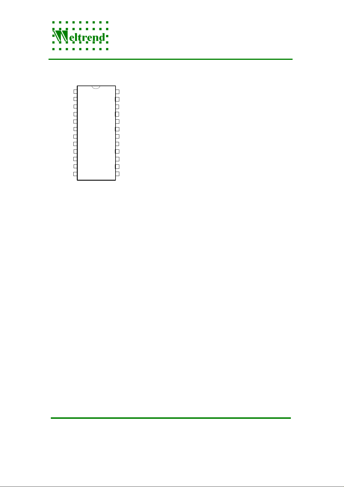
WT8043N24
OSCin
OSCout
HSin
VSin
H_out
1280x1024
(64k)
V_out
F60K
F52K
F45K
F36K
Vss F33K
1
2
3
4
5
6
7
8
9
10
11
12
24
23
22
21
20
19
18
17
16
15
14
13
VDD
F72K
1024x768(57K)
1024x768 (NI)
1024x768 (I)
800x600(48K)
800x600(37.5K)
800x600(35K)
640x480
640x400
640x350
Weltrend Semiconductor, Inc.
2F., No. 24, Industry E. 9th Rd.
Science-Based Industrial Park
Hsin-Chu, Taiwan, R.O.C.
Tel: 886-35-780241
Fax: 886-35-770419
2
Page 4
WT8043
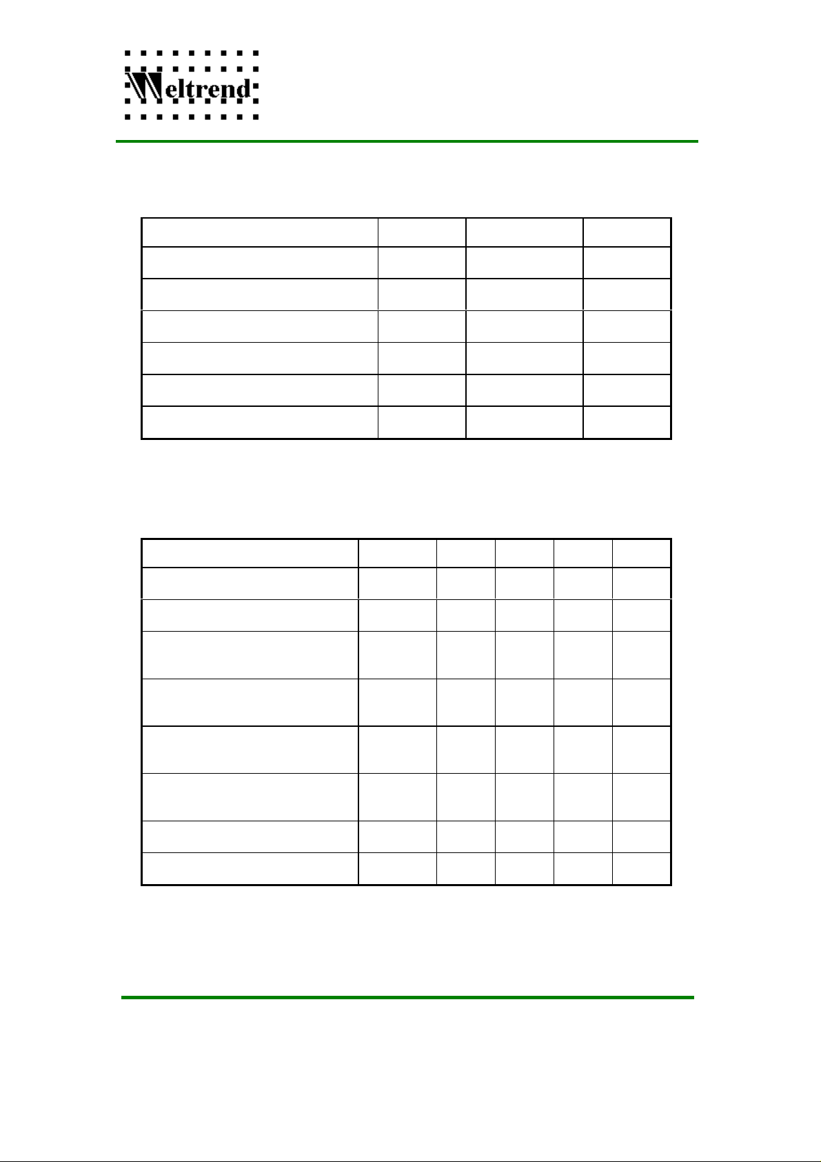
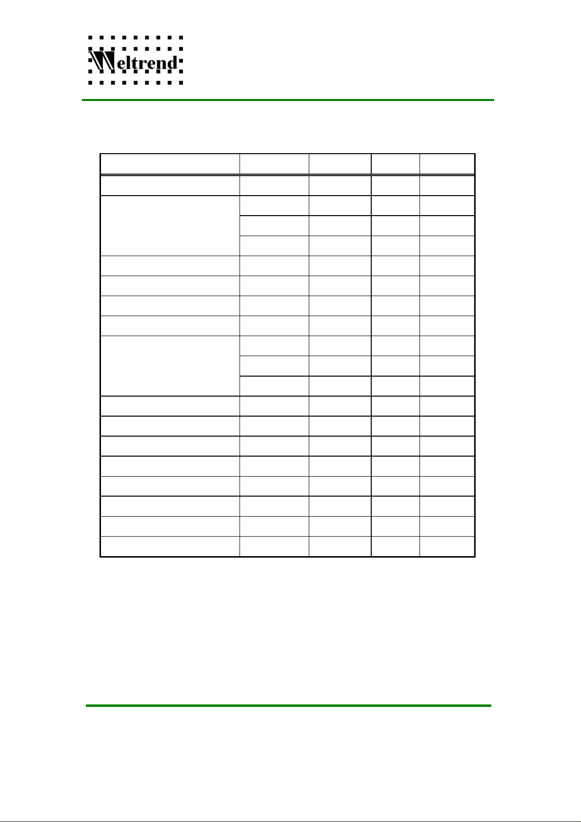
Absolute Maximum Ratings
Item Symbol Value Unit
Digital Supply Voltage V
Horizontal Sync. Input Voltage
DD
V
Vertical Sync. Input Voltage V
Power Dissipation P
Operating Temperature Range
Storage Temperature Range T
T
OPT
STG
Recommended Operating Conditions
Item Symbol Min. Typ. Max. Unit
Digital Supply Voltage V
Supply Current (Oscillator on) I
Synchronous Input Voltage
Low
(5) 4.5 5 5.5 V
DD
P
V
IL
HS
VS
D
5.5 V
VDD(5)+0.3
V
VDD(5)+0.3 V
300 mW
0~70
-40~125
°C
°C
0.8 V
mA
Synchronous Input Voltage
High
Horizontal Synchronous
Frequency Range
Vertical Synchronous
Frequency Range
Crystal Clock Frequency
F
Open Drain Pull High Voltage V
Weltrend Semiconductor, Inc.
2F., No. 24, Industry E. 9th Rd.
Science-Based Industrial Park
Hsin-Chu, Taiwan, R.O.C.
Tel: 886-35-780241
Fax: 886-35-770419
V
IH
F
H
F
V
CLK
OH
2.4 4 5.0 V
25 - 80 KHz
50 - 120 Hz
3.5764 3.58 3.5836 MHz
8 12 V
3
Page 5
WT8043
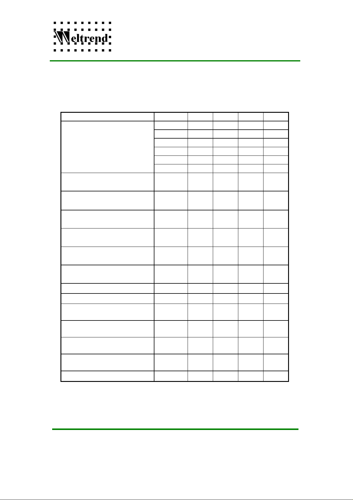
Electrical Characteristics
(VDD=5V, T
=25°C, Crystal=3.58MHz)
OPT
Item Symbol Min. Typ. Max. Unit
F33K 32.95 - 33.05 KHz
F36.2K 36.15 - 36.25 KHz
Discrimintaion of H. F45K 44.95 - 45.05 KHz
Synchronous Frequency F52K 51.95 - 52.05 KHz
F62K 61.95 - 62.05 KHz
F72K 71.95 - 72.05 KHz
Output Low (H-out, V-out)
When I
OL
= 4mA
Output High (H-out, V-out)
When I
= -400µA
OH
Open Collector Output Low
When I
OL
= 6mA
Output Sink Current (H-out,
V-out) When V
OL1
= 0.4V
Output Drive Current (H-out,
V-out) When V
OH1
= 2.4V
Open Drain Sink Current
When V
OL2
= 0.4V
Input H_SYNC Pulse Width W
Input V_SYNC Pulse Width W
H_SYNC, Output Pulse delay,
V
OL1
V
OH1
V
OL2
I
OL1
¡ýI
OH1
I
OL2
H_SYNC
V_SYNC
T
DHS
0.4 V
2.4 V
0.4 V
4 mA
¡ý 400
6 mA
0.56 4
0.56 833
60 nS
respect to Hsin
V_SYNC, Output Pulse delay,
T
VHS
60 nS
respect to Vsin
Upper Trigger Input Point
V
UTP
2.0 V
(H_IN, V_IN)
Lower Trigger Input Point
V
LTP
0.8 V
(H_IN, V_IN)
Noise Margin (H_IN, V_IN)
V
NM
1.75 V
µA
µS
µS
Weltrend Semiconductor, Inc.
2F., No. 24, Industry E. 9th Rd.
Science-Based Industrial Park
Hsin-Chu, Taiwan, R.O.C.
Tel: 886-35-780241
Fax: 886-35-770419
4
Page 6
WT8043
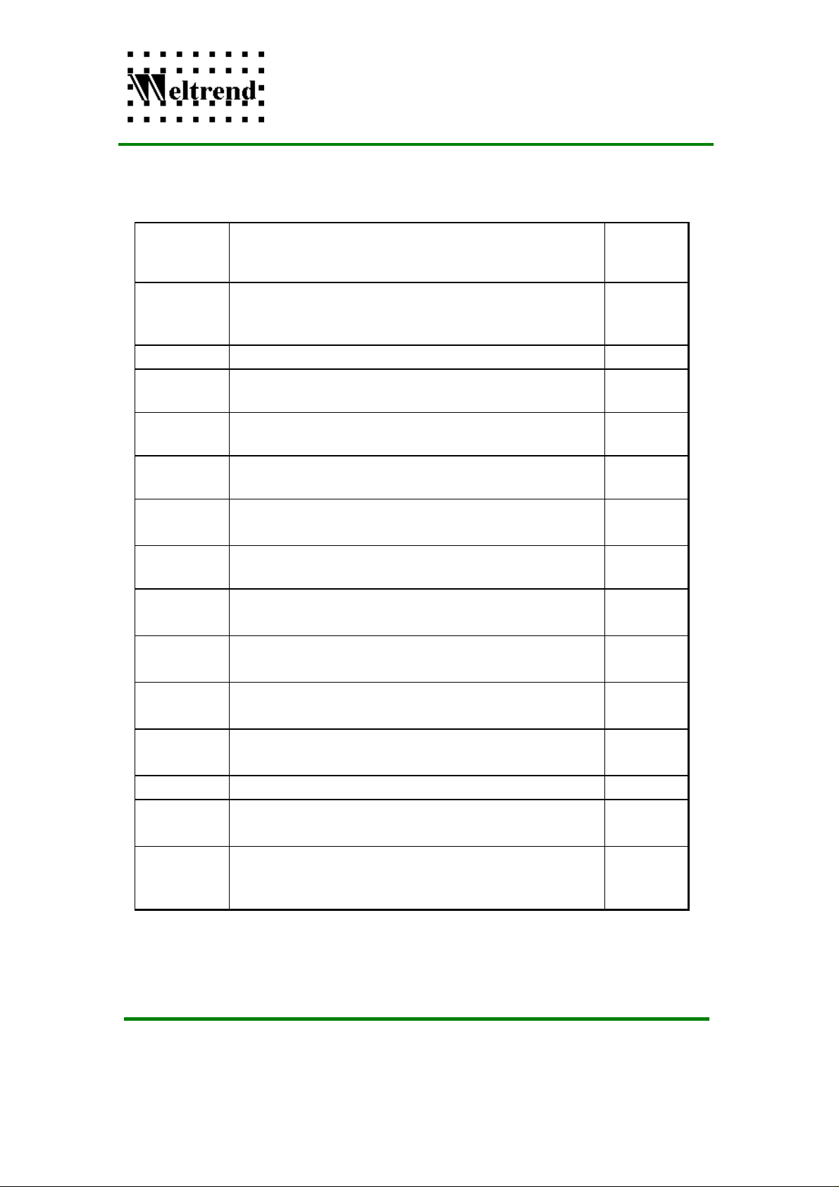
Application Information
Structure
Name Function of
Terminal
OSCin A clock generating circuit is built into the chip. So if
a resonator is connected to OSCin / OSCout, a clock
signal can be obtained
OSCout
HSin Input terminal of horizontal synchronous Signal I, TTL
VSin Input terminal of vertical synchronous Signal I, TTL
H_out Output pin, active low, fixed polarity of original
1280 x 1024 1280x1024 mode control output O,
V_OUT
Referent to OSCin pin
H_sync signal w/ same pulse width
Output pin, active low, fixed polarity of original
V_sync signal w/ same pulse width
Compatible
Compatible
O, TTL
Compatible
open drain
O, TTL
Compatible
I
F60K H, frequency input 60k discrimination > 60k then
active low, < 60k then high
O,
open drain
F52K > 52k then active low, < 52k then high O,
open drain
F45K > 45k then active low, < 45k then high O,
open drain
F36K > 36k then active low, < 36k then high O,
open drain
Vss Ground
F33K > 33k then active low, < 33k then high O,
open drain
640 x 350 Mode seclect control output, if IBM VGA 640x350
mode, or VESA VGA 640x350 mode, then active
O,
open drain
low, else high state output
Weltrend Semiconductor, Inc.
2F., No. 24, Industry E. 9th Rd.
Science-Based Industrial Park
Hsin-Chu, Taiwan, R.O.C.
Tel: 886-35-780241
Fax: 886-35-770419
5
Page 7
WT8043
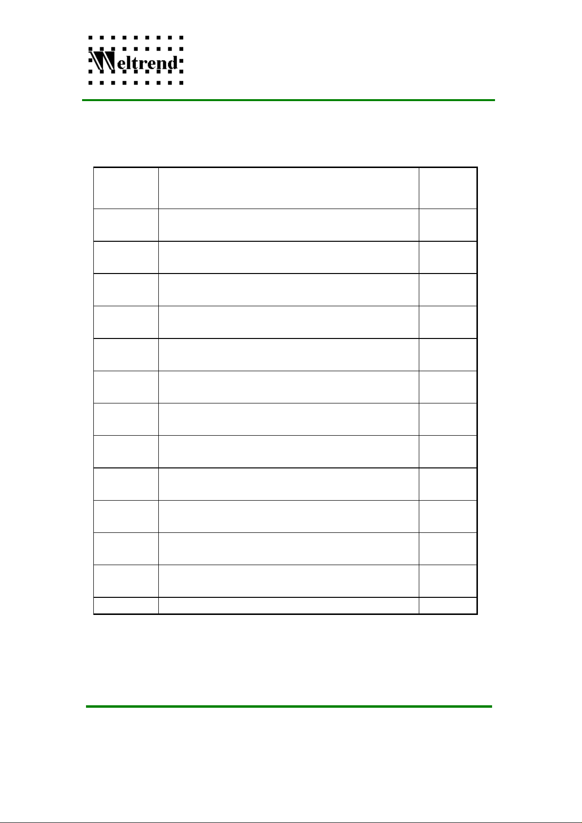
(Contd.)
Structure
Name Function of
Terminal
NEC NEC 640 x 400, 24.8kHz/ 56.4Hz timing mode O,
open drain
640 x 400 If IBM VGA 640 x 400 mode, or VESA VGA 640 x
400 mode then active "low"
640 x 480 If IBM VGA 640 x 480 mode, or VESA VGA 640 x
480 mode then active "low"
O,
open drain
O,
open drain
800 x 600 VESA super VGA mode Hsync freq. 35kHz O,
open drain
800 x 600 European super VGA mode Hsync freq. 37.5kHz O,
open drain
800 x 600
(46.8k,75)
VESA new 75Hz Timing mode O,
open drain
800 x 600 VESA new super VGA mode Hsync freq. 48kHz O,
open drain
1024x768 (I)
IBM 8514/A interlace mode O,
open drain
1024x768
(NI)
1024x768
(57k)
1024x768
(60k, 75)
F72K Hysnc freq. discrimination control output if > 72 kHz
IBM 8514/A non-interlace mode O,
open drain
XGA 1024x768 mode Hsync freq. 57kHz O,
open drain
VESA new 75Hz Timing mode O,
open drain
O,
then active low, else high
open drain
VDD 5 Volts power supply
Weltrend Semiconductor, Inc.
2F., No. 24, Industry E. 9th Rd.
Science-Based Industrial Park
Hsin-Chu, Taiwan, R.O.C.
Tel: 886-35-780241
Fax: 886-35-770419
6
Page 8
WT8043
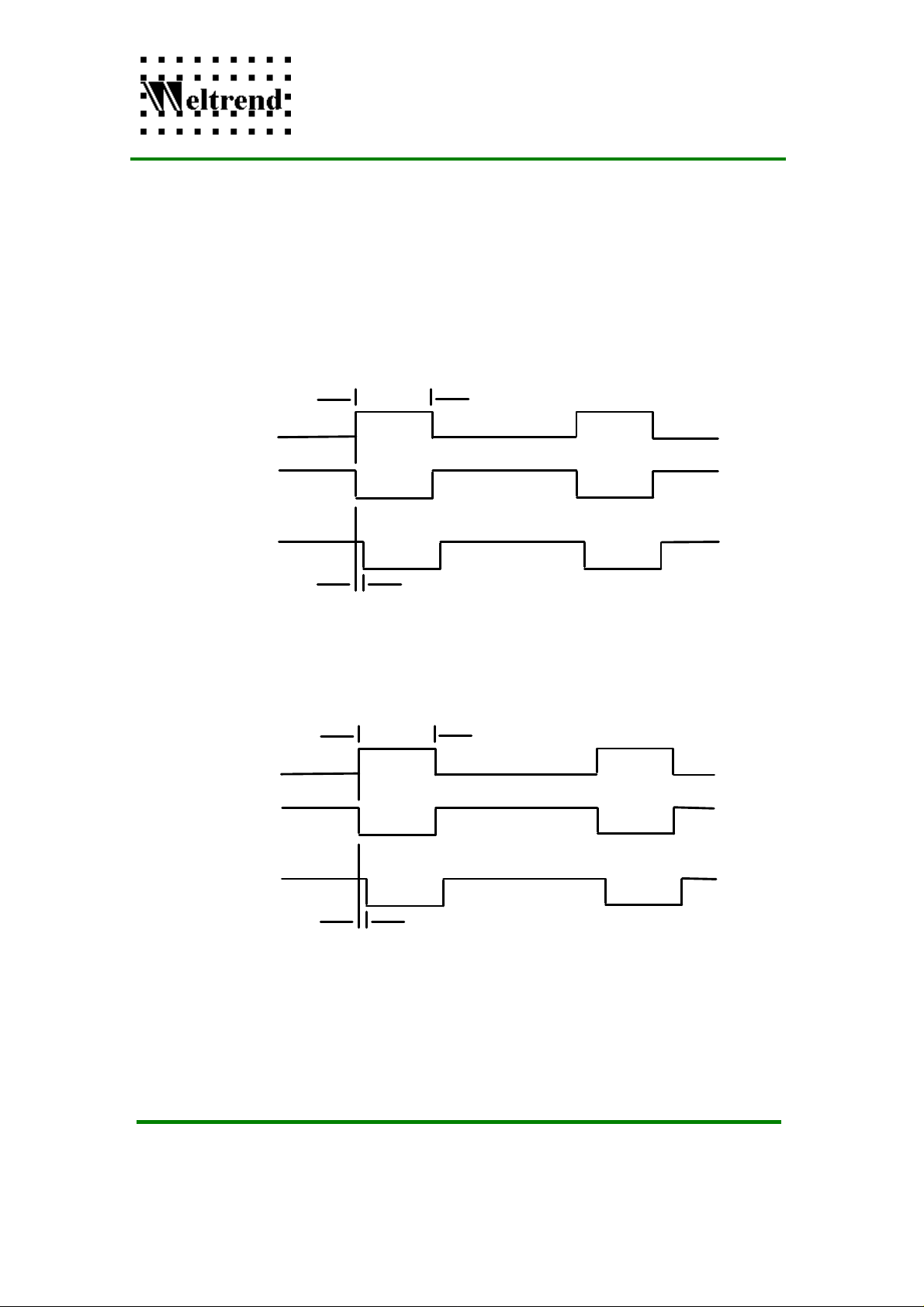
Time Chart
• Hin - Hout
W
H-SYNC
IN_H
IN_H
H_OUT
T
• Vin - Vout
IN_V
IN_V
V_OUT
+
-
dhs
+
W
V-SYNC
-
T
dvs
Weltrend Semiconductor, Inc.
2F., No. 24, Industry E. 9th Rd.
Science-Based Industrial Park
Hsin-Chu, Taiwan, R.O.C.
Tel: 886-35-780241
Fax: 886-35-770419
7
Page 9
WT8043
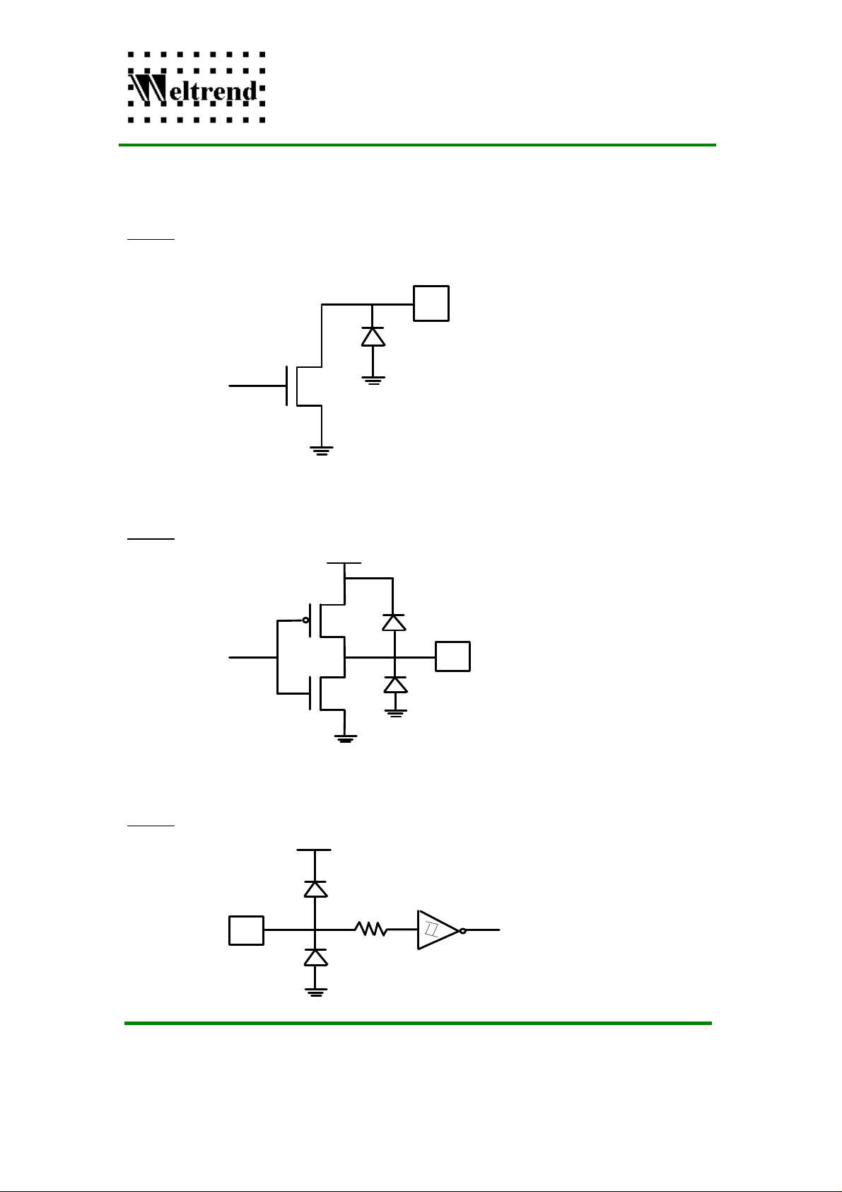
Structure of Terminal
Type 1
Type 2
PAD
Open Drain NMOS can
pull up by external resistor,
no connector must be pull
down or floating.
VDD
Type 3
PAD
VDD
PAD
Weltrend Semiconductor, Inc.
2F., No. 24, Industry E. 9th Rd.
Science-Based Industrial Park
Hsin-Chu, Taiwan, R.O.C.
Tel: 886-35-780241
Fax: 886-35-770419
8
Page 10

WT8043
Weltrend Semiconductor, Inc.
2F., No. 24, Industry E. 9th Rd.
Science-Based Industrial Park
Hsin-Chu, Taiwan, R.O.C.
Tel: 886-35-780241
Fax: 886-35-770419
9
Page 11

WT8043
Block Diagram I
Figure 1-1 WT8043N20P1 Functional Block Diagram
Weltrend Semiconductor, Inc.
2F., No. 24, Industry E. 9th Rd.
Science-Based Industrial Park
Hsin-Chu, Taiwan, R.O.C.
Tel: 886-35-780241
Fax: 886-35-770419
10
Page 12

WT8043
Block Diagram II
Figure 1-2 WT8043N24 Functional Block Diagram
Weltrend Semiconductor, Inc.
2F., No. 24, Industry E. 9th Rd.
Science-Based Industrial Park
Hsin-Chu, Taiwan, R.O.C.
Tel: 886-35-780241
Fax: 886-35-770419
11
Page 13

WT8043
Appication Description
General Description
Figure 1-1 and 1-2 is a simplified functional block diagram of the WT8043. It
includes the following functional blocks: sync pulse polarity detector; horizontal
and vertical frequency discriminator, mode selector.
The Sync pulse polarity detector accepts separete H and V sync signals with any
polarities. It determines their polarities and sends the polarity information to the
mode selector for video mode selection. It alos generates -H and -V signals in spite
of their input polarities.
The H and V frequency discriminator determines the frequency range of H and V
sync signals. The mode selector determines which operating video mode it should
be, according to the frequency range and polarity of H and V sync signals. The
operating video modes include the standard IBM VGA (640x350, 640x400,
640x480), super VGA (800x600) and IBM8514/A (Inerlaced, Non-interlaced),
VESA VGA & SVGA mode, VESA new SVGA mode, XGA (1024x768), and
1280x1024 mode, also including NEC 24kHz and 3 VESA New 75Hz timing
modes.
The mode selector also generates output signals that represent the frequency range
of H. sync signal. The H sync signal is divided into 6 frequency ranges (3 ranges
for WT8043N20) according to Fig. 2, WT8043 has preset the discriminating points
between frequency ranges. However, it also offers the flexibility for providing
user-defined discriminating points for non-standard video modes.
The digital noise filter is used for rejecting noise on the incoming horizontal and
vertical synchronous signals. The input section uses two techniques to improve
noise rejec-tion. So the low level noise and the large short duration noise spikes
will be rejected. Horizontal synchronous pulse width under 0.56 µs and vertical
synchronous pulse width under 0.56 µs will be considered as noise.
Weltrend Semiconductor, Inc.
2F., No. 24, Industry E. 9th Rd.
Science-Based Industrial Park
Hsin-Chu, Taiwan, R.O.C.
Tel: 886-35-780241
Fax: 886-35-770419
12
Page 14

WT8043
H/V Frequency Divisions and Video Modes
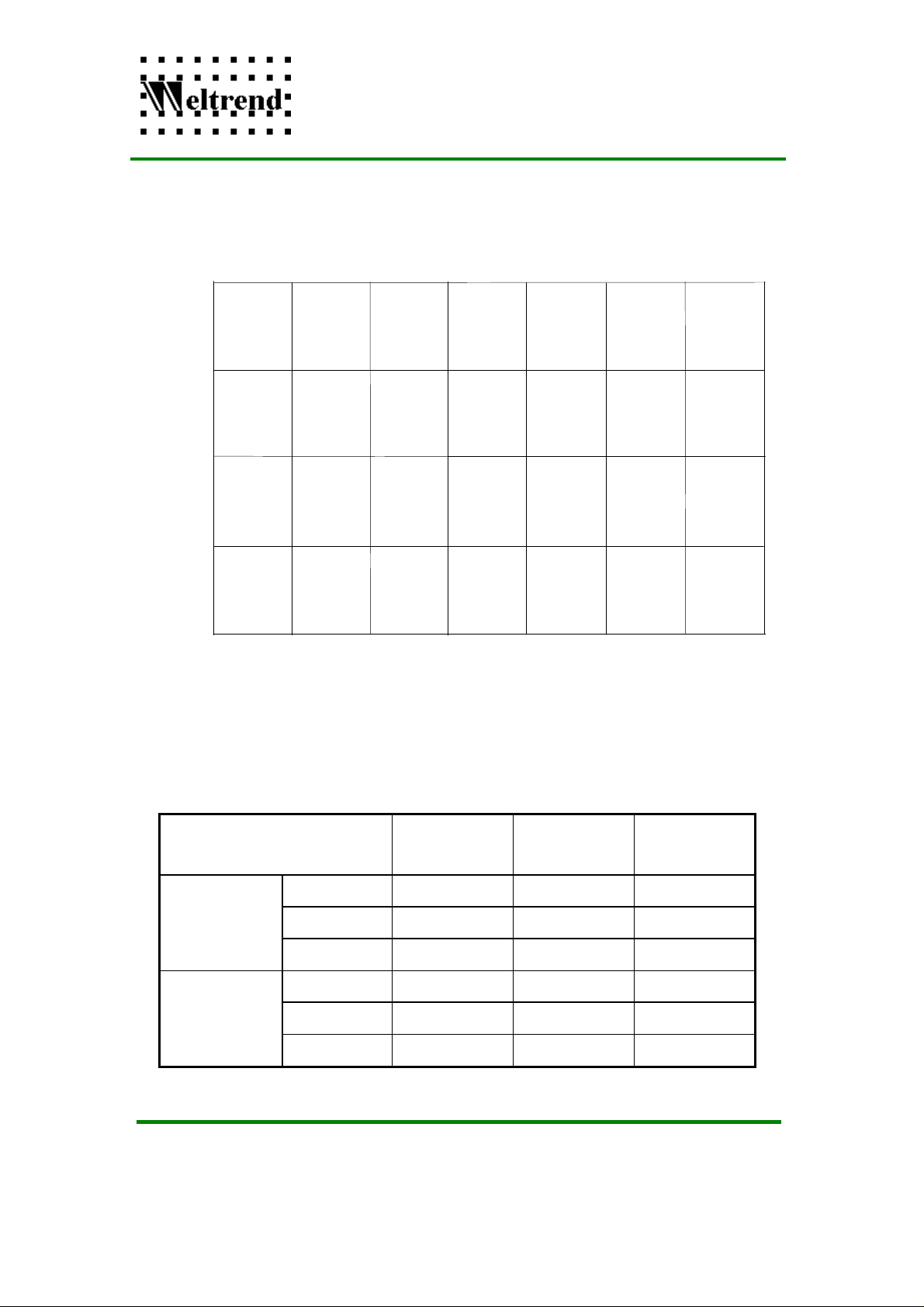
Figure 2 illustrates the typical frequency ranges of H and V sync signals for
display monitors. The operating video modes are determined by the H and V
frequencies, and occasionally, by their polarities. The typical video modes of
display monitors include the NEC 24k mode, IBM VGA, VESA VGA, European
VGA/Super VGA, Apple MAC II, VESA Super VGA, IBM 8514/A,3 VESA New
75Hz modes, XGA, and 1280x 1024.
WT8043 can determine 18 standard video modes (as shown in Table 1) according
to H and V frequencies and polari-ties. These standard video modes include the
IBM VGA, VESA VGA, VESA super VGA and IBM 8514/A. This provides the
users with the capability to adjust the screen size for different modes.
WT8043 pre-sets the discriminating points both on H and V frequencies. The
discriminating points for H sync are 33KHz, 36.2KHz, 45KHz, 52KHz, 62KHz
and 72KHz. These discriminating points will be able to identify various video
modes as shown in Fig. 2. WT8043 also provides the flexibility for users to define
these discriminating points through mask option.
The tolerance for H sync frequency discrimination is 0.05KHz. For instance, the
33KHz discriminating point will be able to distinguish the H sync frequency that is
either "less than or euqal to" 32.95KHz, or "greater than or equal to" 33.05KHz.
There is an ambiguous region between 32.95KHz and 33.05KHz.
WT8043 has three discriminating points, 64Hz, 73.5Hz and 78Hz, for the V sync
signal as shown in Fig.2. The tolerance is 0.01Hz. The discrimination results of V
sync frequency are used internally for mode selection.
Base on the package consideration, IBM VGA mode and VESA VGA mode (both
have same resolution: 640x480, 640x400, 640x350) are decoded on same open
Drain structure output pins (e.g. pin 14 to pin 16 for N20P1 pin type package). In
case of these whole 6 modes decoding is needed, the horizontal frequency
discrimination pin F33k or F36k must take into consideration. The horizontal
frequency of IBM VGA mode is 31.4kHz, and VESA IBM VGA mode is 37.5kHz.
Using F33k or F36k pin can clearly identify these two standard modes. The
decoding circuit is attached on application section for reference.
Weltrend Semiconductor, Inc.
2F., No. 24, Industry E. 9th Rd.
Science-Based Industrial Park
Hsin-Chu, Taiwan, R.O.C.
Tel: 886-35-780241
Fax: 886-35-770419
13
Page 15
WT8043
Table 1: Graphaic Standard and Frequencies
¡I
Graphic Standard Resolution Horizontal Vertical Polarities
NEC Timing 640 x 400 24.8KHz 56.4Hz -,-
640 x 350 31.5KHz 70Hz +,-
IBM VGA 640 x 400 31.5KHz 70Hz -,+
640 x 480 31.5KHz 60Hz -,-
Mac II 640 x 480 35.0KHz 67Hz
New 72Hz 640 x 480 38.6KHz 72Hz -,+
VESA Super VGA 800 x 600 35.2KHz 56Hz
IBM 8514/A interlaced 1024 x 768 35.5KHz 86Hz
640 x 350 37.5KHz 83Hz +,-
VESA VGA 640 x 400 37.5KHz 83Hz -,+
640 x 480 37.5KHz 72Hz -,-
VESA New 75Hz Timing 640 x 480 37.5KHz 75Hz -,-
European Super VGA 800 x 600 37.5KHz 60Hz
VESA New 75Hz Timing 800 x 600 46.8KHz 75Hz
VESA New Super VGA 800 x 600 48.0KHz 72Hz
IBM 8514/A Non-interlaced 1024 x 768 48.5KHz 60Hz
VESA New 1024 x 768 1024 x 768 56.5KHz 72Hz
VESA New 75Hz Timing 1024 x 768 60.0KHz 75Hz
Work Station 1280 x1024 1280 x 1024 64.0KHz 60Hz
Weltrend Semiconductor, Inc.
2F., No. 24, Industry E. 9th Rd.
Science-Based Industrial Park
Hsin-Chu, Taiwan, R.O.C.
Tel: 886-35-780241
Fax: 886-35-770419
14
Page 16
WT8043
Figure 2: H/V Frequency Division and Video Mode
Fv (Hz)
78
73.5
64
30
11
640X400
(24k, 56)
640X350
(32k, 70)
(+,-)
640X400
(32k, 70)
(-,+)
640X480
(32k, 60)
(-,-)
28 33
1024X768
(35k, 87)
640X480
(35k, 67)
MAC II
800X600
(35k, 56)
640X350
(37k, 84)
640X400
(37k, 84)
640X480
(38.6k, 72)
36.2
(+,-)
(-,+)
(37k, 75)
(-,-)
640X480
(37k, 73)
(-,-)
640X480
(-,+)
800X600
(38k, 60)
45
832X624
(50k, 70)
800X600
(47k, 75)
800X600
(48k, 72)
1024X768
(48k, 60)
1024X768
(60k, 75)
1024X768
(56.5k, 72)
52 62
1280X1024
(64k, 60)
Fh(KHz)
Table 2: IBM VGA/ VESA VGA Decoding Table
PIN
Mode
640 x 480 640 x 400 640 x 350
640 x 480 0 1 1
IBM VGA 640 x 400 1 0 1
640 x 350 1 1 0
640 x 480 0 1 1
VESA VGA 640 x 400 1 0 1
640 x 350 1 1 0
Weltrend Semiconductor, Inc.
2F., No. 24, Industry E. 9th Rd.
Science-Based Industrial Park
Hsin-Chu, Taiwan, R.O.C.
Tel: 886-35-780241
Fax: 886-35-770419
15
Page 17
WT8043
Horizontal Frequency Discriminator
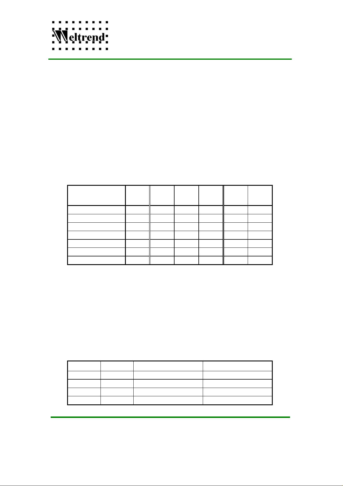
There are 3 horizontal frequency discriminator pins on 20 pin type package:
36.2kHz, 45kHz, 52kHz (for N20P1), 33kHz, 36.2kHz, 45kHz (for N20P4); 2
frequency discriminator pins on 16 pin type package: 33kHz, 36.2kHz and 6
frequency discriminator pins on 24 pin type package: 33kHz, 36.2kHz, 45kHz,
52kHz, 62kHz and 72kHz. Please refer to table 3 for the logical truth table of
these pins. These frequency discriminator pins can pull up to +12V through a
resistor, sink current to the open drain structure must keep under 6mA (ref. P4
Electrical Characteristics). These frequency discriminator pins output can be used
for CS Capacitor Control directly as well as other application.
Table 3: Truth table of Frequency discriminator
Signal
Hsync
F33K F36.2K F45K F52K F62K F72K
Hs < 33k 1 1 1 1 1 1
36.2k > Hs > 33k 0 1 1 1 1 1
45k > Hs > 36.2k 0 0 1 1 1 1
52k > Hs > 45k 0 0 0 1 1 1
62k > Hs > 52k 0 0 0 0 1 1
72k > Hs > 62k 0 0 0 0 0 1
Hs > 72k 0 0 0 0 0 0
SYNC Output State Description
Both H_out / V_out duplicate Hsin/Vsin in the same frequency and pulse width,
but are fixed at negative polarity. And H_out/ V_out have their own cut-off
frequency: 15kHz for H_Sync and 30Hz for V_Sync. While the frequency of input
signal is less than the cut-off frequency, the output will keep in low state. Please
refer to the Table 4.
Table 4:
Hsin Vsin H_out V_out
>15kHz >30Hz Negative polarity Hsin Negative polarity Vsin
>15kHz <30Hz Negative polarity Hsin Low state
<15kHz >30Hz Low state Negative polarity Vsin
<15kHz <30Hz Low state Low state
Weltrend Semiconductor, Inc.
2F., No. 24, Industry E. 9th Rd.
Science-Based Industrial Park
Hsin-Chu, Taiwan, R.O.C.
Tel: 886-35-780241
Fax: 886-35-770419
16
Page 18

WT8043
Application Circuit I
Weltrend Semiconductor, Inc.
2F., No. 24, Industry E. 9th Rd.
Science-Based Industrial Park
Hsin-Chu, Taiwan, R.O.C.
Tel: 886-35-780241
Fax: 886-35-770419
17
Page 19

WT8043
Application Cirucit II
Weltrend Semiconductor, Inc.
2F., No. 24, Industry E. 9th Rd.
Science-Based Industrial Park
Hsin-Chu, Taiwan, R.O.C.
Tel: 886-35-780241
Fax: 886-35-770419
18
Page 20
WT8043
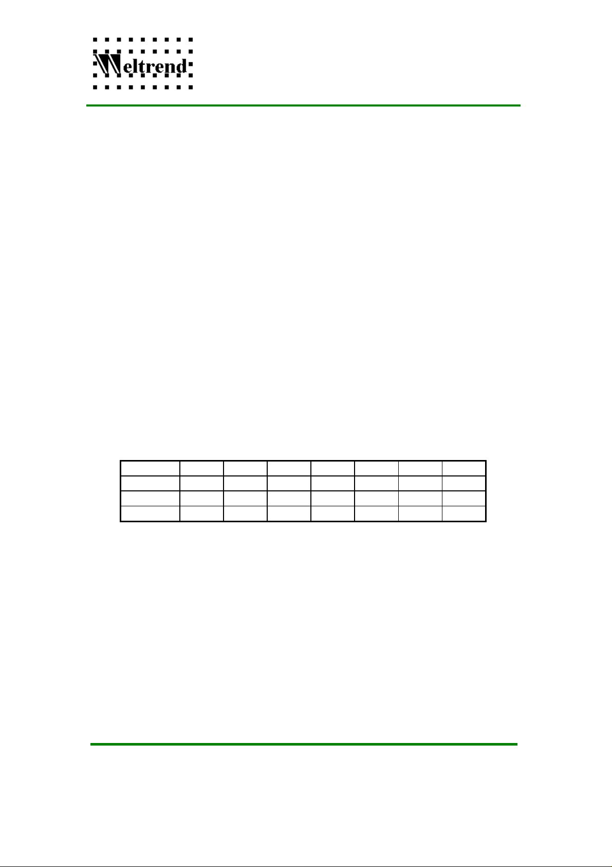
Physical Dimension
A B C D E F G
16L 754 250 130 100 130 355 300
20L 1024 250 130 100 130 355 300
24L skinny 1250 260 130 100 130 355 300
* Dimension in mil
* 1mm = 39.37 mil
Weltrend Semiconductor, Inc.
2F., No. 24, Industry E. 9th Rd.
Science-Based Industrial Park
Hsin-Chu, Taiwan, R.O.C.
Tel: 886-35-780241
Fax: 886-35-770419
19
 Loading...