

Page 1
WT6018
Digital Monitor Controller
Ver. 1.41 Jul-31-1998
GENERAL DESCRIPTION
The WT6018 is a member of WT60XX microcontroller family. It is specially designed for digital
controlled multi-sync monitor. It contains 8-bit CPU, 8K bytes ROM, 288 bytes RAM, 14 PWMs,
parallel I/O, SYNC processor, timer, DDC interface (slave mode I2C interface with DDC1), two 4-bit
A/D convertors and watch-dog timer.
FEATURES
* 8-bit 6502 compatible CPU, 4MHz operating frequency
* 8192 bytes ROM, 288 bytes SRAM
* 8MHz crystal oscillator
* 14 channels 8-bit/62.5kHz PWM outputs (8 open drain outputs & 6 CMOS outputs)
* Sync signal processor with H+V separation, frequency calculation, H/V polarity detection/control
* Three free-running sync signal outputs for burn-in test (64kHz/62.5Hz, 48kHz/75Hz, 31kHz/60Hz)
* Self-test pattern generator generates cross hatch picture
* Provide half frequency input and output
* DDC interface supports VESA DDC1/DDC2B standard
* Watch-dog timer (0.524 second)
* Maximum 25 programmable I/O pins
* One 8-bit programmable timer
* Two 4-bit A/D converter
* One external interrupt request
* Built-in low VDD voltage reset
* +5V power supply
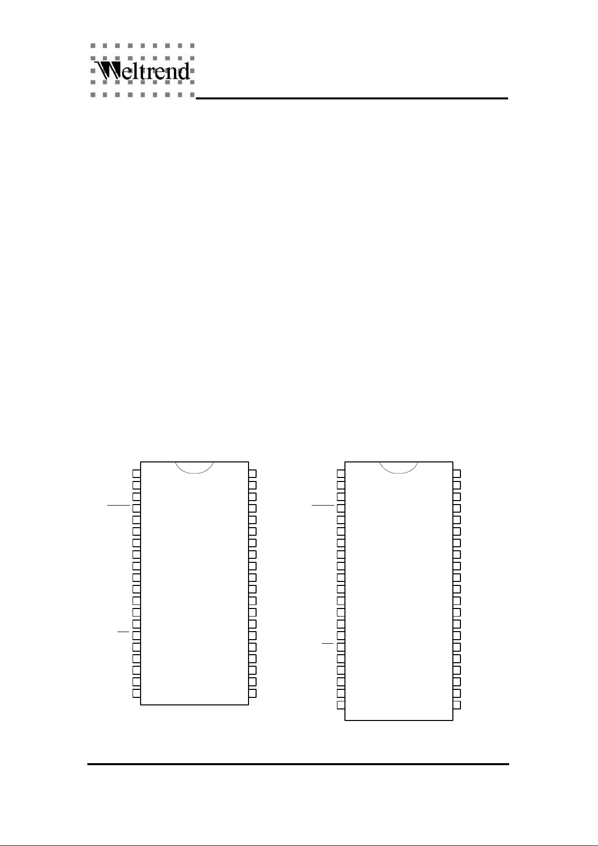
PIN ASSIGNMENT
1
DA2
2
DA1
3
DA0
RESET
OSCO
OSCI
PB3/PAT
PB1/HLFI
PB0/HLFO
PB6/IRQ
4
5
VDD
6
GND
7
8
9
PB5
10
PB4
11
12
PB2
13
14
15
16
PC7 SCL/PD0
17
PC6
18
PC5
19
PC4
40
39
38
37
36
35
34
33
32
31
30
29
28
27
26
25
24
23
22
2120
VSYNC
HSYNC
DA3
DA4
DA5
DA6
DA7
PA7/HSO
PA6/VSO
PA5/DA13
PA4/DA12
PA3/DA11
PA2/DA10
PA1/DA9
PA0/DA8
SDA/PD1
PC0/AD0
PC1/AD1
PC2PC3
42-Pin SDIP40-Pin PDIP
1
DA2
2
DA1
3
DA0
RESET
OSCO
OSCI
PB3/PAT
PB1/HLFI
PB0/HLFO
PB6/IRQ
4
5
VDD
6
7
GND
8
9
10
PB5
11
PB4
12
13
PB2
14
15
16
17
PC7 SCL/PD0
18
PC6
19
PC5
20
PC4
42
41
40
39
38
37
36
35
34
33
32
31
30
29
28
27
26
25
24
23
2221
VSYNC
HSYNC
DA3
DA4
DA5
DA6
DA7
PA7/HSO
PA6/VSO
PA5/DA13
PA4/DA12
PA3/DA11
PA2/DA10
PA1/DA9
PA0/DA8
SDA/PD1
PC0/AD0
PC1/AD1
PC2PC3
* I2C is a trademark of Philips Corporation.
* DDC is a trademark of Video Electronics Standard Association (VESA).
Weltrend Semiconductor, Inc.
1
Page 2
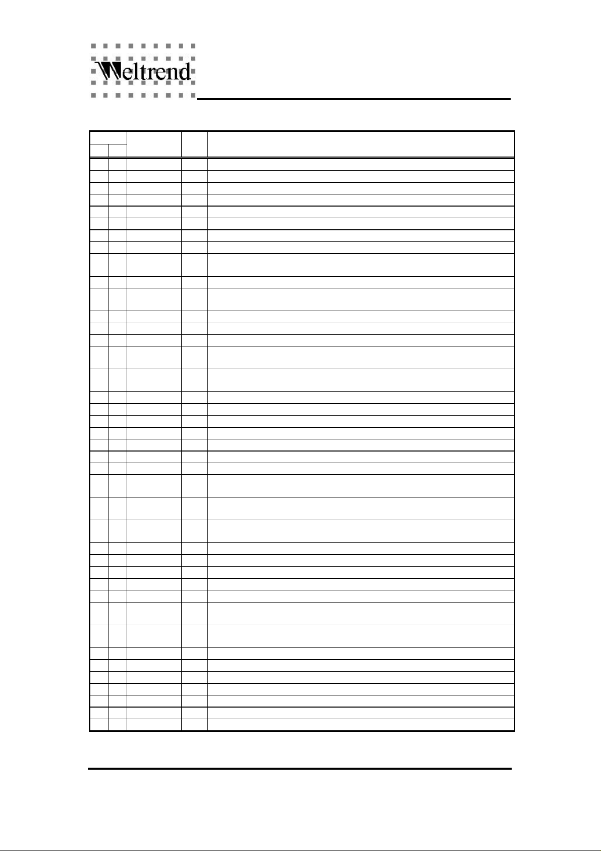
PIN DESCRIPTION
Pin No.
40 42
1 1 DA2 O
2 2 DA1 O
3 3 DA0 O
4 4 /RESET I
5 5 VDD
6 7 GND
7 8 OSCO O
8 9 OSCI I
9 10 PB5 I/O
10 11 PB4 I/O
11 12 PB3/PAT I/O
12 13 PB2 I/O
13 14 PB1/HLFI I/O
14 15 PB0/HLFO I/O
15 16 PB6/IRQ I/O
16 17 PC7 I/O
17 18 PC6 I/O
18 19 PC5 I/O
19 20 PC4 I/O
20 21 PC3 I/O
21 22 PC2 I/O
22 23 PC1/AD1 I/O
23 24 PC0/AD0 I/O
24 25 SDA/PD1 I/O
25 26 SCL/PD0 I/O
26 27 PA0/DA8 I/O
27 28 PA1/DA9 I/O
28 29 PA2/DA10 I/O
29 30 PA3/DA11 I/O
30 31 PA4/DA12 I/O
31 32 PA5/DA13 I/O
32 33 PA6/VSO I/O
33 34 PA7/HSO I/O
34 35 DA7 O
35 36 DA6 O
36 38 DA5 O
37 39 DA4 O
38 40 DA3 O
39 41 HSYNC I
40 42 VSYNC I
Pin Name I/O Descriptions
WT6018
Digital Monitor Controller
Ver. 1.41 Jul-31-1998
D/A converter 2. Open-drain output. External applied voltage can up to 10V.
D/A converter 1. Open-drain output. External applied voltage can up to 10V.
D/A converter 0. Open-drain output. External applied voltage can up to 10V.
Reset. Active low. Schmitt trigger input, Internal pull high.
Power supply (+5V).
Ground (0V).
Oscillator Output. Connects a 8MHz crystal.
Oscillator Input. Connects a 8MHz crystal.
I/O Port B5. When it is an input pin, it has an internal pull-up resistor. When it is
an output pin, the sink current is 5mA and the source current is 5mA.
I/O Port B4. Same as PB5.
I/O Port B3 or self-test pattern output. When as an I/O port, it is same as PB5.
When it is configured to test pattern output, a vedio signal is output.
I/O Port B2. Same as PB5.
I/O Port B1 or half frequency input.
I/O Port B0 or half frequency output.
I/O Port B6 or Interrupt Request . When as interrupt request input, it has an
internal pull high resistor. When as an I/O port, it is same as PB5.
I/O Port C7. When it is an input pin, it has an internal pull-up resistor. When it is
an output pin, the sink current is 10mA and the source current is 5mA.
I/O Port C6. Same as PC7.
I/O Port C5. Same as PC7.
I/O Port C4. Same as PC7.
I/O Port C3. Same as PC7.
I/O Port C2. Same as PC7.
I/O Port C1 or A/D converter input 0.
I/O Port C0 or A/D converter input 1.
DDC serial data or I/O Port D1. When it is a DDC interface pin, It is an open-
drain output. When as an I/O port, it is same as Port B.
DDC serial clock or I/O Port D0. When it is a DDC interface pin, It is an opendrain output. When as an I/O port, it is same as Port B.
I/O Port A0 or D/A converter 8. This pin can be the output of D/A converter 8
(source/sink = 5mA) or an I/O pin (source = -100uA, sink = 5mA).
I/O Port A1 or D/A converter 9. Same as PA0/DA8.
I/O Port A2 or D/A converter 10. Same as PA0/DA8.
I/O Port A3 or D/A converter 11. Same as PA0/DA8.
I/O Port A4 or D/A converter 12. Same as PA0/DA8.
I/O Port A5 or D/A converter 13. Same as PA0/DA8.
I/O Port A6 / VSYNC OUT. This pin can be the output of VSYNC or an I/O pin.
When as an I/O pin, it is same as PA0.
I/O Port A7 / HSYNC OUT. This pin can be the output of HSYNC or an I/O pin.
When as an I/O pin, it is same as PA0.
D/A converter 7. Open-drain output. External applied voltage can up to 10V.
D/A converter 6. Open-drain output. External applied voltage can up to 10V.
D/A converter 5. Open-drain output. External applied voltage can up to 10V.
D/A converter 4. Open-drain output. External applied voltage can up to 10V.
D/A converter 3. Open-drain output. External applied voltage can up to 10V.
HSYNC input. Schmitt trigger input.
VSYNC input. Schmitt trigger input.
Weltrend Semiconductor, Inc.
2
Page 3
WT6018
Digital Monitor Controller
Ver. 1.41 Jul-31-1998
FUNCTIONAL DESCRIPTION
CPU
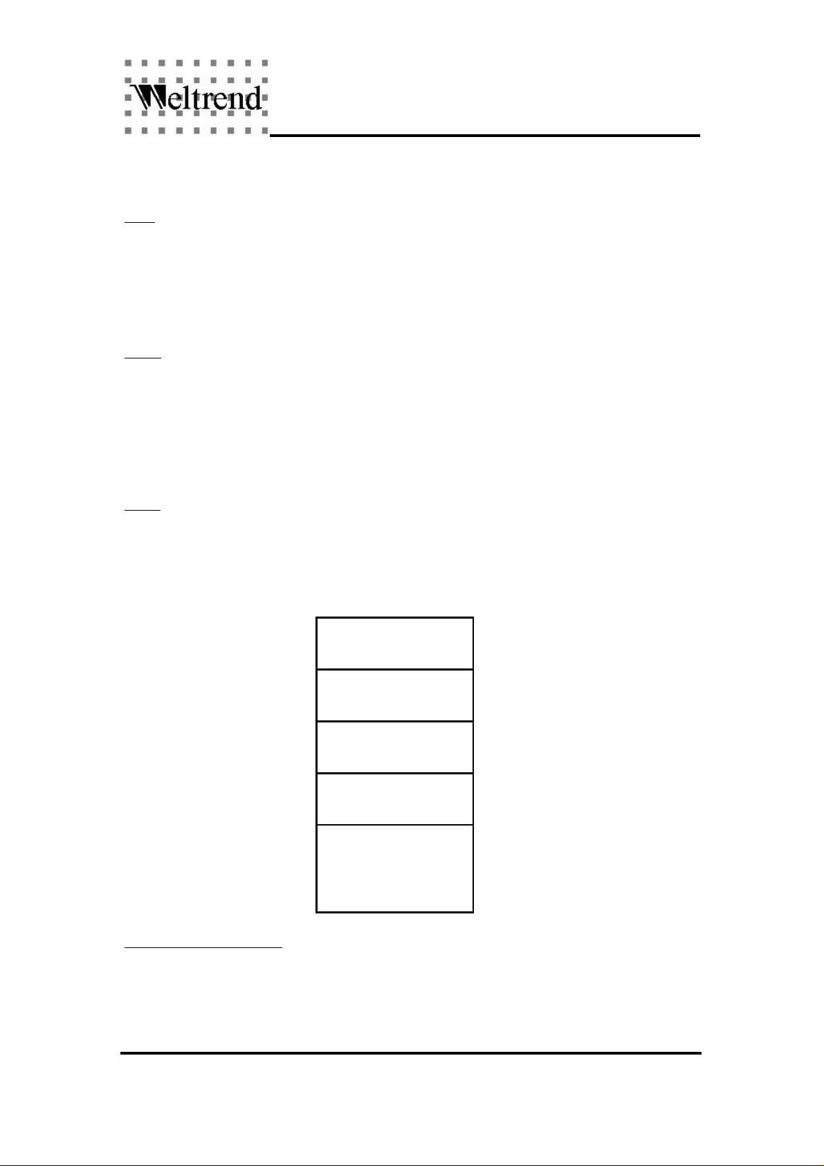
The CPU core is 6502 compatible, operating frequency is 4MHz. Address bus is 16-bit and data bus is
8-bit. the non-maskable interrupt (/NMI) of 6502 is changed to maskable interrupt and is defined as
the INT0. The interrupt request (/IRQ) of 6502 is defined as the INT1.
Default stack pointer is 01FFH.
Please refer the 6502 reference menu for more detail.
ROM
8192 bytes maskable ROM is provided for program codes.
Address is located from E000H to FFFFH.
The following addresses are reserved for special purpose :
FFFAH (low byte) and FFFBH (high byte) : INT0 interrupt vector.
FFFCH (low byte) and FFFDH (high byte) : program reset vector.
FFFEH (low byte) and FFFFH (high byte) : INT1 interrupt vector.
RAM
Built-in 288 bytes SRAM, address is located from 0080H to 019FH. Because the initial stack pointer
is 01FFH, so program must set proper stack pointer when program starts. A recommended value is
019FH.
0000H
:
0020H
0021H
:
007FH
0080H
:
019FH
01A0H
:
DFFFH
E000H
:
:
:
FFFFH
REGISTERS
Reserved
RAM
Reserved
ROM
Low VDD Voltage Reset
A VDD voltage detector is built inside the chip. When VDD is below 4.0 volts, the whole chip will be
reset just like power-on-reset.
Note that the 4.0 volts varies with temperature and process. Please refer the electrical characteristics.
Weltrend Semiconductor, Inc.
3
Page 4
WT6018
Digital Monitor Controller
Ver. 1.41 Jul-31-1998
PWM D/A Converter
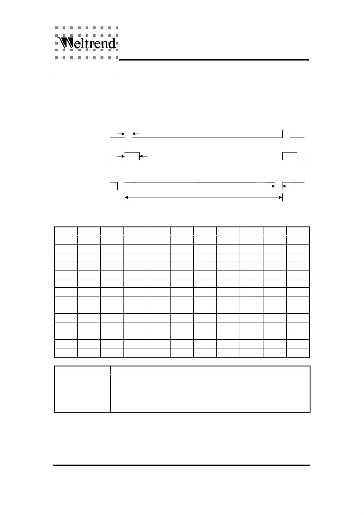
The WT6018 provides 14 PWM D/A converters. DA0 to DA7 are open-drain outputs and external
applied voltage on these pins can be up to 10 volts. DA8 to DA13 are 5 volts push-pull CMOS outputs
and are shared with I/O Port PA0 to PA5. All D/A converters are 62.5kHz frequency with 8-bit
resolution. Each D/A converter is controlled by the corresponding register (REG#00H to REG#0DH),
the duty cycle can be programmed from 1/256 (data = 01H) to 255/256 (data = FFH).
Duty cycle = 1/256
62.5ns
Duty cycle = 2/256
125ns
62.5ns
Duty cycle = 255/256
1/62.5kHz=16us
To program the PWM D/A converters, write the corresponding registers ( REG#00H to REG#0DH).
Address R/W Initial Bit7 Bit6 Bit5 Bit4 Bit3 Bit2 Bit1 Bit0
0000H R/W 80H DA07DA06DA05DA04DA03DA02DA01DA0
0001H R/W 80H DA17DA16DA15DA14DA13DA12DA11DA1
0002H R/W 80H DA27DA26DA25DA24DA23DA22DA21DA2
0003H R/W 80H DA37DA36DA35DA34DA33DA32DA31DA3
0004H R/W 80H DA47DA46DA45DA44DA43DA42DA41DA4
0005H R/W 80H DA57DA56DA55DA54DA53DA52DA51DA5
0006H R/W 80H DA67DA66DA65DA64DA63DA62DA61DA6
0007H R/W 80H DA77DA76DA75DA74DA73DA72DA71DA7
0008H R/W 80H DA87DA86DA85DA84DA83DA82DA81DA8
0009H R/W 80H DA97DA96DA95DA94DA93DA92DA91DA9
000AH R/W 80H DA107DA106DA105DA104DA103DA102DA101DA10
000BH R/W 80H DA117DA116DA115DA114DA113DA112DA111DA11
000CH R/W 80H DA127DA126DA125DA124DA123DA122DA121DA12
000DH R/W 80H DA137DA136DA135DA134DA133DA132DA131DA13
Bit Name Bit value
DAx7-DAx0 01H : 1/256 duty cycle
02H : 2/256 duty cycle
03H : 3/256 duty cycle
:
FFH : 255/256 duty cycle
0
0
0
0
0
0
0
0
0
0
0
0
0
0
** Do not write 00H to the PWM registers. This will cause unstable
output on the corresponding pin.
Weltrend Semiconductor, Inc.
4
Page 5
WT6018
Digital Monitor Controller
Ver. 1.41 Jul-31-1998
I/O Ports
Port_A :
Pin PA0/DA8 - general purpose I/O shared with DA8 output.
Pin PA1/DA9 - general purpose I/O shared with DA9 output.
Pin PA2/DA10 - general purpose I/O shared with DA10 output.
Pin PA3/DA11 - general purpose I/O shared with DA11 output.
Pin PA4/DA12 - general purpose I/O shared with DA12 output.
Pin PA5/DA13 - general purpose I/O shared with DA13 output.
Pin PA6/VSO - general purpose I/O shared with VSYNC output.
Pin PA7/HSO - general purpose I/O shared with HSYNC output.
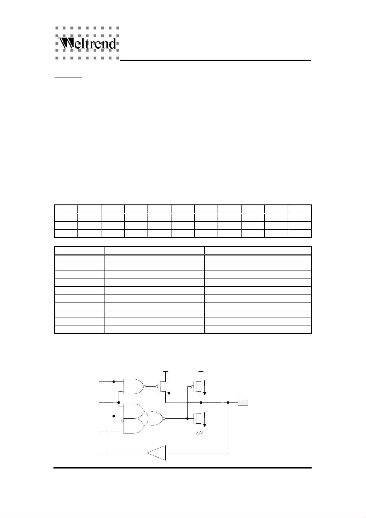
Port_A is controlled by REG#10H & REG#11H. In REG#10H, each corresponding bit enables
HSYNC output, VSYNC output or D/A converter output when it is "1". If the corresponding bit is "0",
the output level is decided by REG#11H. In REG#11H, if the I/O corresponding bit (PAn) is "0", the
output is low level (IOL=5mA). If PAn bit is "1", the output is high level (IOH= -100uA) and can be
used as an input.
Address R/W Initial Bit7 Bit6 Bit5 Bit4 Bit3 Bit2 Bit1 Bit0
0010H W 00H EHO EVO EDA13 EDA12 EDA11 EDA10 EDA9 EDA8
0011H W FFH PA7W PA6W PA5W PA4W PA3W PA2W PA1W PA0W
0011H R -- PA7R PA6R PA5R PA4R PA3R PA2R PA1R PA0R
Bit Name Bit value = “1” Bit value = “0”
EHO Enable PA7 as HSYNC output. PA7 as general purpose I/O.
EVO Enable PA6 as VSYNC output. PA6 as general purpose I/O.
EDA13 Enable PA5 as DA13 output. PA5 as general purpose I/O.
EDA12 Enable PA4 as DA12 output. PA4 as general purpose I/O.
EDA11 Enable PA3 as DA11 output. PA3 as general purpose I/O.
EDA10 Enable PA2 as DA10 output. PA2 as general purpose I/O.
EDA9 Enable PA1 as DA9 output. PA1 as general purpose I/O.
EDA8 Enable PA0 as DA8 output. PA0 as general purpose I/O.
PA7W - PA0W Outputs high level (IOH= -100uA). Outputs low level (IOL= 5mA).
PA7R- PA0R Pin is high level. Pin is low level.
* If the program wants to force VSYNC output (VSO pin) in low state, write "0" to PA6 bit first, then
write "0" to EVO bit. This is used to prevent high frequency output on VSO pin when the VSYNC
frequency is increased to read EDID data in DDC1 mode.
EDAx
DAx
PAnW
5mA
100uA
Pin PAn
5mA
PAnR
Weltrend Semiconductor, Inc.
5
Page 6
WT6018
Digital Monitor Controller
Ver. 1.41 Jul-31-1998
Port_B :
Pin PB0/HLFO - general purpose I/O pins shared with half frequency output.
Pin PB1/HLFI - general purpose I/O pins shared with half frequency input.
Pin PB2 - general purpose I/O pins.
Pin PB3/PAT - general purpose I/O pin shared with self-test pattern output.
Pin PB4 to PB5 - general purpose I/O pins.
Pin PB6/IRQB - general purpose I/O pin shared with interrupt request input.
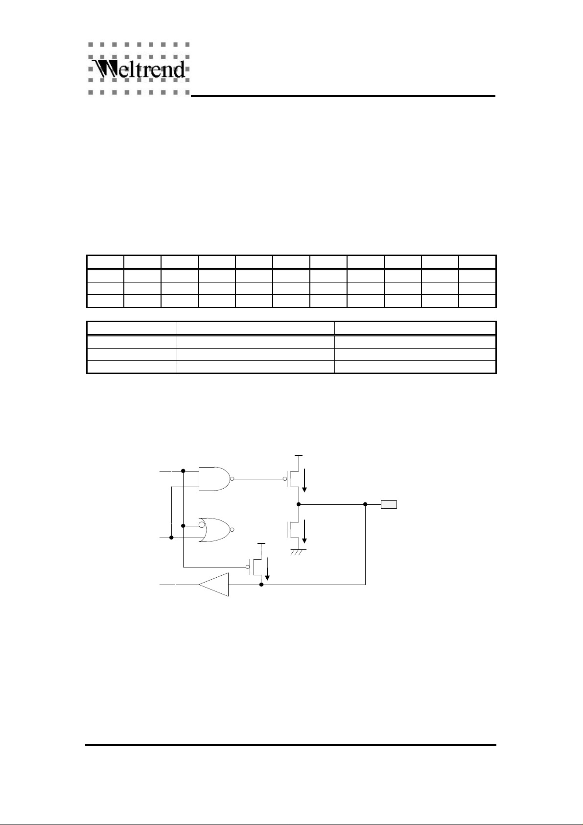
The source/sink current of port_B is 5mA when as an output. When it is input, an internal pull
high resistor is connected.
Address R/W Initial Bit7 Bit6 Bit5 Bit4 Bit3 Bit2 Bit1 Bit0
0012H W 00H 0 PB6OE PB5OE PB4OE PB3OE PB2OE PB1OE PB0OE
0013H W FFH 1 PB6W PB5W PB4W PB3W PB2W PB1W PB0W
0013H R -- -- PB6R PB5R PB4R PB3R PB2R PB1R PB0R
Bit Name Bit value = “1” Bit value = “0”
PB6OE - PB0OE Output enable. Output disable (internal pull-up).
PB6W - PB0W Outputs high level (IOH= -5mA). Outputs low level (IOL= 5mA).
PB6R- PB0R Pin is high level. Pin is low level.
* If ENHALF bit in REG#17H is “1”, the PB0 and PB1 pins are for half frequency function.
* If ENPAT bit in REG#16H is “1”, the PB3 pin becomes self-test pattern output.
* If IEN_X bit in REG#1AH is “1” and PB6OE bit is "0", the PB6 pin becomes interrupt request
input.
PBnOE
5mA
Pin PB0 to PB6
PBnW
100uA
PBnR
Structure of I/O Port B
5mA
Weltrend Semiconductor, Inc.
6
Page 7
WT6018
Digital Monitor Controller
Ver. 1.41 Jul-31-1998
Port_C :
Pin PC0 - general purpose I/O pin shared with 4-bit A/D converter 0 input.
Pin PC1 - general purpose I/O pin shared with 4-bit A/D converter 1 input
Pin PC2 to PC7 - general purpose I/O pins.
The REG#14H defines the I/O direction and the REG#15H controls the output level.
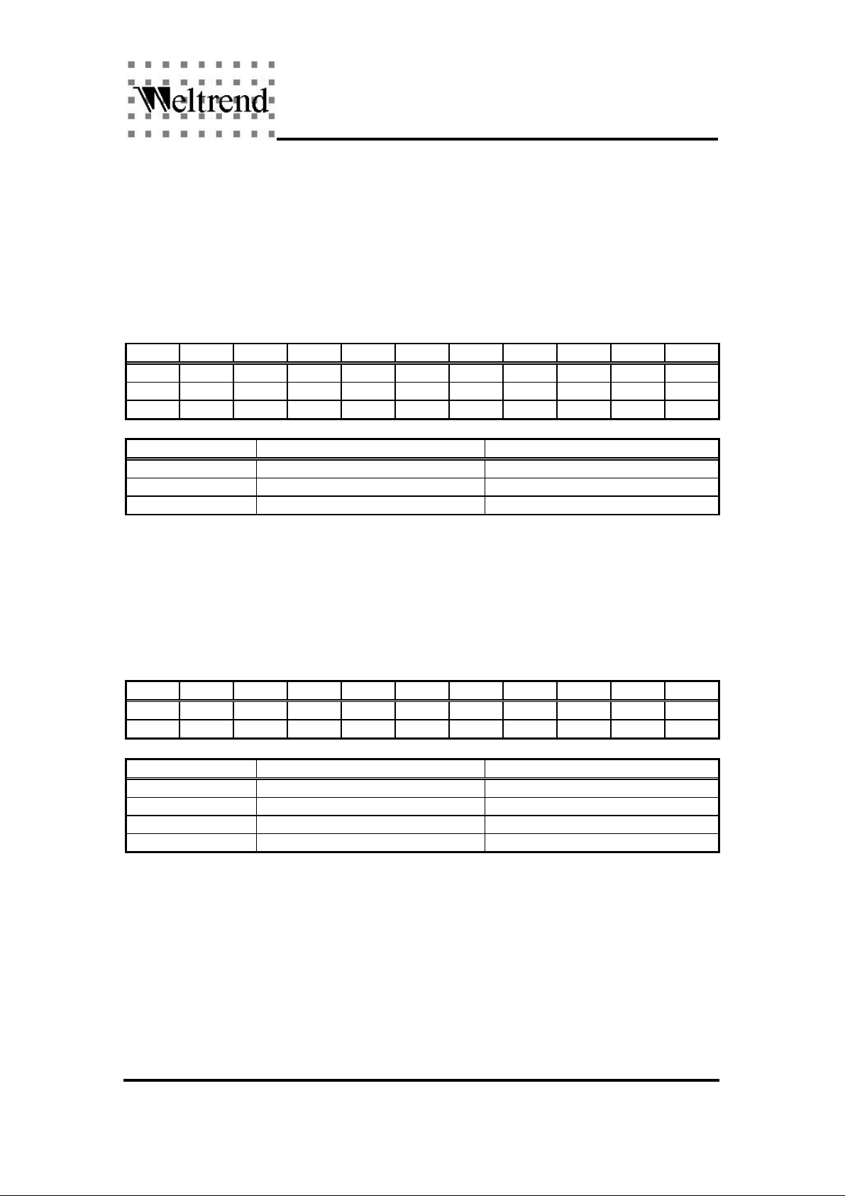
The structure of Port_C is same as the Port_B except the sink current is 10mA. When PC0 and
PC1 are programmed as the A/D converter inputs, the pull high transistor is disconnected.
Address R/W Initial Bit7 Bit6 Bit5 Bit4 Bit3 Bit2 Bit1 Bit0
0014H W 00H PC7OE PC6OE PC5OE PC4OE PC3OE PC2OE PC1OE PC0OE
0015H W FFH PC7W PC6W PC5W PC4W PC3W PC2W PC1W PC0W
0015H R -- PC7R PC6R PC5R PC4R PC3R PC2R PC1R PC0R
Bit Name Bit value = “1” Bit value = “0”
PC7OE - PC0OE Output enable. Output disable (internal pull-up).
PC7W - PC0W Outputs high level (IOH= -5mA). Outputs low level (IOL= 10mA).
PC7R - PC0R Pin is high level. Pin is low level.
Port_D :
Pin SCL/PD0 - general purpose I/O pin shared with DDC interface serial clock.
Pin SDA/PD1 - general purpose I/O pin shared with DDC interface serial data.
The structure of these two pins are same as the PB4 and PB5. Default is DDC interface and can be
changed to I/O port D by setting ENPD bit.
Address R/W Initial Bit7 Bit6 Bit5 Bit4 Bit3 Bit2 Bit1 Bit0
000FH W 00H -- -- -- ENPD PD1OE PD0OE PD1W PD0W
000FH R -- -- -- -- -- -- -- PD1R PD0R
Bit Name Bit value = “1” Bit value = “0”
ENPD Enable I/O Port_D. DDC interface.(open drain)
PD1OE - PD0OE Output enable. Output disable (internal pull-up).
PD1W - PD0W Outputs high level (IOH= -5mA). Outputs low level (IOL= 5mA).
PD1R- PD0R Pin is high level. Pin is low level.
* If program wants to read current status on the I/O pins (any I/O port), do not set output enable bit to
“0”. Because the registers for reading I/O are always indicating the current state on the I/O pins, set
output enable bit to “0” will change the level on the I/O pin. Please reference the I/O pin structure.
Weltrend Semiconductor, Inc.
7
Page 8
WT6018
SELF
Digital Monitor Controller
Ver. 1.41 Jul-31-1998
SYNC Processor
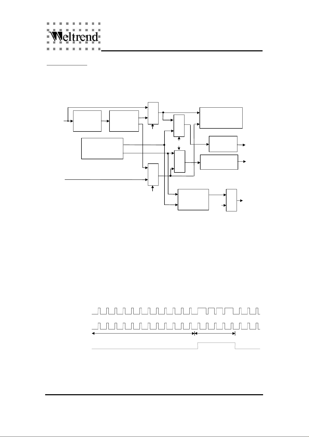
The SYNC processor can : (1) separate the composite sync signal; (2) calculate HSYNC and
VSYNC frequencies; (3) detect polarities of HSYNC and VSYNC inputs; (4) control the output
polarities of HSO and VSO pins. (5) generate free-running horizontal and vertical sync signals for
burn-in test; (6) generate self-test pattern signal.
Mux
H+V
Mux
Mux
Mux
H/V Freq. Counter
H Polarity
Control
V Polarity
detect & control
HSYNC
H Polarity
detect
H/V SYNC
Generator
Sync
Separator
H
V
VSYNC
H+V
Test Pattern
Generator
PB3
Mux
PB3/PAT
Composite Sync Signal Separation
The composite sync signal comes from HSYNC pin and is separated by the sync separator.
The operations of sync separator are:
- detect the polarity and convert composite sync signal to positive polarity.
- extract Vsync
Pulse width less than 8us will be filtered, but the Vsync will be widened about 8us.
- count the pulses during the separated Vsync is low and save the counter value (NH).
- bypass the composite sync pulses before the counter equals to N
H.
- start inserting Hsync pulses after the counter equals to NH until the separated Vsync is low.
- the period of inserted Hsync is decided by the last two bypassed Hsync.
- the pulse width of the inserted Hsync is 2us.
HSO
VSO
Positive H+V
separated Hsync
bypass insert HSYNC
separated Vsync
To decide whether the HSYNC input is a composite sync signal or not, program should check the
frequency of VSYNC first (reset H+V bit to “0”). If the VSYNC frequency is lower than 15.25Hz
(OVF2=1), set H+V bit to “1” and check VSYNC frequency again. If VSYNC still has no frequency,
that is power saving condition, program should reset H+V bit. If it has a valid frequency, the HSYNC
input is composite signal.
Weltrend Semiconductor, Inc.
8
Page 9
WT6018
Digital Monitor Controller
Ver. 1.41 Jul-31-1998
Frequency Calculation
Horizontal frequency and vertical frequencies calculation are done by using one 10-bit up counter.
After power is on, the SYNC processor calculates the vertical frequency first (H/V bit ="0"). A
31.25KHz clock counts the time interval between two VSYNC pulses, then sets the FRDY bit and
generates an INT1 interrupt (if IEN_S bit is "1"). The software can either use interrupt or polling the
FRDY bit to read the correct vertical frequency. After reading the REG#16H, the FRDY bit is cleared
to "0", counter is reset and H/V bit is set. The SYNC processor starts to count horizontal frequency.
The horizontal frequency calculation is done by counting the HSYNC pulses in 8.192 ms. Like the
vertical frequency, the horizontal frequency can be read when the FRDY bit is set or INT1 occurs.
After reading the REG#16H, the FRDY, INT_S and H/V bits are cleared. The SYNC processor starts
to calculate the vertical frequency again, and so on.
The relationships between counter value and frequency are :
Hfreq = (counter value x 122.07) Hz
Vfreq = ( 31250 / counter value ) Hz
The frequency range :
Hfreq range : 122.07 Hz to 124.8 kHz ; Resolution : 122.07Hz
Vfreq range : 30.5 Hz to 31.25 kHz
If counter overflowed, the OVF1 bit will be set to "1". The counter keeps on counting until it
overflowed again. The OVF2 bit and FRDY bit will be set when counter overflowed twice. This is
designed for finding the vertical frequency bellows 15.25Hz. The program should check REG#17H
before reading REG#16H.
Polarity Detect/Control
The polarities of HSYNC and VSYNC are automatically detected and are shown in the H_POL
and V_POL bits. The polarities of HSO and VSO are controlled by the HOP and VOP bits. For
example, set HOP bit to “1”, the HSO pin always outputs positive horizontal sync signal, whatever the
HSYNC input’s polarity is.
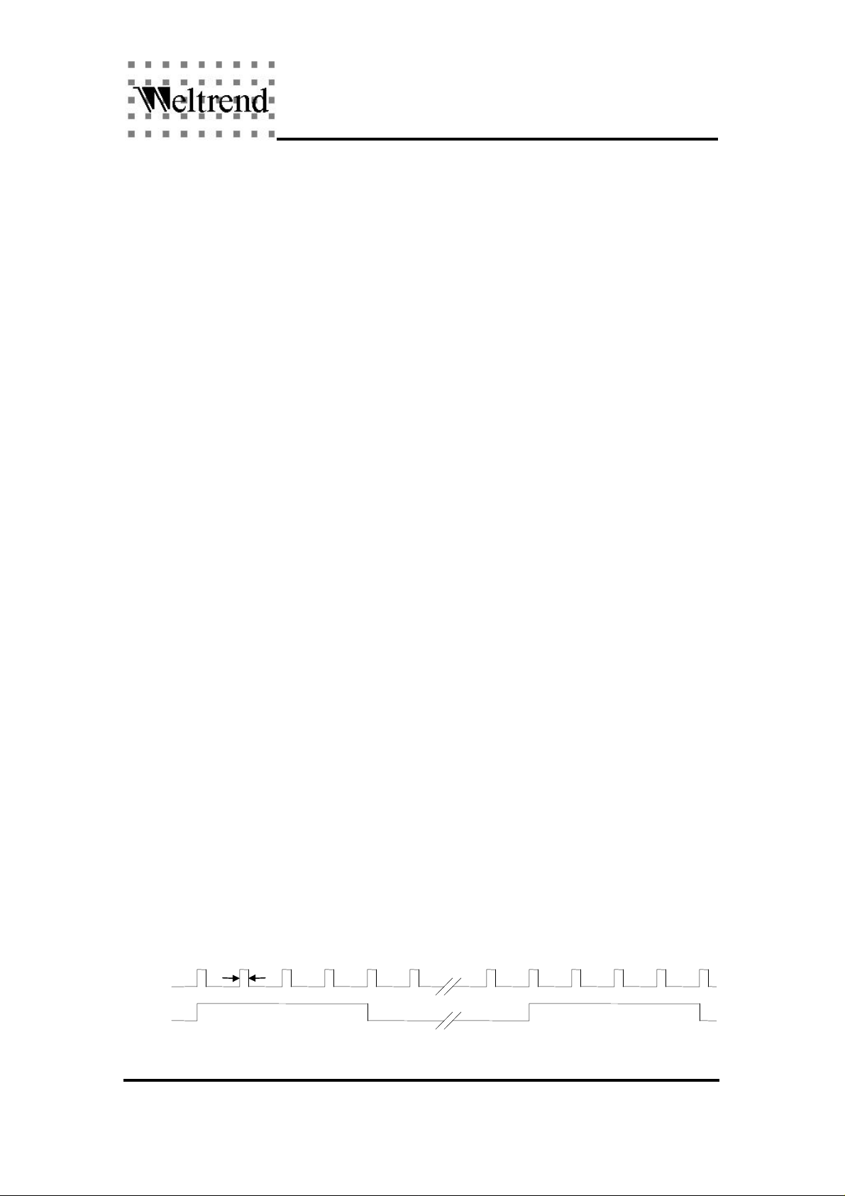
Free-running Sync Signal
The self-generated sync signals are output from HSO and VSO pins if SELF bit is “1”. Three kinds
of frequencies are provided :
(1) Hfreq = 8MHz/125 = 64.0kHz, Vfreq = Hfreq/1024 = 62.5Hz.
(2) Hfreq = 8MHz/167 = 47.9kHz, Vfreq = Hfreq/640 = 74.9Hz.
(3) Hfreq = 8MHz/257 = 31.1kHz, Vfreq = Hfreq/512 = 60.8Hz .
The output polarities are controlled by the HOP and VOP bits.
The pulse width of HSO is 2us and VSO is four HSO cycles. The timing relationship is shown in
the following :
2us
HSO
VSO
Weltrend Semiconductor, Inc.
9
Page 10
WT6018
Digital Monitor Controller
Ver. 1.41 Jul-31-1998
Test Pattern Generation
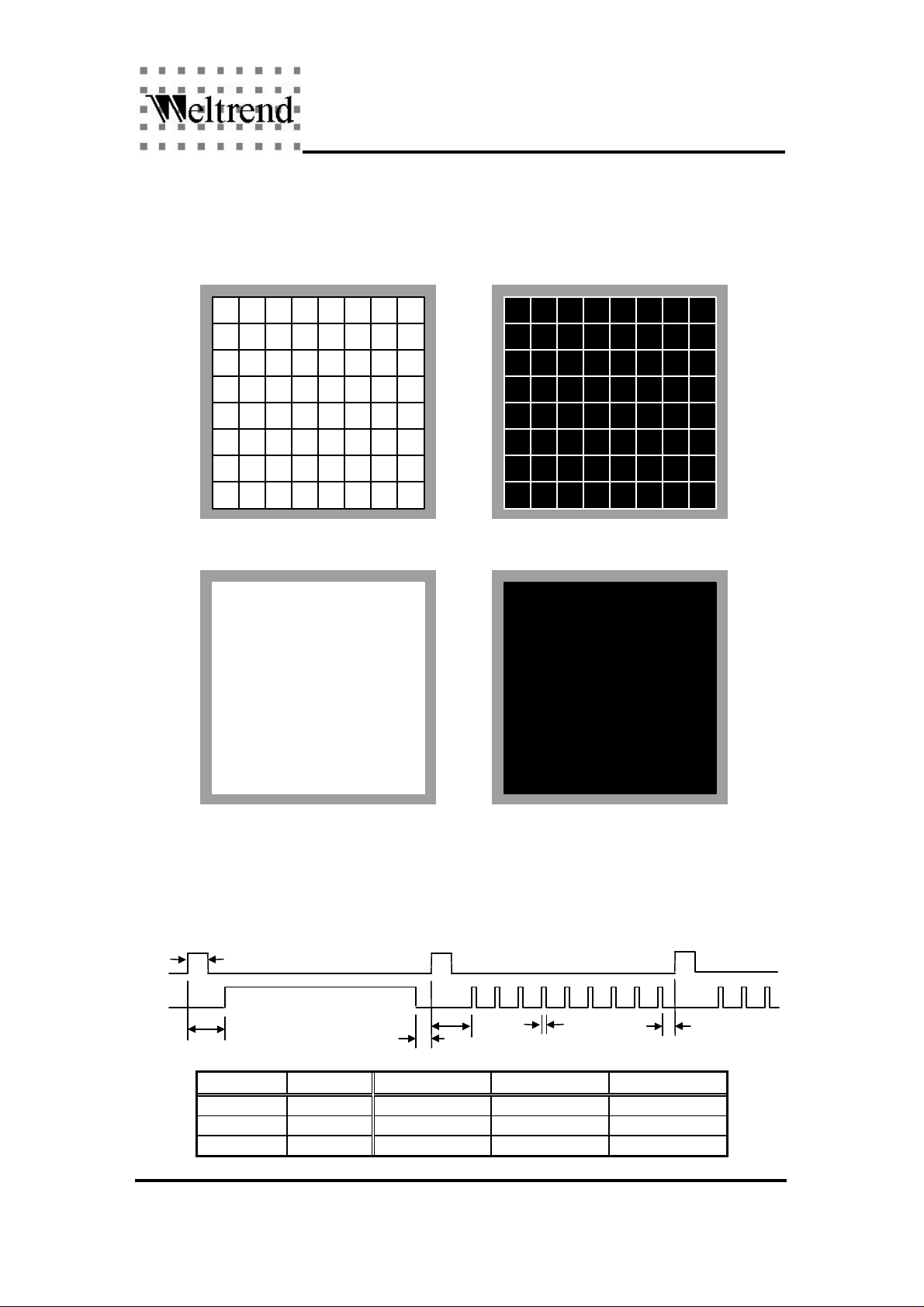
A self-test pattern signal comes out from pin PB3/PAT. It can generate a cross hatch picture, a
inverted cross hatch picture, a white picture or a black picture.
8 X 8 cross hatch Inverted 8 X 8 cross hatch
White Picture
Black Picture
The test pattern signal is generated when SELF and ENPAT are both set to “1”. This vedio signal
will synchronize to the free-running Hsync and Vsync, no matter which frequency is chosen. The
following diagram shows the timing relationship of cross hatch picture.
HSO
PAT
T
T
1
2
HSO VSO T
31.1kHz 60.8Hz 6us 1us 62.5ns
47.9kHz 74.9Hz 5.125us 0.625us 62.5ns
64kHz 62.5Hz 3.625us 0.875us 62.5ns
Weltrend Semiconductor, Inc.
T
1
1
T
3
T
2
T
2
T
3
10
Page 11
WT6018
Digital Monitor Controller
Ver. 1.41 Jul-31-1998
Half Frequency
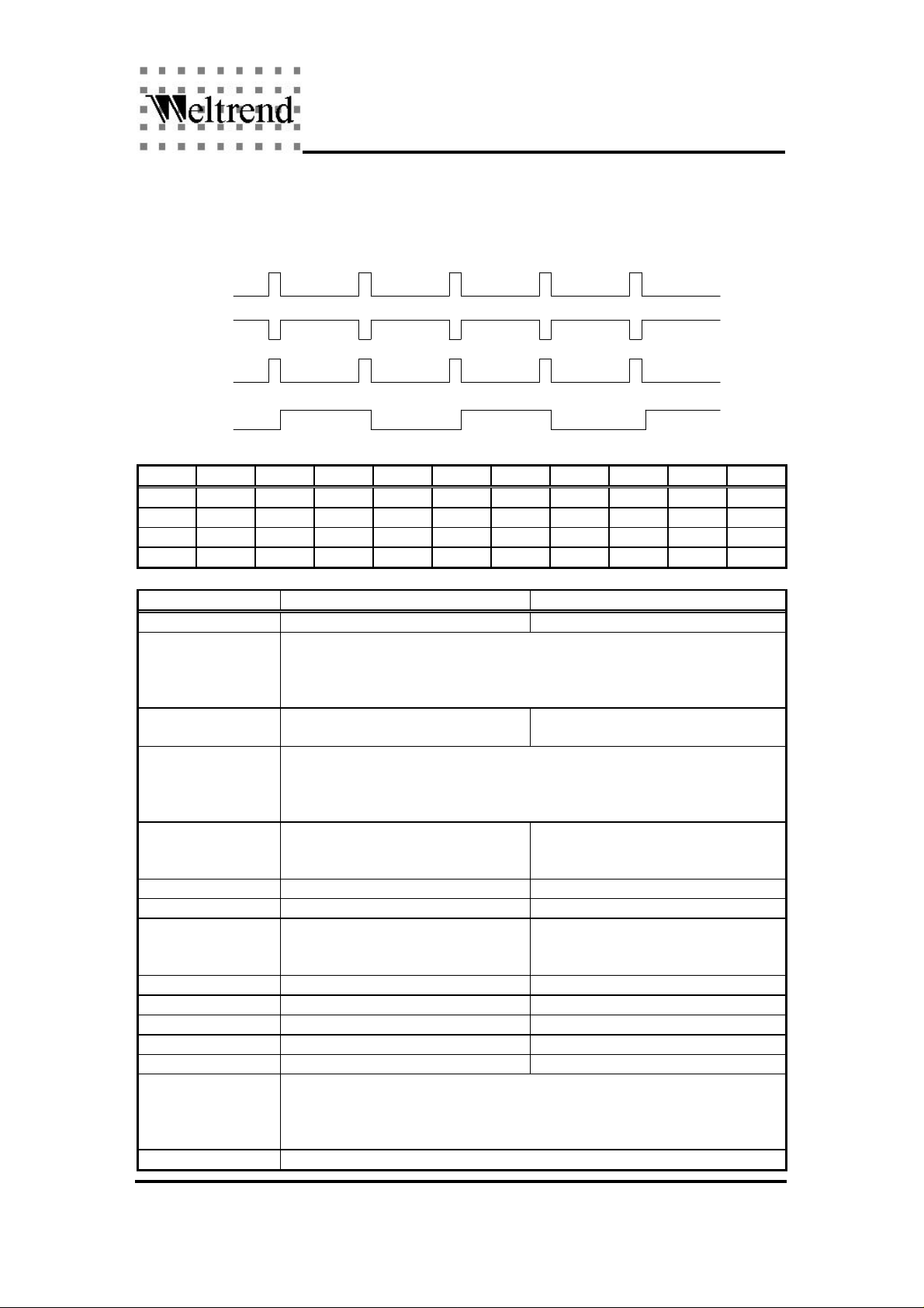
HLFO pin outputs same or half frequency from HLFI pin. The divide-by-2 operation is done on the falling
edge of HLFI pin when HALF bit is set. Polarity of HLFO is specified by HLFPO bit.
HLFI
HLFO
(HALF=0)
(HLFPO=0)
HLFO
(HALF=0)
(HLFPO=1)
HLFO
(HALF=1)
R/W Initial Bit7 Bit6 Bit5 Bit4 Bit3 Bit2 Bit1 Bit0
0016H W -- 0 0 ENPAT PAT1 PAT0 SELF H64K H48K
0016H R -- F9 F8 F7 F6 F5 F4 F3 F2
0017H W -- -- -- ENHLF HALF HLFPO H+V HOP VOP
0017H R 00H H/V -- H_POL V_POL OVF2 OVF1 F1 F0
Bit Name Bit value = “1” Bit value = “0”
ENPAT Pin PB3/PAT outputs test pattern. Pin PB3/PAT is I/O port.
PAT1,PAT0 If PAT1=0, PAT0=0, cross hatch picture.
If PAT1=0, PAT0=1, white picture.
If PAT1=1, PAT0=0, inverted cross hatch picture.
If PAT1=1, PAT0=1, black picture.
SELF HSO and VSO output free-running
HSO and VSO output sync signals.
frequency.
H64K, H48K H64K=“1”,H48K=“1” : Burn-in frequency=47.9kHz/74.9Hz
H64K=“0”,H48K=“1” : Burn-in frequency=47.9kHz/74.9Hz
H64K=“1”,H48K=“0” : Burn-in frequency=64kHz/62.5Hz
H64K=“0”,H48K=“0” : Burn-in frequency=31.1kHz/60.8Hz
ENHLF Pin PB1/HLFI is frequency input.
Pin PB0/HLFO is half frequency
Pin PB1/HLFI and PB0/HLFO is I/O
port.
output.
HALF HLFO outputs half frequency of HLFI. HLFO outputs same frequency of HLFI
HLFPO HLFO is positive polarity. HLFO is negative polarity.
H+V Enable H+V separation function.
Disable H+V separation.
This will select the sync signals come
from the sync separator.
HOP HSO pin is always positive polarity. HSO pin is always negative polarity.
VOP VSO pin is always positive polarity. VSO pin is always negative polarity.
H/V Counter stores horizontal frequency. Counter stores vertical frequency.
H_POL HSYNC input is positive polarity. HSYNC input is negative polarity.
V_POL VSYNC input is positive polarity. VSYNC input is negative polarity.
OVF2, OVF1 OVF2=“1”,OVF1=“0” : Counter overflowed twice.
OVF2=“0”,OVF1=“1” : Counter overflowed once.
OVF2=“0”,OVF1=“0” : No overflow.
OVF2=“1”,OVF1=“1” : No such condition.
F9-F0 Frequency counter value. (F9 is MSB)
Weltrend Semiconductor, Inc.
11
Page 12
WT6018
Digital Monitor Controller
Ver. 1.41 Jul-31-1998
DDC Interface
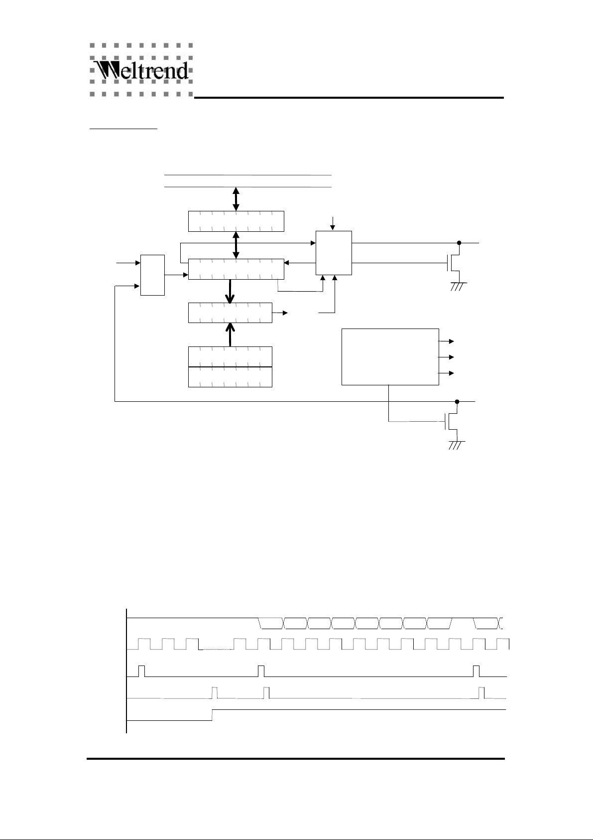
The DDC interface is a slave mode I2C interface with DDC1 function. It is fully compatible with
VEAS DDC1/2B standard. The functional block diagram is shown in the below.
Internal Data Bus
R/W
ADDR
ENACK
I/O
START/STOP Detect
Handshake Control
START
STOP
DDC2B
SCL
VSYNC
MUX
Data Buffer
Shift Register
Address Compare
MSB
1 10 0 0 0 0
Address Register
After power on or reset the DDC interface, it is in DDC1 state. The shift register shifts out data to
SDA pin on the rising edge of VSYNC clock. Data format is an 8-bit byte followed by a null bit. Most
significant bit (MSB) is transmitted first. Every time when the ninth bit has been transmitted, the shift
register will load a data byte from data buffer (REG#18H). After loading data to the shift register, the
data buffer becomes empty and generates an INT0 interrupt. So the program must write one data byte
into REG#18 every nine VSYNC clocks.
Since the default values of data buffer(REG#22) and shift register are FFH, the SDA pin outputs
high level if no data had been written into data buffer after power on reset. When program finished
initialization and set the IEN_D bit to "1", the INT0 will occur because the data buffer is empty. The
INT0 service routine should check the DDC2B bit is "0" and then writes the first EDID data byte into
data buffer. When the second INT0 occurs, the INT0 service routine writes the second EDID data byte
into data buffer and so on.
SDA
SDA
VSYNC
Load data to
shift register
INT0
IEN_D
1 2183
9 10 19
Weltrend Semiconductor, Inc.
Bit7 Bit6 Bit5 Bit4 Bit3 Bit2 Bit1 Bit0 Bit7
12
Page 13
WT6018
Digital Monitor Controller
Ver. 1.41 Jul-31-1998
If a low level occurs on the SCL pin in DDC1 state, the DDC interface will switch to DDC2B state
immediately and set the DDC2B bit to "1". No interrupt will be generated. But, if there is no valid
device address and it receives 128 VSYNC pulses while the SCL is high level, it will go back to
DDC1 state automatically. If it receives a valid device address, it will lock into DDC2B state and
disregard VSYNC.
In some case, program wants to go back DDC1 state, set RDDC bit in REG#1AH and reset it again.
This operation resets the DDC interface to the initial condition.
When it is in DDC2B state, the VSYNC clock is disregarded and the communication protocol
follows the DDC standard. The data format on SDA pin is:
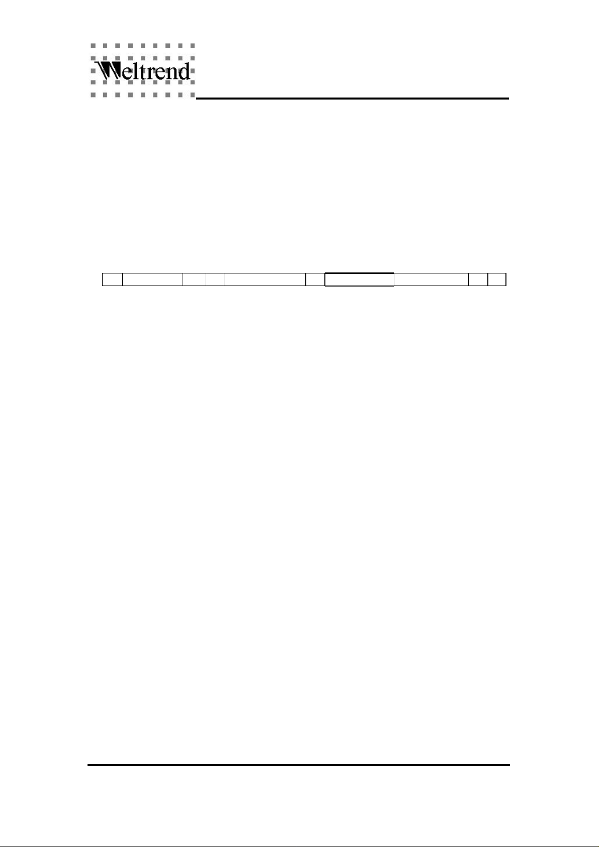
S Address R/W A D7,D6,...., D0 A D7,D6,...., D0 A P
S : Start condition. A falling edge occurs when SCL is high level.
P : Stop condition. A rising edge occurs when SCL is high level.
A : Acknowledge bit. “0” means acknowledge and “1” means non-acknowledge.
Address : 7-bit device address.
R/W : Read/Write control bit, "1" is read and "0" is write.
D7,D6,...., D0 : data byte.
The hardware operations in DDC2B state are :
(1) START/STOP detection
When the START condition is detected, the DDC interface is enabled and set START bit to "1".
When the STOP condition is detected, the DDC interface is disabled, set STOP bit to "1" and
generate INT0 interrupt.
The START bit is cleared when the following data byte received.
The STOP bit is cleared after writing REG#19H.
(2) Address Recognition
It contains two device addresses in WT6018. One fixed address (‘1010000’ ) is for EDID reading
and one programmable address (REG#19H) is for external control, such as auto alignment.
If the address is equal to "1010000", set ADDR bit to "0".
If the address is equal to the bit A6 to bit A0 (REG#19H), set ADDR bit to "1".
If the address is not equal to anyone above, the DDC interface will not response acknowledge.
The ADDR bit is updated when a new device address is received.
(3) Store R/W bit and decide the direction of SDA pin
The R/W bit on the SDA pin will be stored in the RW bit.
(4) Acknowledge bit control/detection
Acknowledge bit control in receive direction :
If ENACK=1 and address compare is true, response acknowledge (Acknowledge bit ="0").
If ENACK=0 or address compare is false, response non-acknowledge (Acknowledge bit ="1").
Acknowledge bit detect in transmit direction :
If the acknowledge bit is "1" , the DDC interface will be disabled and release the SDA pin.
If the acknowledge bit is "0" , the DDC interface keeps on communicating.
Weltrend Semiconductor, Inc.
13
Page 14
WT6018
Digital Monitor Controller
Ver. 1.41 Jul-31-1998
(5) Data bytes transmit/receive
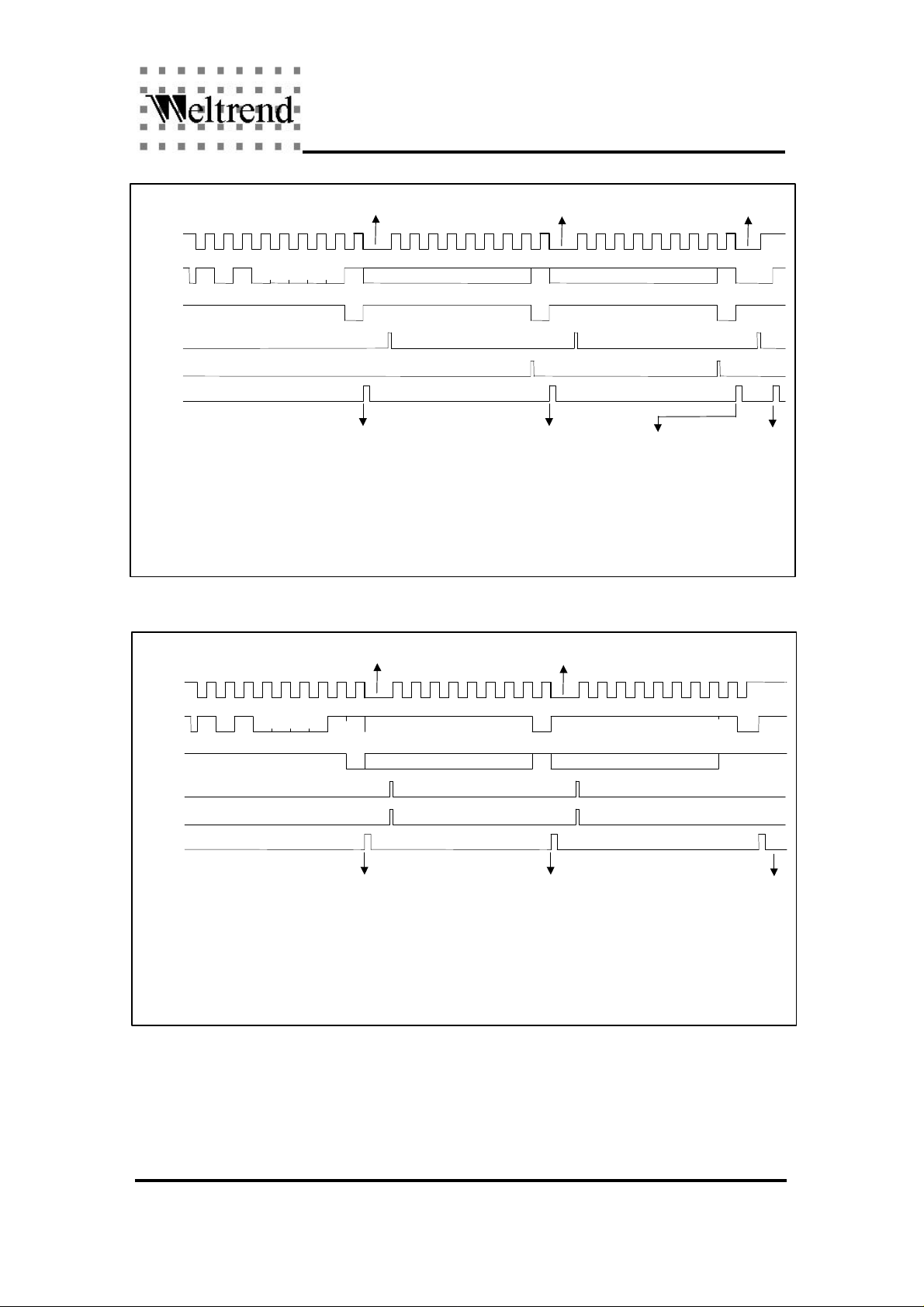
If the RW bit is "1", the shift register will load data from the data buffer (REG#18H) before the
data byte is transmitted and shift out data to the SDA pin before the rising edge of the SCL clock.
If the RW bit is "0", the shift register will shift in data on the rising edge of the SCL clock and the
whole data byte is latched to the data buffer(REG#18H).
(6) Handshaking procedure
The handshaking is done on the byte level. The DDC interface will hold the SCL pin low after the
acknowledge bit automatically. The bus master will be forced to wait until the WT6018 is ready for
the next byte transfer. To release the SCL pin, write REG#19H will release clear the wait state.
(7) Interrupt INT0
The DDC interface interrupt is enabled by setting the IEN_D bit in the REG#1AH.
Interrupt INT0 occurs when:
- Transmit buffer empty in DDC1 state.
The INT0 occurs when the shift register load data from data buffer.
Write REG#18H will clear the transmit buffer empty condition.
- Acknowledge is detected in DDC2B state.
The INT0 occurs on the falling edge of the SCL clock after the acknowledge had been
detected.
The SCL pin will be pulled low to force the bus master to wait until the service routine write
REG#19H.
- STOP condition occurs in DDC2B mode
Address R/W Initial Bit7 Bit6 Bit5 Bit4 Bit3 Bit2 Bit1 Bit0
0018H R/W FFH D7 D6 D5 D4 D3 D2 D1 D0
0019H R 40H DDC2B ADDR RW START STOP -- -- -0019H W A0H A6 A5 A4 A3 A2 A1 A0 ENACK
Bit Name Bit value = “1” Bit value = “0”
DDC2B DDC2B state. DDC1 state.
ADDR received address equals to the address
in REG#19H(W).
RW received R/W bit is ‘1’ . received R/W bit is ‘0’ .
START START condition is detected. No START condition is detected.
STOP STOP condition is detected. No STOP condition is detected.
ENACK Enable acknowledge. Disable acknowledge.
A6,A5, …., A0 7-bit slave address
D7,D6, …., D0 Data to be transmitted or received data.
received address equals to ‘1010000’ .
Weltrend Semiconductor, Inc.
14
Page 15
WT6018
Digital Monitor Controller
Ver. 1.41 Jul-31-1998
SCL
SDA
In
SDA
Out
Write REG#19H to release SCL
Shift register to data buffer
INT0
1 010
0 0 0
Pull low SCL
0
A A A
DDC2B=1
ADDR=0
R/W=0
START=1
STOP=0
Data Byte Data Byte
Pull low SCL
DDC2B=1
ADDR=0
R/W=0
START=0
STOP=0
DDC2B=1
ADDR=0
R/W=0
START=0
STOP=0
DDC2B state write timing
Pull low SCL
Pull low SCL
Pull low SCL
DDC2B=1
ADDR=0
R/W=0
START=0
STOP=1
SCL
SDA
In
SDA
Out
Write REG#19H to release SCL
Data buffer to shift reg
INT0
1 110 0 0 0 0
A
DDC2B=1
ADDR=0
R/W=1
START=1
STOP=0
Data Byte Data Byte
DDC2B state read timing
A
DDC2B=1
ADDR=0
R/W=1
START=0
STOP=0
N
DDC2B=1
ADDR=0
R/W=1
START=0
STOP=1
Weltrend Semiconductor, Inc.
15
Page 16
WT6018
Digital Monitor Controller
Ver. 1.41 Jul-31-1998
Interrupt Control
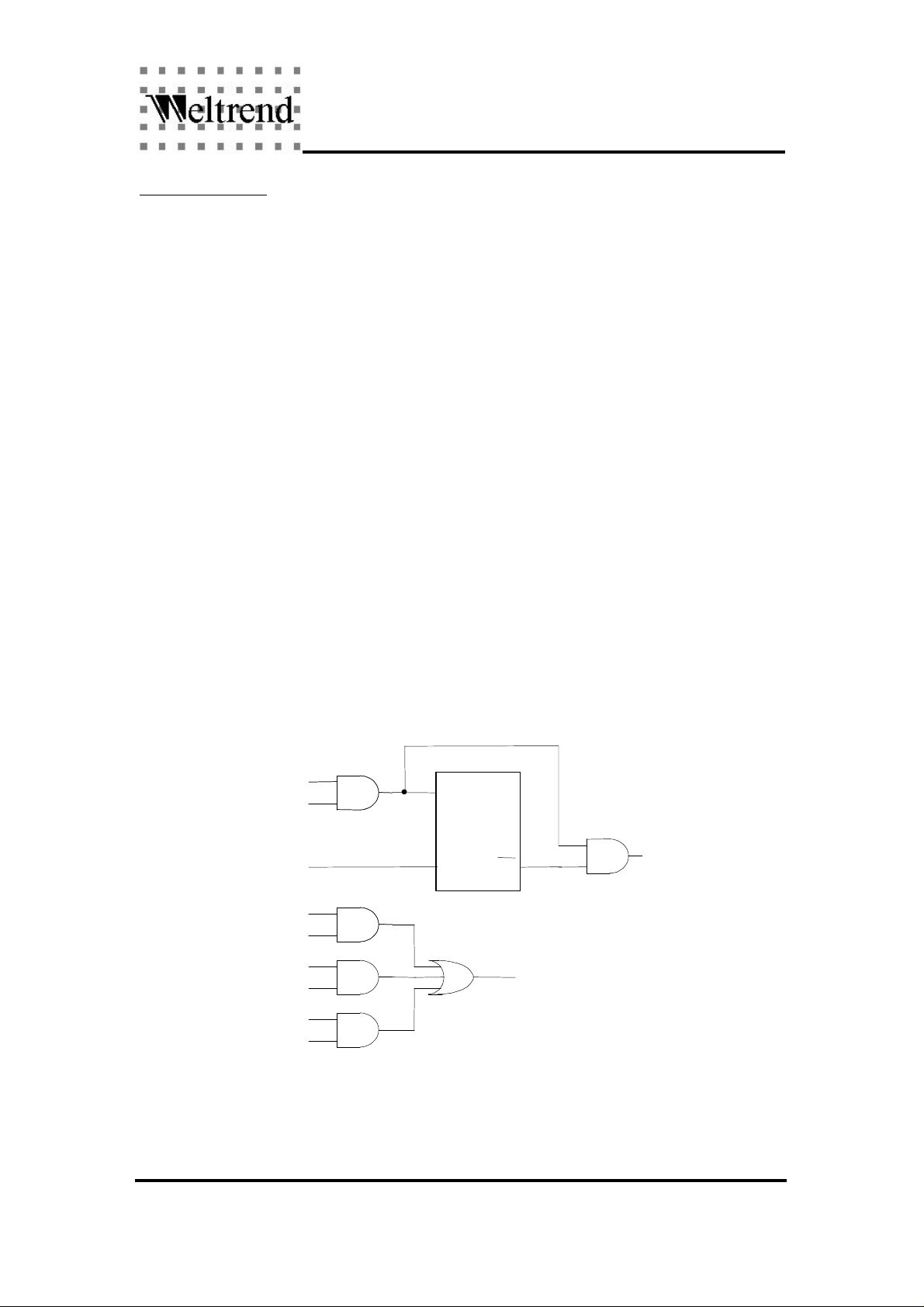
There are two interrupt sources : INT0 and INT1. INT0 has the higher priority.
Interrupt vector :
INT0 : FFFAH (low byte) and FFFBH (high byte).
INT1 : FFFEH (low byte) and FFFFH (high byte).
INT0 occurs when :
(1) data buffer empty in the DDC1 mode (DDC="1" and DDC2B="0").
(2) acknowledge or STOP condition is detected in the DDC2B mode (DDC="1" and DDC2B="0").
INT1 occurs when :
(1) a falling edge or a low level occurs on the /IRQ pin (EXT="1").
(2) the timer is time out (TIM="1").
(3) SYNC processor has a valid frequency (SYNC="1").
If H/V ="0" , it is vertical frequency ready.
If H/V ="1" , it is horizontal frequency ready.
INT0 is cleared when :
(1) writing the REG#18H in DDC1 state.
(2) writing the REG#19H in DDC2B state.
INT1 is cleared when :
(1) reading the REG#1AH if EXT="1".
(2) reading the REG#1BH if TIM="1".
(3) reading the REG#16H if SYNC="1".
IEN_D
DDC
IEN_X
IRQ
IEN_T
TOUT
IEN_S
FRDY
D
CK
Q
Q4MHz
INT0
INT1
Weltrend Semiconductor, Inc.
16
Page 17
WT6018
Digital Monitor Controller
Ver. 1.41 Jul-31-1998
Address R/W Initial Bit7 Bit6 Bit5 Bit4 Bit3 Bit2 Bit1 Bit0
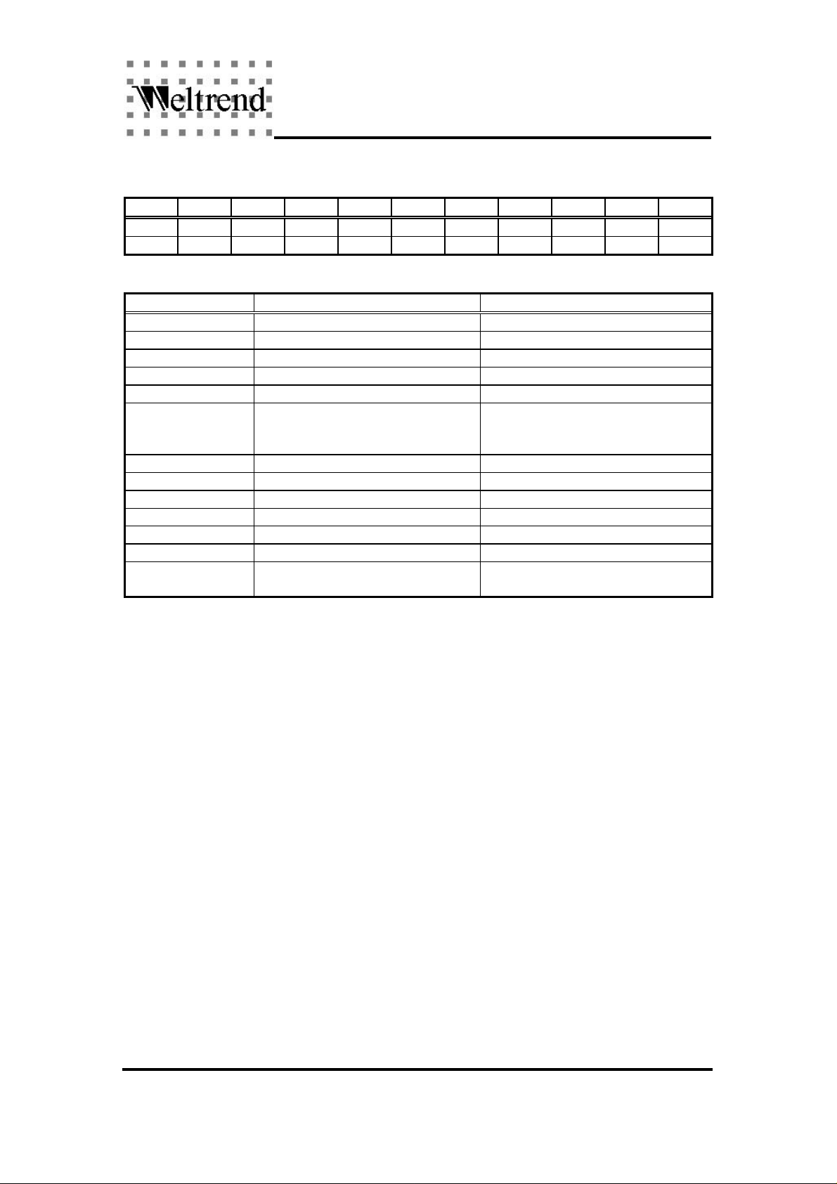
001AH W 00H IEN_X IEN_T IEN_S IEN_D EDGE RDDC 0 0
001AH R 00H EXT TIM SYNC DDC IRQ TOUT FRDY --
Bit Name Bit value = “1” Bit value = “0”
IEN_X Enable /IRQ pin interrupt. Disable /IRQ pin interrupt.
IEN_T Enable timer interrupt. Disable timer interrupt.
IEN_S Enable SYNC processor interrupt. Disable SYNC processor interrupt.
IEN_D Enable DDC interface interrupt. Disable DDC interface interrupt.
EDGE /IRQ pin interrupt is edge trigger. /IRQ pin interrupt is level trigger.
RDDC Reset DDC interface.
It will always reset DDC interface if
this bit keeps “1”.
EXT /IRQ pin interrupt occurs. No /IRQ pin interrupt.
TIM Timer interrupt occurs. No timer interrupt.
SYNC SYNC processor interrupt occurs. No SYNC processor interrupt.
DDC DDC interface interrupt occurs. No DDC interface interrupt.
IRQ /IRQ pin is low level /IRQ pin is high level
TOUT Timer is time-out. Timer is not time-out.
FRDY H/V frequency counter is ready.
The counter value is valid.
Clear the reset of DDC interface.
H/V frequency counter is not ready.
The counter value is invalid.
Weltrend Semiconductor, Inc.
17
Page 18
WT6018
Digital Monitor Controller
Ver. 1.41 Jul-31-1998
Timer
It is a 8-bit down counter and clock frequency is 976.5625Hz (period=1.024ms). The timer is
started by writing a value into REG#1BH. When the timer counts down to zero, the timer stops, sets
the TOUT bit and generates an INT1 interrupt (if the IEN_T bit is "1"). The TOUT bit will be cleared
after REG#1BH is read.
Watch-Dog Timer
The watch-dog timer is always enable after power is on. Software must clear the watch-dog timer
within every 524ms. If the watch-dog timer expired, It will cause the whole chip reset just like
external reset.
To clear the watch-dog timer, write any data to REG#1CH.
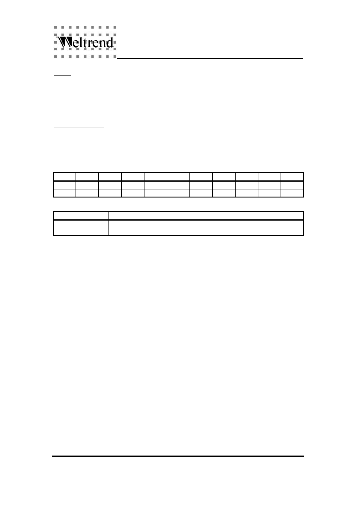
Address R/W Initial Bit7 Bit6 Bit5 Bit4 Bit3 Bit2 Bit1 Bit0
001BH R/W -- TM7 TM6 TM5 TM4 TM3 TM2 TM1 TM0
001CH W -- WDT WDT WDT WDT WDT WDT WDT WDT
Bit Name Bit value
TM7 to TM0 Timer value (0 - 255)
WDT Write any value to this register will reset the watchdog timer.
Weltrend Semiconductor, Inc.
18
Page 19
WT6018
Digital Monitor Controller
Ver. 1.41 Jul-31-1998
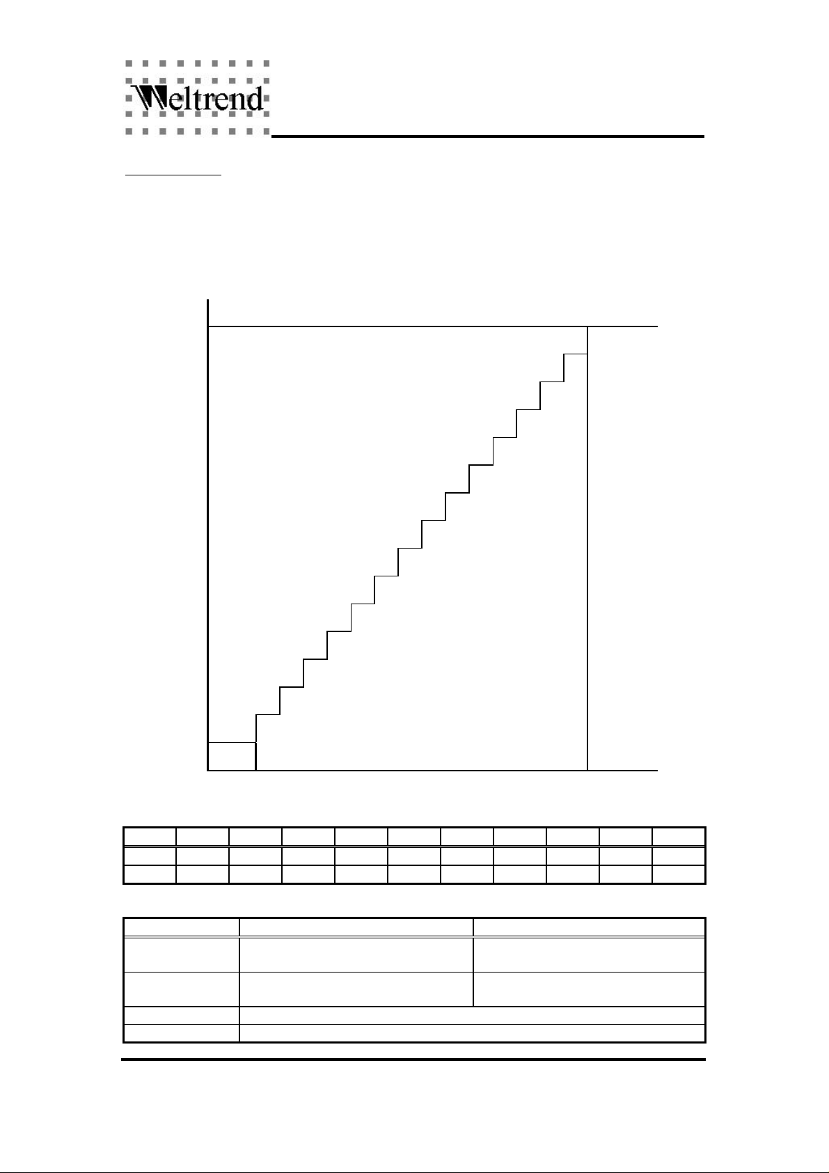
A/D Converter
Two 4-bit A/D converter inputs are shared with I/O port_C PC0 and PC1. Use ENAD1 bit and
ENAD0 bit to enable the corresponding A/D converter. The converted value is store in REG#20H.
Regardless of one A/D enabling or two A/D enabling ,the converted value is automatically updated at
2.048ms intervals.
4-bit data
1111
1110
1101
1100
1011
1010
1001
1000
0111
0110
0101
0100
0011
0010
0001
0000
Volt
0 0.75 4.02
Address R/W Initial Bit7 Bit6 Bit5 Bit4 Bit3 Bit2 Bit1 Bit0
0020H R -- AD13 AD12 AD11 AD10 AD03 AD02 AD01 AD00
0020H W 00H 0 0 0 0 0 0 ENAD1 ENAD0
Bit Name Bit value = “1” Bit value = “0”
ENAD1 Enable A/D converter 1.
Pin PC1 is the input of A/D converter 1.
ENAD0 Enable A/D converter 0.
Pin PC0 is the input of A/D converter 0.
Disable A/D converter 1.
Pin PC1 is I/O.
Disable A/D converter 0.
Pin PC0 is I/O.
AD13,…,AD10 4-bit data of A/D converter 1.
AD03,…,AD00 4-bit data of A/D converter 0.
Weltrend Semiconductor, Inc.
19
Page 20
WT6018
6
0
6
0
6
0
6
0
6
0
6
0
6
0
6
0
6
0
6
0
0
0
0
0
Digital Monitor Controller
Ver. 1.41 Jul-31-1998
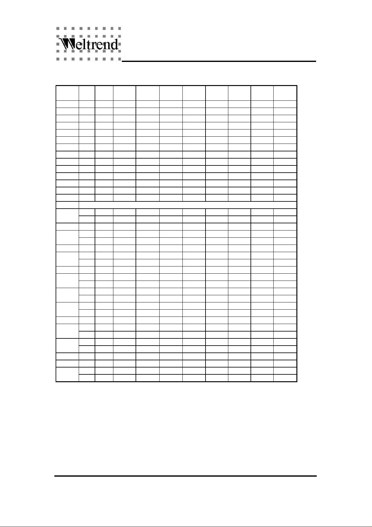
REGISTER MAP
Initial
R/W
Address
0000H R/W 80H DA07DA0
0001H R/W 80H DA17DA1
0002H R/W 80H DA27DA2
0003H R/W 80H DA37DA3
0004H R/W 80H DA47DA4
0005H R/W 80H DA57DA5
0006H R/W 80H DA67DA6
0007H R/W 80H DA77DA7
0008H R/W 80H DA87DA8
0009H R/W 80H DA97DA9
000AH R/W 80H DA107DA106DA105DA104DA103DA102DA101DA10
000BH R/W 80H DA117DA116DA115DA114DA113DA112DA111DA11
000CH R/W 80H DA127DA126DA125DA124DA123DA122DA121DA12
000DH R/W 80H DA137DA136DA135DA134DA133DA132DA131DA13
000EH Reserved
0010H W 00H EHO EVO EDA13 EDA12 EDA11 EDA10 EDA9 EDA8
0012H W 00H 0 PB6OE PB5OE PB4OE PB3OE PB2OE PB1OE PB0OE
0014H W 00H PC7OE PC6OE PC5OE PC4OE PC3OE PC2OE PC1OE PC0OE
0018H R/W FFH D7 D6 D5 D4 D3 D2 D1 D0
001BH R/W X TM7 TM6 TM5 TM4 TM3 TM2 TM1 TM0
001CH W X CWDT CWDT CWDT CWDT CWDT CWDT CWDT CWDT
value Bit7 Bit6 Bit5 Bit4 Bit3 Bit2 Bit1 Bit0
DA05DA04DA03DA02DA01DA0
DA15DA14DA13DA12DA11DA1
DA25DA24DA23DA22DA21DA2
DA35DA34DA33DA32DA31DA3
DA45DA44DA43DA42DA41DA4
DA55DA54DA53DA52DA51DA5
DA65DA64DA63DA62DA61DA6
DA75DA74DA73DA72DA71DA7
DA85DA84DA83DA82DA81DA8
DA95DA94DA93DA92DA91DA9
R X -- -- -- -- -- -- PD1R PD0R000FH
W 00H 0 0 0 ENPD PD1OE PD0OE PD1W PD0W
R X PA7R PA6R PA5R PA4R PA3R PA2R PA1R PA0R0011H
W FFH PA7W PA6W PA5W PA4W PA3W PA2W PA1W PA0W
R X -- PB6R PB5R PB4R PB3R PB2R PB1R PB0R0013H
W FFH 1 PB6W PB5W PB4W PB3W PB2W PB1W PB0W
R FFH PC7R PC6R PC5R PC4R PC3R PC2R PC1R PC0R0015H
W X PC7W PC6W PC5W PC4W PC3W PC2W PC1W PC0W
R X F9 F8 F7 F6 F5 F4 F3 F20016H
W 00H 0 0 ENPAT PAT1 PAT0 SELF H62K H48K
R 00H H/V -- H_POL V_POL OVF2 OVF1 F1 F00017H
W X 0 0 0 0 0 H+V HOP VOP
R 40H DDC2B ADDR RW START STOP -- -- --0019H
W A0H A6 A5 A4 A3 A2 A1 A0 ENACK
R 00H EXT TIM SYNC DDC IRQ TOUT FRDY --001AH
W 00H IEN_X IEN_T IEN_S IEN_D EDGE RDDC 0 0
R X AD13 AD12 AD11 AD10 AD03 AD02 AD01 AD000020H
W 00H 0 0 0 0 0 0 ENAD1 ENAD0
X : No default value.
-- : No function.
0 : Must write 0..
Weltrend Semiconductor, Inc.
20
Page 21
WT6018
Digital Monitor Controller
Ver. 1.41 Jul-31-1998
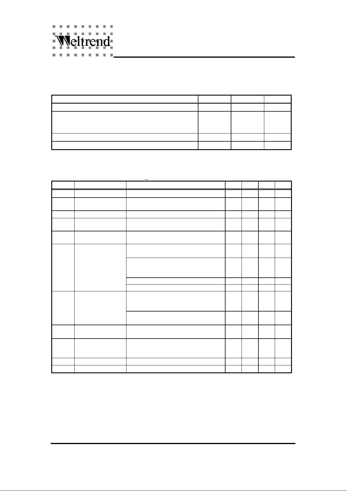
ELECTRICAL CHARACTERISTICS
Absolute Maximum Ratings
Parameter Min. Max Units
DC Supply Voltage (VDD) -0.3 7.0 V
Input and output voltage with respect to Ground
All pins except DA0 to DA7
DA0 to DA7
Storage temperature -65 150
Ambient temperature with power applied -10 70
* Note : Stresses above those listed may cause permanent damage to the device.
D.C. Characteristics ( VDD=5.0V + 5% , Ta=0 - 70 OC)
Symbol Parameter Condition Min. Typ. Max. Units
V
V
V
V
V
V
R
I
V
RESET
SIH
SIL
I
DD
DD
IH
IL
OH
OL
IL
PH
Supply Voltage 4.0 5 5.5 V
Input High Voltage All input pins (except HSYNC and VSYNC) 3.0 - VDD+
Input Low Voltage All input pins (except HSYNC and VSYNC) -0.3 - 1.5 V
Sync Input High
Voltage
Sync Input Low
Voltage
Output High Voltage
Output Low Voltage
Input Leakage Current SDA, SCL, HSYNC and VSYNC pins ( V
Pull High Resistance VIN=0.8V
Operating Current No load - 3 20 mA
Reset Voltage /RESET pin 3.8 4.0 4.2 V
HSYNC and VSYNC pin 2.0 - VDD+
HSYNC and VSYNC pin -0.3 - 0.8 V
IOH= -100uA
PA0-PA7 pins
IOH= -6mA
PB0-PB6, PC0-PC7, PD0, PD1, DA8-DA13,
HSO, VSO and HSO pins
DA0-DA7 pins (external voltage) - - 10.5 V
SCL and SDA pins (open drain) - - 5.5 V
IOL= 5mA
PA0-PA7, PB0-PB6, PD0-1, DA0-DA13,
SCL, SDA, VSO and HSO pins
IOL= 10mA
PC0-PC7 pins
= 0 to 5V)
PA0-PA7, PB0-PB6, PC0-PC7, /RESET and
/IRQ pins
-0.3
-0.3
VDD+0.3
11.5V
3.5 - - V
3.5 - - V
- - 0.4 VV
- - 0.4 V
-10 - 10 uA
IN
16 22 28 Kohm
0.3
0.3
V
V
o
C
o
C
V
V
Weltrend Semiconductor, Inc.
21
Page 22
WT6018
Digital Monitor Controller
Ver. 1.41 Jul-31-1998
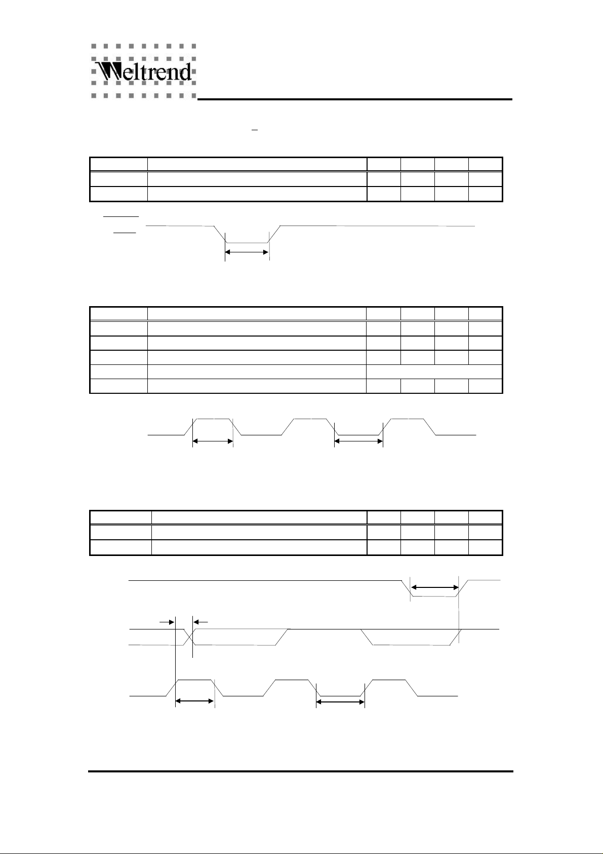
A.C. Characteristics ( VDD=5.0V + 5%, fosc=8MHz, Ta=0 - 70OC)
RESET and IRQ Timing
Symbol Parameter Min. Typ. Max. Units
t
LOW,RES
t
LOW,IRQ
RESET
IRQ
SYNC Processor Timing
Symbol Parameter Min. Typ. Max. Units
t
HIGH,SYNC
t
LOW,SYNC
t
FPW,HSO
t
FPW,VSO
t
IPW,HSO
/RESET pin low pulse 250 - - ns
/IRQ low pulse (level trigger) 250 - - ns
t
LOW,RES
t
HIGH,IRQ
HSYNC and VSYNC high time 250 - - ns
HSYNC and VSYNC low time 250 - - ns
Self generated free-running HSO pulse width - 2 - us
Self generated free-running VSO pulse width 4 x HSO period
Inserted Hsync pulse width (composite sync input) - 2 - us
HSYNC
VSYNC
t
HIGH,SYNC
t
LOW,SYNC
DDC1 Timing
Symbol Parameter Min. Typ. Max. Units
t
VAA,DDC1
t
SCL
SDA
MT
SDA output valid from VSYNC rising edge 125 - 500 ns
Mode transition time (DDC1 to DDC2B) - - 500 ns
t
MT
t
VAA,DDC1
Bit 0 (LSB)
Bit 7 (MSB)Null Bit
VSYNC
t
HIGH,SYNC
t
LOW,SYNC
Weltrend Semiconductor, Inc.
22
Page 23
WT6018
Digital Monitor Controller
Ver. 1.41 Jul-31-1998
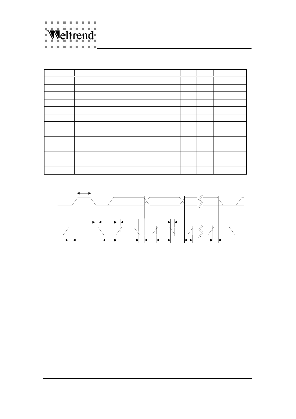
DDC2B Timing
Symbol Parameter Min. Typ. Max. Units
f
SCL
t
BF
t
HD,START
t
SU,START
t
HIGH,SCL
t
LOW,SCL
HD,DATA
SU,DATA
t
RISE
t
FALL
t
SU,STOP
SCL input clock frequency 0 - 100 kHz
Bus free time 2 - - us
Hold time for START condition 1 - - us
Set-up time for START condition 1 - - us
SCL clock high time 1 - - us
SCL clock low time 1 - - us
Hold time for DATA input 0 - - nst
Hold time for DATA output 250 - - ns
Set-up time for DATA input 250 - - nst
Set-up time for DATA output 500 - - ns
SCL and SDA rise time - - 1 us
SCL and SDA fall time - - 300 ns
Set-up time for STOP condition 4 - - us
SDA
SCL
t
SU,STOP
t
BF
t
HD,START
t
LOW,SCL
t
RISE
t
HD,DATA
t
HIGH,SCL
t
FALL
t
SU,DATA
t
SU,START
Weltrend Semiconductor, Inc.
23
 Loading...