

Page 1
! 3-Termainal Regulators
! Output Current Up to 1.5 A
! No External Components
! Internal Thermal Overload Protection
! High Power Dissipation Capability
! Internal Shot-Circuit Current Limiting
! Output Transistor Safe-Area
Compensation
DESCRIPTION
This series of fixed-voltage monolithic integrated-circuit
voltage regulators designed for a wide range of
applications. These applications include on-card
regulation for elimination of noise and distribution
problems associated with single-point regulation. Each
of these regulators can deliver up to 1.5 amperes of
output current. The internal current limiting and thermal
shutdown features of these regulators make them
essentially immune to overload.
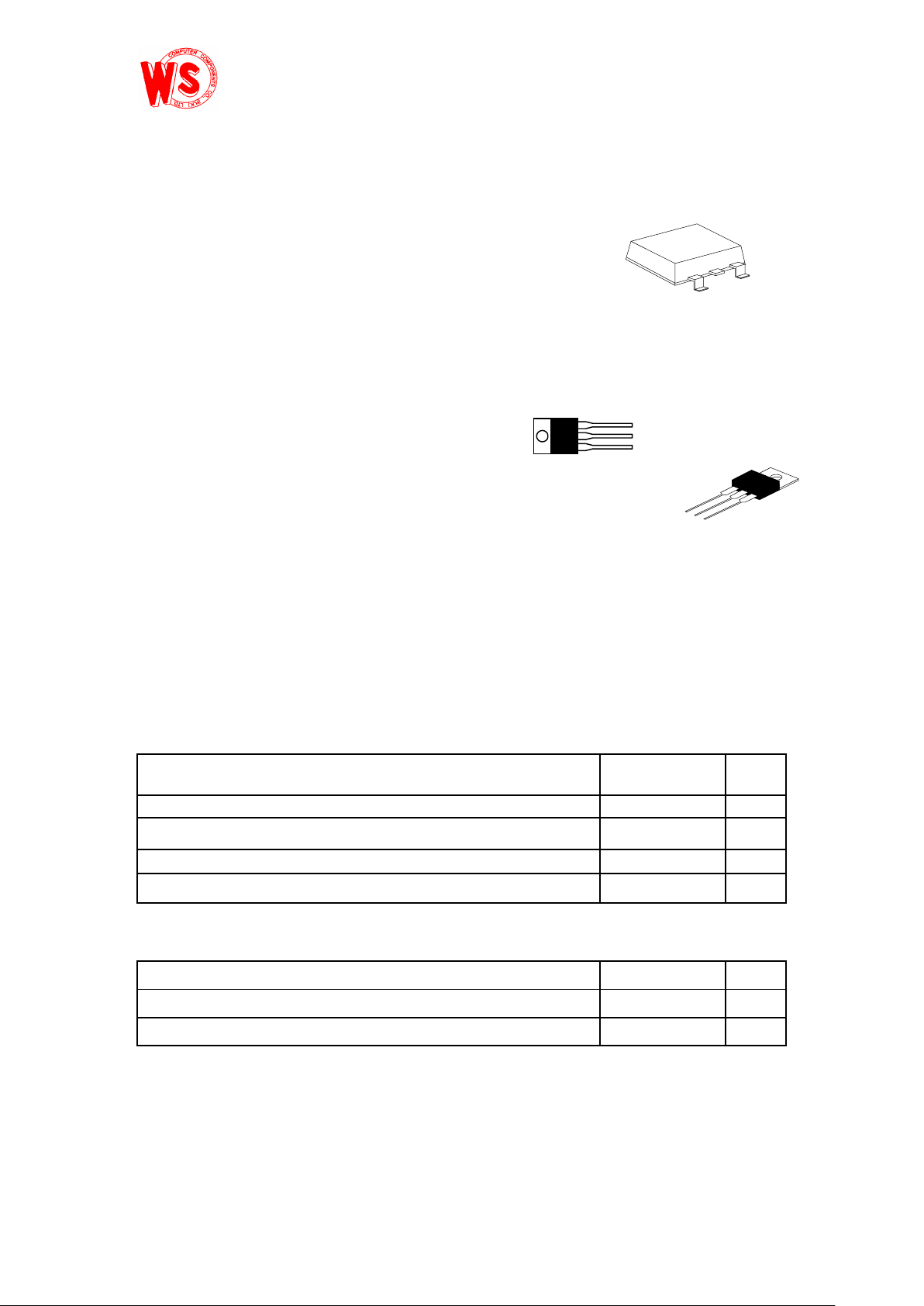
ABSOLUTE MAXIMUM RATINGS OVER OPERATING TENPERATURE
RANGE (UNLESS OTHERWISE NOTE
WS7805 PARAMETER UNIT
Input voltage, V
I
35 V
Continuous total dissipati on at 25℃ free-air temperature
2W
Lead temperature 1.6mm (1/16 inch) from case 10 seconds 260
℃
Storage temperature range, T
stg
-65 to 150
℃
RECOMMEMDED OPERATING CONDITIONS
MIN MAX UNIT
Input voltage, V
I
7
Output current, I
O
1.5 A
Operating virtual junction temperature, T
J
070
℃
I
C
O
(TO-252)
Wing Shing Computer Components Co., (H.K.)Ltd. Tel:(852)2341 9276 Fax:(852)2797 8153
Homepage: http://www.wingshing.com E-mail: [email protected]
Page 2
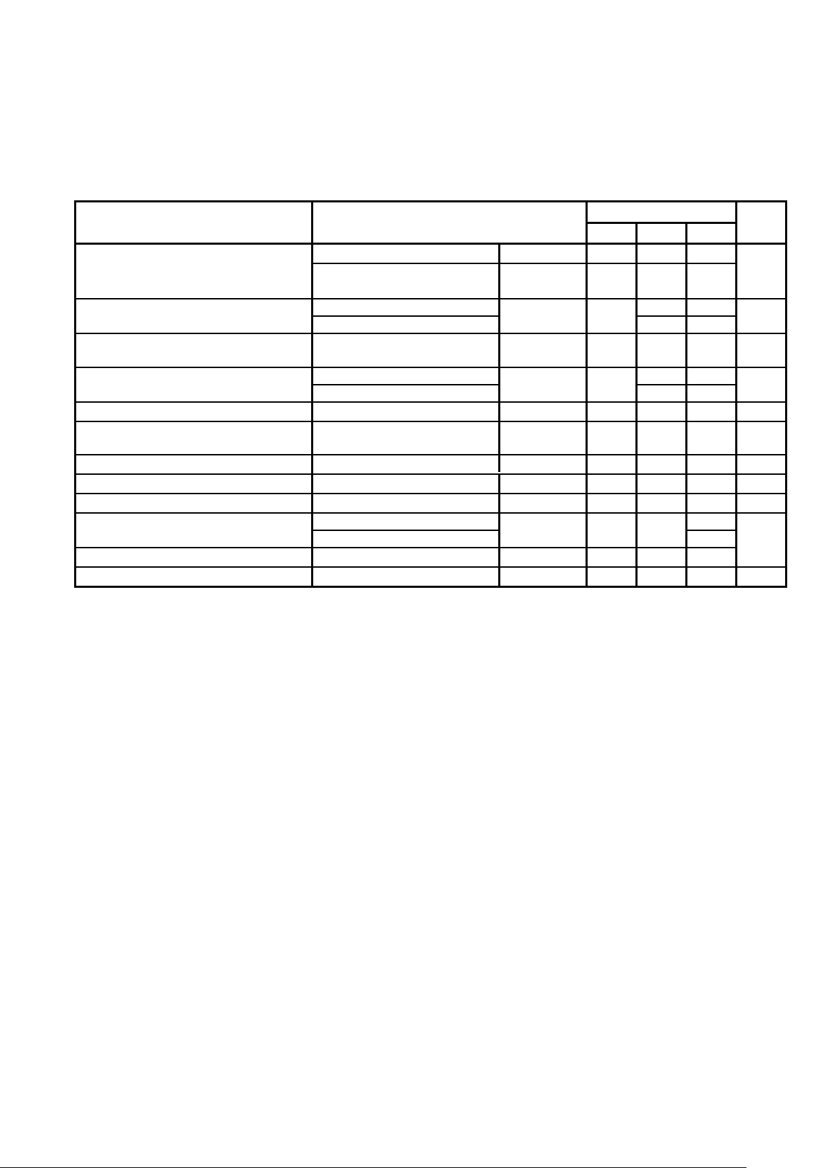
WS7805 Electrical characteristics at specified virtual junction
temperature, V
I
=10V, IO=500mA (unless otherwise noted)
WS7805
PARAMETER TEST CONDITIONS
MIN TYP MAX
UNIT
25℃
4.8 5 5.2
Output voltage
I
O
=5mA to1A,
V
I
=7V to 20V, P≦15W
0℃ to 70℃
4.75 5 5.25
V
VI=7V to 25V 3 100
Input regulation
V
I
=8V to12V
25℃
150
Ripple rejection
V
I
=8V to18V
F=120H
Z
0℃ to 70℃
62 78 dB
IO=5mA to 1.5A 15 100
Output regulation
I
O
=250mA to 750mA
25℃
550
mV
Output resistance F=1KH
Z
0℃ to 70℃
0.017
Ω
Temperature coefficient of output
voltage
I
O
=5mA
0℃ to 70℃
-1.1
mV/℃
Output noise voltage F=10HZ to 100 kHz
25℃
40
μV
Dropout voltage IO=1A
25℃
2.0 V
Bias current
25℃
4.2 8 mA
VI=7V to 25V 1.3
Bias current change
I
O
=5mA to 1A
0℃ to 70℃
0.5
Short-circuit output current
25℃
750
Peak output current
25℃
2.2 A
Page 3
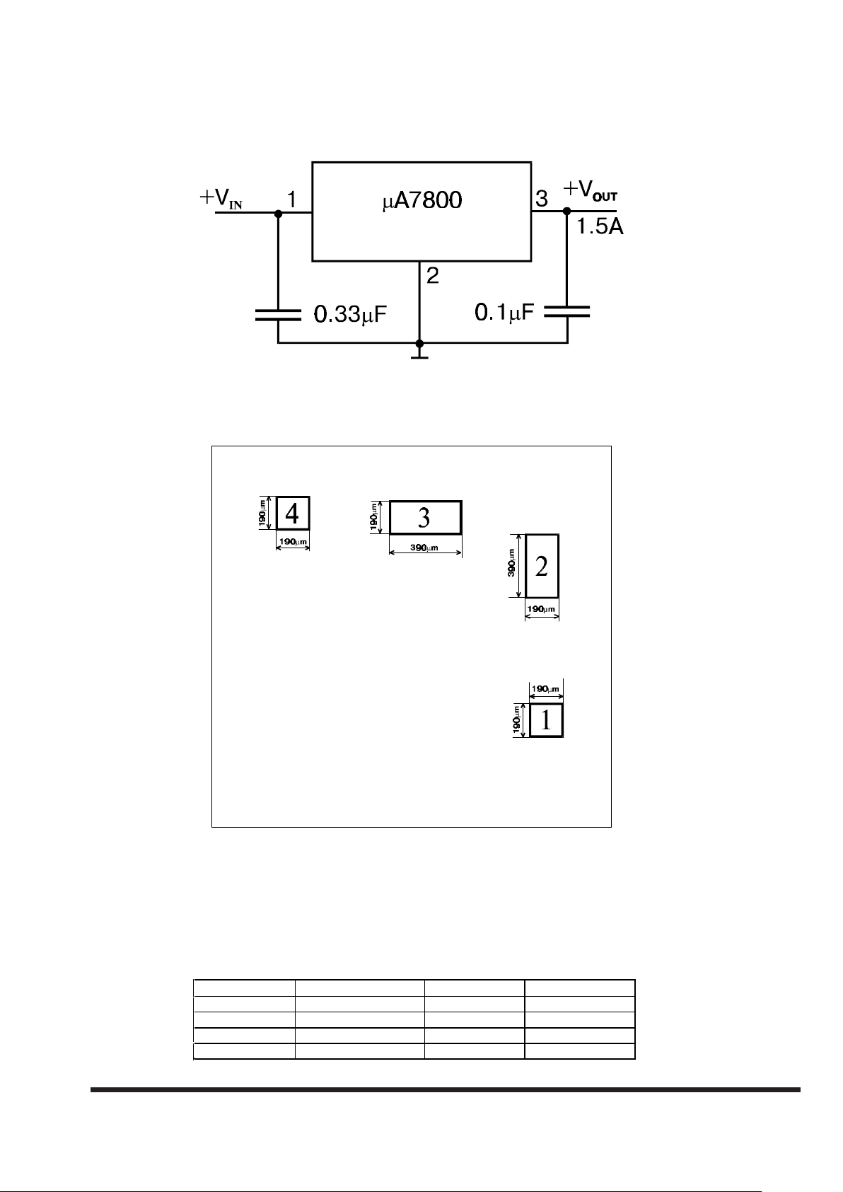
Fig. 1. Positive Regulator
Pad Location
Chip size 2.0 x 2.0 mm
• Metallization
Top Al
Back no
• Die Thickness 460±20µm
Pad Location Coordinates
Pad N Pad Name
X (µm) Y (µm)
1 Ground 1710 130
2 Input 1590 815
3 Output 690 1685
4 Output 190 1710
 Loading...