

Page 1
Features
3 Digit LCD/LED Display A/D
Converters
1
2
/
WS7106 / WS7107
WS7107CPL
0 to70
40Ld PDIP
E40.6
WS7106CPL
0 to 70
40Ld PDIP
E40.6
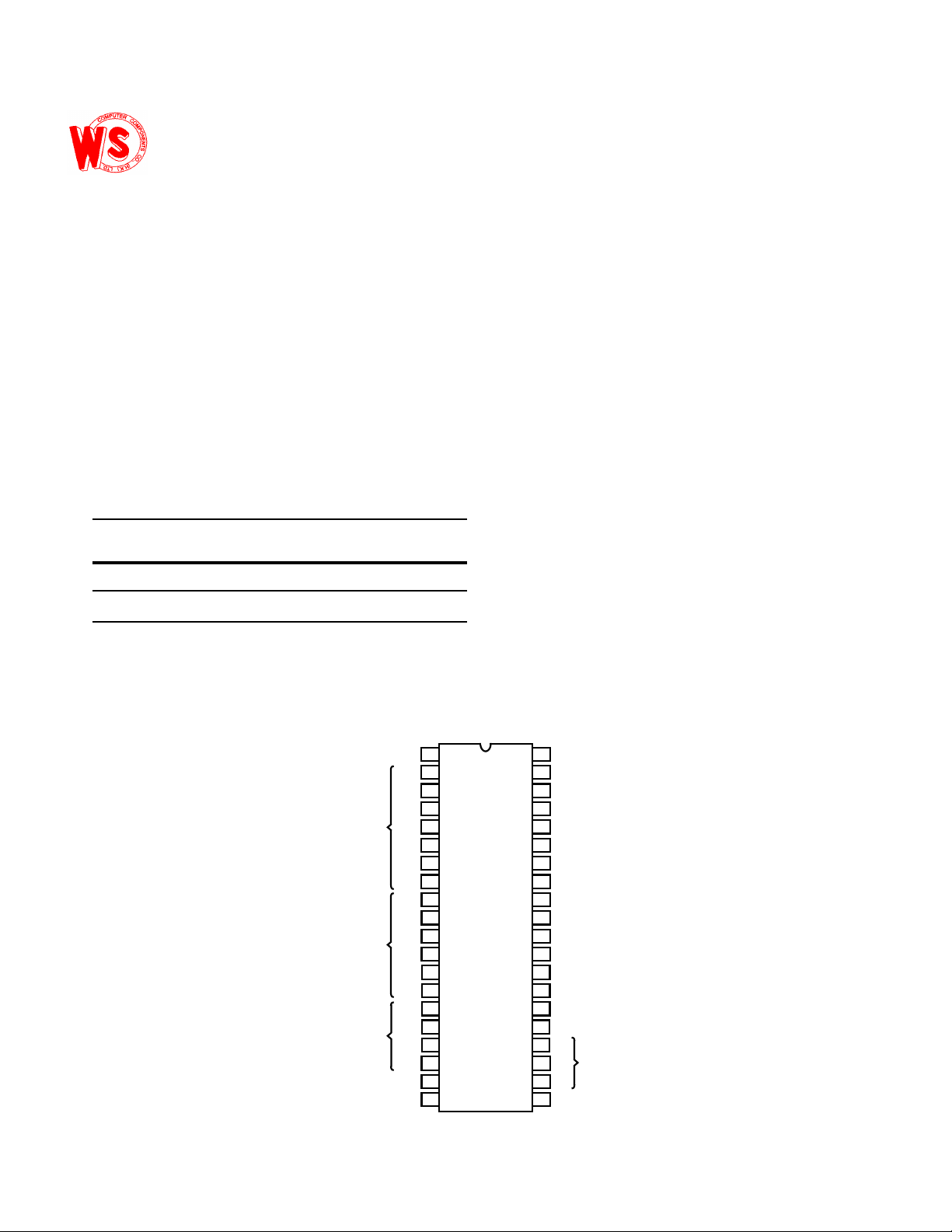
Pinouts
WS7106CPL (PDIP)
WS7107CPL (PDIP)
- LCD WS7106, LED WS7107
The WS7106 and WS7107
The WS7106
WS
The WS7106 and WS
True differential
inputs and reference are useful in all systems, but give the
desiger an uncommon advantage when measuring load
cells, strain gauges and other bridge type transducers.
Finally, the true economy of single power supply operation
(WS7106), enables a high performance panel meter to built
with the addition of only 10 passive compoents and a disply.
• True Differential Input and Reference, Direct Display
Drive
• On Chip Clock and Reference
• No Additional Active Circuits Required
Guaranteed Zero Reading for 0V Input on All Scales
True Polarity at Zero for Precise Null Detection
Typically Less Than 10mW
•
•
•Low Noise - Less Than 15µV
•Low Power Dissipation -
Ordering Information
TEMP.
PART NO.
RANGE (oC) PACKAGE PKG. NO.
P-P
Description
power, 3
1
/2digit A/D converters. Included are seven seg-
ment decoders, display drivers, a reference, and a clock.
isdesignedtointerfacewithaliquidcrystaldis-
play (LCD) and includes a multiplexed backplane drive; the
7107willdirectlydriveaninstrumentsizelightemitting
diode (LED) display.
7107bringtogetheracombinationof
highaccuracy,versatility,andtrueeconomy.
arehighperformance,low
(10’ s)
(100’ s)
(1000) AB4
(MINUS)
Wing Shing Computer Components Co., (H.K.)Ltd. Tel:(852)2341 9276 Fax:(852)2797 8153
Homepage: http://www.wingshing.com E-mail: [email protected]
(1’ s)
V+
D1
C1
B1
A1
F1
G1
E1
D2
C2
B2
A2
F2
E2
D3
B3
F3
E3
POL
1
2
3
4
5
6
7
8
9
10
11
12
13
14
15
16
17
18
19
20
40
39
38
37
36
35
34
33
32
31
30
29
28
27
26
25
24
23
22
21
OSC 1
OSC 2
OSC 3
TEST
REF HI
REF LO
+
C
REF
-
C
REF
COMMON
IN HI
IN LO
A-Z
BUFF
INT
VG2 (10’s)
C3
(100’ s)
A3
G3
BP/GND
Page 2
Absolute Maximum Ratings Thermal Information
2
WS7106/WS710
Supply Voltage Thermal Resistance (typical, Note 2) θJA(℃/W)
WS7106, V+ to V-…………………………….15v PDIP Package……………………………………………. …… ………… 50
WS7107, V+ to GND…………………….……6V Maximum Junction Temperature…………………………………….. ………150℃
WS7107, V_ to GND……………………. ….-9V Maximum Storage Temperature Range………………….………..-65℃ to 150℃
Analog Input Voltage (Either Input) (Note 1)V+ to VReference Input Voltage (Either Input)V+ to VClock Input
WS7106TEST to V+
WS7107GND to V+
Operating Conditions
Temperature Range…………………………0℃ to 70℃
CAUTION: Stresses above those listed in “absolute Maximum Ratings” may cause permanent damage to the device. This is a stress only rating and operation
Of the device at these or any other conditions above those indicated in the operational sections of this specification is not implied.
Notes:
1. Input voltages may exceed the supply voltages provided the input current is limited to ±100µA
2. Θ
Is measured with the component mounted on an evaluation PC on board in fee air.
JA
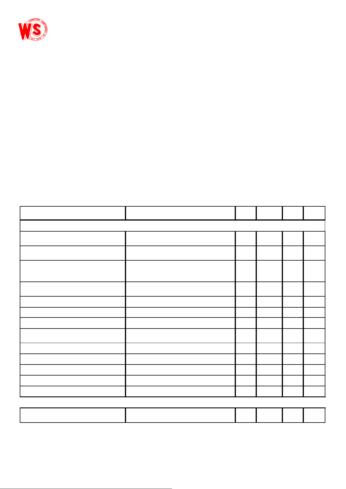
Electrical specifications
PARAMETER
(Note 3)
TEST CONDITIONS MIN TYP MAX UNIT
SYSTEM PERFORMACE
Zero Input Reading VIN=0.0V, FULL Scale = 200mV -000.0 ±000.0 +000.0
Ratiometric Reading VIN = V
-V
Rollover Error
Difference in Reading for Equal Positive and
, V
REF
=+VIN=200mV
IN
= 100mV 999 999/1000 1000
REF
-1 0.2 +1 Counts
Digital
Reading
Digital
Reading
Negative Inputs Near Full Scale
Linearity
Common Mode Rejection Ratio V
Full Scale = 200mV or Full Scale = 2V Maximum
Deviation from Best Straight Line Fit (note 6)
= 1V, VIN = 0V, Full Scale = 200mv(Note 6) - 50 - μV/V
CM
-1 0.2 +1 Counts
End Power Supply Character V+ Supply Current VIN = 0 (Does Not Include LED Current for WS7107 - 0.5 1.8 mA
End Power Supply Character V- Supply Current WS7107 Only - 0.5 1.8 mA
COMMON Pin Analog Common Voltage
25kΩ Between Common and Positive Supply (With
Respect to + Supply)
2.4 3.0 3.2 V
Noise (PK-PK Value not exceeded 95% of time) VIN=0V Full Scale=200mV 15 uV
Input Leakage Current VIN=0V 1 10 pA
P-P
Analog COMMON Temperature Coefficient 25K between Common and V+ 0℃-70℃ 60 75 ppm/℃
Scale Factor Temperature Coefficient VIN=199mV 0℃-70℃Ext. ref. 0ppm/℃ 60 75 ppm/℃
Zero Reading Drift VIN=0℃V-70℃ 0.2 1 uV/℃
DISPLAY DRIVER WS7106 ONLY
Peak-to-Peak Segment Drive Voltage
Peak-to-Peak Backplane Drive Voltage
V+ = to V- = 9V (Note 5) 4 5 6 V
Page 3
Electrical Specifications (Continued)
WS7106 / WS7107
WS7107 ONLY
2. Back plane drive is in phase with segment drive for 'off' segment, 180 degrees out of phase for 'on' segment. Frequency is 20
times conversion rate. Average DC component is less than 50mV
WS7106
WS7107
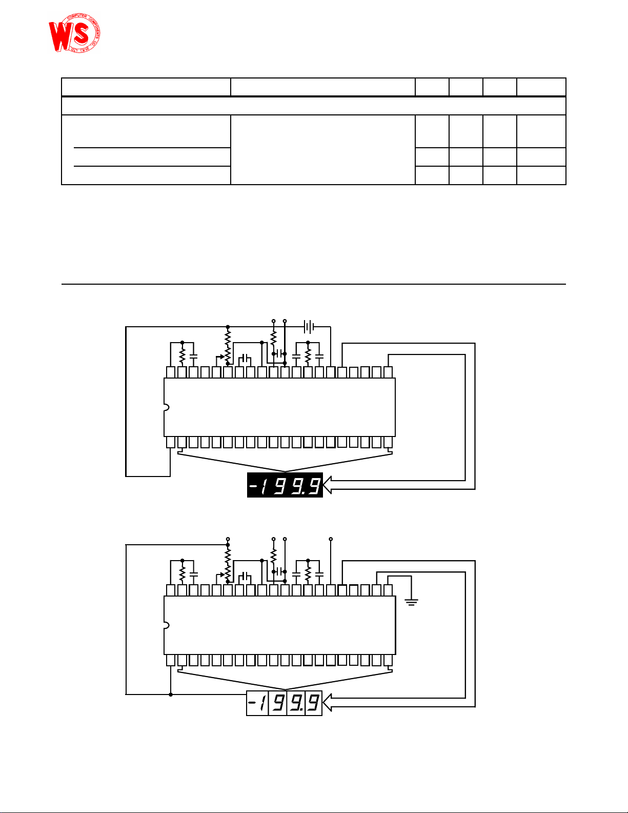
FIGURE 1. WS
FIGURE 2. WS
3
DISPLAY DRIVER
(Note 1)
1.
3. Not tested, Quaranteed by design.
PARAMETER TEST CONDITIONS MIN TYP MAX UNIT
Segment Sinking Current V+ = 5V, Segment Voltage = 3V
(Except Pins 19 and 20) 58- mA
Pin 19 Only 10 16 - mA
Pin 20 Only 47- mA
NOTES:
3.Dissipation rating assumes device is mounted with all leads soldered to printed circuit board.
Typical Applications and Test Circuits
+ -
R
C
+
C
REF
5
1
-
REF
COM
C
DISPLAY
R
1
R
R
3
4039383736353433323130
OSC 1
OSC 2
V+
D1C1B1
123456789
4
C
4
TEST
OSC 3
REF HI
REF LO
A1F1G1E1D2C2B2
IN
C
5
C
2
IN HI
IN LO
101112
9V
+
-
R
2
C
3
28
29
27262524232221
V-
INT
A-Z
BUFF
F2
E2
A2
D3
13
14151617181920
DISPLAY
G2
B3
C1 = 0.1µF
= 0.47µF
C
2
= 0.22µF
C
C3
A3
G3
BP
F3
E3
AB4
POL
3
C
= 100pF
4
= 0.02µF
C
5
= 24kΩ
R
1
R
= 47kΩ
2
= 100kΩ
R
3
= 1kΩ
R
4
R
= 1MΩ
5
7106TESTCIRCUITANDTYPICALAPPLICATIONWITHLCDDISPLAYCOMPONENTSSELECTEDFOR200mV
FULL SCALE
+5V -5V
R
1
C
R
C
4
OSC 3
TEST
4
REF HI
+
C
REF LO
F1
G1
R
3
4039383736353433323130
OSC 1
OSC 2
V+D1C1B1A1
123456789
+ -
IN
R
5
C
5
R
2
COM
DISPLAY
C
IN HI
IN LO
101112
1
-
REF
REF
C
E1D2C2B2A2F2E2D3B3F3E3
C
2
3
28
29
27262524232221
INT
A-Z
BUFF
13
14151617181920
V-
DISPLAY
G2
C1 = 0.1µF
= 0.47µF
C
2
= 0.22µF
C
C3
A3
G3
GND
AB4
POL
3
C
= 100pF
4
= 0.02µF
C
5
= 24kΩ
R
1
R
= 47kΩ
2
= 100kΩ
R
3
= 1kΩ
R
4
R
= 1MΩ
5
7107TESTCIRCUITANDTYPICALAPPLICATIONWITHLEDDISPLAYCOMPONENTSSELECTEDFOR200mV
FULL SCALE
Page 4
Design Information Summary Sheet
WS7106 / WS7107
WS
WS7106 DISPLAY: LCD
WS7107 POWER SUPPLY: DUAL +5.0V
_
WS7107 DISPLAY: LED
4
• OSCILLATOR FREQUENCY
= 0.45/RC
f
OSC
C
> 50pF; R
OSC
f
(Typ) = 48kHz
OSC
• OSCILLATOR PERIOD
= RC/0.45
t
OSC
• INTEGRATION CLOCK FREQUENCY
CLOCK
= f
OSC
f
• INTEGRATION PERIOD
= 1000 x (4/f
t
INT
• 60/50Hz REJECTION CRITERION
t
INT/t60Hz
or t
• OPTIMUM INTEGRATION CURRENT
= 4µA
I
INT
• FULL SCALE ANALOG INPUT VOLTAGE
(Typ) = 200mV or 2V
V
lNFS
• INTEGRATE RESISTOR
V
R
INT
---------------- -=
I
INFS
INT
• INTEGRATE CAPACITOR
t
()I
C
INT
INT
--------------------------------=
V
INT
• INTEGRATOR OUTPUT VOLTAGE SWING
t
()I
V
•V
INT
INT
INT
--------------------------------=
C
INT
MAXIMUM SWING:
(V- + 0.5V) < V
> 50kΩ
OSC
/4
)
OSC
lNT/t60Hz
()
INT
()
INT
INT
= Integer
< (V+ - 0.5V), V
(Typ) = 2V
INT
• DISPLAY COUNT
V
IN
COUNT 1000
×=
---------------
V
REF
• CONVERSION CYCLE
t
CYC
t
CYC
when f
= t
= t
OSC
CL0CK
x 16,000
OSC
= 48kHz; t
x 4000
CYC
= 333ms
• COMMON MODE INPUT VOLTAGE
(V- + 1V) < V
< (V+ - 0.5V)
lN
• AUTO-ZERO CAPACITOR
0.01µF < C
AZ
< 1µF
• REFERENCE CAPACITOR
0.1µF < C
•V
COM
REF
< 1µF
Biased between Vi and V-.
COM
≅ V+ - 2.8V
•V
Regulation lost when V+ to V- < ≅6.8V
If V
the V
is externally pulled down to (V+ to V-)/2,
COM
circuit will turn off.
COM
7106 POWER SUPPLY:SINGLE 9V
V+ - V- = 9V
Digital supply is generated internally
≅ V+ - 4.5V
V
GND
•
Type: Direct drive with digital logic supply amplitude.
•
V+ = +5V to GND
V- = -5V to GND
Digital Logic and LED driver supply V+ to GND
•
Type: Non-Multiplexed Common Anode
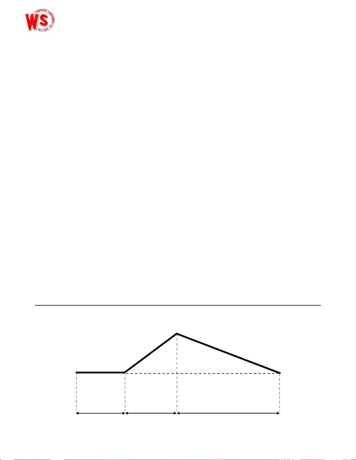
Typical Integrator Amplifier Output Waveform (INT Pin)
AUTO ZERO PHASE
(COUNTS)
2999 - 1000
SIGNAL INTEGRATE
PHASE FIXED
1000 COUNTS
TOTAL CONVERSION TIME = 4000 x t
DE-INTEGRATE PHASE
0 - 1999 COUNTS
= 16,000 x t
CLOCK
OSC
Page 5
Detailed Description
WS7106 / WS7107
WS7106 and
WS
WS7106 AND WS7107
5
Analog Section
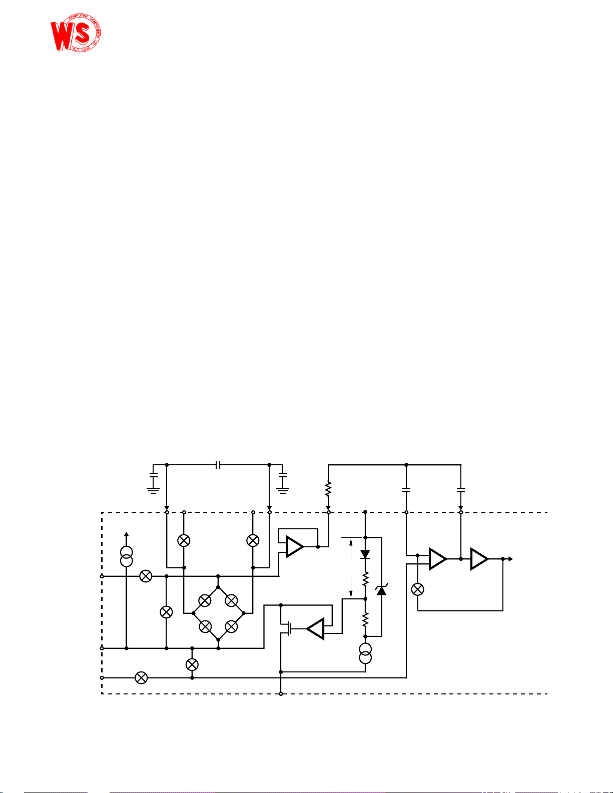
Figure3showstheAnalogSectionforthe
7107.Eachmeasurementcycleisdividedintothree
phases. They are (1) auto-zero (A-Z), (2) signal integrate
(INT) and (3) de-integrate (DE).
Auto-Zer o Phase
During auto-zero three things happen. First, input high and
low are disconnected from the pins and internally shorted to
analog COMMON. Second, the reference capacitor is
charged to the reference voltage. Third, a feedback loop is
closed around the system to charge the auto-zero capacitor
C
to compensate for offset voltages in the buffer amplifier,
AZ
integrator,and comparator. Since the comparator is included
in the loop, the A-Z accuracy is limited only by the noise of
the system. In any case, the offset referred to the input is
less than 10µV.
Signal Integrate Phase
During signal integrate, the auto-zero loop is opened, the
internal short is removed, and the internal input high and low
are connected to the external pins. The converter then
integrates the differential voltage between IN HI and IN LO
for a fixed time. This differential voltage can be within a wide
common mode range: up to 1V from either supply. If, on the
other hand, the input signal has no return with respect to the
converter power supply, IN LO can be tied to analog
COMMON to establish the correct common mode voltage. At
the end of this phase, the polarity of the integrated signal is
determined.
De-Integrate Phase
The final phase is de-integrate, or reference integrate. Input
low is internally connected to analog COMMON and input
high is connected across the previously charged reference
capacitor. Circuitry within the chip ensures that the capacitor
will be connected with the correct polarity to cause the
integrator output to return to zero. The time required for the
output to return to zero is proportional to the input signal.
Specifically the digital reading displayed is:
V
IN
---------------
DISPLAY COUNT = 1000
.
V
REF
Differential Input
The input can accept differential voltages anywhere within the
common mode range of the input amplifier,or specifically from
0.5V below the positive supply to 1V above the negative supply. In this range, the system has a CMRR of 86dB typical.
Howev er, care must be exercised to assure the integrator output does not saturate. A worst case condition would be a large
positive common mode voltage with a near full scale negative
differential input voltage. The negative input signal drives the
integrator positive when most of its swing has been used up
by the positive common mode voltage. For these critical applications the integrator output swing can be reduced to less
than the recommended 2V full scale swing with little loss of
accuracy. The integrator output can swing to within 0.3V of
either supply without loss of linearity.
IN HI
COMMON
IN LO
STRAY STRAY
REF HI
+
C
REF
V+
31
32
30
34
10µA
INT
A-Z
INT
C
REF
REF LO
36
A-Z A-Z
DE- DE+
A-Z AND DE(±)
FIGURE 3.ANALOG SECTION OF
35
DE-DE+
R
INT
-
C
REF
33
-
+
INPUT
HIGH
N
V-
BUFFER
28 29 27
-
+
V+
1
2.8V
C
AZ
A-Z INT
INTEGRATOR
6.2V
INPUT
LOW
A-Z
-
+
COMPARATOR
C
INT
-
+
TO
DIGITAL
SECTION
Page 6
Differential Reference
WS7106 / WS7107
(WS7106) or for any system
WS7107, the internal heating
The WS
WS7106
WS7106
WS7107
WS7106
WS7107
WS7106 it is
6
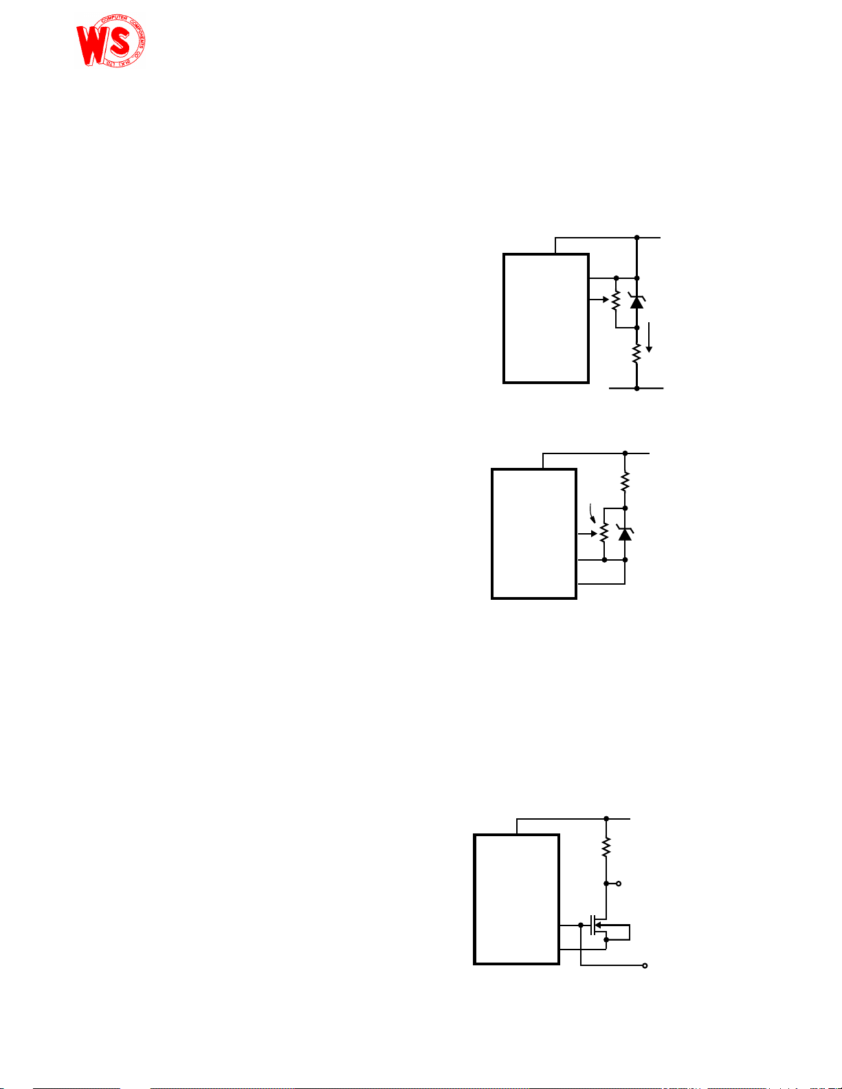
The reference voltage can be generated anywhere within the
powersupply voltage of the converter.The main source of common mode error is a roll-over voltage caused by the reference
capacitor losing or gaining charge to stray capacity on its
nodes. If there is a large common mode voltage, the reference
capacitor can gain charge (increase voltage) when called up to
de-integrate a positive signal but lose charge (decrease voltage) when called up to de-integrate a negative input signal.
This difference in reference for positive or negative input voltage
will give a roll-over error. However, by selecting the reference
capacitor such that it is large enough in comparison to the stray
capacitance, this error can be held to less than 0.5 count worst
case. (See Component V alue Selection.)
Analog COMMON
This pin is included primarily to set the common mode
voltageforbatteryoperation
where the input signals are floating with respect to the power
supply. The COMMON pin sets a voltage that is approximately 2.8V more negative than the positive supply. This is
selected to give a minimum end-of-life battery voltage of
about 6V. However, analog COMMON has some of the
attributes of a reference voltage. When the total supply
voltage is large enough to cause the zener to regulate (>7V),
the COMMON voltage will have a low voltage coefficient
(0.001%/V), low output impedance (≅15Ω), and a
temperature coefficient typically less than 80ppm/
o
C.
should be since this removes the common mode voltage
from the reference system.
Within the lC, analog COMMON is tied to an N-Channel FET
that can sink approximately 30mA of current to hold the
voltage 2.8V below the positive supply (when a load is trying
to pull the common line positive). However, there is only
10µA of source current, so COMMON mayeasily be tied to a
more negative voltage thus overriding the internal reference.
V+
V
REF HI
V+
V-
6.8kΩ
6.8V
ZENER
I
Z
REF LO
FIGURE 4A.
V
20kΩ
The limitations of the on chip reference should also be
recognized,however.Withthe
which results from the LED drivers can cause some
degradation in performance. Due to their higher thermal resistance, plastic parts are poorer in this respect than ceramic.
The combination of reference Temperature Coefficient (TC),
internal chip dissipation, and package thermal resistance can
increase noise near full scale from 25µVto80µV
. Also the
P-P
linearity in going from a high dissipation count such as 1000
(20 segments on) to a low dissipation count such as 1111(8
segments on) can suffer by a count or more. Devices with a
positive TC referencemay require several counts to pull out of
an over-range condition. This is because over-range is a low
dissipation mode, with the three least significant digits
blanked. Similarly, units with a negative TC may cycle
between over-range and a non-over-range count as the die
alternately heats and cools. All these problems are of course
eliminated if an external reference is used.
7106,withitsnegligibledissipation,suffersfrom
none of these problems. In either case, an external
reference can easily be added, as shown in Figure 4.
Analog COMMON is also used as the input low return during
auto-zero and de-integrate. If IN LO is different from analog
COMMON, a common mode voltage exists in the system
and is taken care of by the excellent CMRR of the converter.
However, in some applications IN LO will be set at a fixed
known voltage (power supply common for instance). In this
application, analog COMMON should be tied to the same
point, thus removing the common mode voltage from the
converter. The same holds true for the reference voltage. If
reference can be conveniently tied to analog COMMON, it
REF HI
REF LO
COMMON
FIGURE 4B.
FIGURE 4. USING AN EXTERNAL REFERENCE
ICL8069
1.2V
REFERENCE
TEST
TheTESTpinservestwofunctions.Onthe
coupled to the internally generated digital supply through a
500Ω resistor. Thus it can be used as the negative supply for
externally generated segment drivers such as decimal points
or any other presentation the user may want to include on
the LCD display. Figures 5 and 6 show such an application.
No more than a 1mA load should be applied.
V+
BP
21
TEST
37
FIGURE 5. SIMPLE INVERTER FOR FIXED DECIMAL POINT
1MΩ
TO LCD
DECIMAL
POINT
TO LCD
BACKPLANE
Page 7
The second function is a “lamp test”. When TEST is pulled
WS7106 / WS7107
WS7106
FIGURE 7. WS
WS7106 and
WS7107, respectively. In the WS7106
WS7107. It is identical
to the WS
7
high (to V+) all segments will be turned on and the display
should read “1888”. The TEST pin will sink about 15mA
under these conditions.
CAUTION: In the lamp test mode, the segments have a constant DC
voltage (no square-wave). This may burn the LCD display if maintained for extended periods.
CD4030
GND
V+
TO LCD
DECIMAL
POINTS
V+
TEST
BP
DECIMAL
POINT
SELECT
Digital Section
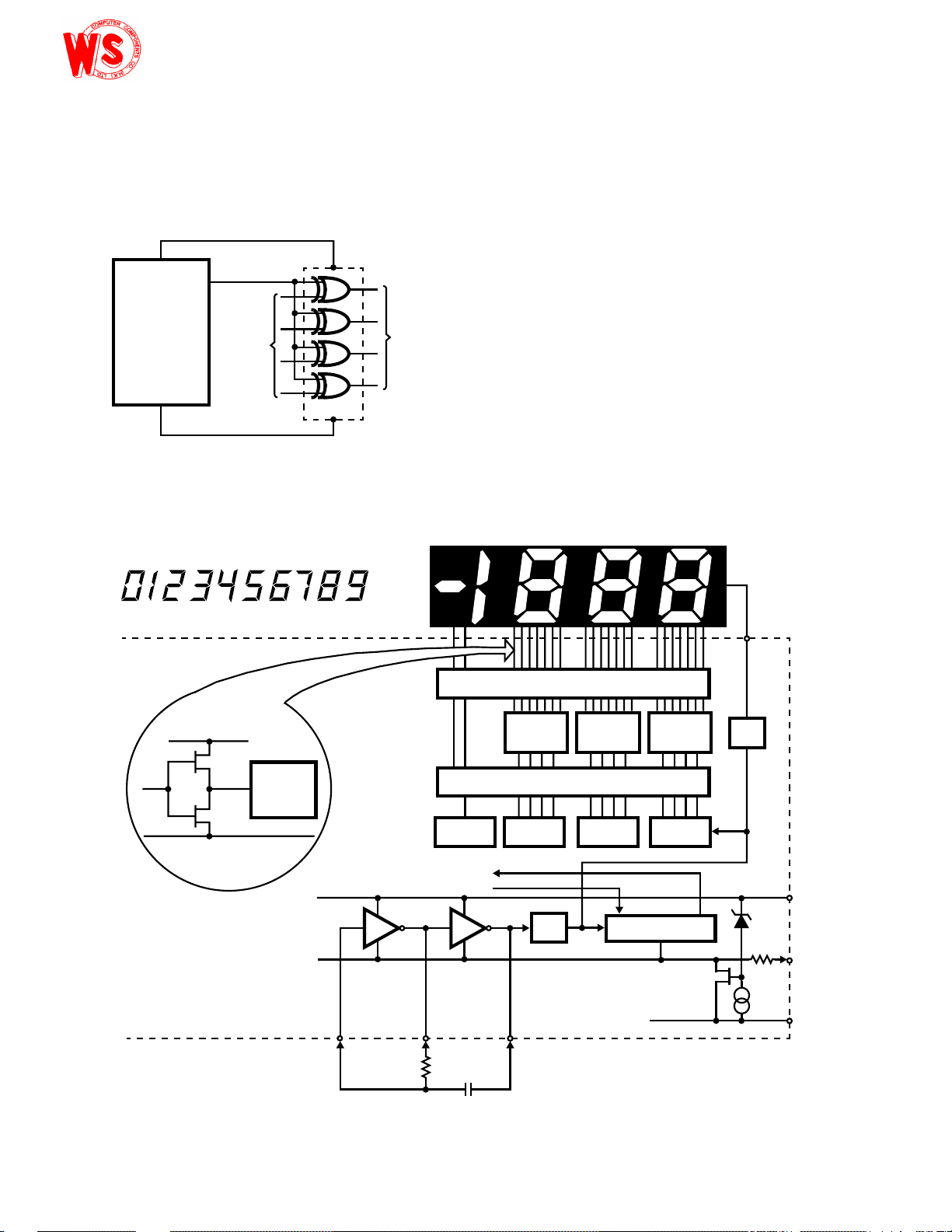
Figures7and8showthedigitalsectionforthe
,aninternaldigital
ground is generated from a 6V Zener diode and a large
P-Channel source follower. This supply is made stiff to
absorb the relative large capacitive currents when the back
plane (BP) voltage is switched. The BP frequency is the
clock frequency divided by 800. For three readings/sec., this
is a 60Hz square wave with a nominal amplitude of 5V. The
segments are driven at the same frequency and amplitude
and are in phase with BP when OFF, but out of phase when
ON. In all cases negligible DC voltage exists across the
segments.
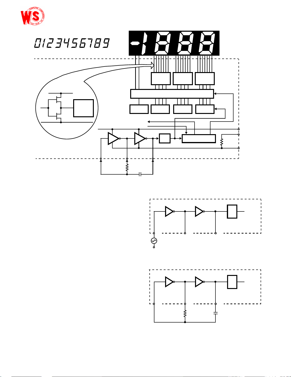
Figure8istheDigitalSectionofthe
7106exceptthattheregulatedsupplyandback
plane drive have been eliminated and the segment drive has
been increased from 2mA to 8mA, typical for instrument size
common anode LED displays. Since the 1000 output (pin 19)
must sink current from two LED segments, it has twice the
drive capability or 16mA.
FIGURE 6. EXCLUSIVE ‘OR’ GATE FOR DECIMAL POINT DRIVE
TYPICAL SEGMENT OUTPUT
INTERNAL DIGITAL GROUND
0.5mA
2mA
V+
SEGMENT
OUTPUT
1000’s 100’s 10’s 1’s
COUNTER
TO SWITCH DRIVERS
FROM COMPARATOR OUTPUT
CLOCK
†
† THREE INVERTERS
ONE INVERTER SHOWN FOR CLARITY
40 39 38
In both devices, the polarity indication is “on” for negative
analog inputs. If IN LO and IN HI are reversed,this indication
can be reversed also, if desired.
a
f
a
b
g
e
b
c
d
LCD PHASE DRIVER
7
SEGMENT
DECODE
LATCH
COUNTER COUNTER COUNTER
÷4
INTERNAL
DIGITAL
GROUND
f
c
e
SEGMENT
DECODE
7
a
g
c
d
LOGIC CONTROL
b
a
f
g
e
d
7
SEGMENT
DECODE
VTH = 1V
b
c
BACKPLANE
21
÷200
1
V+
6.2V
500Ω
TEST
37
26
V-
OSC 1
OSC 2
OSC 3
7106 DIGITAL SECTION
Page 8
a
WS7106 / WS7107
FIGURE 8. WS
WS7107
WS7106
WS7106 and WS7107
8
f
a
b
g
e
b
c
d
a
f
b
g
c
e
c
d
a
f
b
g
e
c
d
TYPICAL SEGMENT OUTPUT
DIGITAL GROUND
0.5mA
8mA
V+
TO
SEGMENT
1000’s 100’s 10’s 1’s
COUNTER
FROM COMPARATOR OUTPUT
TO SWITCH DRIVERS
V+
CLOCK
†
† THREE INVERTERS
ONE INVERTER SHOWN FOR CLARITY
System Timing
Figure9showstheclockingarrangementusedinthe
.Twobasicclockingarrangements
can be used:
40 39 38
OSC 1
OSC 2
7
SEGMENT
DECODE
LATCH
COUNTER COUNTER COUNTER
÷4
OSC 3
7
SEGMENT
DECODE
LOGIC CONTROL
7107 DIGITAL SECTION
INTERNAL TO PART
7
SEGMENT
DECODE
500Ω
÷4
1
37
27
V+
TEST
DIGITAL
GROUND
CLOCK
1. Figure 9A. An external oscillator connected to pin 40.
2. Figure 9B. An R-C oscillator using all three pins.
The oscillator frequency is divided by four before it clocks the
decade counters. It is then further divided to form the three
convert-cycle phases. These are signal integrate (1000
counts), reference de-integrate (0 to 2000 counts) and
auto-zero (1000 to 3000 counts). For signals less than full
scale, auto-zero gets the unused portion of reference
de-integrate. This makes a complete measure cycle of 4,000
counts (16,000 clock pulses) independent of input voltage.
For three readings/second, an oscillator frequency of 48kHz
would be used.
To achieve maximum rejection of 60Hz pickup, the signal
integrate cycle should be a multiple of 60Hz. Oscillator
frequencies of 240kHz, 120kHz, 80kHz, 60kHz, 48kHz,
40kHz, 33
tion, Oscillator frequencies of 200kHz, 100kHz, 66
1
/3kHz, etc. should be selected. For 50Hz rejec-
2
/3kHz,
50kHz, 40kHz, etc. would be suitable. Note that 40kHz (2.5
readings/second) will reject both 50Hz and 60Hz (also
400Hz and 440Hz).
40 39
GND
TEST
INTERNAL TO PART
40 39
FIGURE 9. CLOCK CIRCUITS
FIGURE 9A.
R
FIGURE 9B.
38
÷4
38
C
RC OSCILLATOR
CLOCK
Page 9
Component Value Selection
WS7106 / WS7107
WS7106 or the WS7107, When the
WS7107 with +5V
The WS
network on the input. The WS
WS7107 Power Supplies
WS7107
9
Integrating Resistor
Both the buffer amplifier and the integrator have a class A
output stage with 100µA of quiescent current. They can
supply 4µA of drive current with negligible nonlinearity. The
integrating resistor should be large enough to remain in this
very linear region over the input voltage range, but small
enough that undue leakage requirements are not placed on
the PC board. For 2V full scale, 470kΩ is near optimum and
similarly a 47kΩ for a 200mV scale.
Integrating Capacitor
The integrating capacitor should be selected to give the
maximum voltage swing that ensures tolerance buildup will
not saturate the integrator swing (approximately. 0.3V from
eithersupply).Inthe
analog COMMON is used as a reference, a nominal +2V fullscaleintegratorswingisfine.Forthe
supplies and analog COMMON tied to supply ground, a
±3.5V to +4V swing is nominal. For three readings/second
(48kHz clock) nominal values for C
0.10µF, respectively. Of course, if different oscillator frequencies are used, these values should be changed in inverse
proportion to maintain the same output swing.
An additional requirement of the integrating capacitor is that
it must have a low dielectric absorption to prevent roll-over
errors. While other types of capacitors are adequate for this
application, polypropylene capacitors give undetectable
errors at reasonable cost.
Auto-Zero Capacitor
The size of the auto-zero capacitor has some influence on
the noise of the system. For 200mV full scale where noise is
very important, a 0.47µF capacitor is recommended. On the
2V scale, a 0.047µF capacitor increases the speed of recovery from overload and is adequate for noise on this scale.
are 0.22µF and
lNT
Reference Voltage
The analog input required to generate full scale output (2000
counts) is: V
V
should equal 100mV and 1V, respectively. However, in
REF
lN
=2V
. Thus, for the 200mV and 2V scale,
REF
many applications where the A/D is connected to a
transducer, there will exist a scale factor other than unity
between the input voltage and the digital reading. For
instance, in a weighing system, the designer might like to
have a full scale reading when the voltage from the
transducer is 0.662V. Instead of dividing the input down to
200mV, the designer should use the input voltage directly
and select V
= 0.341V. Suitable values for integrating
REF
resistor and capacitor would be 1 20kΩ and 0.22µF. This
makes the system slightly quieter and also avoids a divider
7107with±5Vsuppliescan
accept input signals up to ±4V. Another advantage of this
system occurs when a digital reading of zero is desired for
V
≠ 0. Temperature and weighing systems with a variable
IN
fare are examples. This offset reading can be conveniently
generated by connecting the voltage transducer between IN
HI and COMMON and the variable (or fixed) offset voltage
between COMMON and IN LO.
7107isdesignedtoworkfrom±5Vsupplies.
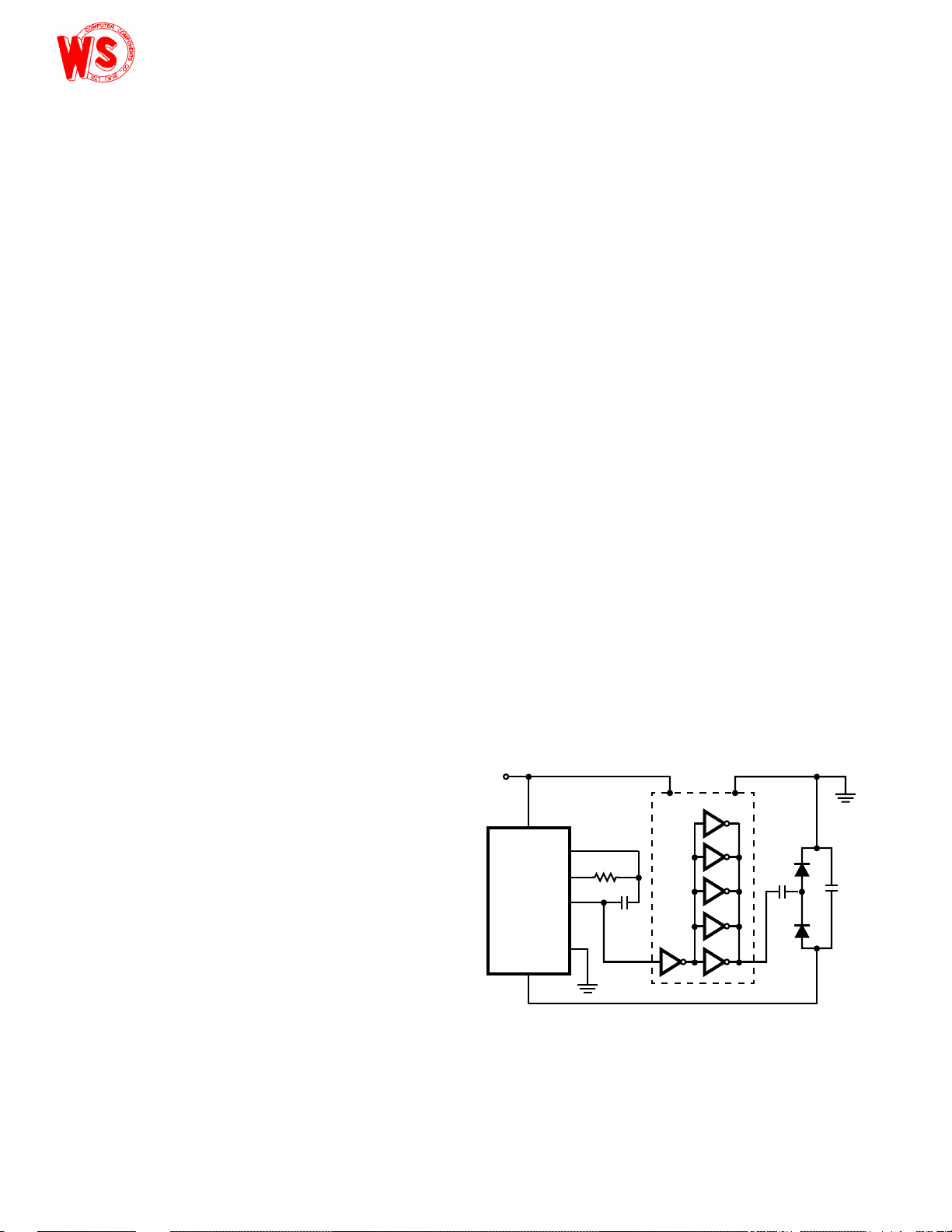
However, if a negative supply is not available, it can be
generated from the clock output with 2 diodes, 2 capacitors,
and an inexpensivelC.Figure 10 shows this application. See
ICL7660 data sheet for an alternative.
In fact, in selected applications no negative supply is
required. The conditions to use a single +5V supply are:
1. The input signal can be referenced to the center of the
common mode range of the converter.
2. The signal is less than ±1.5V.
3. An external reference is used.
Reference Capacitor
A 0.1µF capacitor gives good results in most applications.
However, where a large common mode voltage exists (i.e.,
the REF LO pin is not at analog COMMON) and a 200mV
scale is used, a larger value is required to prevent roll-over
error. Generally 1µF will hold the roll-over error to 0.5 count
in this instance.
Oscillator Components
For all ranges of frequency a 100kΩ resistor is recommended
and the capacitor is selected from the equation:
0.45
-----------
RC
For 48kHz Clock (3 Readings/sec),=
f
C 100pF.=
V+
CD4009
V+
OSC 1
OSC 2
OSC 3
GND
V-
V- = 3.3V
FIGURE 10. GENERATING NEGATIVE SUPPLY FROM +5V
IN914
0.047
µF
IN914
+
10
µF
-
Page 10
Typical Applications
WS7106 / WS7107
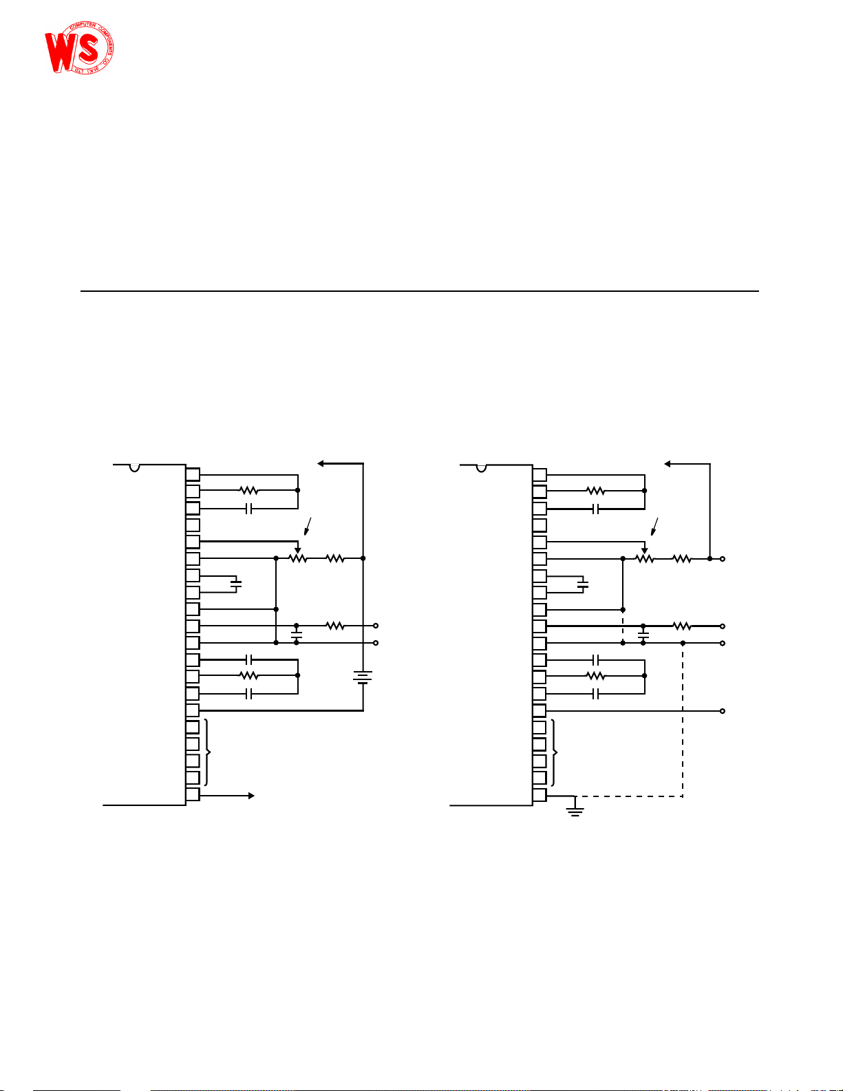
The WS7106 and WS7107 may be used in a wide variety of configurations. The
circuits which follow show some of the possibilities, and serve to illustrate the
exceptional versatility of these A/D converters.
FIGURE 11 WS7106 USING THE INTERNAL REFERENCE
FIGURE 12. WS7107 USING THE INTERNAL REFERENCE
10
TYPICAL APPLICATIONS
OSC 1
OSC 2
OSC 3
TEST
REF HI
REF LO
C
REF
C
REF
COMMON
IN HI
IN LO
A-Z
BUFF
INT
V G2
C3
A3
G3
BP
40
39
38
37
36
35
34
33
32
31
30
29
28
27
26
25
24
23
22
21
TO DISPLAY
100kΩ
100pF
0.1µF
0.47µF
47kΩ
0.22µF
TO BACKPLANE
TO PIN 1
1kΩ 22kΩ
0.01µF
SET V
REF
= 100mV
1MΩ
+
IN
-
+
9V
-
Values shown are for 200mV full scale, 3 readings/sec., floating
supply voltage (9V battery).
OSC 1
OSC 2
OSC 3
TEST
REF HI
REF LO
C
REF
C
REF
COMMON
IN HI
IN LO
A-Z
BUFF
INT
V -
G2
C3
A3
G3
GND
40
39
38
37
36
35
34
33
32
31
30
29
28
27
26
25
24
23
22
21
TO DISPLAY
100kΩ
100pF
0.1µF
0.47µF
0.22µF
47kΩ
TO PIN 1
1kΩ 22kΩ
0.01µF
SET V
REF
= 100mV
1MΩ
+5V
+
IN
-
-5V
Values shown are for 200mV full scale, 3 readings/sec. IN LO may
be tied to either COMMON for inputs floating with respect to
supplies, or GND for single ended inputs. (See discussion under
Analog COMMON.)
Page 11
Typical Applications
t
r
WS7106 / WS7107
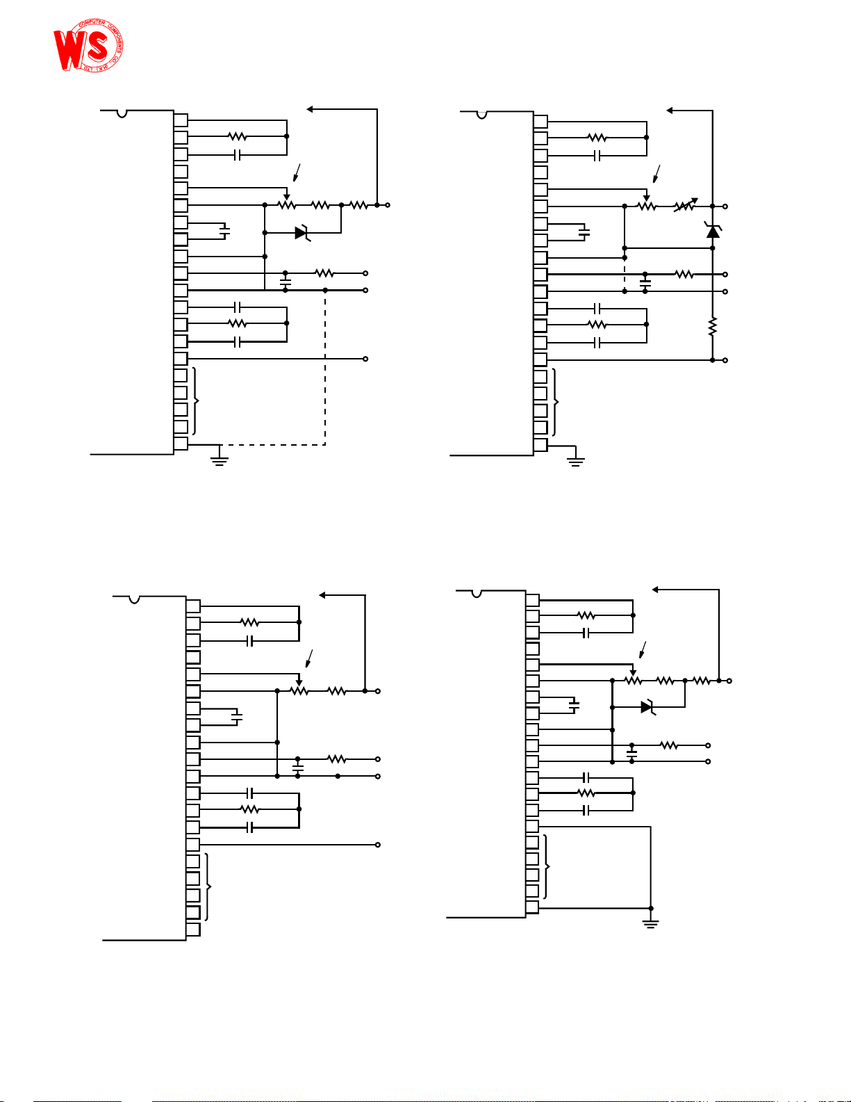
FIGURE 14. WS
FIGURE 13. WS
FIGURE 15. WS7106 AND WS7107; RECOMMENDED
FIGURE 16. WS
11
OSC 1
OSC 2
OSC 3
TEST
REF HI
REF LO
C
REF
C
REF
COMMON
IN HI
IN LO
A-Z
BUFF
INT
VG2
C3
A3
G3
GND
40
39
38
37
36
35
34
33
32
31
30
29
28
27
26
25
24
23
22
21
100kΩ
100pF
0.1µF
0.47µF
0.22µF
TO DISPLAY
(Continued)
TO PIN 1
1kΩ 10kΩ
47kΩ
SET V
= 100mV
1.2V (ICL8069)
1MΩ
0.01µF
REF
10kΩ
OSC 1
40
OSC 2
39
OSC 3
38
TEST
37
REF HI
36
V+
+
IN
-
-
V
REF LO
C
REF
C
REF
COMMON
IN HI
IN LO
A-Z
BUFF
INT
V -
G2
C3
A3
G3
GND
35
34
33
32
31
30
29
28
27
26
25
24
23
22
21
TO DISPLAY
100kΩ
100pF
0.1µF
0.47µF
0.22µF
47kΩ
TO PIN 1
1kΩ 100kΩ
0.01µF
SET V
REF
= 100mV
1MΩ
+5V
6.8V
+
IN
-
-5V
IN LO is tied to supply COMMON establishing the correct common mode
voltage. If COMMON is not shorted to GND, the input voltage may floa
with respect to the power supply and COMMON acts as a pre-regulato
for the reference. If COMMON is shorted to GND, the input is single
ended (referred to supply GND) and the pre-regulator is overridden.
7107 WITH AN EXTERNAL BAND-GAP
REFERENCE (1.2V TYPE)
OSC 1
OSC 2
OSC 3
TEST
REF HI
REF LO
C
REF
C
REF
COMMON
IN HI
IN LO
A-Z
BUFF
INT
V G2
C3
A3
G3
BP/GND
40
39
38
37
36
35
34
33
32
31
30
29
28
27
26
25
24
23
22
21
TO DISPLAY
100kΩ
100pF
0.1µF
0.047µF
470kΩ
0.22µF
TO PIN 1
25kΩ 24kΩ
0.01µF
SET V
REF
= 100mV
1MΩ
V+
+
IN
-
V-
Since low TC zeners have breakdown voltages ~ 6.8V, diode must
be placed across the total supply (10V). As in the case of Figure 14,
IN LO may be tied to either COMMON or GND.
7107 WITH ZENER DIODE REFERENCE
OSC 1
OSC 2
OSC 3
TEST
REF HI
REF LO
C
REF
C
REF
COMMON
IN HI
IN LO
A-Z
BUFF
INT
V G2
C3
A3
G3
GND
40
39
38
37
36
35
34
33
32
31
30
29
28
27
26
25
24
23
22
21
TO DISPLAY
100kΩ
100pF
0.1µF
0.47µF
0.22µF
47kΩ
TO PIN 1
1kΩ 10kΩ
SET V
= 100mV
1.2V (ICL8069)
1MΩ
0.01µF
REF
15kΩ
+5V
+
IN
-
An external reference must be used in this application, since the
voltage between V+ and V- is insufficient for correct operation of the
internal reference.
COMPONENT VALUES FOR 2V FULL SCALE
7107 OPERATED FROM SINGLE +5V
Page 12
Typical Applications
WS7106 / WS7107
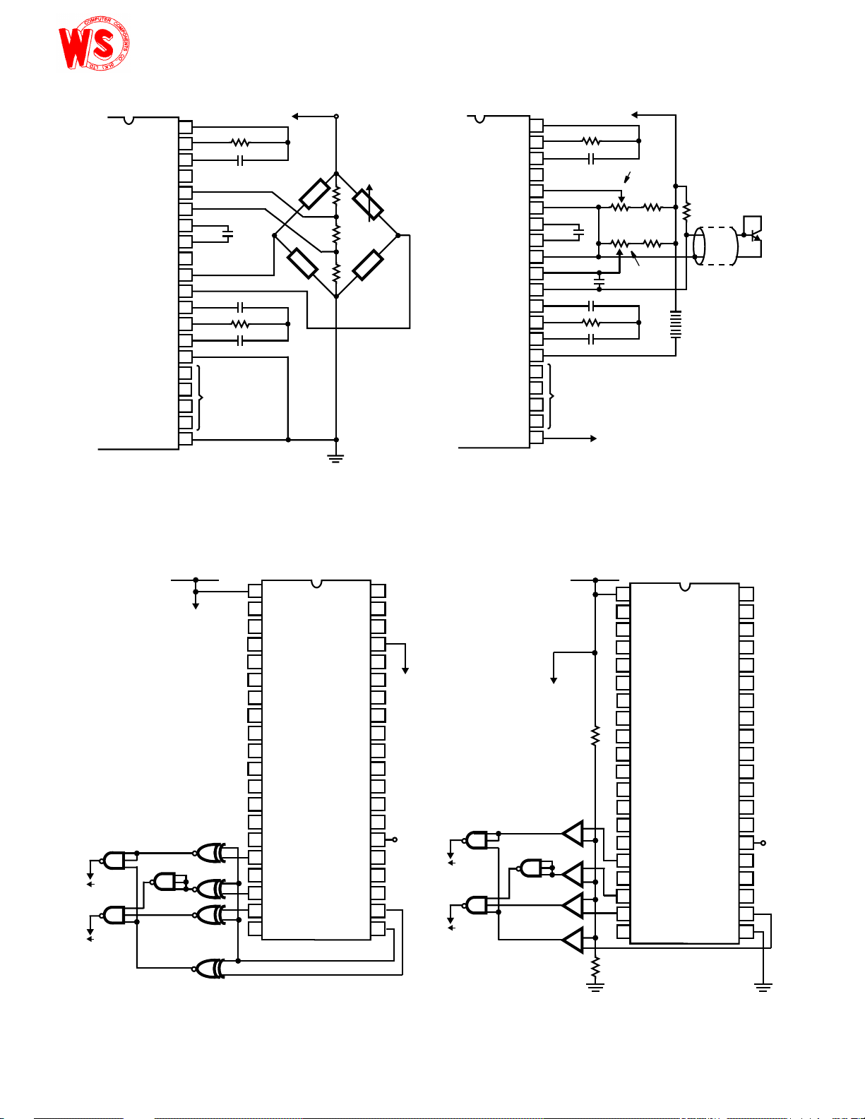
FIGURE 18. WS
FIGURE 17. WS
12
WS7106 OUTPUTS
WS7107 OUTPUT
40
OSC 1
39
OSC 2
38
OSC 3
37
TEST
36
REF HI
C
REF
C
REF
IN HI
IN LO
A-Z
BUFF
INT
V G2
C3
A3
G3
GND
35
34
33
32
31
30
29
28
27
26
25
24
23
22
21
TO DISPLAY
REF LO
COMMON
(Continued)
TO PIN 1
100kΩ
100pF
0.1µF
0.47µF
47kΩ
0.22µF
V+
The resistor values within the bridge are determined by the desired
sensitivity.
7107MEASUREINGRATIOMETRICVALUESOF
QUAD LOAD CELL
V+
OSC 1
OSC 2
OSC 3
TEST
REF HI
C
REF
C
REF
IN HI
IN LO
A-Z
BUFF
INT
G2
C3
A3
G3
BP
40
39
38
37
36
35
TO
LOGIC
34
GND
33
32
31
30
29
28
27
26
V-
V25
24
23
22
21
O /RANGE
U /RANGE
CD4023 OR
74C10
TO LOGIC
V
CC
CD4077
1
V+
D1
2
C1
3
B1
4
A1
5
F1
6
G1
7
E1
8
D2
9
C2
10
B2
11
A2
12
F2
13
E2
14
D3
15
B3
16
F3
17
E3
18
AB4
19
POL
20
REF LO
COMMON
FIGURE 19. CIRCUIT FOR DEVELOPING UNDERRANGE AND
OVERRANGE SIGNAL FROM
OSC 1
OSC 2
OSC 3
TEST
REF HI
REF LO
C
REF
C
REF
COMMON
IN HI
IN LO
A-Z
BUFF
INT
V -
G2
C3
A3
G3
BP
40
39
38
37
36
35
34
0.1µF
33
32
31
30
29
28
27
26
25
24
23
22
21
TO PIN 1
100kΩ
100pF
0.01µF
47kΩ
0.22µF
TO DISPLAY
SCALE
FACTOR
ADJUST
100kΩ 1MΩ
100kΩ 220kΩ
ZERO
ADJUST
0.47µF
TO BACKPLANE
22kΩ
SILICON NPN
MPS 3704 OR
SIMILAR
9V
A silicon diode-connected transistor has a temperature coefficient of
about -2mV/oC. Calibration is achieved by placing the sensing
transistor in ice water and adjusting the zeroing potentiometer for a
000.0 reading. The sensor should then be placed in boiling water
and the scale-factor potentiometer adjusted for a 100.0 reading.
7106 USED AS A DIGITAL CENTIGRADE
THERMOMETER
+5V
OSC 1
OSC 2
OSC 3
TEST
REF HI
C
REF
C
REF
IN HI
IN LO
A-Z
BUFF
INT
G2
C3
A3
G3
BP
40
39
38
37
36
35
34
33
32
31
30
29
28
27
26
V-
V25
24
23
22
21
TO LOGIC
V
CC
12kΩ
The LM339 is required to
ensure logic compatibility
with heavy display loading.
O /RANGE
U /RANGE
CD4023 OR
74C10
1
V+
D1
2
C1
3
B1
4
A1
5
F1
6
G1
7
E1
8
D2
9
C2
10
B2
11
A2
12
F2
13
E2
+
-
+
-
+
-
-
+
14
15
16
17
18
19
20
33kΩ
D3
B3
F3
E3
AB4
POL
REF LO
COMMON
FIGURE 20. CIRCUIT FOR DEVELOPING UNDERRANGE AND
OVERRANGE SIGNALS FROM
Page 13
Typical Applications
WS7106 / WS7107
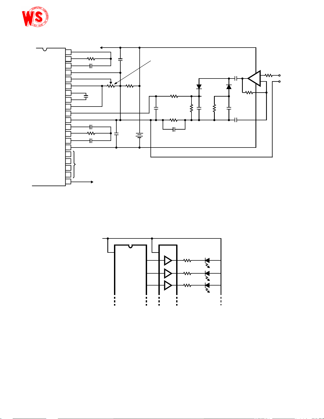
FIGURE 21. AC TO DC CONVERTER WITH WS7106
13
(Continued)
OSC 1
OSC 2
OSC 3
TEST
REF HI
REF LO
C
REF
C
REF
COMMON
IN HI
IN LO
A-Z
BUFF
INT
VG2
C3
A3
G3
BP
40
39
38
37
36
35
34
33
32
31
30
29
28
27
26
25
24
23
22
21
TO PIN 1
100kΩ
100pF
0.1µF
0.47µF
47kΩ
0.22µF
TO DISPLAY
1kΩ 22kΩ
10µF
TO BACKPLANE
10µF
SCALE FACTOR ADJUST
(V
= 100mV FOR AC TO RMS)
REF
470kΩ
1µF
4.3kΩ
+
9V
-
100pF
(FOR OPTIMUM BANDWIDTH)
10kΩ
1µF
1N914
10kΩ
Test is used as a common-mode reference level to ensure compatibility with most op amps.
5µF
1µF
0.22µF
CA3140
2.2MΩ
+
-
100kΩ
AC IN
+5V
LED
SEGMENTS
ICL7107
DM7407
130Ω
130Ω
130Ω
FIGURE 22. DISPLAY BUFFERING FOR INCREASED DRIVE CURRENT
Page 14
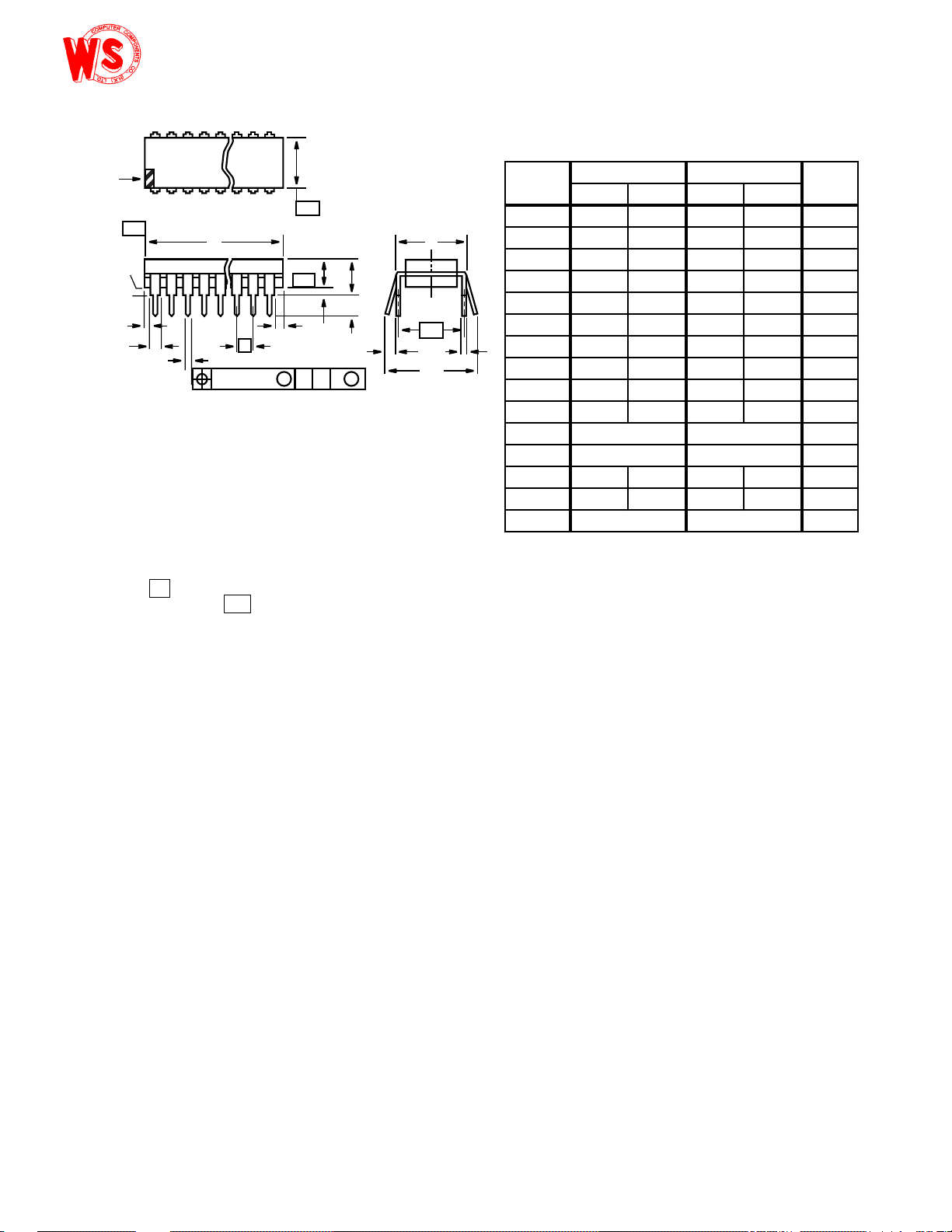
Dual-In-Line Plastic Packages (PDIP)
WS7106 / WS7107
14
N
D1
-C-
E1
-B-
A1
A2
E
A
L
e
C
S
C
L
e
A
e
INDEX
AREA
BASE
PLANE
SEATING
PLANE
D1
B1
1 2 3 N/2
-AD
e
B
0.010 (0.25) C AMB
NOTES:
1. Controlling Dimensions: INCH.In case ofconflictbetween English
and Metric dimensions, the inch dimensions control.
2. Dimensioning and tolerancing per ANSI Y14.5M-1982.
3. Symbols are definedinthe “MO Series SymbolList”in Section 2.2
of Publication No. 95.
4. Dimensions A, A1andL are measured withthepackage seated in
JEDEC seating plane gauge GS-3.
5. D, D1,and E1dimensionsdo notinclude moldflashor protrusions.
Mold flash or protrusions shall not exceed 0.010 inch (0.25mm).
6. E and are measured with the leads constrained to be per-
e
pendicular to datum .
A
-C-
7. eB and eC are measured at the lead tips with the leads unconstrained. eC must be zero or greater.
8. B1 maximum dimensions do not include dambar protrusions.
Dambar protrusions shall not exceed 0.010 inch (0.25mm).
9. N is the maximum number of terminal positions.
10. Corner leads (1, N, N/2 and N/2 + 1) for E8.3, E16.3,E18.3,E28.3,
E42.6 will haveaB1dimensionof0.030-0.045inch(0.76-1.14mm).
E40.6 (JEDEC MS-011-AC ISSUE B)
40 LEAD DUAL-IN-LINE PLASTIC PACKAGE
INCHES MILLIMETERS
SYMBOL
A - 0.250 - 6.35 4
A1 0.015 - 0.39 - 4
A2 0.125 0.195 3.18 4.95 -
B 0.014 0.022 0.356 0.558 B1 0.030 0.070 0.77 1.77 8
C 0.008 0.015 0.204 0.381 -
C
B
D 1.980 2.095 50.3 53.2 5
D1 0.005 - 0.13 - 5
E 0.600 0.625 15.24 15.87 6
E1 0.485 0.580 12.32 14.73 5
e 0.100 BSC 2.54 BSC e
A
e
B
0.600 BSC 15.24 BSC 6
- 0.700 - 17.78 7
L 0.115 0.200 2.93 5.08 4
N40 409
NOTESMIN MAX MIN MAX
 Loading...