

Page 1
SPEC NO: DSAE9422
REV NO: V.2 DATE:APR/19/2005 PAGE:
1OF4
APPROVED: J. Lu
CHECKED: Allen Liu DRAWN:
S.H.CHEN ERP: 1101007669
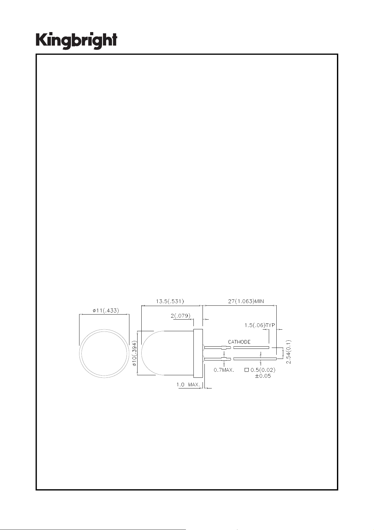
Package Dimen sion
s
Notes:
1. All dime nsions ar e in m illimete rs (inc hes)
.
2.
Tolerance i s
±0
.25(0.01") unless otherwise noted
.
3. Lead spaci ng is m easur ed wher e the l eads em erge from the p ackage.
4. Specificati ons are subj ect to change without notic e
.
10mm SOLID STATE LAMP
Description
The Yellow source color devices are made
with Gallium Arsenide Phosphide on Gallium
Phosphide Yellow Light Emitting Diode.
WP813YD YELLOW
Features
z
10mm DIAMETER BIG LAMP.
z
I.C. COMPATIBLE.
z
RELIABLE AND RUGGED.
z
LONG LIFE
-
SOLID STATE RELIABILITY
.zRoHS COMPLIANT.
Page 2
SPEC NO: DSAE9422
REV NO: V.2 DATE:APR/19/2005 PAGE:
2OF4
APPROVED: J. Lu
CHECKED: Allen Liu DRAWN:
S.H.CHEN ERP: 1101007669
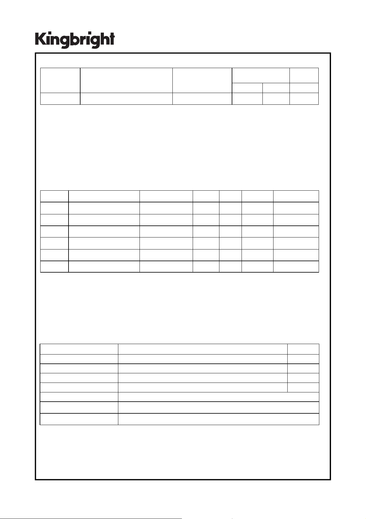
Electrical / Optical Characteristics at T
A
=25°CAbsolute Maximum Ratings at T
A
=25
°C
Notes:
1. 1/10 Duty Cycle, 0.1ms Pulse Width.
2. 2mm below package base.
3. 5mm below package bas e.
Selection Guid
e
Note:
1. θ1/2 is the angle from optical centerline where the luminous intensity is 1/2 the optical centerline value.
Symbol
Parameter
Device
Typ.
Max.
Test Conditions
Units
λ
peak
Peak Wavelength
Yellow
590nmIF=20mA
D
Dominant Wavelength
Yellow
588nmIF=20mA
1/2
Spectral Line Half
-
width
Yellow
35nmIF=20mA
C
Capacitance
Yellow
20pFVF=0V;f=1MHz
VFForward Voltage
Yellow
2.1
2.5VIF=20mA
IRReverse Current
Yellow
10uAVR= 5V
Parameter
Yellow
Units
Power dissipation
105mWDC Forward Current
30mAPeak Forward Current [1]
140mAReverse Voltage
5VOperating / Storage Temperature
-
40°C
To +85°C
Lead Solder Te mperature [2]
260°C
For 3 Seconds
Lead Solder Te mperature [3]
260°C
For 5 Seconds
Part No.
Dice
Lens Type
Iv (mcd)
@ 20mA
Viewing
Angle
Min.
Typ.
2 θ 1/2
WP813YD
YELLOW (GaAsP/GaP)
YELLOW
DIFFUSED
105060
°
∆λ
λ
Page 3
SPEC NO: DSAE9422
REV NO: V.2 DATE:APR/19/2005 PAGE:
3OF4
APPROVED: J. Lu
CHECKED: Allen Liu DRAWN:
S.H.CHEN ERP: 1101007669
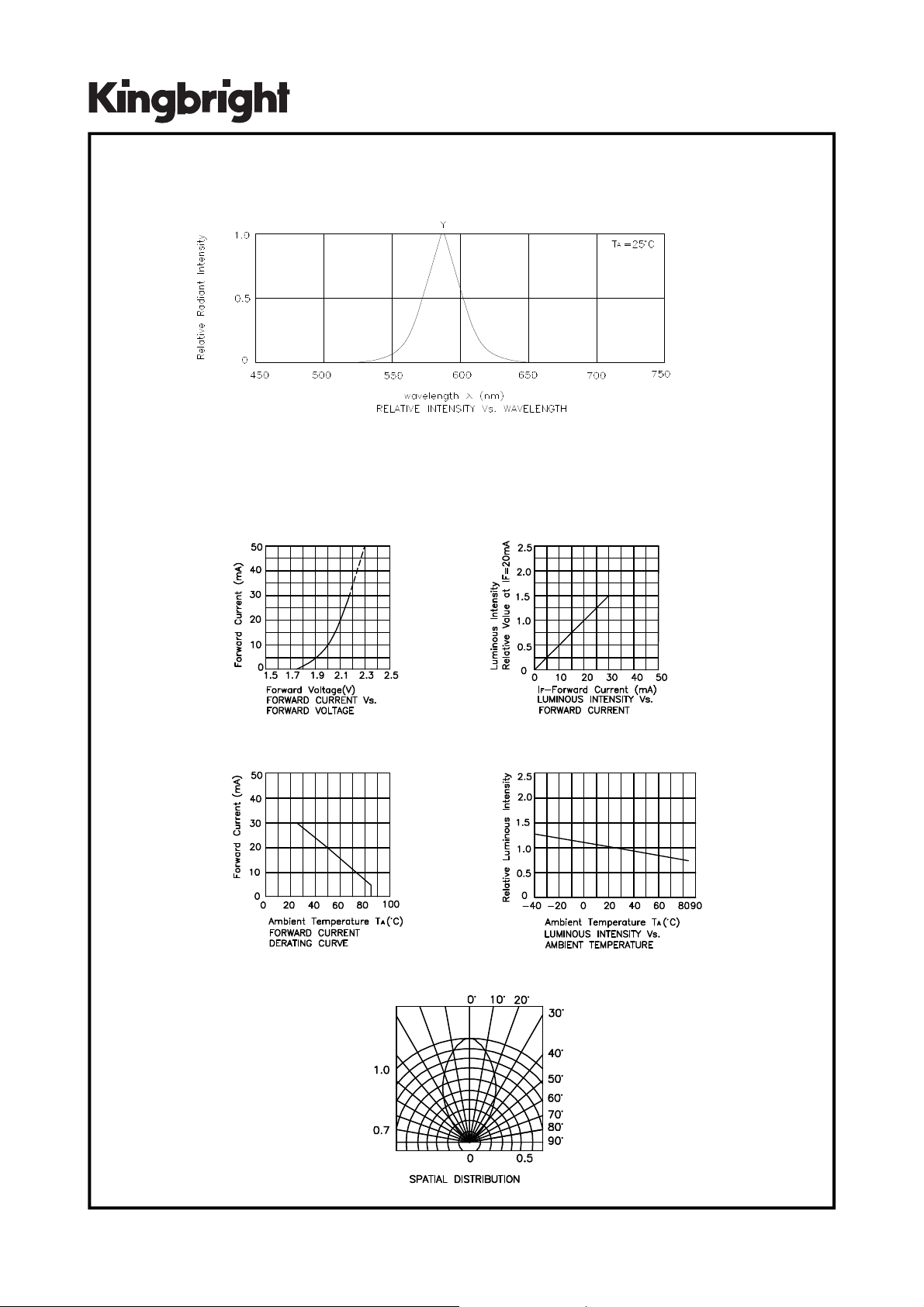
Yellow
WP813YD
Page 4
SPEC NO: DSAE9422
REV NO: V.2 DATE:APR/19/2005 PAGE:
4OF4
APPROVED: J. Lu
CHECKED: Allen Liu DRAWN:
S.H.CHEN ERP: 1101007669
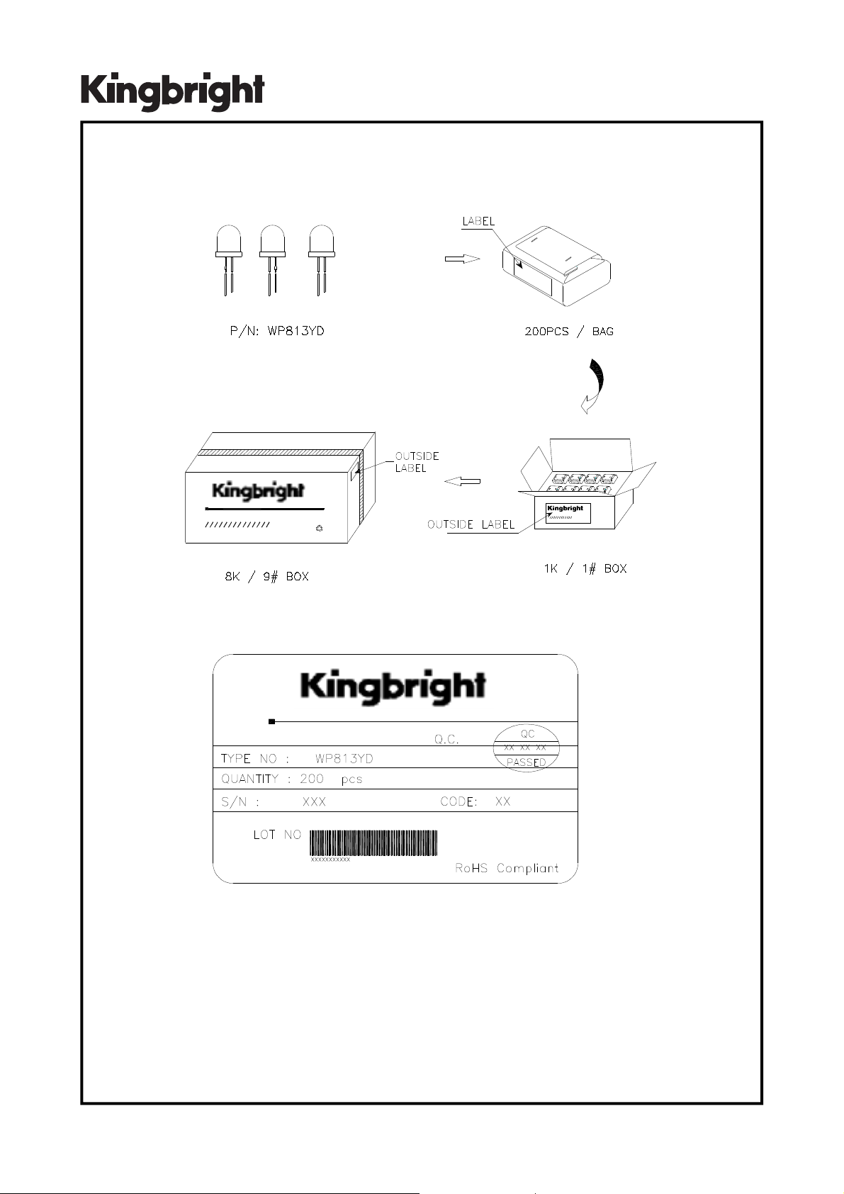
PACKING & LABEL SPECIFICATIONS WP813YD
Remarks:
If special sorting is required (e.g. binning based on forward voltage, luminous intensity, or wavelength),
the typical accuracy of the sorting process is as follows:
1. Wavelength: +/
-
1nm
2. Luminous Intensity: +/
-
15%
3. Forward Voltage: +/
-
0.1V
Note: Accuracy may depend on the sorting parameters.
 Loading...