

Page 1
查询WM8146供应商
WM8146
12-bit (8+4-bit) Linear Sensor Image Processor
Product Preview, January 2000 Rev 1.1
DESCRIPTION
The WM8146 is a 12-bit analogue front end/digitiser IC,
which processes and digitises t he analogue output signals
from linear CCD sensors at pixel sample rates of up to
6MSPS.
The device includes three analogue signal processing
channels each of which contains Reset Level Clamping,
Correlated Double Sampling and Program mable Gain and
Offset adjust functions. The output from each of these
channels is time m ultiplexed into a s ingle high-speed 12-bit
Analogue to Digital Converter. The digital output data is
available in 8+4-bit wide multiplexed form at, with no m iss ing
codes.
The WM8146 is controlled via a configurable serial
interface, which is compatible with all of Wolfson’s imaging
devices.
Powered from an analogue supply voltage of 5V and a
digital interface supply of either 5V or 3.3V, the W M8146
typically only consumes 175mW when operating from 5V
supplies.
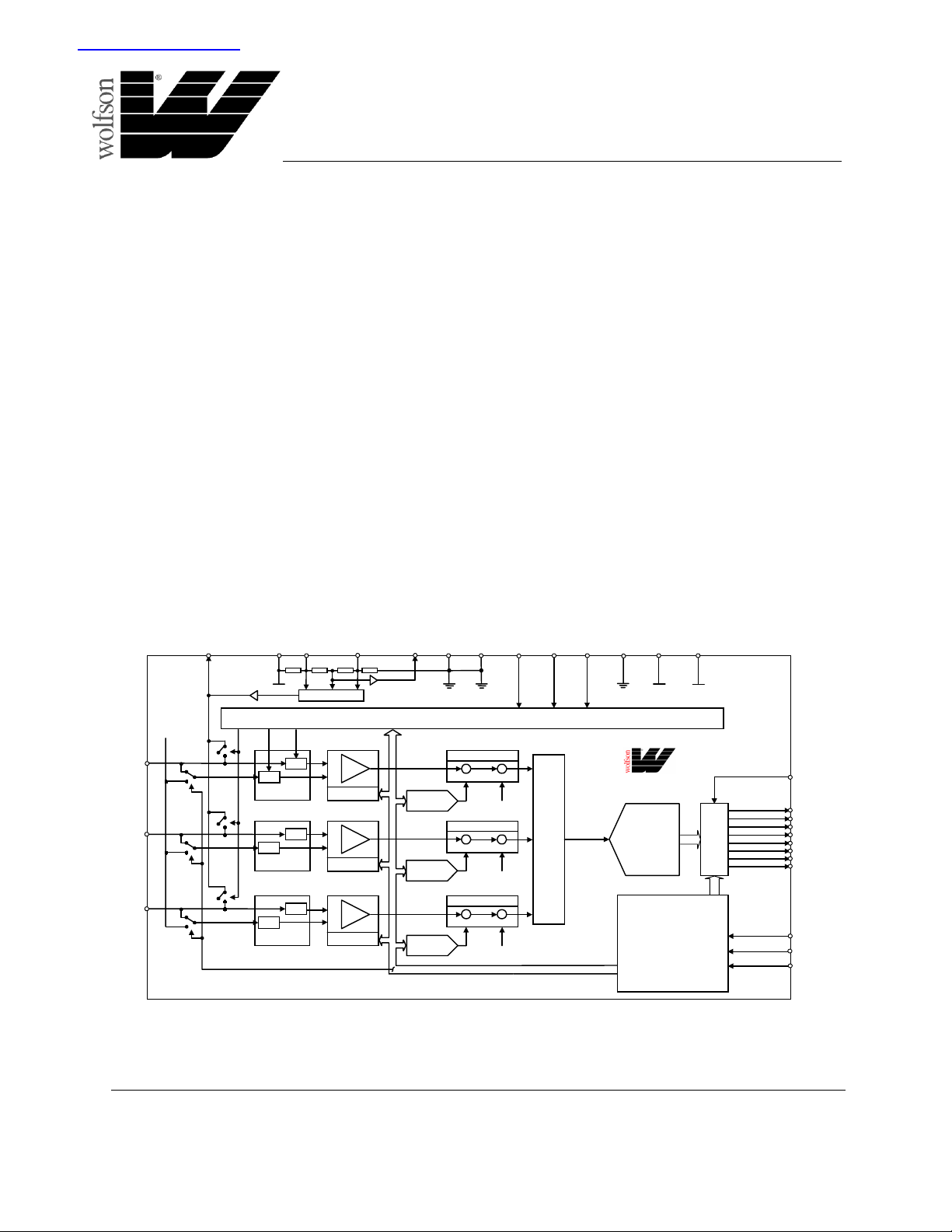
BLOCK DIAGRAM
VRLC
(26)
AVDD
(21)
VRT
(24)
VRB
(23)
VMID
(25)
AGND1
(22)
FEATURES
•
No missing codes guaranteed
•
6MSPS sample rate
•
Colour pixel by pixel or line by line sampling
•
Monochrome sampling
•
Selectable reset level clamp voltage
•
Pixel by pixel or line by line clamping
•
Correlated double sampling
•
5-bit programmable gain amplifier
•
8-bit + sign offset adjustment
•
5V or 3.3V digital interface compatibility
•
Serial control interface
•
28-pin SOIC package
APPLICATIONS
•
Flatbed scanners
•
Multi-function peripherals
•
Copier scanners
•
CCD sensor interfaces
AGND2
VSMP
MCLK
RLC
DGND
(2)
(5)
(7)
(6)
DVDD1
(8)
(3)
DVDD2
(10)
MUX
CL RS VS
S/H
S/H
CDS
S/H
S/H
CDS
S/H
S/H
CDS
PGA
5-BIT REG
PGA
5-BIT REG
PGA
5-BIT REG
8-BIT +
SIGN DAC
8-BIT +
SIGN DAC
8-BIT +
SIGN DAC
RINP
(1)
GINP(28)
BINP(27)
VMID
WOLFSON MICROELECTRONICS LTD
Lutton Court, Bernard Terrace, Edi nburgh, EH8 9NX, UK
Tel: +44 (0) 131 667 9386
Fax: +44 (0) 131 667 5176
Email: [email protected]
http://www.wolfson.co.uk
TIMING CONTROL
OFFSET
+ +
VMID
OFFSET
+ +
VMID
OFFSET
+ +
VMID
(4)
WM8146
M
U
X
12-bit
ADC
CONFIGURABLE
SERIAL CONTROL
INTERFACE
Product Preview
8+
4
M
U
X
data sheets contain
OEB
(13) OP[0]
(14)
OP[1]
(15)
OP[2]
OP[3]
(16)
(17)
OP[4]
(18)
OP[5]
(19)
OP[6]
(20)
OP[7]
(11)
SDI
(12)
SCK
(9)
SEN
specifications for products in the form ative
phase of development. These products may
be changed or discontinued without notice.
1999 Wolfson Microelectronics Ltd
.
Page 2
WM8146
Product Preview
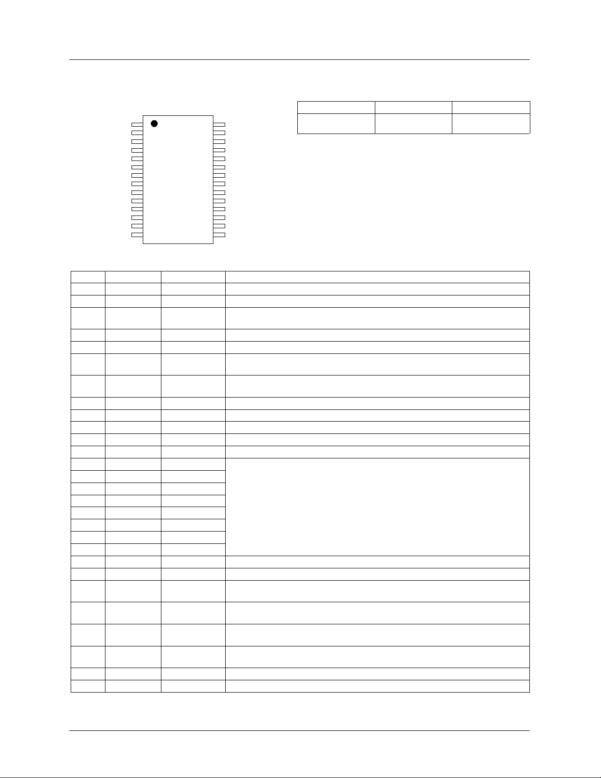
PIN CONFIGURATION ORDERING INFORMATION
DEVICE TEMP. RANGE PACKAGE
RINP
AGND2
DVDD1
OEB
VSMP
RLC
MCLK
DGND
SEN
DVDD2
SDI
SCK
OP[0]
OP[1]
1
2
3
4
5
6
7
8
9
10
11
12
13
14
WM8146
GINP
28
BINP
27
VRLC
26
VMID
25
VRT
24
VRB
23
AGND1
22
AVDD
21
OP[7]
20
OP[6]
19
OP[5]
18
OP[4]
17
OP[3]
16
OP[2]
15
XWM8146CDW/V 0 to 70oC 28-pin SOIC
PIN DESCRIPTION
PIN NAME TYPE DESCRIPTION
1 RINP Analogue input Red channel input video.
2 AGND2 Supply Analogue ground (0V).
3 DVDD1 Supply Digital supply (5V) for logic and clock generator. This must be operated at the same
4 OEB Digital i nput Output Hi-Z control, all digital outputs disabled when OEB = 1.
5 VSMP Digital input Video sample synchronisation pulse.
6 RLC Digital input Selects reset level clamp on a pixel-by-pixel basis – active high. Tie high to use on
7 MCLK Digital i nput Master clock. This clock is applied at N ti mes the input pixel rate (N = 2, 3, 6, 8 or
8 DGND Supply Digital ground (0V).
9 SEN Digital input Enables the serial interface when high.
10 DVDD2 Supply Digital supply (5V/3.3V), al l di gi tal I/O pins.
11 S DI Digital input Serial interface data input.
12 SCK Digital input Serial interface c l ock.
13 OP[0] Digital output
14 OP[1] Digital output
15 OP[2] Digital output
16 OP[3] Digital output
17 OP[4] Digital output
18 OP[5] Digital output
19 OP[6] Digital output
20 OP[7] Digital output
21 AVDD Supply Analogue s upply (5V). This must be operated at the same potential as DVDD1.
22 AGND1 Supply Analogue ground (0V).
23 VRB Analogue output Lower reference point of ADC reference stri ng
24 VRT Analogue output Upper reference poi nt of ADC reference string
25 VMID Analogue output Buffered mid-point of ADC reference string
26 VRLC Analogue output Selectable analogue output voltage for RLC.
27 BINP Analogue input Blue channel input video.
28 GINP Analogue input Green channel input video.
potential as AVDD.
every pixel.
any multiple of 2 thereaft er depending on input sample mode).
Digital multiplexed output dat a bus.
OEB = 0: ADC output data is avai l abl e i n (8+4bi t) multiplexed format on pins OP[7] to
OP[0]. See Operational Timing diagrams for details .
OEB = 1: Output is Hi=Z.
This pin must be connected to AGND via a decoupling capac i tor.
This pin must be connected to AGND via a decoupling capac i tor.
This pin must be connected to AGND via a decoupling capac i tor.
This pin must be connected to AGND via a decoupling capac i tor.
WOLFSON MICROELECTRONICS LTD
PP Rev 1.1 January 2000
2
Page 3
Product Preview
WM8146
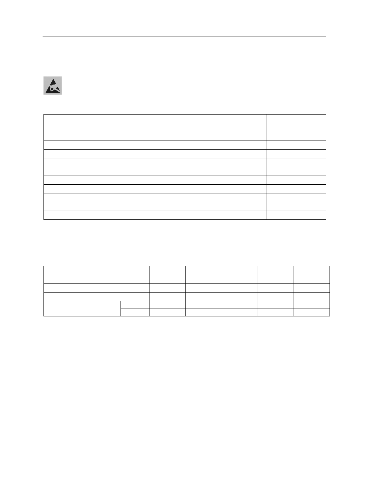
ABSOLUTE MAXIMUM RATINGS
Absolute Maximum Ratings are s tres s rat ings only. P erm anent damage to the device may be c aused by c onti nuousl y operating at
or beyond these limits. Device functional operating lim its and guaranteed performance s pecifications are gi ven under Electrical
Characteristics at the test conditions specified
ESD Sensitive Device. Thi s device i s m anufactured on a CMOS process . It i s t herefore generi cally suscept ible
to damage from excessi ve stati c voltages . Proper ES D precautions mus t be tak en during handling and st orage
of this device.
As per JEDEC specifications A112-A and A113-B, this product requires specific storage conditions prior to surface mount
assembly.
CONDITION MIN MAX
Analogue supply voltage: AVDD
Digital supply voltages: DVDD1 − 2
Digital ground: DGND
Analogue grounds: AGND1 − 2
Digital inputs, digit al outputs and digital I/O pins
Analogue inputs (RINP, GINP , BINP)
Other pins
Operating temperature range: T
Storage temperature
Lead temperature (soldering, 10 s ec)
Lead temperature (soldering, 2 mins)
Notes: 1. GND denotes the voltage of any ground pin.
2. AGND1, AGND2 and DGND pins are intended to be operat ed at the same potential. Di fferential voltages
between these pins will degrade performance.
A
GND - 0.3V GND + 7V
GND - 0.3V GND + 7V
GND - 0.3V GND + 0.3V
GND - 0.3V GND + 0.3V
GND - 0.3V DVDD2 + 0.3V
GND - 0.3V AVDD + 0.3V
GND - 0.3V AVDD + 0.3V
0°C+70
-65°C +150°C
°
+260°C
+183°C
C
RECOMMENDED OPERATING CONDITIONS
CONDITION SYMBOL MIN TYP MAX UNITS
Operating temperature range
Analogue supply voltage
Digital core supply voltage
Digital I/O supply voltage
5V I/O
3.3V I/O
T
A
AVDD 4.75 5.0 5.25 V
DVDD1 4.75 5.0 5.25 V
DVDD2 4.75 5.0 5.25 V
DVDD2 2.97 3.3 3.63 V
070
°
C
WOLFSON MICROELECTRONICS LTD
PP Rev 1.1 January 2000
3
Page 4
WM8146
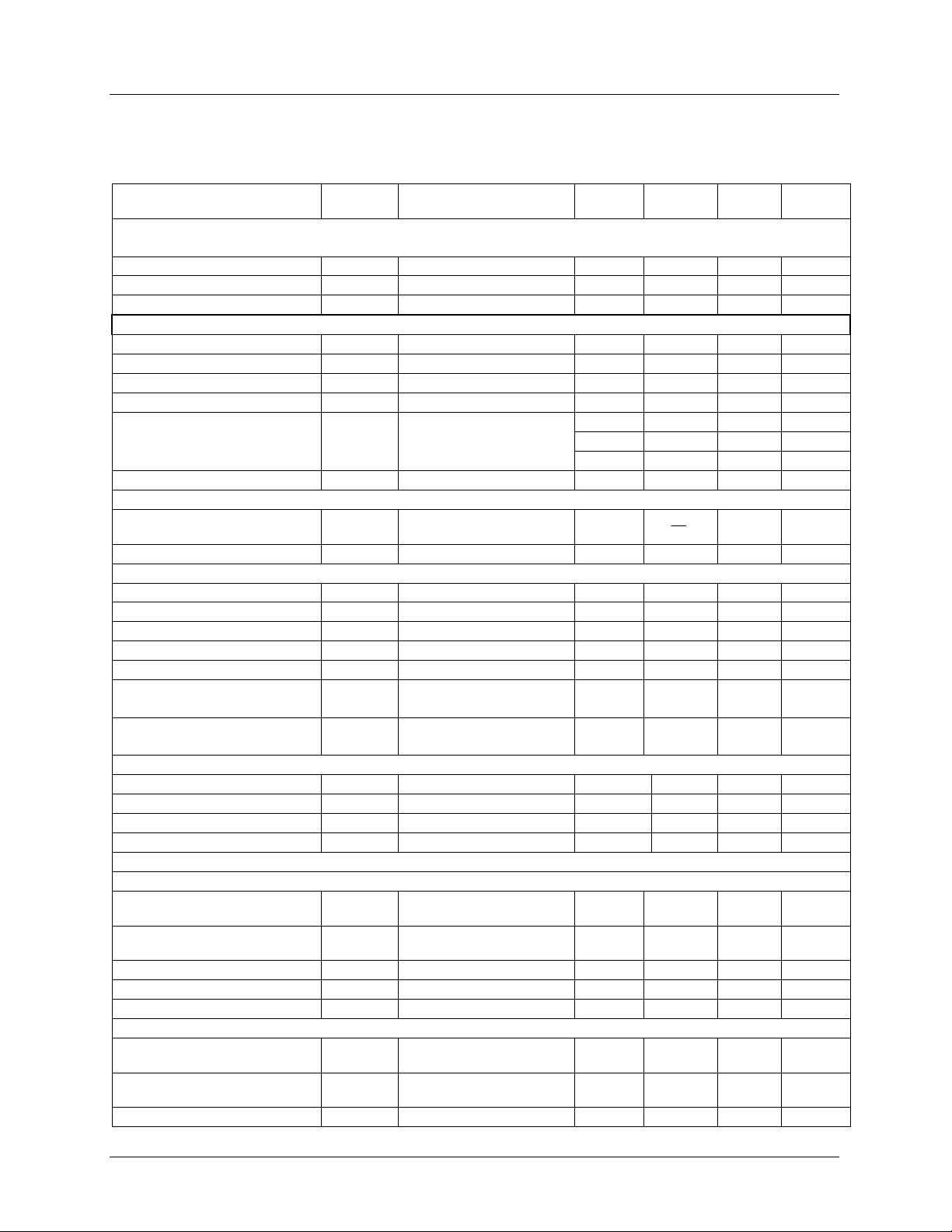
ELECTRICAL CHARACTERISTICS
Test Conditions
AVDD = DVDD1 = DVDD2 =4.75 to 5.25V, AGND = DGND = 0V, T
PARAMETER SYMBOL TEST
CONDITIONS
Overall System Specification (including 12-bit ADC, PGA, Offset and CDS functions)
NO MISSING CODES GUARANTEED
Full-scale transition error
Zero-scale transition error
Differential non-linearity
DNL +1.5 LSB
References
Upper reference voltage
Lower reference voltage
DAC reference voltage
VRT AVDD = 5V 3.47 3.5 3.53 V
VRB AVDD = 5V 1.47 1.5 1.53 V
VMID AVDD = 5V 2.47 2.5 2.53 V
RLC switching impedance
Reset level clamp opt i ons
VRLC AVDD = 5V
Voltage set by register
configuration
Impedance VRT to VRB
Input Multiplexer
CDS mode full scal e i nput range
(V
VS-VRS
)
x denotes the channel selected
Channel to channel gain matchi ng
Offset DAC (monotonicity guaranteed)
Resolution
Zero code voltage
Full scale voltage error
Differential non-linearity
Integral non-linearity
Step size
DNL 0.1 0.5 LSB
INL 0.25 1 LSB
DACRNG=0
DACRNG=1
Output voltage
DACRNG=0
DACRNG=1
Programmable Gain Amplifier (monotonicity guaranteed)
Resolution
Max gain, each channel
Min gain, each channel
G
MAX
G
MIN
Gain error, each channel
DIGITAL SPECIFICATIONS
Digital Inputs
High level input voltage
Low level input voltage
High level input current
Low level input current
Input capacitance
V
IH
V
IL
I
IH
I
IL
C
I
Digital Outputs
High level output voltage
Low level output voltage
High impedance output current
V
OH
V
OL
I
OZ
= 0 to 70°C, MCLK = 12MHz unless otherwise stated.
A
8 (+sign) bits
VMID-20 VMID+20 mV
DVDD2
IOH = 1mA DVDD2 -
IOL = 1mA DGND +
Product Preview
MIN TYP MAX UNIT
±25 ±100 mV
±25 ±100 mV
500
Ω
1.46 1.5 1.54 V
2.46 2.5 2.54 V
3.46 3.5 3.54 V
250 500 750
2
Gx
1
Ω
Vp-p
%
020mV
4.9
7.4
+/-1.25
+/-1.875
mV/step
mV/step
V
V
5bits
8.25 V/V
0.5 V/V
1%
∗
0.8
0.2
∗
V
V
DVDD2
1
1
µ
A
µ
A
5pF
V
0.5
V
0.5
1
µ
A
WOLFSON MICROELECTRONICS LTD
PP Rev 1.1 January 2000
4
Page 5
Product Preview
WM8146
Test Conditions
AVDD = DVDD1 = DVDD2 =4.75 to 5.25V, AGND = DGND = 0V, T
PARAMETER SYMBOL TEST
= 0 to 70°C, MCLK = 12MHz unless otherwise stated.
A
MIN TYP MAX UNIT
CONDITIONS
Supply Currents
Total supply current − active
Supply current − full power down
35 mA
5mA
mode
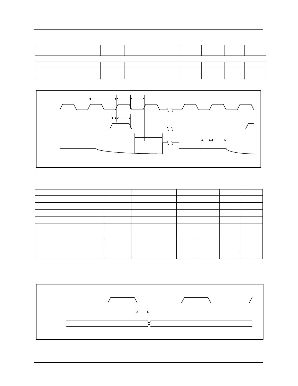
INPUT VIDEO SAMPLING
t
PER
MCLK
t
VSMPSU
VSMP
INPUT
VIDEO
Figure 1 Input Video Timing
Test Conditions
AVDD = DVDD1 = DVDD2 = 4.75 to 5.25V, AGND = DGND = 0V, T
PARAMETER SYMBOL TEST CONDITIONS MIN TYP MAX UNITS
MCLK period
MCLK high period
MCLK low period
VSMP set-up time
VSMP hold time
Video level set-up tim e
Video level hold time
Reset level set-up time
Reset level hold time
Notes:
1. t
VSU
and t
denote the set-up time requi red af ter the input video signal has settled.
RSU
t
PER
t
MCLKH
t
MCLKL
t
VSMPSU
t
VSMPH
t
VSU
t
VH
t
RSU
t
RH
2. Parameters are measured at 50% of the rising/falling edge.
t
MCLKH
t
VSMPH
t
MCLKL
t
VSUtVH
t
RSUtRH
= 0 to 70°C, MCLK = 12MHz unless otherwise stated
A
83.3 ns
37.5 ns
37.5 ns
10 ns
10 ns
10 ns
15 ns
10 ns
15 ns
OUTPUT DATA TIMING
MCLK
OP[7:0]
Figure 2 Output Data Timing
WOLFSON MICROELECTRONICS LTD
t
PD
PP Rev 1.1 January 2000
5
Page 6
WM8146
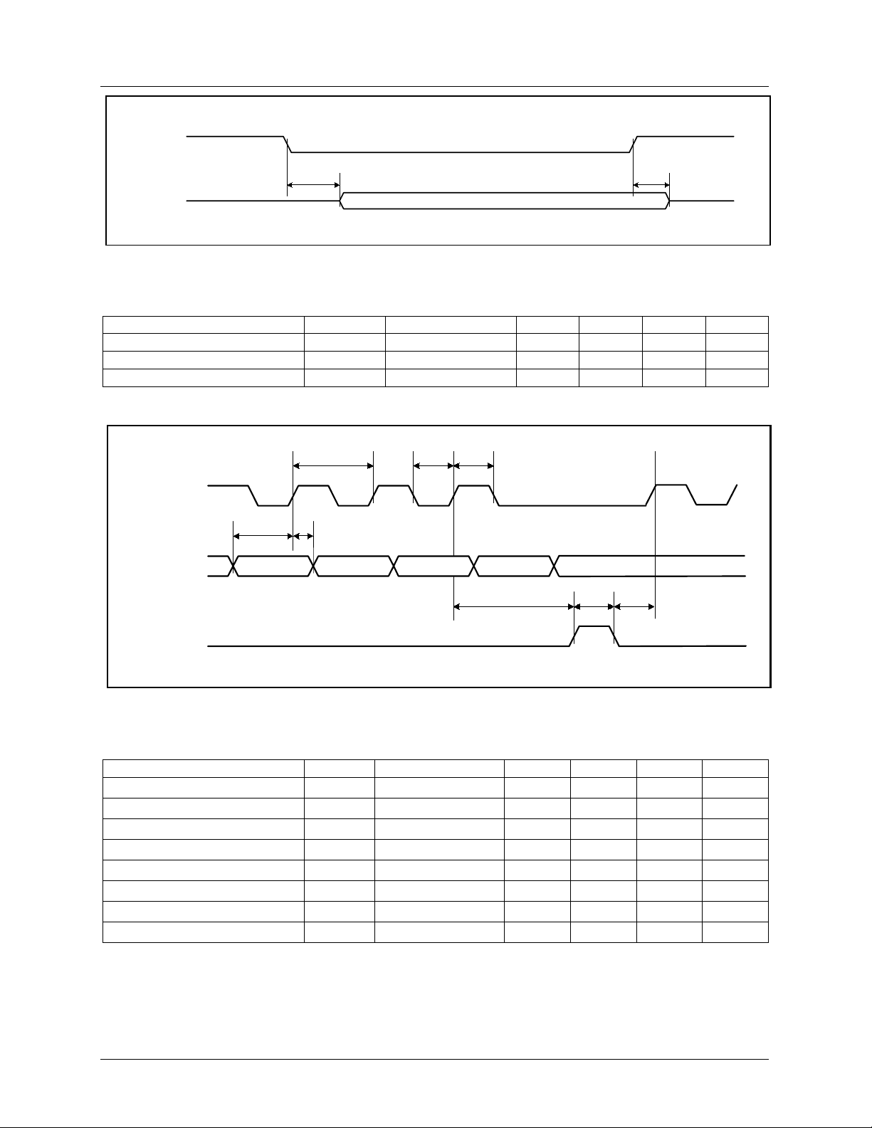
OEB
Product Preview
OP[7:0]
Hi-Z
t
PZE
t
PEZ
Hi-Z
Figure 3 Output Data Enable Timing
Test Conditions
AVDD = DVDD1 = DVDD2 = 4.75 to 5.25V, AGND = DGND = 0V, T
= 0 to 70°C, MCLK = 12MHz unless otherwise stated
A
PARAMETER SYMBOL TEST CONDITIONS MIN TYP MAX UNITS
Output propagation delay t
Output enable time t
Output disable time t
PD
PZE
PEZ
I
OH
= 1mA, I
= 1mA 75
OL
50
25
SERIAL INTERFACE
SCK
SDI
t
SSU
t
SPER
t
SH
t
SCKLtSCKH
ns
ns
ns
t
SCE
t
SEWtSEC
SEN
Figure 4 Serial Interface Timing
Test Conditions
AVDD = DVDD1 = DVDD2 = 4.75 to 5.25V, AGND = DGND = 0V, T
PARAMETER SYMBOL TEST CONDITIONS MIN TYP MAX UNITS
SCK period
SCK high
SCK low t
SDI set-up time
SDI hold time
SCK to SEN set-up time
SEN to SCK set-up time
SEN pulse width
Parameters are meas ured at 50% of the rising/falli ng edge.
Note:
t
SPER
t
SCKH
SCKL
t
SSU
t
SH
t
SCE
t
SEC
t
SEW
= 0 to 70°C, MCLK = 12MHz unless otherwise stated
A
83.3 ns
37.5 ns
37.5 ns
10 ns
10 ns
20 ns
20 ns
50 ns
WOLFSON MICROELECTRONICS LTD
PP Rev 1.1 January 2000
6
Page 7
Product Preview
DEVICE DESCRIPTION
GENERAL OPERATION
A block diagram of t he devi ce showing the signal path is present ed on P age 1.
The WM8146 samples the three inputs (RINP , GINP and BINP) simultaneously. The device then
processes the sam pled video si gnal with respect to the video res et l evel or the ref erence l evel VMID
using three processing channel s.
Each processing channel consists of an input sampling block with optional reset level clamping
(RLC) and correlated double sampling (CDS), a 5-bit programmable gain ampl ifier (PGA) and an 8bit (+sign) programmable offset DAC.
For colour operation, the resulti ng analogue outputs from the three channels are mult iplexed into a
12-bit ADC. For monochrom e operation t he res ulti ng analogue output from the s elec ted channel onl y
is multiplexed into the ADC. The ADC t hen convert s t he analogue s ignal t o a 12-bit di gital word. The
digital output from t he ADC is presented on an 8-bit wide output bus, i n 8+4-bi t multiplexed format.
Internal control registers determine the configuration of the device, including the gain and offset
applied to each channel. These registers are programmable via t he serial interface.
RESET LEVEL CLAMPING (RLC)
CONFIGURATION
To ensure that the signal applied t o the W M8146 lies within it s i nput range, the CCD output si gnal is
usually level shifted by a.c . coupling through a capac itor, C
side of this capaci tor to a selected voltage during t he CCD reset level. The RLC voltage VRLC, is
selected by control bit s RLC[1:0] in setup regist er 3.
WM8146
The RLC circuit clamps the WM8146
IN.
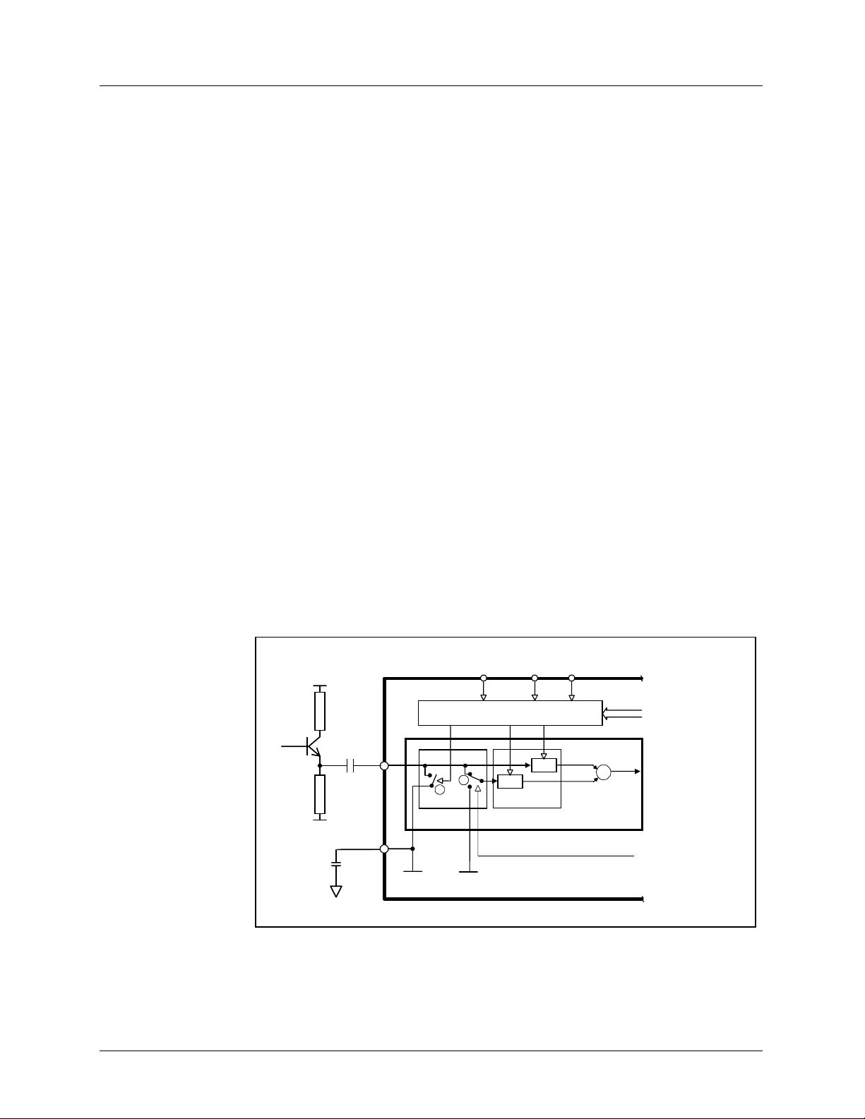
A typical input configuration dem onst rating reset level cl amping and CDS circui try is s hown in Figure
5. A clamp pulse, CL, is generated from MCLK and VS MP by the timing control block. W hen CL is
active the voltage on the WM8146 side of C
, at RINP, is forced t o the RLC voltage V RLC by switch
IN
1. When the CL pulse turns off, the voltage at RINP initially remains at VRLC but any subsequent
variation in sensor voltage (from reset to video level) will couple through C
to RINP.
IN
Reset level clamping i s compatible with both CDS and non-CDS operating modes, as select ed by
switch 2.
MCLK VSMP
TIMING CONTROL
R
S
S/H
S/H
V
S
+
+
-
INPUT SAMPLING
BLOCK FOR RED
CHANNEL
CDS
FROM CONTROL
INTERFACE
TO PGA
FROM CONTROL
INTERFACE
AGND
C
IN
RINP
VRLC
1
VRLC
RLC
CL
2
RLC CDS
VMID
Figure 5 Reset Level Clamping and CDS Circuitry
WOLFSON MICROELECTRONICS LTD
PP Rev 1.1 January 2000
7
Page 8
WM8146
Product Preview
TIMING
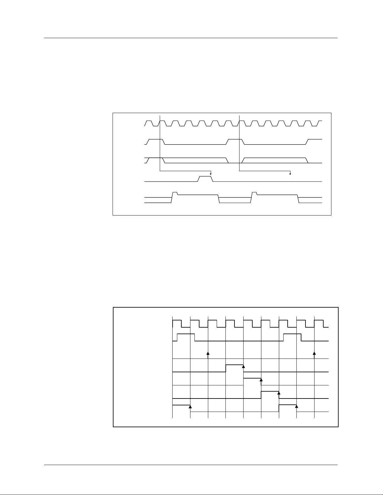
Figure 6 illustrates the use of the RLC pin, MCLK and VSMP to control the timing of the CL pulse f or
a typical CCD waveform. The CL pulse i s applied during the reset period.
The input signal applied to the RLC pin is sampled on t he positive edge of MCLK that oc curs during
each VSMP pulse. The sampled level, high (or low) controls the presence (or absence) of the internal
CL pulse on the next reset level. The position of CL can be adjusted by using control bits
CDSREF[1:0], as shown in Figure 7.
The VRLC pin outputs the analogue RLC voltage s el ected via control set-up register 3 bits RLC[1:0].
MCLK
VSMP
RLC
(CDSREF = 01)
INPUT VIDEO
Figure 6 Relationship of RLC Pin, MCLK and VSMP to Internal Clamp Pulse, CL
CDS/NON-CDS PROCESSING
For CCD type input signals, the signal may be processed using CDS, which will remove pixel-by-pixel
common mode noise. For CDS operation, the video l evel is proc ess ed with respec t t o the vi deo reset
level, regardless of whether RLC has been perform ed. To s ample using CDS, cont rol bit CDS must
be set to 1 (default), this controls switc h 2 (Figure 5) and causes the si gnal reference to come from
the video reset level. The tim e at which the reset level is sampled, by cl ock R
programming control bits CDSREF[1:0], as s hown in Figure 7 .
For CIS type sensor signals , non-CDS process ing is used. I n this cas e, the video level is proc essed
with respect to the reference voltage VMID.
1X X0X X 0
Programmable Delay
CL
RGB RGB
No RLC on this PixelRLC on this Pixel
/CL, is adjustable by
s
MCLK
VSMP
RGB
R
/CL (CDSREF = 00)
S
/CL (CDSREF = 01)
R
S
/CL (CDSREF = 10)
R
S
/CL (CDSREF = 11)
R
S
Figure 7 Reset Sample and Clamp Timing
WOLFSON MICROELECTRONICS LTD
VS
PP Rev 1.1 January 2000
8
Page 9
Product Preview
g
OFFSET ADJUST AND PROGRAMMABLE GAIN
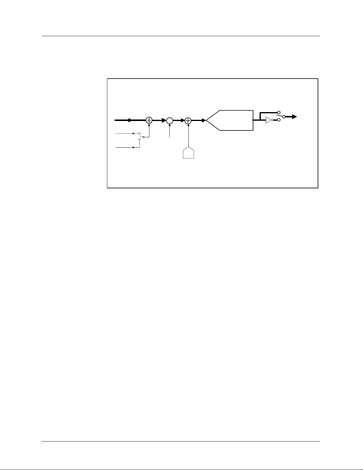
The output from the CDS bloc k is a diff erential signal, which is am plified by a 5-bit PGA t hen added
to the output of an 8-bit (+sign) offset DAC to com pensate for sensor d.c. offsets. The gain and offset
for each channel are independently programm able by writing to control bi ts DAC[7: 0] and PGA[ 4:0].
The following diagram shows the signal pat h t hrough the device.
WM8146
OUTPUT
INVERT
BLOCK
D
1
digital
D2 = D1 if INVOP = 0
D2 =4095-D1 if INVOP = 1
is VIN sampled during reset clamp
TO MULTIPLEXER
FOR 8-BIT OUTPUT
D
2
V
V
V
IN
RESET
MID
INPUT
SAMPLING
BLOCK
+
CDS = 1
CDS = 0
(1-2*DSIGN)*(DAC[7:0]/255)*(V
PGA
BLOCK
V
1
-
PGA gain
A = 0.5+(PGA[4:0]*0.25)
V
X
OFFSET DAC
BLOCK
V
2
+
+
Offset
DAC
/2 + V
MID
3
analo
/4*DACRNG)
MID
ADC BLOCK
V3 x (4096/VFS) +2047
is RINP or GINP or BINP
V
IN
V
RESET
is AVDD/2
V
MID
CDS, DAC[7:0], DSIGN, DACRNG, PGA[4:0]
and INVOP are set by programming internal
control registers.
CDS=1 for CDS, 0 for non-CDS
Figure 8 Signal Flow Diagram
The following equations enable the user to calculate the set tings required for the PGAs and offset
DACs.
INPUT SAMPLING AND REFERENCING
If CDS=1, the previously sam pled reset level, V
(i.e. CDS operation).
V
= VIN - V
1
If CDS=0, the sim ul taneously sampled V
RESET
is subtracted inst ead (i .e. non-CDS operation).
MID
, is subtracted from the input video signal V
RESET
IN
V
= VIN - V
1
MID
GAIN ADJUST
The signal is then mult i pl i ed by the PGA gain, approximately 0.5 to 8.25 in 32 equal gain steps.
V
= V1 * G
2
= V
* (0.5+(PGA[4:0]*0.25))
1
OFFSET (BLACK-LEVEL) ADJUST
The resultant signal is added t o the Offset DAC output which has a range of VMID/2 (or 1.5*VMID/2 if
the DACRNG bit is set).
V
= V2 + V
3
= V
+ [(1-2*DSIGN) * DAC_CODE/255 * (VMID/2 + VMID/4 * DACRNG)]
2
DAC
ANALOGUE TO DIGITAL CONVERSION
The analogue signal is then converted to a 12-bit unsigned number. This is equivalent to a
multiplicati on by 4096/(V
D
== INT{ (V3/VFS) * 4096 } + 2047
1
At this stage, t he input to the ADC should be bet ween -1V and +1V, so D
-2047 and +2048. If the input is over-range, it will be clipped to within the range (-2047,2048).
2047 is added to the ADC output, to give code 2047 for zero input signal to the ADC. This is
equivalent to the +VMID shown in the block diagram on page 1.
), where VFS = 2V .
FS
[11:0] should lie between
1
WOLFSON MICROELECTRONICS LTD
PP Rev 1.1 January 2000
9
Page 10
WM8146
DIGITAL POLARITY ADJUST
The polarity of the digital output m ay be inverted by control bit INVOP . If INVOP=0, negative-goi ng
input video will give negative-going digital output. If INVOP=1, negative-going video will give pos itivegoing digital output.
D
= D1 … (INVOP=0)
2
D
= 4095 – D1 … (INVOP=1)
2
DIGITAL CONTROL AND I/O FUNCTIONS
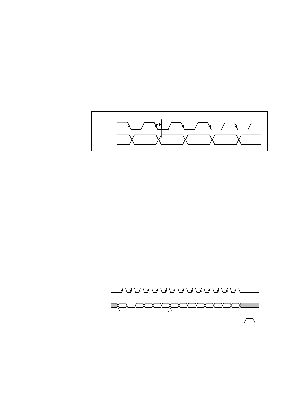
OUTPUT DATA
Data appears on the pins
Figure 9 .
MCLK
OP[7:0]
and changes after every negative-going
t
PD
Product Preview
edge, as shown in
MCLK
Figure 9 WM8146 Output Timing
A = d11, d10, d9, d8, d7, d6, d5, d4 Pin OP[7] to OP[0]
B = d3, d2, d1, d0, 0, CC[1], CC[0], OVRNG Pin OP[7] to OP[0]
Where
CC1/CC0: These bits show from which channel the current output was taken. 00 = RED,
01 = GREEN, 10 = BLUE.
OVRNG: This bit indicates if the current output pixel has exceeded the maxim um or m inimum range
during processing. 1 = out of range, 0 = withi n range.
CONTROL INTERFACE
The internal control registers are programmable via the serial di gi t al control interface.
REGISTER WRITE
The serial interface involves three dedicated pins,
address is clocked i n through
bit is latched on the rising edge of
applied to
address bit a4 equal to 0.
OP[7:0]
SEN
AB
MSB first followed by an eight-bit data word, also MSB firs t. E ach
SDI
to transfer the data to the appropriate internal register. Not e all valid registers have
. Once the data has been shift ed into the device, a pulse is
SCK
SCK, SDI, SEN
(refer to Figure 10). A six-bit
SCK
SDI
SEN
Figure 10 Register Write Timing
TIMING REQUIREMENTS
To use this device a master clock (MCLK) of up to 12MHz and a per-pixel synchronis ation clock
(VSMP) of up to 6MHz are required. These clocks drive a timing control block, which produces
WOLFSON MICROELECTRONICS LTD
a5 0 a3a2a1a0b7b6b5b4b3b2b1b0
Address Data Word
PP Rev 1.1 January 2000
10
Page 11

Product Preview
internal signals to cont rol the sampling of the video signal. MCLK to VSMP ratios and maximum
sample rates for the vari ous modes are shown in Table 1.
POWER SUPPLY
The WM8146 can run from a 5V single supply or from split 5V (core) and 3.3V (digital interface)
supplies.
OPERATING MODES
Table 1 summarises t he m ost com m onl y used m odes , t he cl ock waveform s required and t he regis ter
contents required for CDS and non-CDS operat i on.
MODE DESCRIPTION CDS
1 Colour
Pixel-by-Pixel
2 Monochrome/
Colour
Line-by-Line
3Fast
Monochrome/
Colour
Line-by-Line
4 Maximum
speed
Monochrome/
Colour
Line-by-Line
5 Slow Colour
Pixel-by-Pixel
6Slow
Monochrome/
Colour
Line-by-Line
Table 1 WM8146 Operating Modes
AVAILABLE
Yes 2MSPS The 3 input channels
Yes 2MSPS As mode 1 except:
Yes 4MSPS Identical to mode 2 MCLK max =
No 6MSPS Identi cal to mode 2 MCLK max =
Yes 1.5MSPS Identi cal to mode 1 MCLK max =
Yes 1.5MSPS Identi cal to mode 2 MCLK max =
MAX
SAMPLE
RATE
SENSOR
INTERFACE
DESCRIPTION
are sampled in
parallel. The signal is
then gain and offset
adjusted before being
multiplexed into a
single data stream and
converted by the ADC,
giving an output data
rate of 6MSPS max.
Only one input
channel at a time
is continuously
sampled.
TIMING
REQUIRE-
MENTS
MCLK max =
12MHz
MCLK:VSMP
ratio is 6:1
MCLK max =
12MHz
MCLK:VSMP
ratio is 6:1
12MHz
MCLK:VSMP
ratio is 3:1
12MHz
MCLK:VSMP
ratio is 2:1
12MHz
MCLK:VSMP
ratio is
2n:1, n ≥ 4
12MHz
MCLK:VSMP
ratio is
2n:1, n ≥ 4
REGISTER
CONTENTS
WITH
CONTROL
BIT CDS=1
SetReg1:
03(hex)
SetReg1:
07(hex)
SetReg3 bits
7:6
determine
which input is
to be
sampled
Identical to
mode 2 plus
SetReg3: bits
5:4 must be
set to 0(hex)
CDS not
possible
Identical to
mode 1
Identical to
mode 2
WM8146
REGISTER
CONTENTS
WITH
CONTROL
BIT CDS=0
SetReg1:
01(hex)
SetReg1:
05(hex)
SetReg3
bits 7:6
determine
which input
is to be
sampled
Identical to
mode 2
SetReg1:
45(hex)
SetReg3
bits 7:6
determine
which input
is to be
sampled
Identical to
mode 1
Identical to
mode 2
WOLFSON MICROELECTRONICS LTD
PP Rev 1.1 January 2000
11
Page 12
WM8146
OPERATING MODE TIMING DIAGRAMS
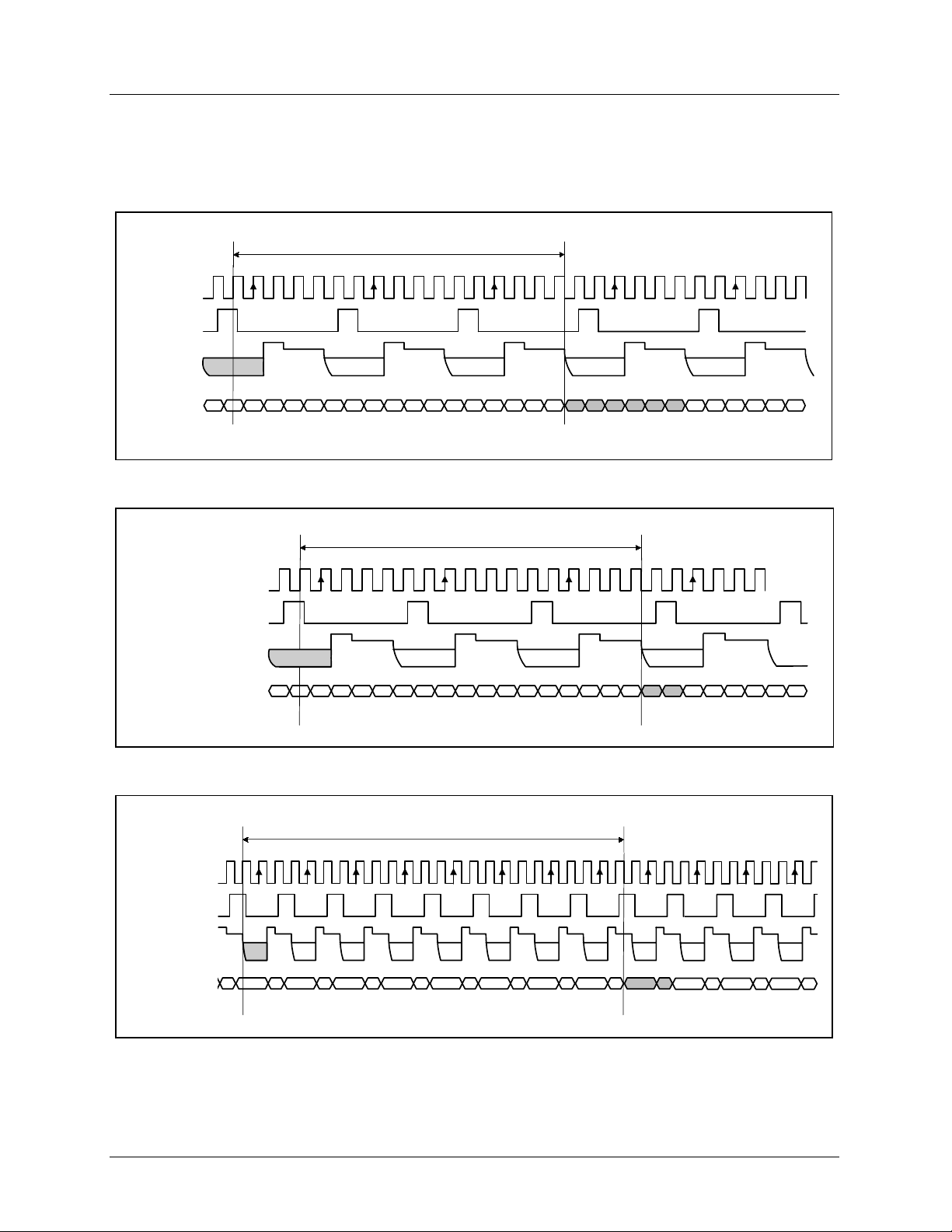
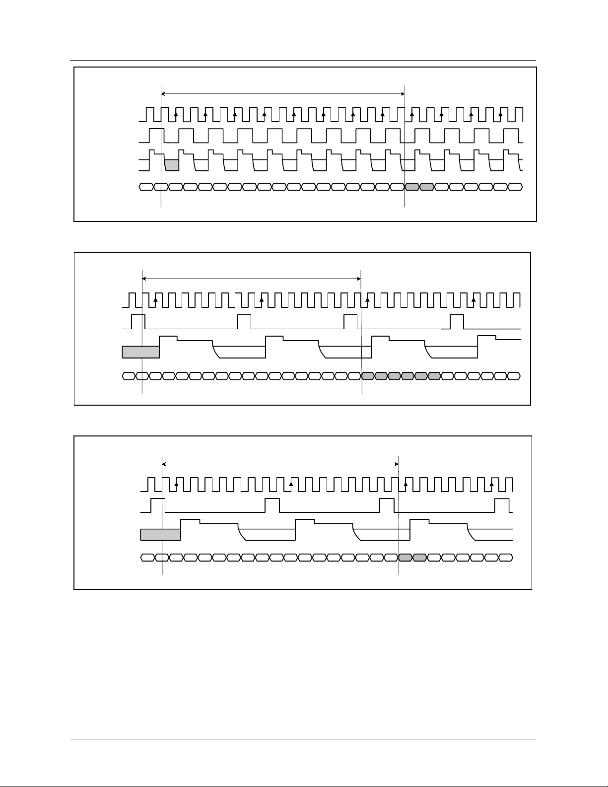
The following diagrams output data, MCLK, VSMP and input vi deo requirements f or operation of the
most commonl y used modes as shown in Table 1 . The diagrams are identic al for both CDS and
non-CDS operation. Outputs from RINP, GINP and BINP are s hown as R, G and B respectively. X
denotes invalid data.
16.5 MCLK PERIODS
MCLK
VSMP
INPUT
VIDEO
Product Preview
OP[7:0]
RARBGAGBBABBRARBGAGBBABBRARBGAGBBAB
Figure 11 Mode 1 Operation
MCLK
VSMP
INPUT VIDEO
OP[7:0]
Figure 12 Mode 2 Operation
RAR
GAGBBAB
RARBGAGBBAB
B
RAR
B
B
B
16.5 MCLK PERIODS
X
X X X
B
RAR
X X X X
B
RAR
X X X X
B
RAR
X X X X
B
RAR
B
23.5 MCLK PERIODS
MCLK
VSMP
INPUT VIDEO
OP[7:0]
RBRARBRARBRARBRARBRARBRARBRARBRARBRAR
Figure 13 Mode 3 Operation
WOLFSON MICROELECTRONICS LTD
RARBRARBRAR
B
PP Rev 1.1 January 2000
B
12
Page 13
Product Preview
MCLK
VSMP
INPUT VIDEO
WM8146
16.5 MCLK PERIODS
OP[7:0]
RARBRARBRARBRARBRARBRARBRARBRARBRARBRARBRARBRARBRAR
Figure 14 Mode 4 Operation
16.5 MCLK PERIODS
MCLK
VSMP
INPUT
VIDEO
OP[7:0]
RARBGAGBBAB
X X
B
RARBGAGBBAB
X X
Figure 15 Mode 5 Operation (MCLK:VSMP Ratio = 8:1)
16.5 MCLK PERIODS
B
B
B
RARBGAGBBAB
X X
X X
RARBGAG
B
MCLK
VSMP
INPUT VIDEO
OP[7:0])
X X
X X X X X X
B
RAR
Figure 16 Mode 6 Operation (MCLK:VSMP Ratio = 8:1)
WOLFSON MICROELECTRONICS LTD
RAR
X X X X X X
B
RAR
X X X X X X
B
PP Rev 1.1 January 2000
13
Page 14

WM8146
DEVICE CONFIGURATION
REGISTER MAP
Table 2 describes the location of each c ontrol bit used to determ ine the operation of the W M8146.
The register map is program med by writing the required c odes to t he appropriate address es via the
serial interface.
Product Preview
Description Def
<a5:a0>
000001 Setup Register 1 03 VSMP6M MONO CDS ENADC
000010 Setup Register 2 00 INVOP
000011 Setup Register 3 11 CHAN[1] CHAN[0] CDSREF[1] CDSREF[0] RLC[1] RLC[0]
000100 Software Reset 00
000101 Setup Register 4 00 DACRNG
100000 DAC Value (Red) 00 DAC[7] DAC[6] DAC[5] DAC[4] DAC[3] DAC[2] DAC[1] DAC[0]
100001 DAC Value (Green) 00 DAC[7] DAC[6] DAC[5] DAC[4] DAC[3] DAC[2] DAC[1] DAC[0]
100010 DAC Value (Blue) 00 DAC[7] DAC[6] DAC[5] DAC[4] DAC[3] DAC[2] DAC[1] DAC[0]
100011 DAC Value (R+G+B) 00 DAC[7] DAC[6] DAC[5] DAC[4] DAC[3] DAC[2] DAC[1] DAC[0]
100100 DAC Sign (Red) 00 DSIGN
100101 DAC Sign (Green) 00 DSIGN
100110 DAC Sign (Blue) 00 DSIGN
100111 DAC Sign (R+G+B) 00 DSIGN
101000 PGA Gain (Red) 00 PGA[4] PGA[3] PGA[2] PGA[1] PGA[0]
101001 PGA Gain (Green) 00 PGA[4] PGA[3] PGA[2] PGA[1] PGA[0]
101010 PGA Gain (Blue) 00 PGA[4] PGA[3] PGA[2] PGA[1] PGA[0]
101011 PGA Gain (R+G+B) 00 PGA[4] PGA[3] PGA[2] PGA[1] PGA[0]
(hex)
b7 b6 b5 b4 b3 b2 b1 b0
BITAddress
Table 2 Register Map
WOLFSON MICROELECTRONICS LTD
PP Rev 1.1 January 2000
14
Page 15

Product Preview
REGISTER MAP DESCRIPTION
REGISTER BITNOBIT NAME(S) DEFAULT DESCRIPTION
WM8146
Setup
Register 1
Setup
Register 2
Setup
Register 3
Software
Reset
Setup
Register 4
Registers
100100 to
100111
Table 3 Register Control Bits
0 ENADC 1
1 CDS 1
2MONO 0
6 VSMP6M 0
2INVOP 0
1:0 RLC[1:0] 01
5:4 CDSREF[1:0] 01
7:6 CHAN[1:0] 00
1 DACRNG 0
0DSIGN 0
ADC standby control : 0=standby, 1=active
Select correlated double sampling mode:
0=single ended mode, 1=CDS m ode
Mono/colour select: 0=colour, 1=monchrome operation
Required when VSMP at 6MSPS:
0=other mode, 1=VSMP at 6MSPS
Digitally inverts the polari ty of input data.
0= negative going video gives negative going output,
1=negative-going video gives positive going out put data.
Reset Level Clamp Voltage:
00 = 1.5V; 01 = 2.5V; 10 = 1.5V; 11 = Reserved
CDS mode reset timing adjust
00 = advance 1 MCLK period
01 = Normal
10 = Retard 1 MCLK period
11 = Retard 2 MCLK periods
Monochrome mode channel select
00 = Red channel select
01 = Green channel select
10 = Blue channel select
11 = Reserved
Write any value to t he Software Reset register to cause all
cells to be reset.
Offset DAC Output Range:
0 = DAC Output range =VMID/2 = +/-1.25V
1 = DAC output Range = 1.5*VMID/2 = +/-1.875V
Polarity of Offset DA C output
0 = Positive Output (Offs et added)
1 = Negative Output (Offset removed)
WOLFSON MICROELECTRONICS LTD
PP Rev 1.1 January 2000
15
Page 16
WM8146
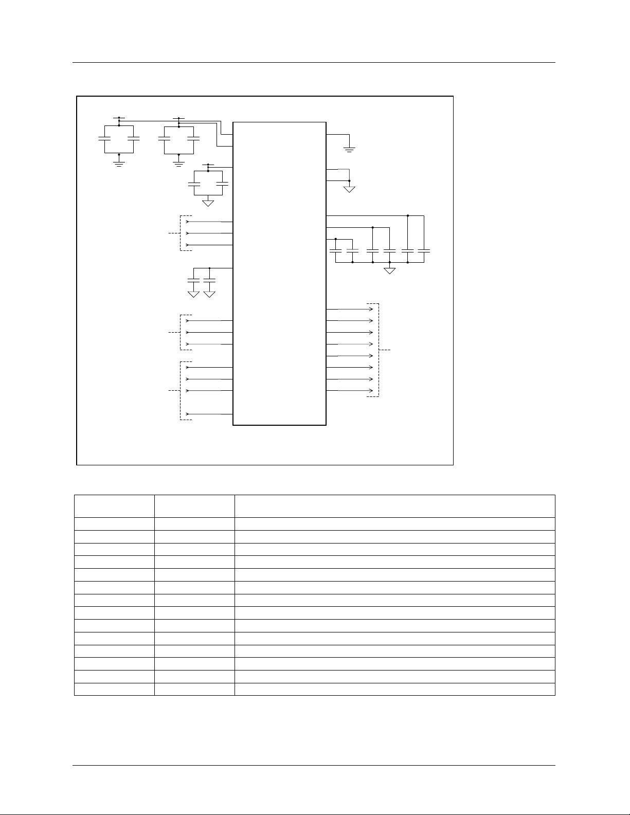
RECOMMENDED EXTERNAL COMPONENTS
DVDD1 (5V) DVDD2 (3.3V or 5V)
Product Preview
C1 C2
VIDEO
INPUTS
TIMING
SIGNALS
INTERFACE
CONTROLS
C3 C4
AVDD (5V)
C5
C13
AGND
C14
AGND
3
10
21
C6
1
28
27
26
7
5
6
12
11
9
4
DVDD1
DVDD2
AVDD
RINP
GINP
BINP
VRLC
WM8146
MCLK
VSMP
RLC
SCK
SDI
SEN
OEB
DGND
AGND1
AGND2
VRT
VMID
VRB
OP[7]
OP[6]
OP[5]
OP[4]
OP[3]
OP[2]
OP[1]
OP[0]
8
22
2
AGND
24
25
23
C8 C10 C12C9
C7 C11
AGND
20
19
18
17
16
15
14
13
OUTPUT
DATA
BUS
C1-14 should be fitted as close to WM8146 as possible.NOTES:
1.
AGND and DGND should be connected as close to WM8146 as possible.
2.
Figure 17 External Components Diagram
COMPONENT
REFERENCE
SUGGESTED
VALUE
C1 100nF
C2 10µF
C3 100nF
C4 10µF
C5 100nF
C6 10µF
C7 100nF
C8 10µF
C9 100nF
C10 22µF
C11 100nF
C12 10µF
C13 100nF
C14 10µF
Table 4 External Components Descriptions
DESCRIPTION
De-coupling for DVDD1.
Reservoir capacitor for DVDD1.
De-coupling for DVDD2.
Reservoir capacitor for DVDD2
De-coupling for AVDD.
Reservoir capacitor for AV DD
De-coupling for VRB..
Reservoir capacitor for VRB .
De-coupling for VMID
Reservoir capacitor for VMID.
De-coupling for VRT
Reservoir capacitor for VRT
De-coupling capacitor for VRLC
Reservoir capacitor VRLC
WOLFSON MICROELECTRONICS LTD
PP Rev 1.1 January 2000
16
Page 17
Product Preview
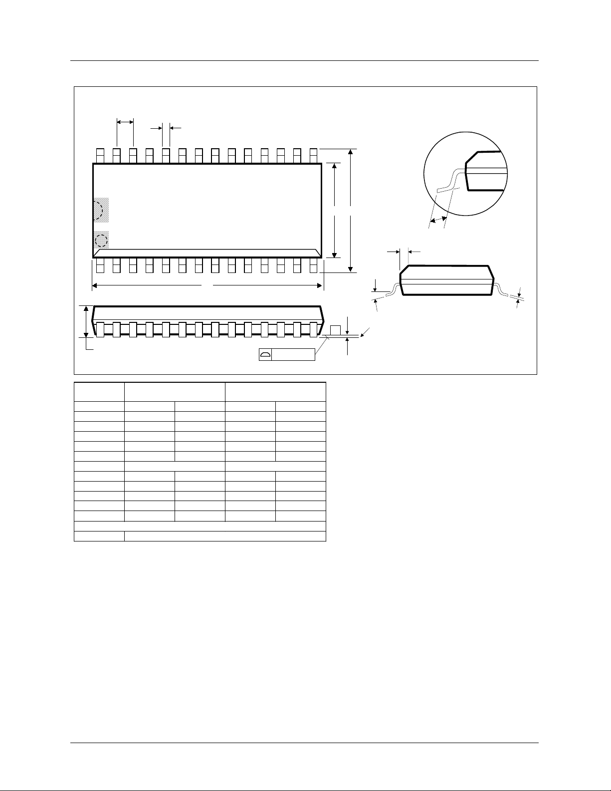
PACKAGE DIMENSIONS
WM8146
D: 28 PIN SOICW 7.5mm (0.3") Wide Body, 1.27mm Lead Pitch
e
28
ZONE A
ZONE B
1
A
B
15
E H
14
D
A1
-C-
0.10 (0.004)
α
SEATING PLANE
L
h x 45
DM016.B
o
C
Symbols
Dimensions
(mm)
Dimensions
(Inches)
MIN MAX MIN MAX
A
A
1
B
C
D
e
E
h
H
L
α
REF:
NOTES:
A. ALL LINEAR DIMENSIONS ARE IN MILLIMETERS (INCHES).
B. THIS DRAWING IS SUBJECT TO CHANGE WITHOUT NOTICE.
C. BODY DIMENSIONS DO NOT INCLUDE MOLD FLASH OR PROTRUSION, NOT TO EXCEED 0.25MM (0.010IN).
D. MEETS JEDEC.95 MS-013, VARIATION = AE. REFER TO THIS SPECIFICATION FOR FURTHER DETAILS.
E. PIN ONE INDICATORS WILL BE LOCATED IN EITHER ZONE A OR ZONE B.
2.35 2.65 0.0926 0.1043
0.10 0.30 0.0040 0.0118
0.33 0.51 0.0130 0.0200
0.23 0.32 0.0091 0.0125
17.70 18.10 0.6969 0.7125
1.27 BSC 0.0500 BSC
7.40 7.60 0.2914 0.2992
0.25 0.75 0.0100 0.0290
10.00 10.65 0.3940 0.4190
0.40 1.27 0.0160 0.0500
o
0
o
8
o
0
o
8
JEDEC.95, MS-013
WOLFSON MICROELECTRONICS LTD
PP Rev 1.1 January 2000
17
 Loading...