

Page 1
WM8144-12
Production Data
February 1998 Rev. 4.1
Integrated 12-bit Data Acquisition System for
Imaging Applications
Description
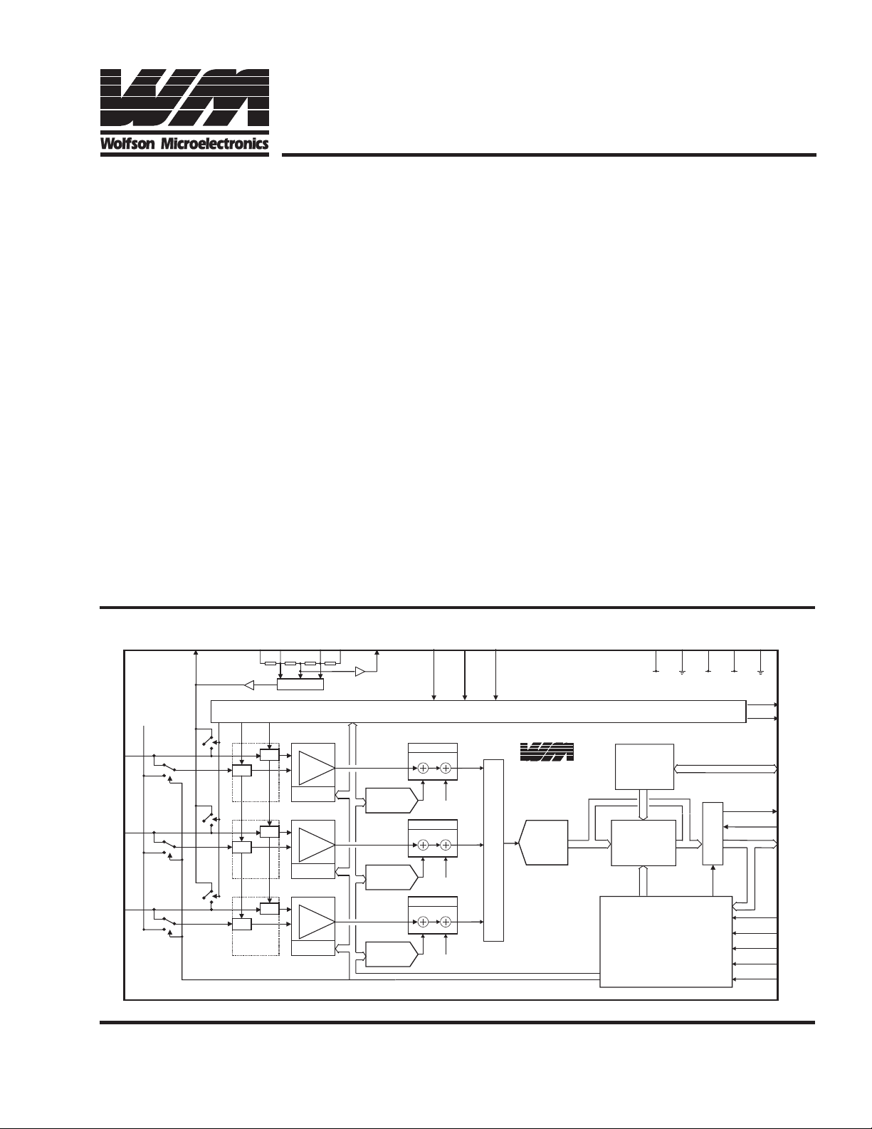
WM8144-12 integrates the analogue signal conditioning
required by CCD sensors with a 12-bit ADC and optional
pixel-by-pixel image compensation. WM8144-12 requires
minimal external circuitry and provides a cost effective
sensor-to-digital domain system solution.
Each analogue conditioning channel provides reset level
clamp, CDS, fine offset level shifting and gain
amplification. The three channels are multiplexed into the
ADC. Output from the ADC can either be direct or passed
through a digital post-processing function. The postprocessing provides compensation for variations in offset
and shading on a pixel-by-pixel basis.
The flexible output architecture allows twelve-bit data to
be accessed either on a twelve-bit bus or via a timemultiplexed eight-bit bus. The WM8144-12 can be
configured for pixel-by-pixel or line-by-line multiplexing
operation. Reset level clamp and/or CDS features can be
optionally bypassed. Device configuration is either by a
simple serial or eight-bit parallel interface.
Block Diagram
VRUV
RT
V
RB
V
RLC
RLVMID
V
VSMP
Features
• Reset level clamp
• Correlated Double Sampling (CDS)
• Fine offset level shifting
• Programmable Gain Amplification
• 12-Bit ADC with maximum 4 MSPS
• Digital post-processing for pixel-by-pixel
image compensation
• Simple clocking scheme
• Control by serial or parallel interface
• Time-multiplexed eight-bit data output mode
• 48 pin TQFP package
• Pin compatible with WM8144-10
Applications
• Document scanners
• CCD sensor interfaces
• Contact image sensor (CIS) interfaces
RLC
MCLK
A
VDDAGNDDVDD1DVDD2DGND
VS
V
MID
RINP
GINP
BINP
Production Data data sheets contain final
specifications current on publication date.
Supply of products conforms to Wolfson
Microelectronics standard terms and conditions.
RSCL
S/H
S/H
CDS
S/H
S/H
CDS
S/H
S/H
CDS
MUX
TIMING CONTROL
OFFSET
PGA
5-BIT REG
PGA
5-BIT REG
PGA
5-BIT REG
8-BIT + SIGN
DAC
8-BIT + SIGN
DAC
8-BIT + SIGN
DAC
OFFSET
OFFSET
V
MID
V
MID
V
MID
WM8144-12
M
U
X
12 BIT
ADC
Wolfson Microelectronics
Lutton Court, Bernard T errace, Edinburgh EH8 9NX, UK
Tel: +44 (0) 131 667 9386 Fax: +44 (0) 131 667 5176
email:[email protected]
www: http://www.wolfson.co.uk
EXTERNAL
DATA STORE
INTERFACE
IMAGE
COMPENSATION
PROCESSING
CONFIGURABLE
SERIAL/PARALLEL
CONTROL INTERFACE
12/8
MUX
© 1998 Wolfson Microelectronics
CC[2:0]
DV
CDATA(7:0)
ORNG
OEB
OP[11:0]
PNS
SDI / DNA
SCK / RNW
SEN / STB
NRESET
1
Page 2
WM8144-12
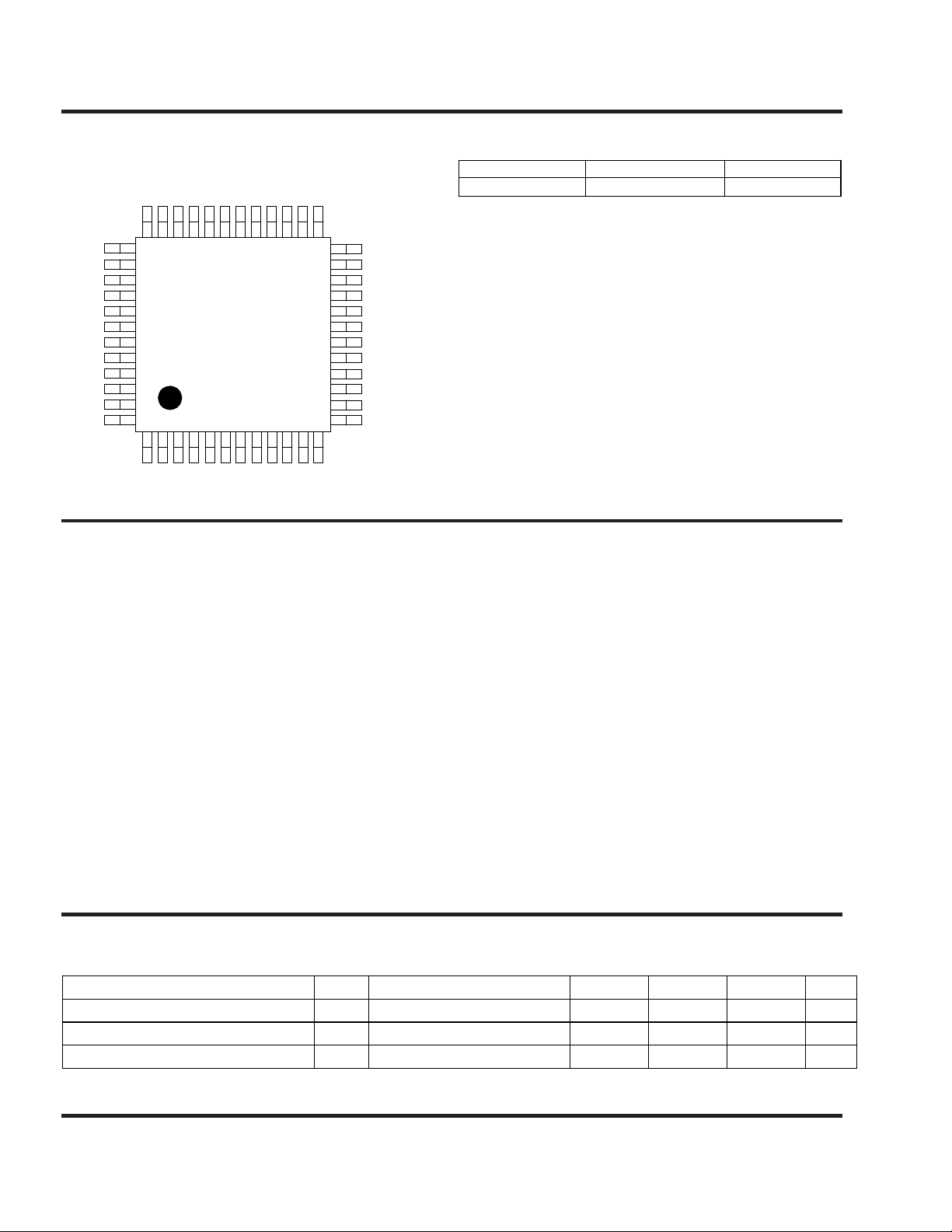
Package Outline
CDATA3
CDATA2
CDATA1
CDATA0
DGND
OP11
OP10
OP9
OP8
OP7
OP6
OP5
CDATA4
3635343332
37
38
39
40
41
42
43
44
45
46
47
48
1
OP4
CDATA7
CDATA6
CDATA5
3
4
2
OP2
OP3
DVDD2
DVDD1
VSMP
MCLK
3130292827
WM8144-12
7
6
5
DV
OP0
OP1
SDI/DNA
SCK/RNW
RLC
9
8
10
CC2
CC1
CC0
OEB
SEN/STB
25
26
24
23
22
21
20
19
18
17
16
15
14
13
12
11
ORNG
NRESET
PNS
RINP
GINP
BINP
VMID
VRLC
AGND
AVDD
VRL
VRU
VRB
VRT
Absolute Maximum Ratings
Analogue Supply Voltage. . . AGND - 0.3 V, AGND +7 V
Digital Supply Voltage. . . . DGND - 0.3 V, DGND +7 V
Digital Inputs . . . . . . . . .DGND - 0.3 V , DVDD + 0.3 V
Digital Outputs. . . . . . . .DGND - 0.3 V, DVDD + 0.3 V
Reference inputs . . . . . . AGND - 0.3 V, AVDD + 0.3 V
RINP, GINP, BINP . . . . . . AGND - 0.3 V , AVDD + 0.3 V
Ordering Information
DEVICE TEMP RANGE PACKAGE
WM8144-12CFT/V 0
Operating temperature range, T
Storage T emperature . . . . . . . . . . -50oC to +150oC
Lead T emperature (soldering, 10 sec) . . . . . . +260oC
0
C - 700C 48 Pin TQFP
A . . . . . . 0
o
C to +70oC
Note: Absolute Maximum Ratings are stress ratings only. Permanent damage to the device may be caused by
continuously operating at or beyond these limits. Device functional operating range limits and guaranteed
performance specifications are given under Electrical Characteristics at the test conditions specified.
ESD Sensitive Device. The WM8144-12 is manufactured on a CMOS process. It is therefore generically
susceptible to damage from excessive static voltages. Proper ESD precautions must be taken during handling
and storage of this device.
As per JEDEC specifications A112-A and A113-A this product requires specific storage conditions prior to
surface mount assembly. It has been classified as having a Moisture Sensitivity level of 2 and as such will be
supplied in vacuum sealed moisture barrier bags.
Recommended Operating Conditions
PARAMETER TEST CONDITIONS MIN TYP MAX UNIT
Supply Vo l tage 4.75 5.25 V
Operating Temperature Range
Input Common Mode Range
V
A
T
CMR
070
0.5 4.5 V
o
C
Wolfson Microelectronics
2
Page 3
WM8144-12
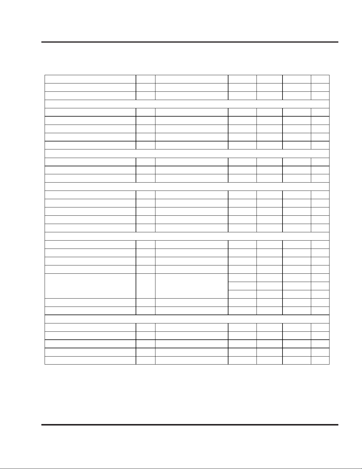
Electrical Characteristics
VDD = 4.75V to 5.25V, GND = 0 V, ........TA = 0oC to +70oC, MLCK = 8MHz unless otherwise stated.
PARAMETER TEST CONDITIONS MIN TYP MAX UNIT
Supply Current - Active 110.0 150 mA
Supply Current - Standby 10.0 15 mA
Digital Inputs
High Level Input Voltage V
Low Level Input Voltage V
High Level Input Current I
Low Level Input Current I
IH
IL
IH
IL
Input Capacitance 10.0
Digital Outputs
High Level Output Voltage V
Voltage output range V
High Impedance Output Current
OHIOH
OLIOL
OZ
I
= 1.0mA
= 1.0mA
Input Multiplexer
Channel to Channel Gain Matching
Input Video Set-up Time
Input Video Hold Time
Reset Video Set-up Time
Reset Video Hold Time
tVSU
tVH
CDS Mode only 10 ns
tRSU
CDS Mode only 25 ns
tRH
Reference String
Reference Voltage - Top
Reference Voltage - Bottom
DAC Reference Voltage
RTVRU
V
RBVRU
V
MIDVRU
V
= 5.00 V, VRL = 0.00V
= 5.00 V, VRL = 0.00V
= 5.00 V, VRL = 0.00V
R.L.C. Switch Impedence 200 Ohms
Reset Level Clamp Options
RLC
V
VRU = 5.00 V, VRL = 0.00V
Voltage set by user
configuration - Table 7
RT
RU
to V
to V
RB
RL
Impedance V
Impedance V
8-bit DACs
Resolution 8 Bits
Zero Code Voltage V
Full Scale Voltage Error 0 10 mV
Differential Non Linearity DNL 0.1 1 LSB
Integral Non Linearity INL 0.4 1 LSB
0.8*DVDD V
0.2*DVDD V
1.0
µA
1.0
µ
A
pF
DVDD-0.75
DGND+0.75
1.0
V
V
µ
A
0.5 %
10 ns
25 ns
3.465 3.5 3.535 V
1.465 1.5 1.535 V
2.475 2.5 2.525 V
1.425 1.5 1.575 V
2.375 2.5 2.625 V
3.325 3.5 3.675 V
490 700 910 Ohms
1190 1700 2210 Ohms
DAC
-10 V
DAC
+10 mV
Wolfson Microelectronics
3
Page 4
WM8144-12
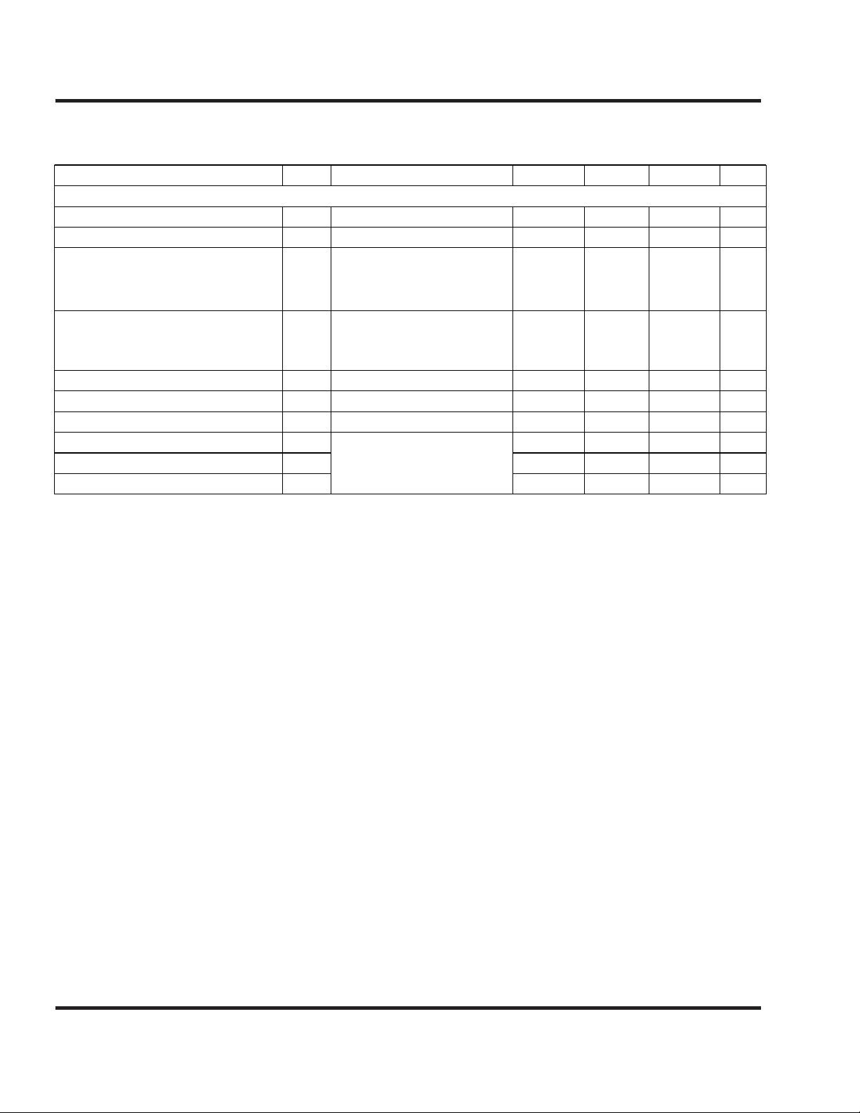
Electrical Characteristics (Contd.)
VDD = 4.75V to 5.25V, GND = 0 V, ........TA = 0oC to +70oC, MCLK = 8MHz unless otherwise stated.
PARAMETER TEST CONDITIONS MIN TYP MAX UNIT
12-Bit ADC including CDS, PGA and offset functions
Resolution VDD = 5V 12 Bits
Maximum Sampling Rate VDD = 5V 4 MSPS
Full Scale Transit ion Error Voltage at
VINP
Zero Scale Transition Error Voltage
at VINP
Differential Non Linearity DNL VDD = 5V +1.5 LSB
Number of missing codes 0 4 Code
PGA Gain
Red Channel Max. Gain, Note 1 Gr8VDD=5V 6 Times
Green Channel Max. Gain, Note 1 Gg8Mode=1 7 Times
Blue Channel Max. Gain, Note 1 Gb8 7Times
Note 1: Guaranteed monotonic up to PGA Gain code 1Fh
DAC Code = 000H, VDD=5V,
measured relative to VRT
DAC Code = 000H, VDD=5V,
measured relative to VRB
+/-50 +/-200 mV
+/-50 +/-200 mV
Wolfson Microelectronics
4
Page 5
WM8144-12
Electrical Characteristics (Contd.)
VDD = 4.75V to 5.25V, GND = 0 V, ........TA = 0oC to +70oC, MCLK = 8MHz unless otherwise stated.
PARAMETER TEST CONDITIONS MIN TYP MAX UNIT
Switching Characteristics
MCLK Period
MCLK High
MCLK Low
Data Set-up time
VSMP, RLC Da ta Hold Time
CDATA Data Hold Time
Output Propagation Delay
Output Enable TIme
Output Disable Time
Serial Interface
SCK Period
SCK High
SCK Low
SDI Set up time
SDI Hold Time
Set up time - SCK to SEN
Set up time - SEN to SCK
SEN Pulse Width
Parallel Interface
RNW Low to OP[11:4] Tristate tOPZ 20 ns
Address Setup Time to STB Low tASU 0 ns
DNA Low Setup Time to STB Low tADLS 10 ns
Strobe Low Time tSTB 50 ns
Address Hold Time from STB High tAH 10 ns
DNA Low Hold Time from STB High tADLH 10 ns
Data Set-up Time to STB Low tDSU 0 ns
DNA High Setup Time to STB Low tADHS 10 ns
Data Hold Time from STB High tDH 10 ns
DNA High Hold Time from STB High tADHH 10 ns
RNW High to OP[11:4] Output tOPD 0 ns
tPER 125 ns
tCKH
tCKL
tDSU
tDH
tDH
tPD
IOH = 1.0mA 75 ns
tPZE
tPEZ
tSPER 125
tSCKH
tSCKL
tSSU
tSCE
tSEC
tSEW
IOL = 1.0mA 75 ns
tSH
37.5 ns
37.5 ns
10
10 ns
30 ns
25 ns
37.5 ns
37.5 ns
10 ns
10 ns
20 ns
20 ns
50 ns
ns
ns
Wolfson Microelectronics
5
Page 6
WM8144-12
Pin Descriptions
Pin No. Name Type Description
23 RINP Analogue IP Red Channel input video
22 GINP Analogue IP Green Channel input video
21 BINP Analogue IP Blue Channel input video
33 CDATA[7] Digital IO Image compensation data read/write at twice ADC conversion rate
34 CDATA[6] Digital IO
35 CDATA[5] Digital IO
36 CDATA[4] Digital IO
37 CDATA[3] Digital IO
38 CDATA[2] Digital IO
39 CDATA[1] Digital IO
40 CDATA[0] Digital IO
32 MCLK Digital IP Master clock. This clock is applied at either six, four or two times the input
pixel rate depending on the operational mode. MCLK is divided internally
to define the ADC samples rate and to provide the clock source for digital
logic.
31 VSMP Digital IP Video sample synchronisation pulse. This signal is applied synchronously
with MLCK to specify the point in time that the input is sampled. The timing
of internal multiplexing between the R, G and B channels is derived from
this signal
29 RLC Digital IP Selects whether reset level clamp is applied on a pixel-by-pixel basis. If
RLC is required on each pixel then this pin can be tied high
19 V
13 V
14 V
15 V
16 V
20 V
42 OP[11] Digital IO Tri-state digital 10-bit bi-directional bus. There are four modes:
43 OP[10] Digital IO Tri-state: when OEB = 1
44 OP[9] Digital IO Output twelve-bit: twelve bit data is output from bus
45 OP[8] Digital IO Output 8-bit multiplexed: data output on OP[11:4] at 2 * ADC conversion
46 OP[7] Digital IO Input 8-bit: control data is input on bits OP[11:4]
47 OP[6] Digital IO
48 OP[5] Digital IO
1 OP[4] Digital IO
2 OP[3] Digital IO
3 OP[2] Digital IO
5 OP[1] Digital IO
6 OP[0] Digital IO
RLC
RT
RB
RU
RL
MID
Analogue OP Selectable analogue output voltage for RLC
Analogue IP ADC reference voltages. The ADC reference range is applied between
Analogue IP VRT (full scale) and VRB (zero level). VRU and VRL can be used to
Analogue IP derive optimum reference voltages from an external 5V reference
Analogue IP
Analogue OP Buffered mid-point of ADC reference string.
rate
Wolfson Microelectronics
6
Page 7
WM8144-12
Pin Descriptions (contd.)
Pin No. Name Type Description
8 CC[2] Digital OP Colour code outputs. These outputs indicate from which channel the
9 CC[1] Digital OP current output sample was taken (R = 00X, G = 01X, B = 10X).
10 CC[0] Digital OP Two codes are provided per channel.
11 ORNG Digital OP Out-of-range signal, active high. This signal indicates that the current
output pixel has exceeded the maximum or minimum achievable
somewhere within the pixel processing.
25 OEB Digital IP Output tri-state control, all outputs enabled when OEB=0
7 DV Digital OP Data valid output, active low.
12 NRESET Digital IP Reset input, active low. This signal forces a reset of all internal registers.
24 PNS Digital IP Control interface parallel (high) or serial (low, default)
27 SDI/DNA Digital IP Serial Interface: serial interface input data signal
Parallel interface: high = data, low = address
28 SCK/RNW Digital IP Serial Interface: serial interface clock signal
Parallel interface: high = OP[11:4] is output, low = OP[11:4] is input bus
26 SEN/STB Digital IP Serial Interface: enable, active high
Parallel interface: strobe, active low
30 DVDD1 Digital supply Positive Digital Supply (5V)
4 DVDD2 Digital supply Positive Digital Supply (5V)
41 DGND Digital supply Digital ground (0V)
17 AVDD Analogue supply Positive Analogue supply (5V)
18 AGND Analogue supply Analogue Ground (0V)
Wolfson Microelectronics
7
Page 8
WM8144-12
=
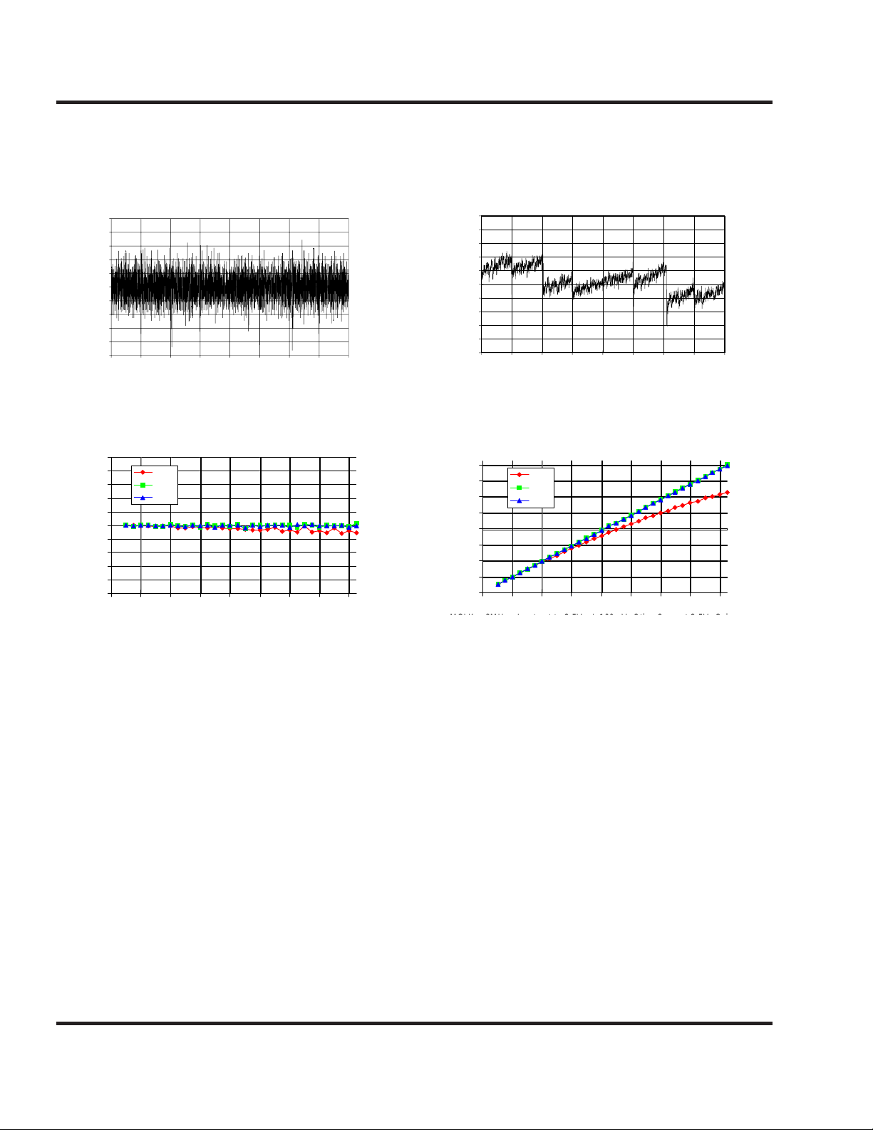
Typical Performance
VDD = 5V, GND = 0 V, ........TA = 25oC.
1
0.8
0.6
0.4
0.2
0
LSB's
-0.2
-0.4
LSB's
-0.6
-0.8
-1
0 512 1024 1536 2048 2560 3072 3584 4096
ADC Code
ADC Code
ADC 12 Bit DNL
Gain DNL
5
4
3
2
Red
Green
Blue
1
0
-1
-2
DNL
-3
-4
-5
012345678
MCLK = 8MHz. Input 2.5V +/- 100mV. Other 2 are at 2.5V. Colour. Vdd
PGA Gain Code
PGA DNL @ MCLK = 8MHz
Gain
5
4
3
2
1
0
LSB's
-1
-2
LSB's
-3
-4
-5
0 512 1024 1536 2048 2560 3072 3584 4096
ADC Code
ADC Code
ADC 12 Bit INL
PGA Gain
8
7
6
Red
Green
Blue
5
4
3
2
Actual Gain
1
0
012345678
MCLK = 8M H z . Input s et to 2.5V +/- 1 00m V . Other 2 are at 2.5V Colour.
PGA Gain Code
Gain
PGA Gain Code vs. Actual Gain
@ MCLK = 8MHz
Wolfson Microelectronics
8
Page 9
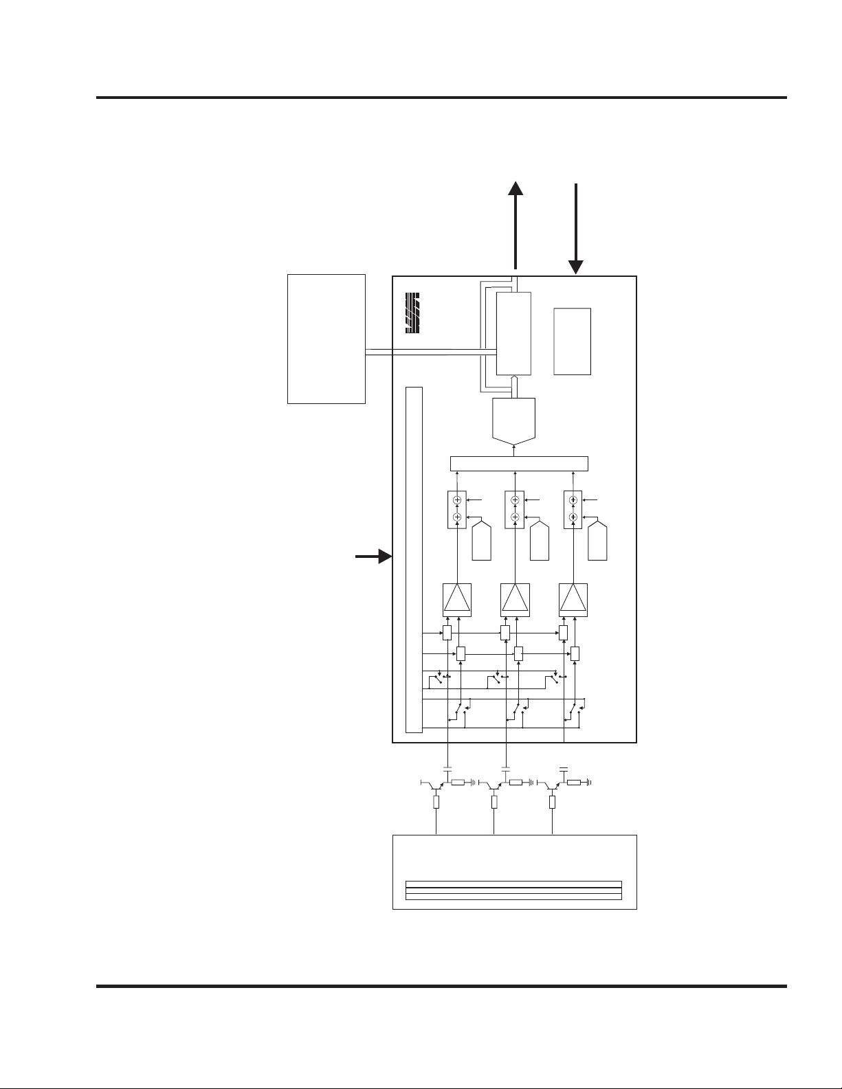
System Diagram
OPTIONAL
EXTERNAL
RAM
WM8144
TWELVE BIT IMAGE DATA
AT UPTO 4 MSPS
IMAGE
12 BIT
M
SIMPLE SERIAL OR
PARALLEL CONTROL
INTERFACE
COMPENSATION
LOGIC
ADC
X
U
CONTROL
INTERFACE
WM8144-12
SIMPLE TWO PIN
TIMING INTERFACE
MID
V
INTEGRATED TIMING CONTROL
S/H
S/H
S/H
RED
GREEN
MID
V
MID
V
OFFSET DACGAIN
AMPS
S/H
S/H
S/H
CDSCLAMP
BLUE
COLOUR
CCD
SENSOR
Wolfson Microelectronics
9
Page 10
WM8144-12
Theory of Operation
The WM8144-12 is configured to output 12-bit data by
writing to Setup Register 4: Bit 4 'Mode12'. By default
the device is configured to output 10-bit data.
S/H, Offset DAC’s and PGA
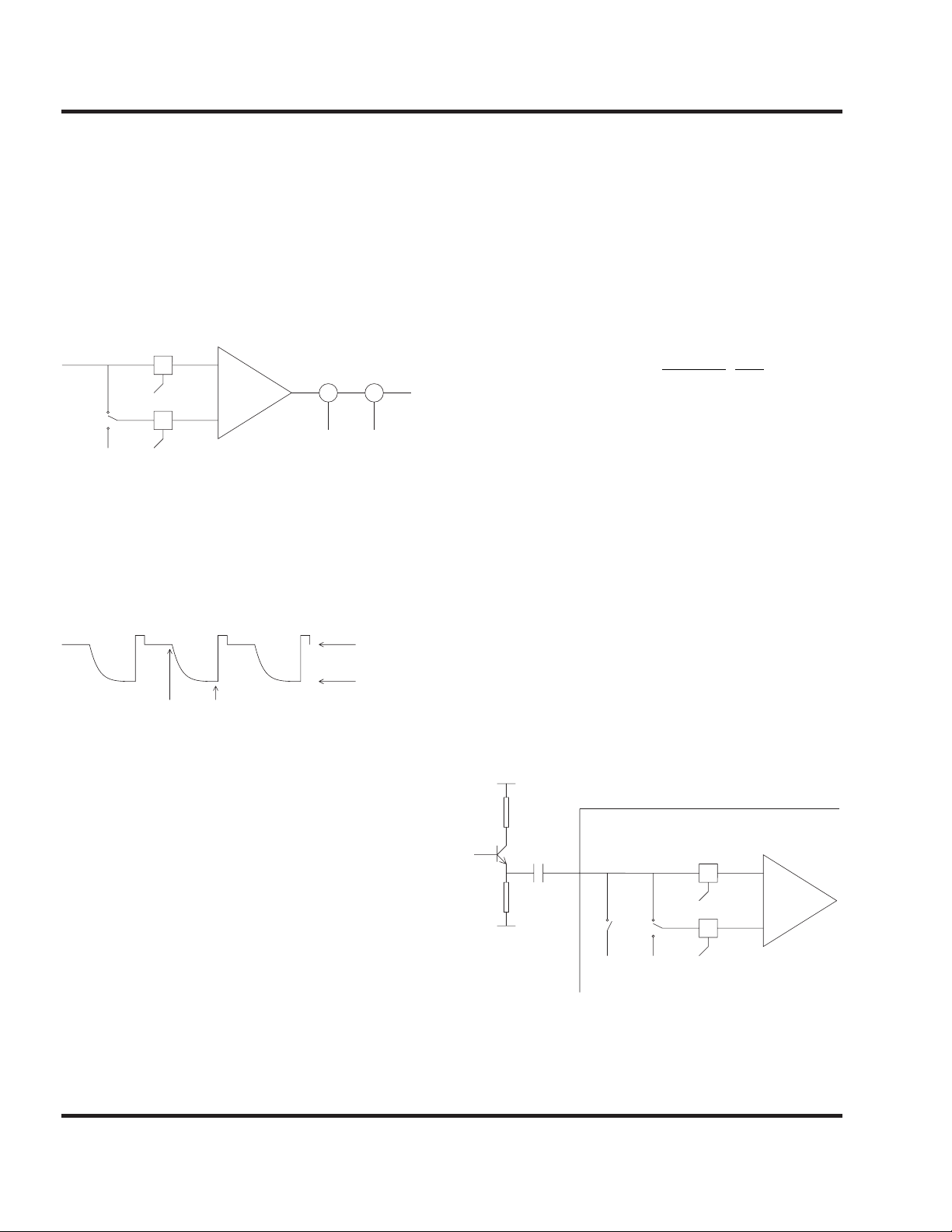
Each analogue input (RINP , GINP, BINP) of the WM814412 consists of a sample and hold, a programmable gain
amplifier, and a DC offset correction block. The operation
of the red input stage is summarised in Figure 1.
The DC value of the gained signal can then be trimmed by
the 8 bit plus sign DAC. The voltage output by this DAC is
shown as Voffset in Figure 1. The range of the DAC is
MID/2).
(V
The output from the offset DAC stage is referenced to
MID voltage. This allows the input to the ADC to
the V
maximise the dynamic range, and is shown diagrammatically in Figure 1 by the final VMID addition.
For the input stage the final analogue voltage applied to
the ADC can be expressed as:
RINP
VMID
S/H
VS
S/H
RS
+
-
Gain=G
+ +
VMIDVoffset
VADC
Figure 1
The sample/hold block can operate in two modes of operation, CDS (Correlated Double Sampling) or Single Ended.
In CDS operation the video signal processed is the difference between the voltage applied at the RINP input when
RS occurs, and the voltage at the RINP input when VS
occurs. This is summarised in Figure 2.
Vrs
Vvs
RS
VS
Figure 2
When using CDS the actual DC value of the input signal is
not important, as long as the signal extremes are maintained within 0.5 volts of the chip power supplies. This is
because the signal processed is the difference between
the two sample voltages, with the common DC voltage
being rejected.
In single ended operation, the VS and RS control signals
occur simultaneously, and the voltage applied to the reset switch is fixed at V
MID. This means that the voltage
processed is the difference between the voltage applied
to RINP when VS/RS occurs, and V
MID. When using Sin-
gle ended operation the DC content of the video signal is
not rejected.
The Programmable Gain Amplifier block multiplies the resulting input voltage by a value between 0.5 and 8.25
which can be programmed independently for each of the
three input channels via the serial (or parallel) interface.
PGA gain is dependent on the 5-bit binary code programmed in the PGA registers. A typical plot of PGA
Code versus Actual Gain is shown on Page 8.
VADC G Vvs Vrs 1 2* Sign *
=−+−
()
()
DAC_ CODE
255
VMID
2
+*
VMID
Where: VADC is the voltage applied to the ADC
G is the programmed gain
Vvs is the voltage of the video sample
Vrs is the voltage of the reset sample
Sign is the Offset DAC sign bit
DAC_CODE is the offset DAC value
MID is the WM8144-12 generated VMID voltage
V
The ADC has a lower reference of V
and an upper reference of V
RT (typically 3.5 V). When
RB (typically 1.5 V)
an ADC input voltage is applied to the ADC equal to VRB
the resulting code is 000(hex). When an ADC input voltage is applied to the ADC equal to V
RT the resulting code
is FFF(hex).
Reset Level Clamp
Both CDS and Single ended operation can be used with
Reset Level Clamping. A typical input configuration is
shown in Figure 3.
WM8144
Cin
RINP
VRLC
VMID
S/H
VS
S/H
RS
+
Gain=G
-
Figure 3
10
Wolfson Microelectronics
Page 11
Theory of Operation (contd.)
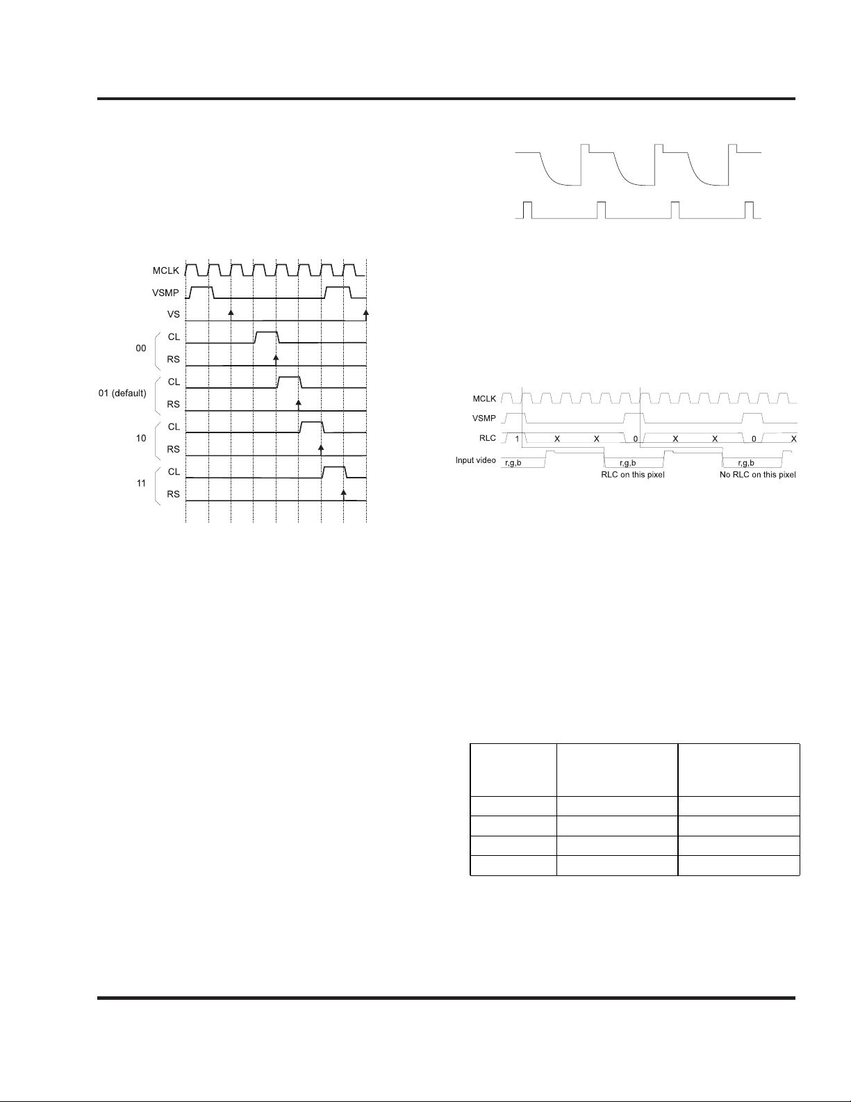
The position of the clamp relative to the video sample is
programmable by CDSREF1-0 (see T able 7). By default,
the reset sample occurs on the fourth MCLK rising edge
after VSMP. The relative timing between the reset sample ( and CL) and video sample can be altered as shown
in Figure 4.
WM8144-12
Video Input
Clamp Pulse
Figure 5
A reset level clamp is activated if the RLC pin is high on
an MCLK rising edge (Figure 6). By default this initiates
an internal clamp pulse three MCLK pulses later (Figure
4: CL). The relationship between CL and RS is fixed.
Therefore altering the RS position also alters the CL position (Figure 4). Table 7 shows the three possible
voltages to which the reset level can be clamped.
Figure 4: Reset Sample and Clamp Timing
When the clamp pulse is active the voltage on the
WM8144-12 side of Cin, i.e. RINP, will be forced to be
equal to the VRLC clamp voltage (see Figure 5). The
VRLC clamp voltage is programmable to three different
levels via the serial interface (1.5V, 2.5V or 3.5V). The
voltage to which the clamp voltage should be programmed
is dependent on the type of sampling selected and the
polarity of the input video signal. For CDS operation it is
important to match the clamp voltage to the amplitude and
polarity of the video signal. This will allow the best use of
the wide input common-mode range offered by the
WM8144-12. If the input video is positive going it is advisable to clamp to Vcl (Lower clamp voltage). If the video is
negative going it is advisable to clamp to Vcu (Upper
clamp voltage). Regardless of where the video is clamped
the offset DAC is programmed to move the ADC output
corresponding to the reset level to an appropriate value
to maximise the ADC dynamic range. For Single Ended
operation it is recommended that the clamp voltage is set
to Vcm (Middle clamp voltage).
Figure 6: RLC Timing
RINP, GINP and BINP Input Impedence
The input impedence of the WM8144-12 analogue inputs
is dependent on the sampling frequency of the input signal and the configuration of the internal gain amplifiers.
The input impedence = 1/(Capacitance * frequency)
where the Capacitance value changes from 0.3pF for
minimum gain to 9.6pF for maximum gain. Table 1 illustrates the minimum and maximum input impedence at different frequencies.
Sampling
Frequency
(MHz)
0.5 6.6 208
13.3 104
21.6 52
40.8 26
Table 1: Effects of Frequency on Input Impedence
Impedence with
minimum gain
(MΩ)
Impedence with
maximum gain
(KΩ)
Wolfson Microelectronics
11
Page 12

WM8144-12
Theory of Operation (Contd)
Example of Gain and Offset Operation
Input Video polarity negative
Input sampling CD S
Input voltage amplitude (V
Programmable gain x1
Clamping Y es, V
After the input capacitor the input to the WM8144-12 can
be represented as:
RS
VS - VRS) 1.6V
CL = 3.5V
Vrs
Vvs
VS
For a white pixel: V
RS = VCL
VVS = VCL - 1.6
For the white pixel, using the same offset DAC value, the
ADC input can be expressed as:
164 V
V = 1*(V - 1.6 - V ) + (1 - 2*0) * * + V
ADC CL CL MID
V = -1.6 + * V + V
ADC MID MID
V = * V - 1.6
ADC MID
82
255
337
255
MID
255 2
Figure 7
For a black pixel: V
RS = VCL
VVS = VCL
Assuming that the offset DAC is set to 00dec:
VADC = 1* Vcl - Vcl
VADC 0+ 0 +VMID
VADC = VMID
()
=
120
** *VMID
+−
()
255 2
0
VMID
+
VMID
An input voltage of VMID corresponds to a code of
2048(dec) from the ADC.
To maximise the dynamic range of the ADC input it is
necessary to program the offset DAC code to move the
ADC code corresponding to the black level towards code
4096(dec).
Hence set the offset DAC to 164(dec) with the sign bit
not set.
164 V
V = 1*(V - V ) + (1 - 2*0) * * + V
ADC CL CL MID
V = 0 + * V + V
ADC MID MID
82
255
MID
255 2
When the VMID is 2.5V, the ADC input voltage becomes
1.7 volts which will result in a code of 409(dec). This is
near the ideal full-scale of 000(dec).
Therefore the output codes from the ADC are between
3686(dec) and 409(dec), which implies that the ADC
input has been set up to maximise the dynamic range
available. If a digital representation of the ADC output
with a black level near 000(dec) and a white level near
4095(dec) is required then the INVOP control bit should
now be set to ONE.
V = * V
337
ADC MID
255
When the VMID is 2.5v, the ADC input voltage becomes
3.3 volts which will result in an ADC code of 3686(dec).
This is near the ideal full-scale of 4095(dec).
Wolfson Microelectronics
12
Page 13
Theory of Operation (contd.)
WM8144-12
CDATA
DEFAULT
ADCOP
Figure 8
DEMUX
AND MUX
612
MUX MUX
12 13
PIXEL OFFSET
ADDER
4,5 or 6
Figure 12
DATA
PARTITIONING
LIMIT
DEFAULT
12,11 or 10
12
MUX
MUX
PIXEL GAIN
ADJUST
Digital Signal Processing
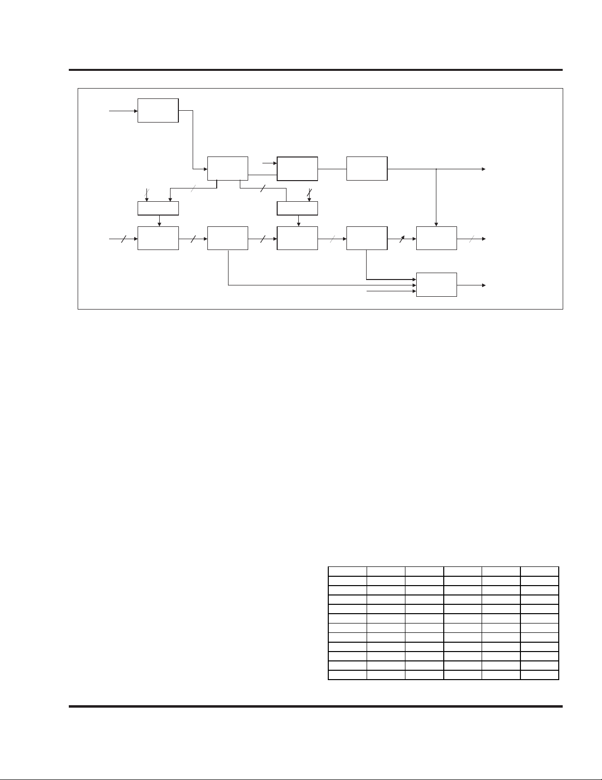
By default, the output from the ADC passes through the
digital compensation block without being altered and is
output directly on the OP[11:0] pins. If required, the pixel
data from the ADC can be processed further by the
digital compensation block (Figure 8). This section describes the sub-blocks of the digital compensation block.
CDATA Demultiplexor
The input to this block is coefficient data presented to the
CDATA[7:0] pins at twice the pixel rate. i.e. two eight-bit
words are input for each pixel of video data.
Data Partitioning
The sixteen bits of data per pixel from the CDATA
Demultiplexor is partitioned into pixel offset, pixel gain
and pixel valid bits (Table 3). Table 4 details the resulting
range and resolution options.
Pixel Offset Adder
This uses the offset coefficients that are either supplied
externally via the CDATA interface or from the internal
default registers. The object of this block is to correct for
the small offsets which can occur from the CCD on a
pixel-by-pixel basis. The output from the Pixel Offset
Adder is limited to be between 0 and 4095(dec).
Pixel Gain Adjust
This block corrects for the pixel-by-pixel shading curve
non-uniformity and photo response non-uniformity within
the CCD sensor. This block has a gain range of 0 to 2.
The output word from the Pixel Gain Adjust is limited to
between 0 and 4095(dec).
DATA VALID
GENERATION
DEFAULT
24 12 12
ADC
LIMIT
DATA
LATCH
OUT OF RANGE
GENERATION
DV OUTPUT
OP[11:0] INPUT TO
12/8 MUX BLOCK
ORNG INPUT TO
12/8 MUX BLOCK
Effect of digital compensation on ADC output
The combined effect of the digital compensation sections on the ADC output is summarised by the formula:
OP[11:0] = (ADCOP + POC) * PSCF
where:
All values are decimal
OP[11:0] is the 12 bit result output from the WM8144-12
ADCOP is a 12 bit unsigned number from the ADC
POC is a 2's compliment number divided byNUMBER OF
POC BITS ALLOCA TED incrementing in steps of four (e.g.
-32,-28,-24.....24,28)
PSCF is an unsigned number divided by NUMBER OF PSC
BITS ALLOCA TED/2
For this example assume PSC is allocated 12 bits and
POC is allocated 4 bits (refer to table
3:DVMODE,PWP0,PWP1 = 0). Table 2 shows some examples of the effect of the digital backend on the ADC
output.
Range 0:4095 -32:28 0:4095 0:4095 0:1
Default 0 2048 (x1)
Ex 1 2048 0 2048 204 8 0
Ex 2 2048 -32 2048 2016 0
Ex 3 2048 8 2048 205 6 0
Ex 4 4091 8 2048 409 5 1
Ex 5 4091 8 512 1023 1
Ex 6 2048 0 2560 256 0 0
Ex 7 2048 0 512 512 0
Ex 8 2049 0 4095 409 5 1
Ex 9 2048 0 4095 409 5 0
ADCOP POC PS C OP[11: 0] ORN G
Table 2: Examples of digital backend calculation
Wolfson Microelectronics
13
Page 14
WM8144-12
ps)
Theory of Operation (contd.)
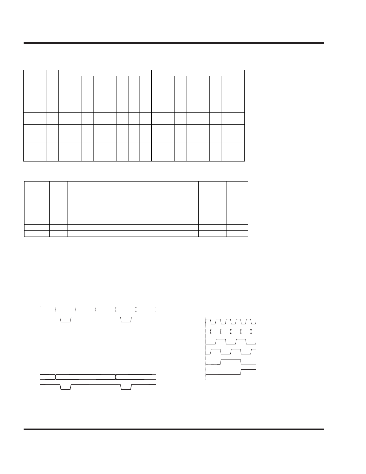
CDATA WORD 1 CDATA WORD 2
D
P
P
B7 B6 B5 B4 B3 B2 B1 B0 B7 B6 B5 B4 B3 B2 B1 B0
V
W
W
M
P
P
O
1
0
D
E
0 0 0 G11G10G9G8G7G6G5G4G3G2G1G0O3O2O1O0
0 0 1 G10 G9 G8 G7 G6 G5 G4 G3 G2 G1 G0 O4 O3 O2 O1 O0
0 1 0 G9G8G7G6G5G4G3G2G1G0O5O4O3O2O1O0
1 0 0 G10 G9 G8 G7 G6 G5 G4 G3 G2 G1 G0 DV O3 O2 O1 O0
1 0 1 G9G8G7G6G5G4G3G2G1G0DVO4O3O2O1O0
Table 3: Bit Allocation Assignment
DVMODE PWP1 PWP0 No. of
offset
0 0 0 4 -32 : 28 12 0:2 1 0
0 0 1 5 -64 : 56 11 0:2 2 0
0 1 0 6 -128 : 112 10 0:2 4 0
1 0 0 4 -32 : 28 11 0:2 2 1
1 0 1 5 -64 : 56 10 0:2 4 1
offset range No. of gain
bits
bits
gain
range
resolution
Table 4: Bit Range and Resolution Options
Data Valid Generation
The DV pin can be controlled to determine whether a DV
pulse will be generated for a particular pixel. For example, if red pixels only are required the following DV pulse
can be generated.
Output data interface
Typically, data is output from the device as a twelve-bit
wide word on OP[11:0] - assuming the MODE12 bit is
set. Optionally, data can be output in an eight-bit word
format. Figure 1 1 shows this function. Data is presented
on pins OP[11:4] at twice pixel rate.
OP[11:0]
DV
BBG GRR
MCLK
Figure 9
OP[11:4]
Data Latch
Under control of the LATCHOP bit the output data bus
can be prevented from clamping until the next Data V alid
pulse. Hence the above output would become:
OP[11:0]
DV
RR
Figure 10
DV
CC[0]
CC[1]
CC[2]
A = d11,d10,d9,d8,d7,d6,d5,d4
B = d3,d2,d1,d0,X,X,X,ORNG
gain
(LSB
ste
DV bits
A
B
Figure 11: Eight-bit Multiplexed Bus
Output
Wolfson Microelectronics
14
Page 15

Operating Modes
Video Sampling Options
WM8144-12 can interface to CCD sensors using four
basic modes of operation ( summarised in Table 5). Mode
configurations are controlled by a combination of control
bits and timing applied to MCLK and VMSP pins. The default operational mode is mode 1: colour with CDS enabled.
Colour mode definition (mode 1)
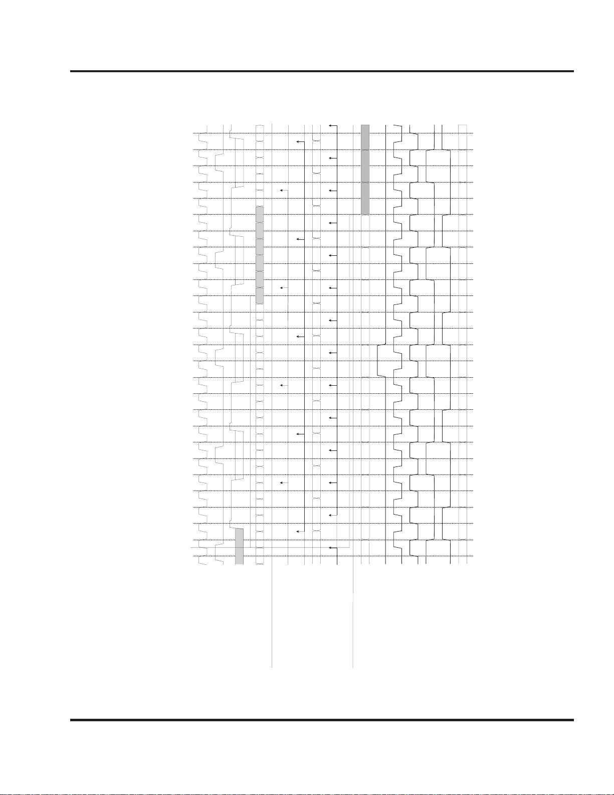
Figure 12 summarises the timing relationships within the
Colour mode. MCLK is applied at twice the required ADC
conversion rate. Synchronisation of sampling and channel multiplexing to the incoming video signal is performed
by the VSMP pulse (active high). The three input channels (R,G,B) are sampled in parallel on the rising edge of
MCLK following a VSMP pulse. The sampled data is multiplexed into a single data stream at three times the VSMP
rate and passes through the internal pipeline and emerges
on the OP[11:0] bus 20.5 MCLK periods later.
If the digital post-processing stage is activated, compensation data will be clocked into the device at twice the
ADC conversion rate (e.g. two reads per red pixel ). The
first of the two bytes will be required on the CDATA bus
15.5 MCLK periods after the corresponding VSMP pulse.
CC[2:0] can be used to control the three lower address
lines of an external RAM. Both Correlated Double Sampling (CDS) and Single Ended modes of operation are
available.
WM8144-12
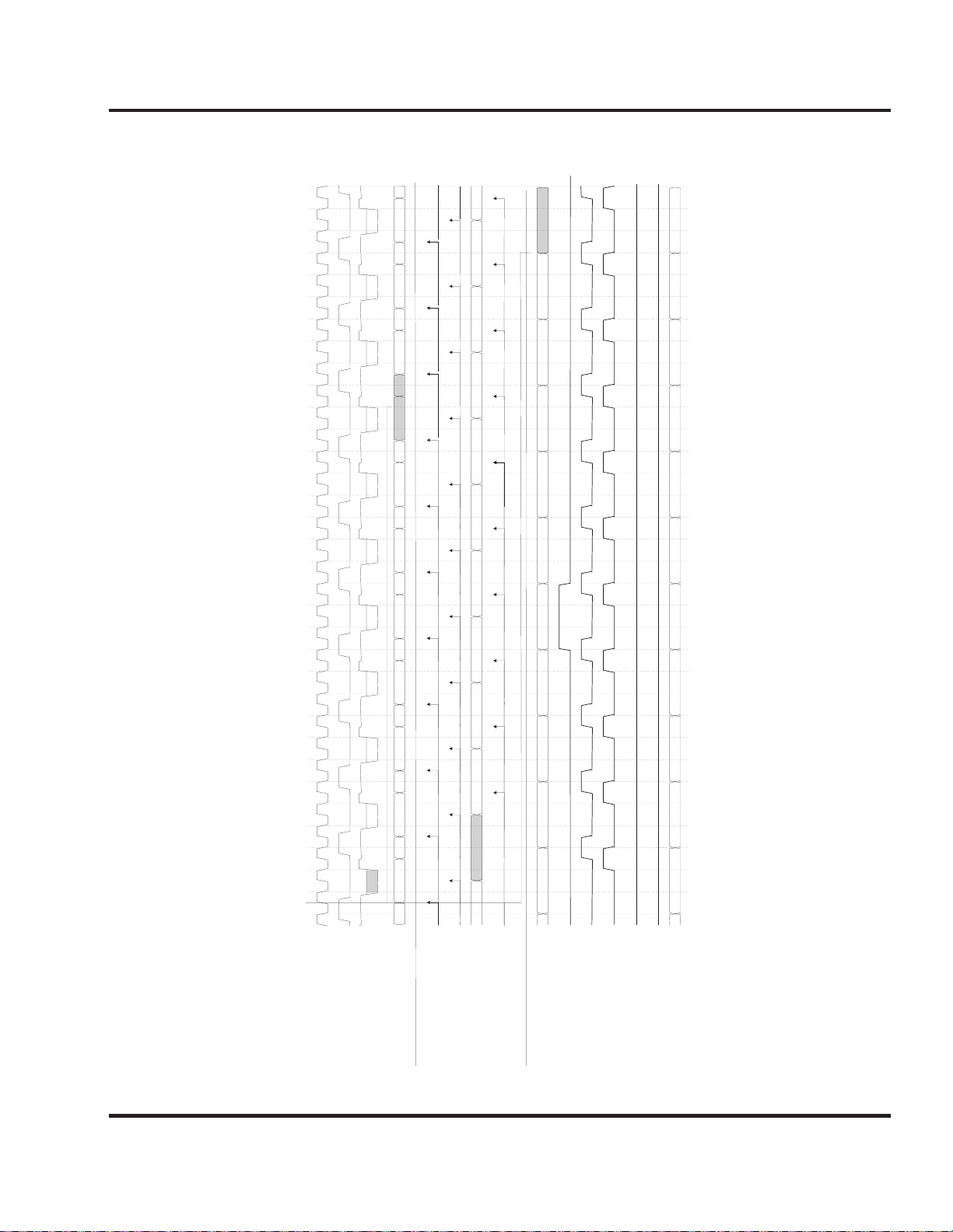
to 3:1. In this mode, the timing of RS and CL must be
fixed (refer to Table 5).
The sampled video data will pass through the internal
pipeline and emerge on the OP[11:0] bus 29.5 MCLK
periods later.
If the digital post-processing stage is activated compensation data will be clocked into the device at twice
the internal pixel rate (e.g. two reads per red pixel ).
The first of the two bytes will be required on the CDA TA
bus 22.5 MCLK periods after the corresponding VSMP
pulse.
Details of Max. Speed Monochrome mode
(mode 4)
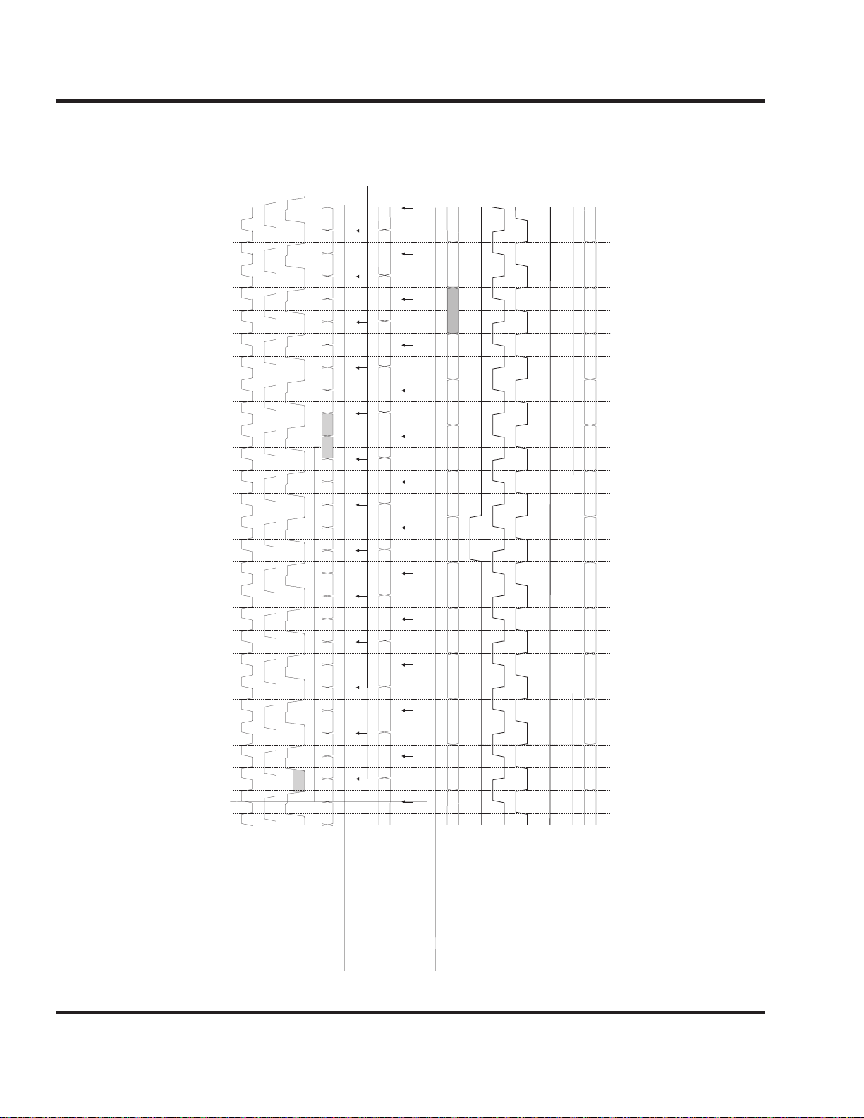
Figure 15 summarises the timing relationships. This
mode allows the maximum sample rate to be increased
to 4 MSPS. This is achieved by altering the MCLK:VSMP
ratio to 2:1. The latency through the device is identical
to modes 1 and 2. CDS is not available in this mode.
Monochrome mode definitions
One input channel is continuously sampled on the rising
edge of MCLK following a VSMP pulse. The user can
specify which input channel (R,G,B) to be sampled by
writing to WM8144-12 internal control registers. There
are three separate monochrome modes with different
maximum sample rates and CDS availability .
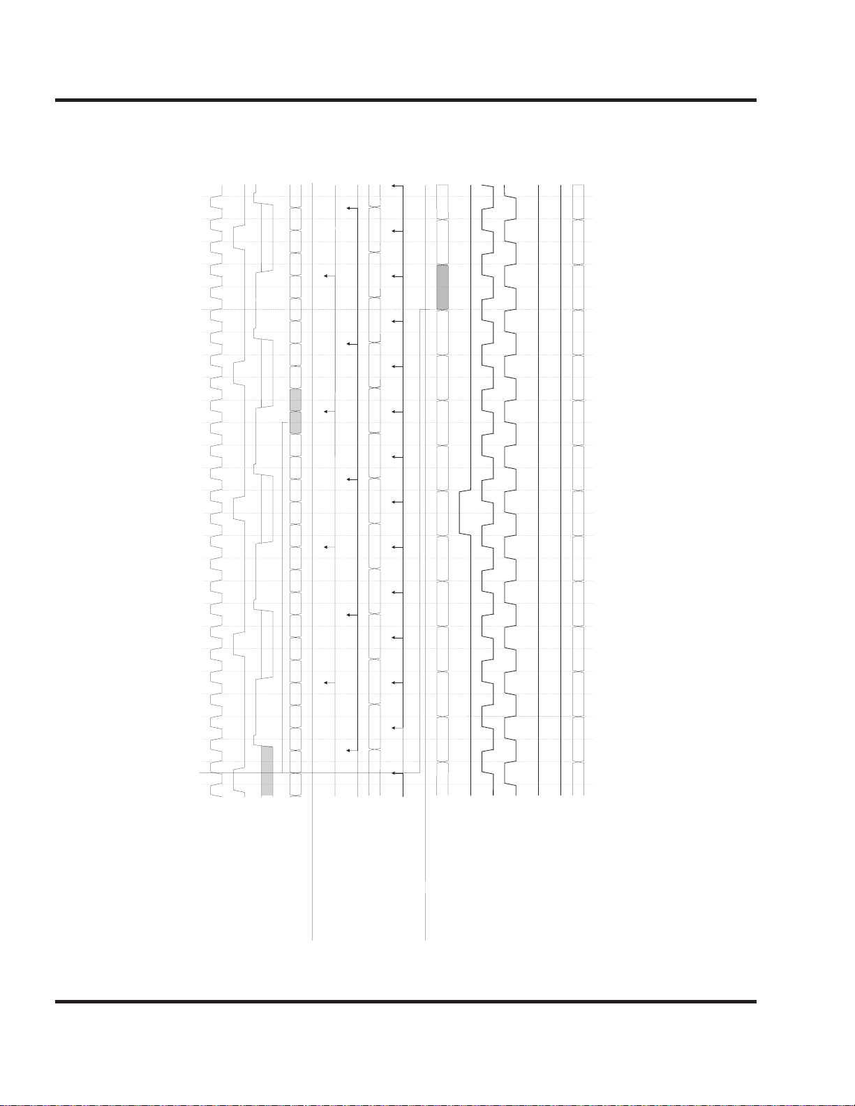
Details of Monochrome mode timing (mode 2)
Figure 13 summarises the timing relationships. The timing
in this mode is identical to mode 1 except for the CC[2:0]
outputs. One input channel is sampled three times ( due
to the multiplexer being held in one position) and passes
through the device as three separate samples. Two of
the samples can be ignored at the output. The CC[2:1]
output pins reflect the input channel selected (R,G or B).
Details of Fast Monochrome mode timing
(mode 3)
Figure 14 summarises the timing relationships. This mode
allows the maximum sample rate to be increased to 2.66
MSPS. This is achieved by altering the MCLK:VSMP ratio
Wolfson Microelectronics
15
Page 16

16
Table 5: WM8144-12 Mode Summary
Theory of Operation (contd.)
WM8144-12
Mode Description CDS
1 Colour Yes 1.33
Wolfson Microelectronics
2 Monochrome Yes 1.33
3Fast
Monochrome
4 Max Speed
Monochrome
* Only indicates relevant register bits
Max.
available
Yes 2.66
No 4 MSPS Identical t o Mode 2 MCLK max. 8MHz.
Sample
Rate
MSPS
MSPS
MSPS
Sensor Interface
Description
The three input
channels (R,G,B) are
sampled in parallel at
max. 2MSPS. The
sampled data is
multiplexed into a
single data s tream
before the internal
ADC giving an
internal s erial data
rate of max. 4MSPS.
One input channel is
continuousl y
sampled. The internal
multiplexer is held in
one position under
control of the user.
Identical to Mode 2 MCLK m ax. 8MHz.
Timing Requirem ents Register Contents
MCLK max. 8MHz.
MCLK:VSMP ratio is 6:1.
Identical to Mode 1 Setup Reg 1: 1F(H)
MCLK:VSMP ratio is 3:1.
MCLK:VSMP ratio is 2:1.
Register Contents
with CDS*
Setup Reg 1: 1B(H) Set up Reg 1: 19(H)
Setup Reg 3: bits
b[7-6] define which
channel to be
sampled
Identical to Mode 2
plus Setup Reg 3: bits
b[5-4] must be set to
00(H)
Not Applicable Setup Reg 1: 5D(H)
without CDS*
Setup Reg 1: 1D(H)
Setup Reg 3: bit s b[76] define which
channel to be
sampled
Identical to Mode 2
Setup Reg 3: bit s b[76] define which
channel to be
sampled
Page 17
WM8144-12
Operating Modes (contd.)
r1:1 r1:2 g1:1 g1:2 b1:1 b1:2
Device timing for mode 1
b1
g1
r1
b2 b3 r4 g4 b4
2
1111
0000 22221
MCLK
VSMP
INPUT
SIGNALS
r2,g2,b2 r3,g3,b3 r4,g4,b4 r5,g5,b5
r1,g1,b1
Input video
2345
2345
15.5 MCLK periods
1
RS
CDATA[7:0]
g2r2 g3r3b1
b0 g1r1
VS
ADC input
INTERNAL
SIGNALS
20.5 MCLK periods
OP[11:0]
ADC sample
ORNG
OUTPUT
DV
CC[0]
SIGNALS
CC[1]
CC[2]
CC[2:1]
Figure 12: Default Timing in CDS Colour Mode
Wolfson Microelectronics
17
Page 18
WM8144-12
Operating Modes (contd.)
Device timing for mode 2
XXXXX XXXXX
r1
r1:1 r1:2 X XXXXXXXXX XXXXX XXXX
2345
r2,g2,b2 r3,g3,b3 r4,g4,b4 r5,g5,b5
XXXXr1 XX XXX
20.5 MCLK periods
1
VS
ADC input
INTERNAL
SIGNALS
ADC sample
OP[11:0]*
ORNG
OUTPUT
DV
CC[0]
SIGNALS
CC[1]*
MCLK
VSMP
INPUT
SIGNALS
r1,g1,b1
Input video
2345
15.5 MCLK periods
RS
CDAT A[7:0]
Figure 13: Default Timing in CDS Monochrome Mode
CC[2]*
00000000000000
'X' indicates don't care
* This example shows function when Red channel selected. CC[1] and CC[2] indicate the selected channel (R,G or B)
CC[2:1]
18
Wolfson Microelectronics
Page 19
WM8144-12
Operating Modes (contd.)
Device timing for mode 3
n
n:2
n:1
00 000000000
* This example shows function when Red channel selected. CC[1] and CC[2] indicate the selected channel (R,G or B)
CC[1]*
CC[2]*
CC[2:1]*
MCLK
VSMP
INPUT
SIGNALS
n+1
n
Input video
22.5 MCLK periods
RS
CDATA[7:0]
n
VS
ADC input
INTERNAL
SIGNALS
29.5 MCLK periods
OP[11:0]
ADC sample
ORNG
OUTPUT
DV
CC[0]
SIGNALS
Figure 14: Default Timing in Fast CDS Monochrome Mode
Wolfson Microelectronics
19
Page 20
WM8144-12
Operating Modes (contd.)
n:1 n:2
Device timing for mode 4
00
n
0
00
0
MCLK
n
VSMP
Input video
15.5 MCLK periods
1
VS
CDATA[7:0]
n
ADC input
ADC sample
20.5 MCLK periods
ORNG
OP[11:0]
DV
CC[0]
CC[1]*
00
0
000
00
* This example shows function when Red channel selected. CC[1] and CC[2] indicate the selectedc channel (R,G or B)
CC[2]*
CC[2:1]*
20
INPUT
SIGNALS
INTERNAL
SIGNALS
OUTPUT
SIGNALS
Figure 15: Default Timing in Max. Speed non-CDS Monochrome Mode
Wolfson Microelectronics
Page 21
Configuration of the WM8144-12
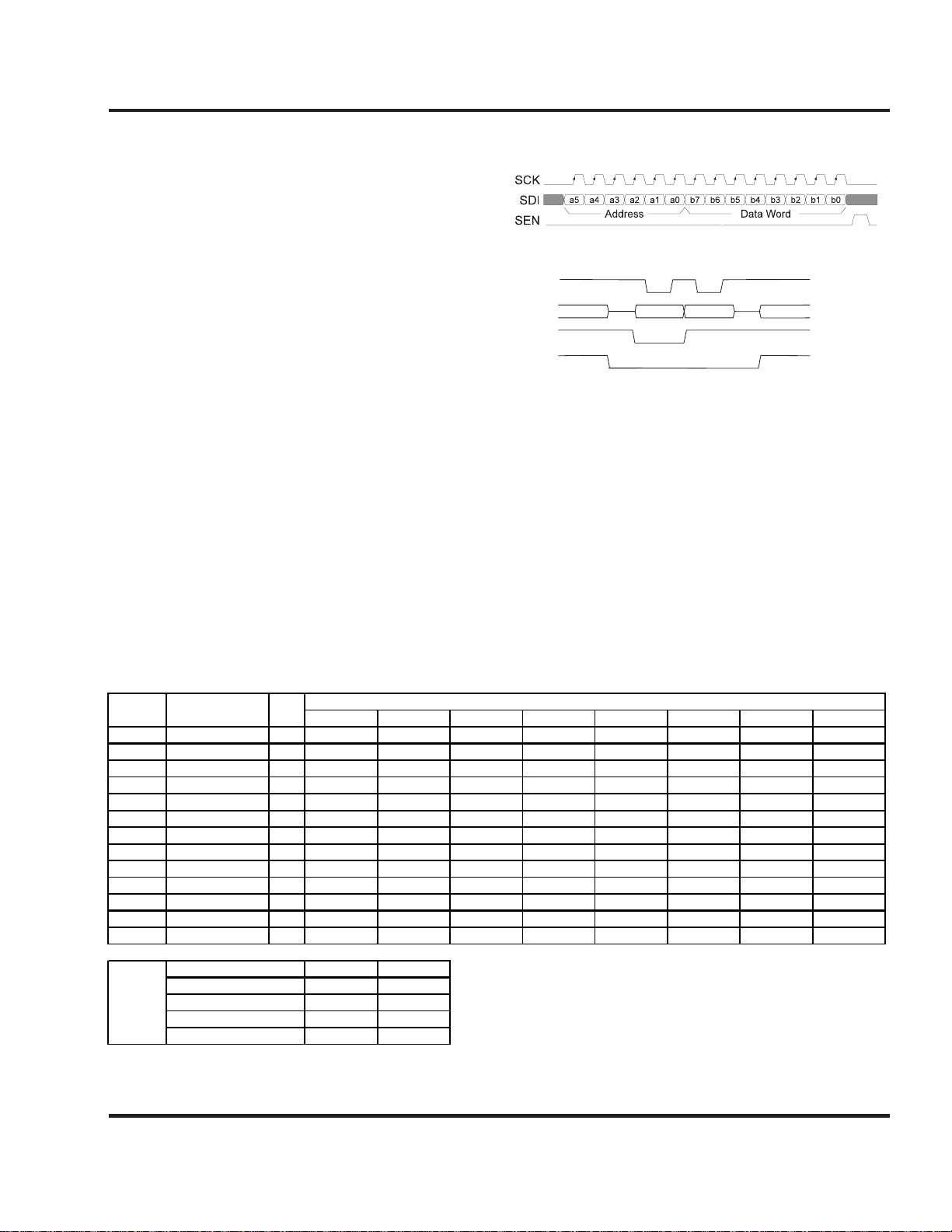
The WM8144-12 can be configured through a serial
interface or a parallel interface. Selection of the
interface type is by the PNS pin which must be tied
high (parallel) or low (serial).
Serial Interface
The serial interface consists of three pins (refer to
figure 16 ). A six-bit address is clocked in MSB first
followed by an eight-bit data word, also MSB first.
Each bit is latched on the rising edge of SCK, which
can operate at up to 8MHz. Once the data has been
shifted into the device, a pulse is applied to SEN to
transfer the data to the appropriate internal register.
Parallel Interface
The parallel interface uses bits [11:4] of the OP bus as
well as the STB, DNA and RNW pins (refer to figure
17). Pin RNW must be low during a write operation.
The DNA pin defines whether the data byte is address
(low) or data (high). The data bus OP[11:4] is latched in
during the low period of STB. This interface is
compatible with the Extended Parallel Port interface.
Internal Register Definition
Table 6 summarises the internal register content. The
first 4 addresses in the table are used to program setup
registers and to provide a software reset feature ( 00H
is reserved ). The remaining 7 entries in the table define
WM8144-12
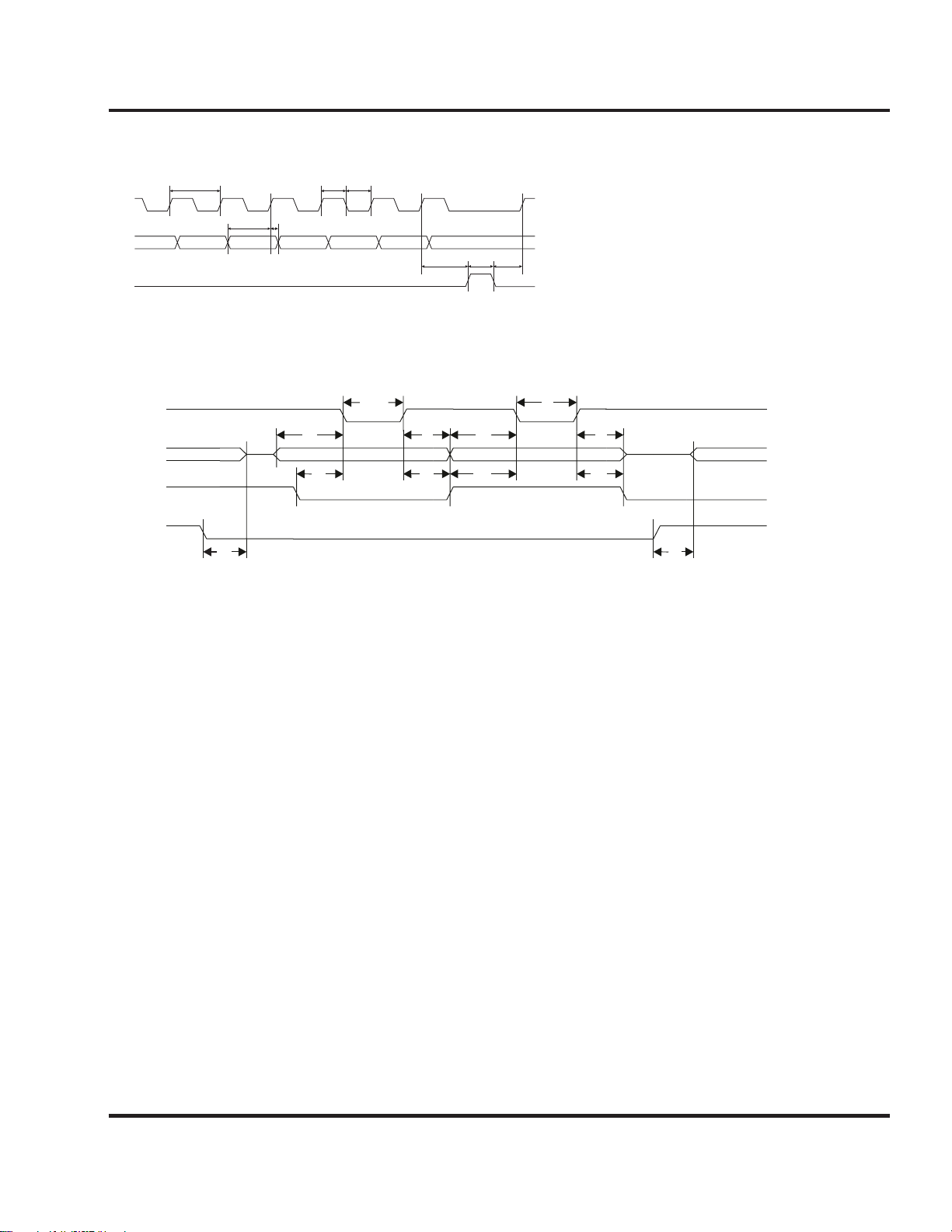
Figure 16: Serial Interface Timing
STB
OP[11:4]
DNA
RNW
Address
Figure 17: Parallel Interface Timing
the address location of internal data registers. In each
case, a further three sub-addresses are defined for the
red, green and blue register. Selection between the red,
green and blue registers is performed by address bits a1
and a0, as defined in the table. Setting both a1 and a0
equal to 1 forces all three registers to be updated to the
same data value. Blank entries can be taken as 'don't care'
values.
Data
Address Description Def'lt
<a5:a0> (Hex) b7 b6 b5 b4 b3 b2 b1 b0
000000 Reserved
000001 Setup Register 1 1B DVMODE VSMP4M DEFDV DEFPO DEFPG MONO CDS ENADC
000010 Setup Register 2 00 CDATOUT BYPASS LATCHOP INVOP MUXOP
000011 Setup Register 3 11 CHAN[1] CHAN[0] CDSREF[1] CDSREF[0] PWP[1] PWP[0] RLC[1] RLC[0]
000100 Software Reset 00
000101 Setup Register 4 00 MODE12 DACRNG
1000xx DAC values 00 DAC[7] DAC[6] DAC[5] DAC[4] DAC[3] DAC[2] DAC[1] DAC[0]
1001xx DAC signs 00 DSIGN
1010xx PGA Gains 00 PGA[4] PGA[3] PGA[2] PGA[1] PGA[0]
1011xx Pixel Offsets 00 OFF[5] OFF[4] OFF[3] OFF[2] OFF[1] OFF[0]
1100xx Pixel Gain MSB 80 GAIN[11] GAIN[10] GAIN[9] GAIN[8] GAIN[7] GAIN[6] GAIN[5] GAIN[4]
1101xx Pixel Gain LSB 00 GAIN[3] GAIN[2] GAIN[1] GAIN[0]
1110xx Data Valid 01 DV
xx
Address LSB decode a1 a0
Red Register 0 0
Green Register 0 1
Blue Register 1 0
Red, Green and Blue 1 1
Bit
Table 6: Register Map Contents
Wolfson Microelectronics
21
Page 22
WM8144-12
Configuration of the WM8144-12 (Contd.)
Register Bi t Bit(s) Default Description
Setup 0 ENADC 1 ADC standby control: 0 = standby, 1 = active
Register 1 1 CDS 1 Select Correlated double sampling mode: 0 = normal sampling, 1 =
CDS mode
2 MONO 0 Mono/Colour select: 0 = colour, 1 = monochrome operation
3 DEFPG 1 Select Default Pixel Gain: 0 = external pixel gain, 1 = internal
4 DEFPO 1 Select Default Pixel Offsets: 0 = external pixel offsets, 1 = internal
5 DEFDV 0 Select default internal Data Valid: 0 = external DV, 1 = internal
6 VSMP4M 0 Required when in mode 4: 0 = other mode, 1 = mode 4
7 DVMODE 0 External Data Valid control (refer to Bit Allocation Assignment table)
Setup 0 MUXOP 0 Eight bit output mode: 0 = twelve-bit, 1 = 8-bit multiplexed
Register 2 1
2 INVOP 0 Inverts ADC output: 0 = non-inverting, 1 = inverting
3 LATCHOP 0 OP bus updated on DV pulse; OP bus updated each sample, 1 = update
only on DV pulse
4 BYPASS 0 Bypass digital post-processing; 0 = no bypass, 1 = bypass
5 CDATOUT 0 Data on OP pins available on CDAT pins; 0 = no, 1 = yes
6
7
Setup 1-0 RLC1-0 01 Reset Level Clamp voltage
Register 3 00 = 1.5V
01 = 2.5V
10 = 3.5V
11 = Reserved
3-2 PWP1-0 00 Par allel Word Partitioning
See Bit Allocation Assignment (Table 3)
5-4 CDSREF1-0 01 CDS Mode Reset Timing Adjust
00 = Advance 1 MCLK Period
01 = Normal
10 = Retard 1 MCLK Period
11 = Retard 2 MCLK Period
7-6 CHAN1-0 00 Monochrome mode channel select
00 = Red Channel
01 = Green Channel
10 = Blue Channel
11 = Reserved
Setup
Register 4
1 DACRNG 0 Alters range of of fset DAC outp u t
0 = DAC output range equal to Vmid/2 (1.25V)
1= DAC output range equal to 1.5 *Vmid/2 (1.875V)
4 MODE12 0 Enable 12-bit ADC output: 0 = ten-bit, 1 = twelve-bit
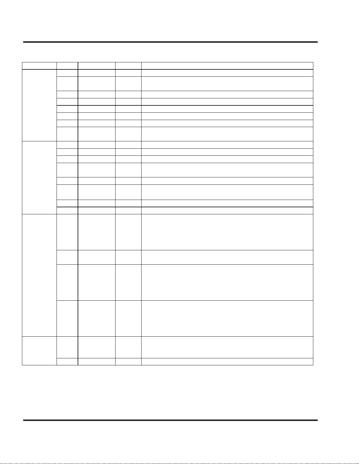
Table 7: Control Bit Descriptions
22
Wolfson Microelectronics
Page 23
Detailed timing diagramsDetailed timing diagrams
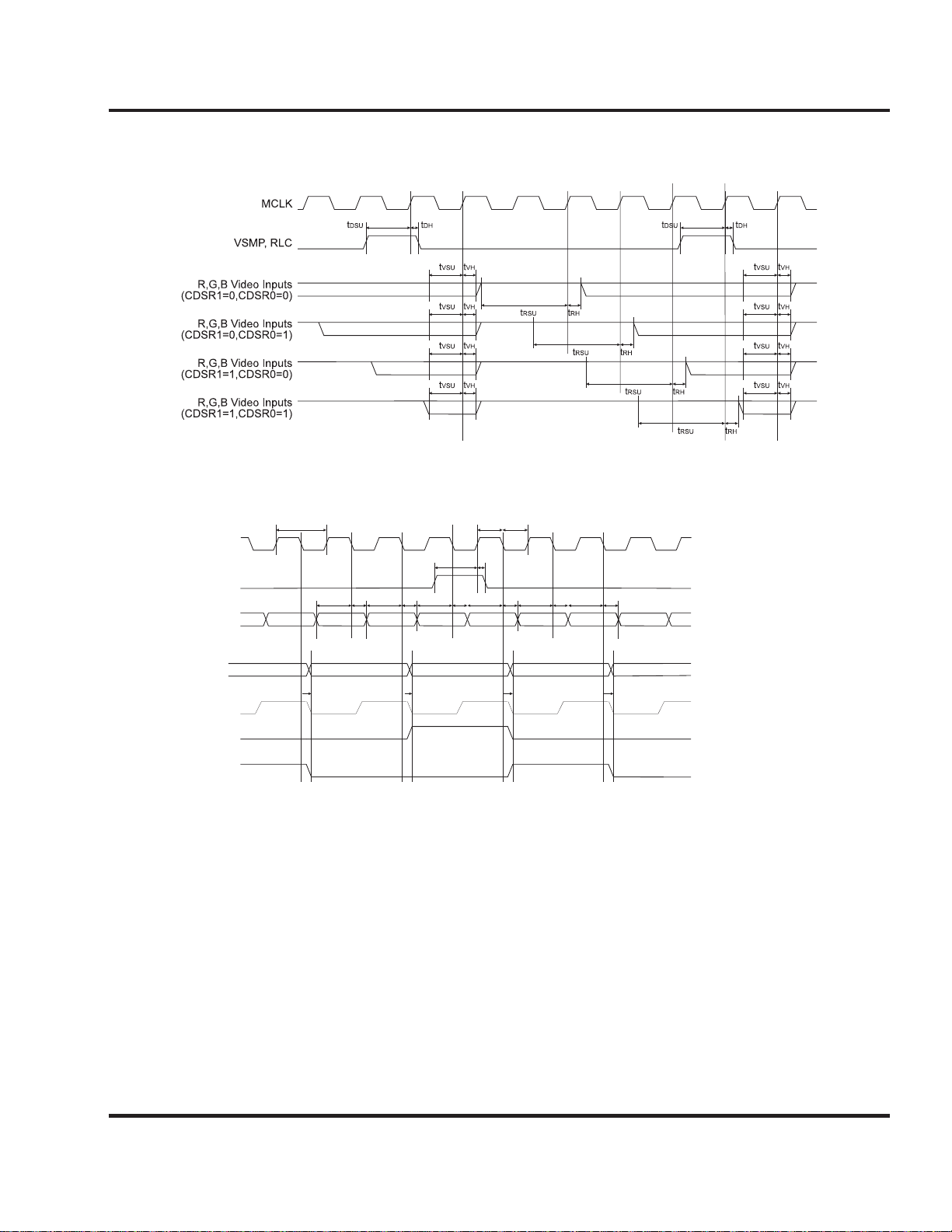
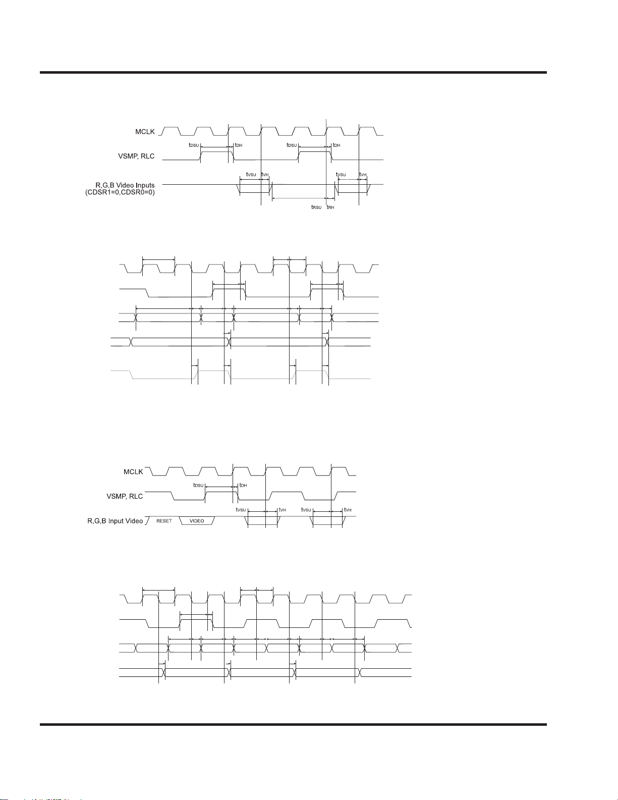
Figure 18: Detailed Video Input Timing - Modes 1 and 2
t
CKHtCKL
t
DH
t
DSU
t
DH
t
MCLK
VSMP, RLC
CDATA[7:0]
t
PER
t
DSU
t
t
DSU
RED 1 GREEN 1 BLUE 1RED 2 GREEN 2 BLUE 2
DSU
t
DH
t
DSU
t
DH
WM8144-12
t
t
DSU
DH
DSU
t
t
DH
DH
OP[11:0]
t
PD
RED GREEN BLUE
t
PD
CC[0]
CC[1]
CC[2]
Figure 19: Detailed Digital Timing - Modes 1 and 2
t
PD
t
PD
Wolfson Microelectronics
23
Page 24
WM8144-12
Detailed timing Diagrams (Contd.)
Detailed timing Diagrams (Contd.)
Figure 20: Detailed Video Input Timing - Mode 3
t
PER
MCLK
t
VSMP, RLC
CDATA[7:0]
OP[11:0]
DSU
t
DSU
WORD 1 WORD 1WORD 2 WORD 2
t
DSU
t
DH
t
t
DH
t
DH
PD
t
CKHtCKL
t
DSU
t
DSU
t
DSU
t
DH
t
DH
t
DH
t
PD
t
t
PD
PD
CC[0]
Figure 21: Detailed Digital Timing - Mode 3
Figure 22: Detailed Video Input Timing - Mode 4
t
CKHtCKL
t
DSU
t
DH
t
PD
t
DH
MCLK
VSMP, RLC
CDATA[7:0]
OP[11:0]
t
PER
t
DSU
t
DSU
1212
t
PD
t
DH
t
DSU
t
DH
t
t
PD
t
DSU
t
PD
PD
t
t
DSU
t
DH
DSU
t
t
DH
DH
Figure 23: Detailed Digital Timing - Mode 4
Wolfson Microelectronics
24
Page 25
Detailed timing Diagrams (Contd.)
t
t
SPER
SCK
t
SSU
SDI
SEN
Figure 24: Detailed Timing Diagram for Serial Interface
STB
OP[11:4]
DNA
RNW
8144 Out
t
Z
OPZ
SCKHtSCKL
t
SH
t
SCEtSEWtSEC
t
STB
t
ASU
t
AH
t
DSU
Address In
ADLS
t
t
ADLH
t
ADHS
t
STB
Data In
t
DH
ADHH
t
WM8144-12
Z
t
OPD
8144 Out
Figure 25: Detailed Timing Diagram for Parallel Interface
Wolfson Microelectronics
25
Page 26
WM8144-12
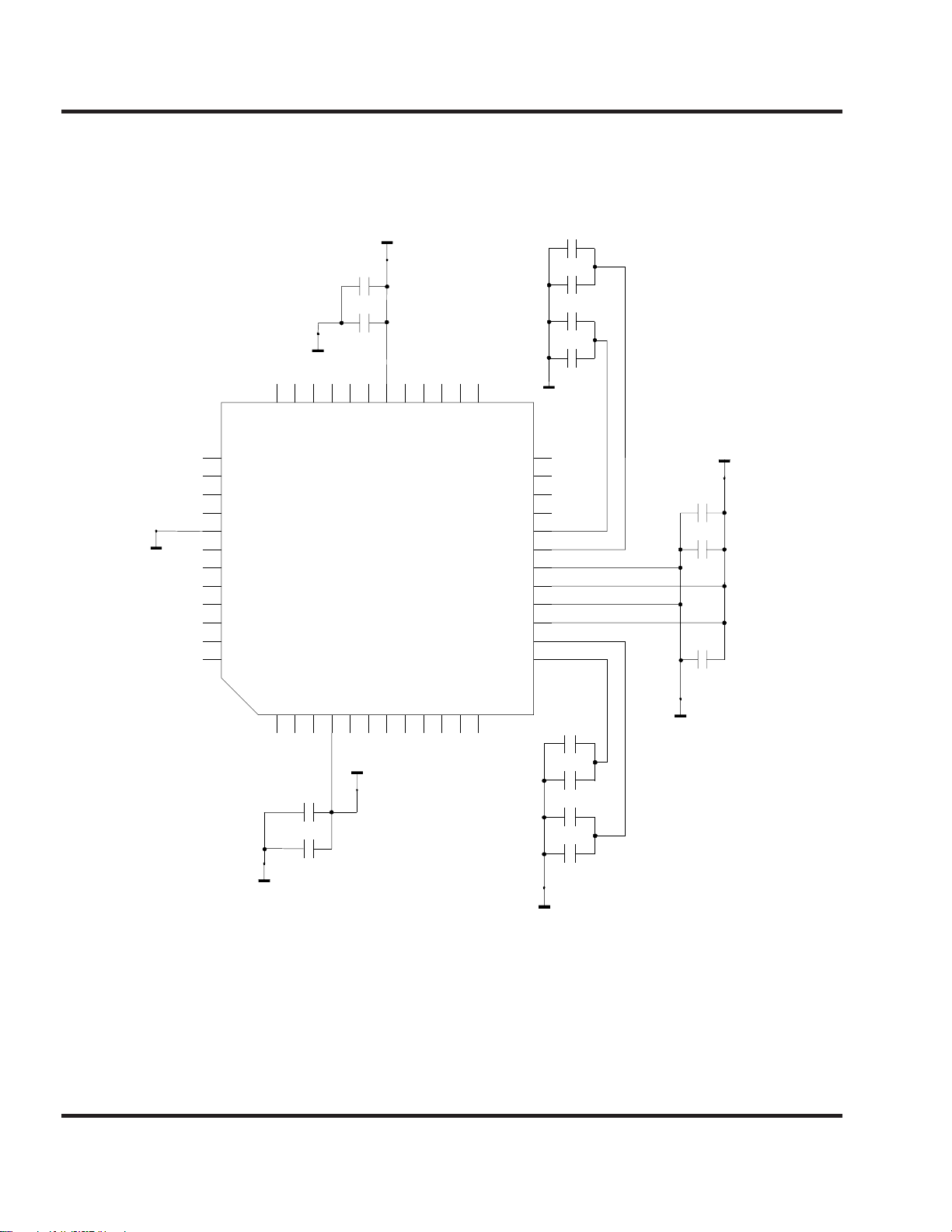
External component recommendations
DGND
37
38
39
40
41
42
43
44
45
46
47
48
CDATA3
CDATA2
CDATA1
CDATA0
DGND
OP11
OP10
OP9
OP8
OP7
OP6
OP5
DVDD
+
C13
µ
10
F
C14
µ
F
0.1
DGND
36 35 34 33 32 31 30 29 28 27 26 25
CDATA6
CDATA5
CDATA4
MCLK
CDATA7
VSMP
DVDD1
RLC
SCK/RNW
SDI/DNA
SEN/STB
WM8144-12
OEB
RINP
GINP
BINP
VMID
VRLC
AGND
AVDD
PNS
VRL
VRU
VRB
VRT
C5
22µF
C6
0.1
C7
33
C8
0.1
AGND
24
23
22
21
20
19
18
17
16
15
14
13
µ
F
++
µ
F
µ
F
AVDD
+
C1
µ
10
F
C2
µ
0.1
F
C3
µ
F
0.1
26
CC2
DV
OP0
OP1
DVDD2
OP2
OP3
OP4
123456789101112
DVDD
+
C15
µ
F
10
C16
µ
0.1
F
DGND
Wolfson Microelectronics
CC1
CC0
NRESET
ORNG
C9
10
C10
0.1
C11
10
C12
AGND
µ
µ
0.1µF
+
F
µ
F
+
F
AGND
Page 27
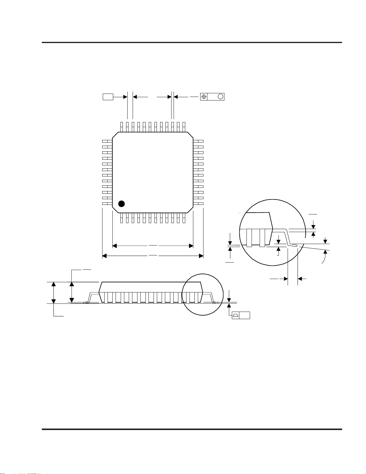
Package Dimensions
FT - 48 Pin TQFP
WM8144-12
1.45
1.35
37
48
0.50
112
7.20
6.80
9.20
8.80
0.27
0.17
2536
24
13
0.08
M
0.15
0.05
0.25
0.75
0.45
0.20
0.09
Gauge Plane
0o - 7
o
1.60MAX
Notes: A. All linear dimensions are in millimeters
B. This drawing is subject to change without notice.
C. Meets JEDEC MO-026. Refer to this specification for further details.
Wolfson Microelectronics
Seating Plane
0.08
27
 Loading...