

Page 1
Low-power Quadruple 8-Bit DAC
WM5621L
Production Data
Jan. 1997 Rev. 1.0
Description
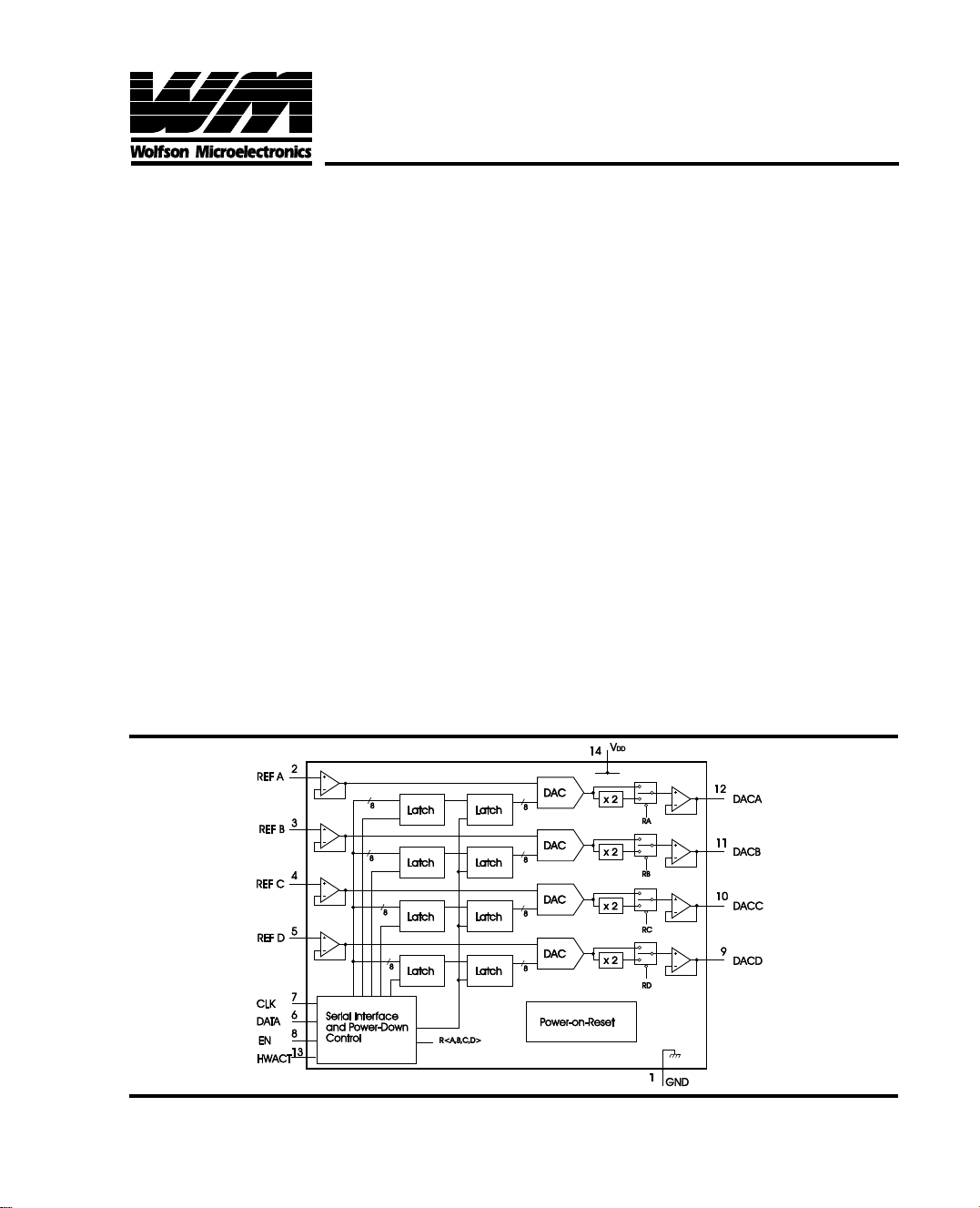
WM5621L is a quadruple 8-bit digital to analogue converter
(DAC) with buffered reference inputs (high impedance). The
DAC produces an output voltage that ranges between
either one or two times the reference voltage and GND. The
DAC is monotonic. The device operates from a single
supply in the range 2.7V to 5.5V. A power-on reset function
is incorporated to provide repeatable start-up conditions. A
global hardware shut-down terminal and the capacity to
shut-down each individual DAC with software are provided
to minimize power consumption.
WM5621L interfaces to all popular microcontrollers and
microprocessors via a three wire serial interface with CMOS
compatible, schmitt trigger, digital inputs. Alternatively a two
wire serial interface can be activated. An 11-bit command
word consists of eight bits of data, two DAC select bits and
a range bit for selection between the times one or times two
output range. The DACregisters are double buffered which
allows a complete set of new values to be written to the
device, and then under control of HWACT, all of the DAC
outputs are simultaneously updated.
Ideal in space critical applications WM5621L is available
in small outline and DIP packages and is characterized for
operation from -25
o
C to 85oC.
Block Diagram
Features
• Individual (or all) DAC's can be powered-down
• One low-power 8-bit voltage output DAC
• Three 8-bit voltage output DACs
• Fast serial interface (1 MHz max)
• Simple 2 or 3 wire interface
• Programmable for 1 or 2 times output range
• High impedance reference inputs for each DAC
• Simultaneous update facility
• Extended temperature range (-25
• Single supply operation, range 2.7 V to 5.5 V
• 0 to 4 V output (x2 output range) at 5 V V
• 0 to 2.5 V output (x2 output range) at 3 V VDD
• Low power specification:
All DACs on : 3.6 mW at 3.6 V typ
Low power DAC : 0.54 mW at 3.6V typ
All DAC's shutdown : 0.18 mW at 3.6V typ
• Guaranteed monotonic output
o
C to 85oC)
DD
: 6 mW at 5 V typ
Applications
• Mobile Communications
• Programmable d.c. voltage sources
• Digitally controlled attenuator/amplifier
• Signal synthesis
• Automatic test equipment
Production Data data sheets contain final
specifications current on publication date. Supply
of products conforms to Wolfson Microelectronics
standard terms and conditions
Wolfson Microelectronics
Lutton Court, Bernard Terrace, Edinburgh EH8 9NX, UK
Tel: +44 (0) 131 667 9386 Fax: +44 (0) 131 667 5176
email: [email protected]
www: http://www.wolfson.co.uk
© 1996 Wolfson Microelectronics
Page 2
WM5621L
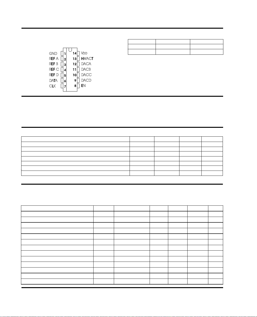
Pin Configuration
Top View
N or D Packages
GND
REFA
REFB
REFC
REFD
DATA
CLK
1
2
3
4
5
6
7
14
13
12
11
10
9
8
V
DD
HWACT
DACA
DACB
DACC
DACD
EN
Ordering Information
DEVICE TEMP. RANGE PACKAGE
WM5621LED -25oC to 85oC 14 pin plastic SO
WM5621LEN -25oC to 85oC 14 pin DIP
Absolute Maximum Ratings (note 1)
Supply Voltage (VDD - GND) . . . . . . . . . . . +7V
Digital Inputs . . . . . . . . . GND - 0.3 V, V
Reference inputs . . . . . . . GND - 0.3 V, VDD + 0.3 V
DD + 0.3 V
Operating temperature range, TA . . . . . -25oC to +85oC
Storage Temperature . . . . . . . . . -50oC to +150oC
Lead T emperature (soldering, 10 sec) . . . . . +260
Recommended Operating Conditions
MIN NOMINAL MAX UNIT
Supply Voltage 2.7 3.3 5.5 V
Reference input range GND VDD - 1.5 V
DAC output load resistance to GND 10 kΩ
High level digital input voltage 0.8 VDD V
Low level digital input voltage 0.2 VDD V
Clock frequency 1 MHz
Operating free-air temperature, TA -25 85
o
C
O
C
5
Electrical Characteristics
VDD = 3 V to 3.6V , GND = 0 V , V REF = 1.25 V , R L = 10 kΩ, CL = 100 pF, x1 gain output range, TA = full range
unless otherwise stated.
PARAMETER SYMBOL CONDITIONS MIN NOM MAX UNIT
Supply Voltage VDD see note 2 2.7 3.3 5.5 V
High level digital input voltage VIH 0.8 VDD V
Low level digital input voltage VIL 0.2 VDD V
Reference voltage, VREF [A|B|C|D] x1 gain GND VDD-1.5 V
Load resistance RL 10 kΩ
Data input setup time tSD 50 ns
Data input hold tim e tHD 5 0 ns
CLK ↓ to EN ↓
EN ↑ to CLK ↓ tLC see note 3 100 ns
CLK period high cph see note 3 400 ns
EN low time tenl 200 ns
Clock frequency fCLK 1.0 MHz
Operating free-air temperature TA -25 85
tEN see note 3 100 ns
O
C
Wolfson Microelectronics
2
Page 3
WM5621L
Electrical Characteristics (continued)
VDD = 3 V to 3.6V, GND = 0 V, VREF = 1.25 V , RL = 10 kΩ, CL = 100 pF , x1 gain output range, TA = full range
unless otherwise stated.
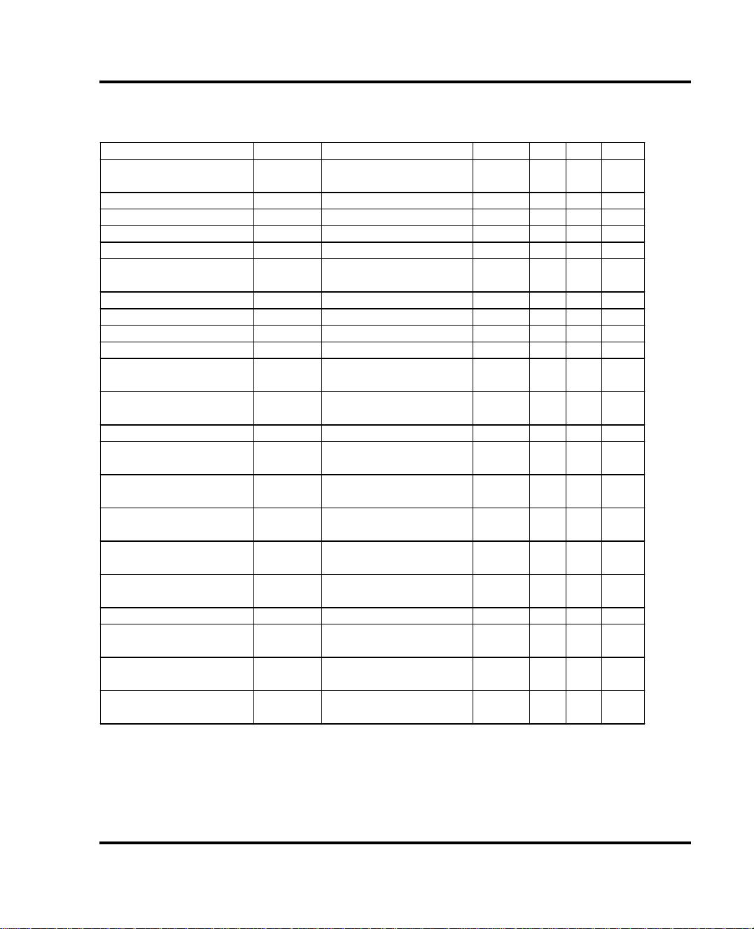
PARAMETER SYMBOL CONDITIONS MIN TYP MAX UNIT
Max. full-scale output voltage Vomax Vref=1.5V, open cct. output VDD-100 2 mV
,x 2 gain
High level input current IIH VI = VDD ± 10µA
Low level input current IIL VI = 0V ± 10
Output sink current DACA Io (sink) at DAC code 0 5 µA
Output sink current DACB Io (sink) at DAC code 0 20 µA
Output Source Current Io (source) Each DAC output, at DAC 1 mA
code 255
Input capacitance CI 15 pF
Re ference in put capaci t ance A, B, C , D inputs 15 pF
Supply current IDD VDD = 3.6V 1 1.5 mA
VDD = 5.0V 1 1.5 mA
Supply current One low IDAC VDD = 3.6V (Note 4) 150 250 µA
power DAC Active
Supply Current ALL DACs Iddsd VDD = 3.6V (see note 4) 50 100
Shutdown
Reference input current IREF A, B, C, D inputs ± 10 µA
Integral Nonlinearity INL VREF = 1.25V, Range x2. ± 1.0 LSB
(note 5,13)
Differential Nonlinearity DNL VREF = 1.25V, Range x2. ± 0.1 ± 0.9 LSB
(note 6,13)
Zero scale error ZCE VREF = 1.25V,Range x2 . 0 30 mV
(note 7)
Zero scale error tempera t ure VREF = 1.25V,Input code = 00 10
coefficient Hex (note 8)
Zero scale error supply 2 mV/V
rejection
Full scale error FSE Range x 2. (note 9) ± 60 mV
Full scale error temperature VREF = 1.25V,Range x2. ± 25
coeffic i ent (note 10 )
Full sca le error su pply 2 mV/V
reje ct ion
Feedback resistor network 168
resistance
Notes:
1. Absolute Maximum Ratings are stress ratings only.
Permanent damage to the device may be caused by
continuously operating at or beyond these limits. Device functional operating range limits are given under
Recommended Operating Conditions. Guaranteed
performance specifications are given under Electrical
Characteristics at the test conditions specified.
2. The device operates over the supply voltage range of
2.7V to 5.5V. Over this voltage range the device responds correctly to data input by changing the voltage
output but conversion accuracy is not specified over
this extended range.
µA
µA
µV/
µV/
kΩ
O
C
O
C
Wolfson Microelectronics
3
Page 4

5
WM5621L
Electrical Characteristics
VDD = 3 V to 3.6V, GND = 0 V, VREF = 1.25 V, RL = 10 kΩ, CL = 100 pF, x1 gain output range, TA = full range
unless otherwise stated.
PARAMETER SYMBOL CONDITIONS MIN TYP MAX UNIT
Output slew rate rising DACA 0.8
Output slew rate falling DACA 0.5
Output slew rate DACB,C,D 1
Output settling time rising To 1/2 LSB, VDD=3V 20 µS
DACA
Output settling time falling To 1/2 LSB, VDD=3V 75 µS
DACA
Output settling time rising To 1/2 LSB, VDD=3V 10 µS
DACB,C,D
Output settling time falling To 1/2 LSB, VDD=3V 75 µS
DACB,C,D
Output se t tling time HWACT To 1/2 LSB , V DD=3V 40 120* µS
or ACT ↑ to output volts DACA
(note 14)
Output se t tling time HWACT To 1/2 LSB , V DD=3V 25 75*
or ACT ↑ to output volts
DACB,C,D (note 14)
Large signal Bandwidth Measured at -3dB point 100 KHz
Digital crossta lk CLK=1 MHz sq. w ave -50 dB
meas ured at D ACA-DACD
Refer ence feedthrough A,B,C,D in puts (not e 15) -60 dB
Cha nnel-to- channel iso l ation A, B,C,D in put s (n ot e 16) -60 dB
Cha nnel-to- channel iso l ation A,B,C,D in puts -40 dB
when in shutdown
Reference bandwidth DACA note 17 20 kHz
Reference bandwidth note 17 100 kHz
DACB,C,D
V/µS
V/µS
V/µS
µS
Notes:
3. This is tested by design but is not production tested.
4. This is measured with no load (open circuit output),
Vref = 1.25V , range = x2.
5. Integral Nonlinearity (INL) is the maximum deviation of
the output from the line between zero and full scale (excluding the effects of zero code and full-scale errors).
6. Differential Nonlinearity (DNL) is the difference between the measured and ideal 1 LSB amplitude
change of any two adjacent codes. A guarantee of
monotonicity means the output voltage changes in the
same direction (or remains constant) as a change in
the digital input code.
Wolfson Microelectronics
4
7. Zero-scale error is the deviation from zero voltage
output when the digital input code is zero.
8. Zero scale error temperature coefficient is given by:
ZCETC = (ZCE(T
(Tmax - Tmin)
9. Full-Scale error is the deviation from the ideal full-scale
output (Vref - 1LSB) with an output load of 10kΩ.
10. Full-Scale T emperature Coefficient is given by:
FSETC = (FSE(T
(Tmax - Tmin)
11. Zero-code Error Rejection Ratio (ZCE-RR) is
measured by varying the V
5.25 V d.c., and measuring the proportion of this
signal imposed on the zero-code output voltage.
max) - ZCE(Tmin))/VREF
max) - FSE(Tmin))/VREF x 10
DD voltage, from 4.75 to
x 106/
6
/
Page 5
Electrical Characteristics (continued)
WM5621L
12. Full Scale Error Rejection Ratio (FSE-RR) is
measured by varying the VDD voltage, from 4.75 to
5.25 V d.c., and measuring the proportion of this
signal imposed on the full-scale output voltage.
13. Linearity is only specified for DAC codes 1 through
255.
14. The ACT bit is latched on falling edge of EN.
15. Reference feedthrough is measured at any DAC output with an input code = 00 hex with a Vref input = 1Vdc
+ 1 Vpp at 10kHz.
16. Channel-to-channel isolation is measured by setting
the input code of one DAC to FF hex and the code of
all other DACs to 00 hex with Vref input = 1Vdc + 1
Vpp at 10kHz.
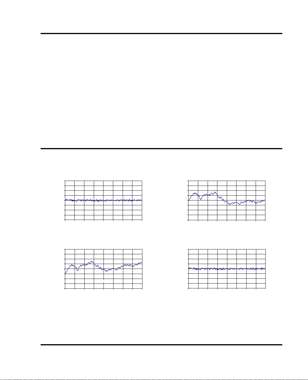
Typical Performance Characteristics
Typical DNL, INL and TUE at VDD = 5 V
Vdd = 5.0V, Vref = 2.5V, Range = x1 @
25'C
Error (LSBs)
Differential Nonlinearity
VDD = 5.0, VREF = 2.5V, Range = x1 at 25oC
0.2
0.15
0.1
0.05
0
Error (lsbs)
-0.05
-0.1
-0.15
-0.2
0 32 64 96 128 160 192 224 256
Code
Input Code
17. Reference bandwidth is the -3dB bandwidth with an
ideal input at Vref = 1.25 Vdc + 2 Vpp and with a digital input code of full-scale (range set to x1 and Vdd =
5V)
Integral Nonlinearity
Vdd = 5 .0V, Vre f = 2. 5V, Ra nge = x1 @ 25 'C
VDD = 5.0, VREF = 2.5V, Range = x1 at 25oC
0.2
0.15
0.1
0.05
0
Erro r (lsbs)
-0.05
Error (LSBs)Error (LSBs)
-0.1
-0.15
-0.2
0 32 64 96 128 160 192 224 256
Integr al Non Line arity
Code
Input Code
Total Unadjusted Error
Vdd = 5.0 V, Vref = 2.5 V, Rang e = x 1 @ 25' C Differe nti al Non Li nea ri ty
VDD = 5.0, VREF = 2.5V, Range = x1 at 25oC
0.2
0.15
0.1
0.05
0
Error (lsbs)
-0.05
Error (LSBs)
-0.1
-0.15
-0.2
0 32 64 96 128 160 192 224 256
Total Unadjusted Error
Code
Input Code
Vd d = 5.0V, Vref = 2.0V, Range = x2 @ 25'C
0.15
0.05
Error (lsbs)
-0.05
-0.1
-0.15
-0.2
Differential Nonlinearity
VDD = 5.0, VREF = 2.0V, Range = x2 at 25oC
0.2
0.1
0
0 32 6 4 96 1 28 160 1 92 224 2 56
Wolfson Microelectronics
Code
Input Code
5
Page 6
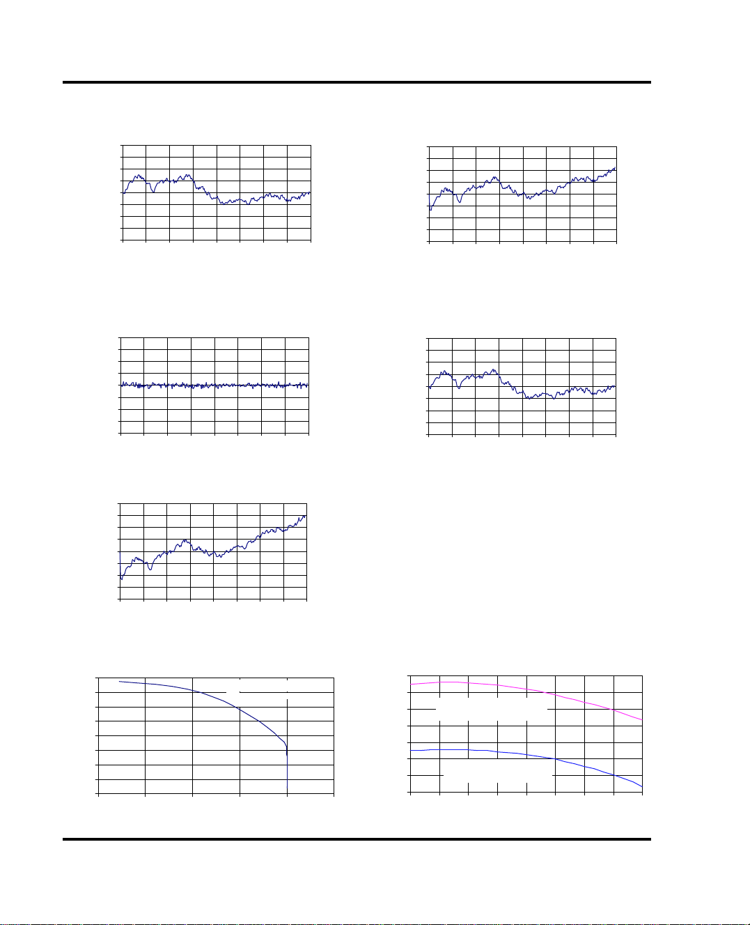
WM5621L
Typical Performance Characteristics (continued)
5
Integral Nonlinearity
Vdd = 5 .0V, Vre f = 2 .0V, Ran ge = x2 @ 25' C
VDD = 5.0, VREF = 2.0V, Range = x2 at 25oC
0.2
0.1 5
0.1
0.0 5
0
Error (lsbs)
-0.05
Error (LSBs)
-0.1
-0.15
-0.2
0 32 64 96 128 160 192 224 256
Integr al Non Lin e arit y
Code
Input Code
Typical DNL, INL and TUE at VDD = 3 V
Differential Nonlinearity
Vdd = 3.0 V, Vref = 1.2 5V , Ran ge = x2 @ 25'C
VDD = 3.0, VREF = 1.25V, Range = x2 at 25oC
0.2
0.15
0.1
0.05
0
Error (lsbs)
-0.05
Error (LSBs)
-0.1
-0.15
-0.2
0 32 64 96 128 160 192 224 256
Total Unadjusted Error
Vdd = 3. 0V, Vre f = 1. 25 V, Ra nge = x 2 @ 25 'C
VDD = 3.0, VREF = 1.25V, Range = x2 at 25oC
0.2
0.15
0.1
0.05
0
Error (lsbs)
-0.05
Error (LSBs)
-0.1
-0.15
-0.2
0 32 64 9 6 128 160 192 224 256
Differential Non Linearity
Code
Input Code
Total Unadjusted Error
Code
Input Code
Total Unadjusted Error
Vd d = 5.0V, Vref = 2.0V, Range = x2 @ 25'C
VDD = 5.0, VREF = 2.0V, Range = x2 at 25oC
0.2
0.15
0.1
0.05
0
Error (lsbs)
-0.05
-0.1
Error (LSBs)
-0.15
-0.2
0 32 64 96 128 160 192 2 24 256
Vd d = 3.0V, Vr ef = 1.25V, Range = x2 @ 25'C
VDD = 3.0, VREF = 1.25V, Range = x2 at 25oC
0.2
0.15
0.1
0.05
0
Error (lsbs)
-0.05
-0.1
Error (LSBs)
-0.15
-0.2
0 32 64 96 128 160 192 2 24 256
Total Unadjusted Error
Code
Input Code
Integral Nonlinearity
Integr al Non Line arity
Code
Input Code
Output Source Current vs Output Voltage
VDD = 5.0, VREF = 2V, Range = 2x, Input Code = 255, Temperature = 25oC
8
7
Vdd = 5V, Vref = 2.0V, Ran ge = 2x
Inpu t Code = 255, Temp erature = 25'C
6
5
4
Iout (mA)
3
IOUT (mA)
2
1
0
012345
Vou t (V)
VOUT (V)
Wolfson Microelectronics
6
Supply Current v Temperature
Supply Current vs Temperature
1.15
1.1
1.05
Vdd = 5V, Vref = 2.0V
VDD = 5.0, VREF = 2V,
Range = 2x, Input Code = 255
Range = 2x, Input Code = 255
1
IDD (mA)
0.95
IDD (mA)
0.9
0.85
Vdd = 3V, Vref = 1.25V
VDD =3.0, VREF = 1.25V,
Range = 2x, Input Code =
Range = 2x, Input Code = 255
255
0.8
-30-150 153045607590
Temperature ('C)
Temperature (oC)
Page 7
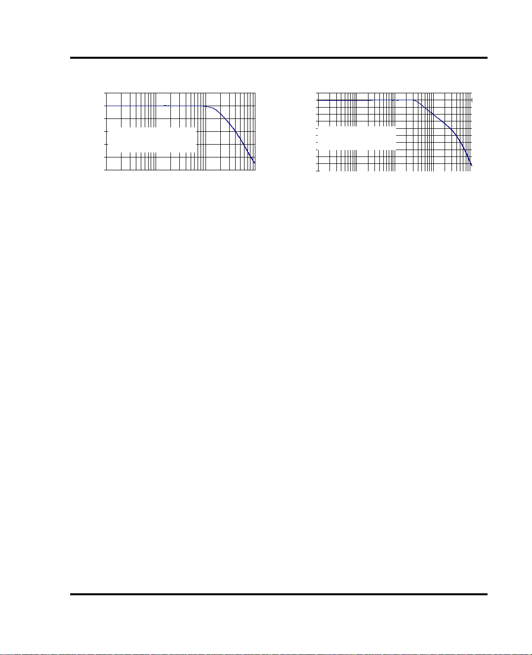
Typical Performance Characteristics (continued)
Large Signal Frequency Response
5
0
-5
Vdd = 5V, Vref = 1.25V + 2V pp
-10
VDD = 5.0, VREF = 1.25V + 2Vpp,
Range = 1x, Input Code = 255
Range = 1x, Input Code = 255
Relative Gain (dB)
Tempera ture = 25'C
-15
Temperature = 25
Relative Gain (dB)
-20
-25
1000 10000 100000 1000000
Large Signal Freque ncy Response
5
0
-5
-10
-15
-20
-25
o
C
Frequency (KHz)
Frequency (KHz) Frequency (KHz)
Relative Gain (dB)
-30
-35
Relative Gain (dB)
-40
-45
-50
WM5621L
Small Signal Frequency Response
VDD = 5V, VREF = 2V + 1Vpp,
Vdd = 5V, Vref = 2V + 1 V pp
Range = 1x, Input Code = 255
Range = 1x, Input Code = 255
Temperatur e = 25'C
Temperature = 25
1 10 100 1000 10000
Sm al l S ig na l F re q uenc y Re sp ons e
o
C
Frequency ( KHz)
Wolfson Microelectronics
7
Page 8
5
WM5621L
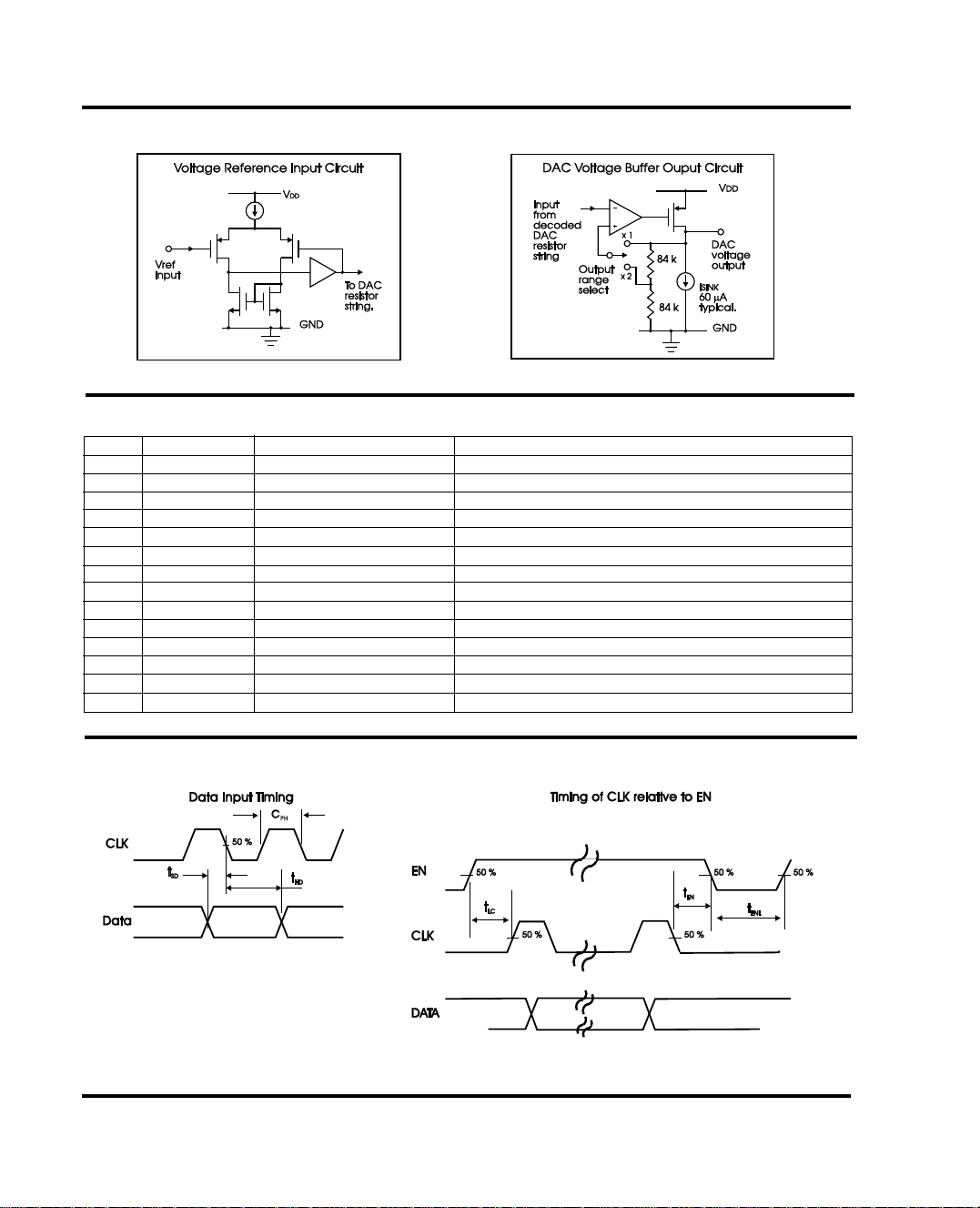
Input and Output Circuits
Pin Descriptions
Pin Name Type Function
1 GND Supply Ground return and reference terminal
2 REFA Analogue input Reference voltage input to DACA
3 REFB Analogue input Reference voltage input to DACB
4 REFC Analogue input Reference voltage input to DACC
5 REFD Analogue input Reference voltage input to DACD
6 DAT A Digital input Serial interface data
7 CLK Digital input Serial interface clock, negative edge sensitive
8 EN Digital input Input Enable
9 DACD Analogue output DAC D output
10 DACC Analogue output DAC C output
1 1 DACB Analogue output DAC B output
12 DACA Analogue output DAC A output
13 HWACT Digital input Hardware activate
14 VDD Supply Positive supply voltage
Timing Waveforms
8
Figure 1: Detailed timing of serial interface
Wolfson Microelectronics
Page 9
WM5621L
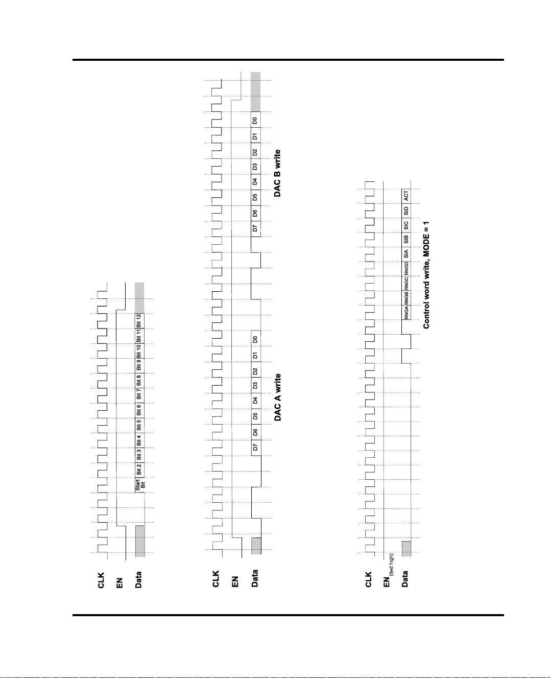
Figure 2: Serial write in double buffered mode. Registers are latched on falling edge of EN. Preceding ZEROs on DATA are ignored.
Wolfson Microelectronics
falling edge of EN.
falling edge of CLK after a Start Bit has been detected.
Figure 3: Multiple DAC updates at the same time are possible by holding EN high over multiple serial words. All DACs are updated on the
Figure 4: In single buffered mode, synchronisation can be regained by clocking in at least 12 ZEROs. Registers are updated on the twelfth
9
Page 10

WM5621L
Functional Description
5
DAC operation
Each of WM5621L's four digital to analogue converters
(DACs) are implemented using a single resistor string with
256 taps corresponding to each of the input 8-bit codes.
One end of a resistor string is connected to the GND pin
and the other end is driven from the output of a reference
input buffer. The use of a resistor string guarantees
monotonicity of the DAC's output voltage. Linearity depends
upon the matching of the resistor string's individual elements
and the performance of the output buffer. The reference input
buffers present a high impedance to reference sources.
Each DAC has a voltage output amplifier which is
programmable for gains of x1 or x2 through the serial
interface. The DAC output amplifiers feature rail to rail
output stages, allowing outputs over the full supply voltage
range to be achieved with a x2 gain setting and a VDD/2
reference voltage input. Used in this way a slight
degradation in linearity will occur as the output voltage
approaches VDD.
Control of the WM5621L is effected through a serial
interface using three dedicated pins, CLK, DAT A and EN.
A fourth pin (HWACT) is used to control the power-down
controls to each of the 4 DACs.
Serial Interface
The serial interface uses the CLK pin to clock in data words
presented serially on the DATA pin. The data words are
12 bits long and are written to either a control register or
to one of the four DAC registers. When the EN pin is held
low the serial interface is held in reset.
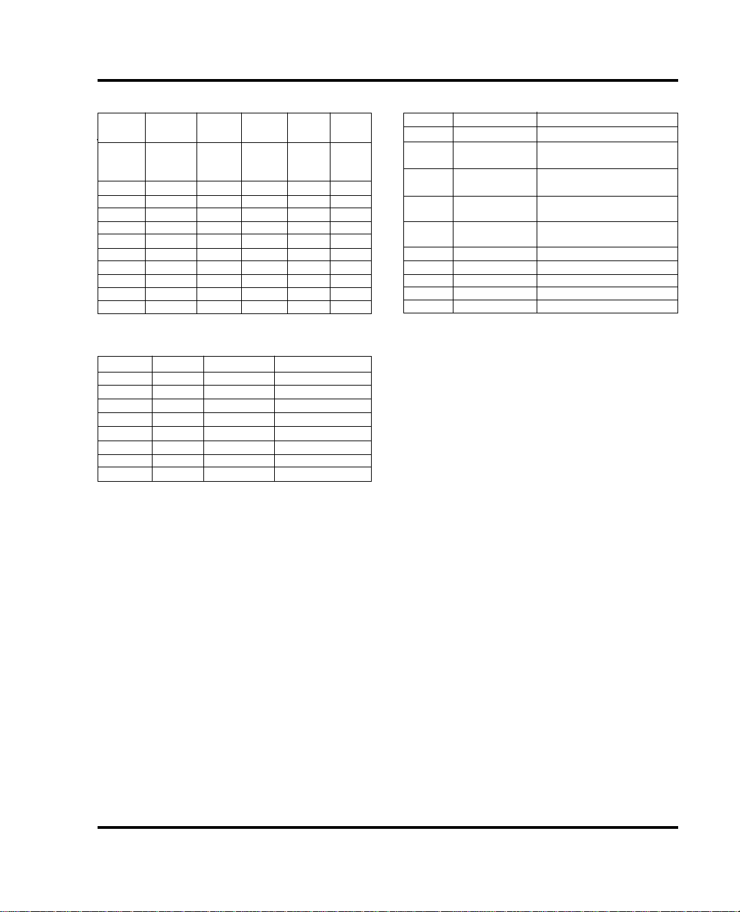
Figure 1 shows the format of the 12-bit data word transfer
into the WM5621L. DAT A is clocked on the falling edge of
CLK. Every data word must start with a high start bit
(preceeding zeros are ignored). The second bit is the
register select bit which selects a write into either the
control register or one of the DAC registers. Table 1 shows
all valid write sequences.
Double Buffered Mode
In normal operation the EN signal is used to control the
latching of data. All DAC registers and all bits of the
control word (other than MODE) are double buffered, with
the second buffer only being enabled when the EN pin is
taken low. In this way it is possible to update any number
of DAC inputs at once by writing a 12-bit word to update
each DAC register, with EN held high for all writes. When
EN is pulled low at the end of the last write, all DAC inputs
are latched at the same time. Figure 3 shows DACs A
and B being written to in this way.
This mode also allows multiple devices to be share DATA
and CLK lines by having only separate EN lines.
Single Buffered Mode
If the device is to be operated in single buffered mode, the
EN pin should be tied high, and the interface is always
active. The first write to the device after power-on should
be a write to the control register to set the MODE bit high.
The double buffered action is not possible as all words
are latched across on the twelfth falling edge of CLK.
Loss of synchronisation may occur if glitches are present
on the CLK and DATA inputs, a condition which may
occur at power-on. If this has happened it is possible to
regain synchronisation by clocking in at least 12 zeros
(see Figure 4).
It is not possible to reset the MODE bit from 1 to 0.
Operation of the device after any attempt to do this is
undefined.
DAC Registers
Each DAC register holds an 8-bit unsigned byte to
represent the DAC code. Table 1 indicates how these
bytes are clocked into the DAC registers, with D7 being
the most significant bit of the byte. These registers are
reset to 0 at power-on.
The serial interface can operate in one of two ways,
controlled by the setting of the MODE bit in the control
register. The MODE bit defaults to 0 on power up which sets
the device to work in a double buffered mode. When MODE
is set to 1, the device operates in a single buffered mode,
which can be controlled through only two pins (DAT A and
CLK, EN held high).
Wolfson Microelectronics
10
Page 11
Functional Description (continued)
WM5621L
Bit Control DACA DACB DACC DACD
Word Write Write Write Write
Start Bit 1 1 1 1 1
Register 0 1 1 1 1
Select
3 MODE 0 0 1 1
4 RNGA 0 1 0 1
5 RNGB D7 D7 D7 D7
6 RNGC D6 D6 D6 D6
7 RNGD D5 D5 D5 D5
8 SIA D4 D4 D4 D4
9 SIB D3 D3 D3 D3
10 SIC D2 D2 D2 D2
11 SID D1 D1 D1 D1
12 ACT D0 D0 D0 D0
Table 1
SIA ACT HWACT DAC status
0 0 0 shutdown
0 0 1 shutdown
0 1 0 shutdown
0 1 1 active
1 0 0 active
1 0 1 active
1 1 0 active
1 1 1 active
Table 3
Control Register
The control register contains 10 active bits. The MODE bit
controls the operation of the serial interface as described
above. The function of the control register bits, and their
state on power-up, are shown in table 2.
The shutdown state of each DAC is controlled through the
shutdown inhibit bit for that channel (SIx), the ACT bit of the
control register, and the HWACT pin. Table 3 shows the
logical action of these three controlling bits for DAC A. It is
possible, for example, to have any combination of DACs
switched from shutdown to active by the HWACT pin, while
the remaining DACs are held always active (achieve this by
setting ACT=1, SIx=0 for the switching DACs, and SIx=1 for
the always active DACs).
Bit Power-up state Function
MODE 0 Control serial interface
RNG A 1 DACA range select
(0 = x1, 1 = x2)
RNG B 1 DACB range select
(0 = x1, 1 = x2)
RNG C 1 DACC range select
(0 = x1, 1 = x2)
RNG D 1 DACD range select
(0 = x1, 1 = x2)
SIA 0 DACA shutdown inhibit
SIB 0 DACB shutdown inhibit
SIC 0 DACC shutdown inhibit
SID 0 DACD shutdown inhibit
ACT 0 Software shutdown control
Table 2
Linearity, offset, and gain error using
single end supplies
When an amplifier is operated from a single supply, the
voltage offset can still be either positive or negative. With
a positive offset, the output voltage changes on the first
code change. With a negative offset the output voltage
may not change with the first code depending on the
magnitude of the offset voltage.
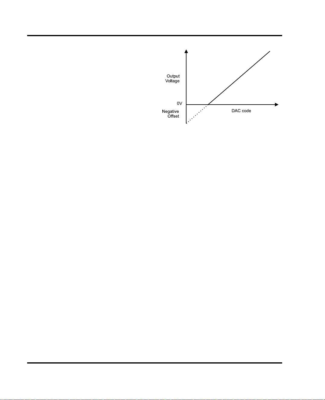
The output amplifier, with a negative voltage offset,
attempts to drive the output to a negative voltage.
However, because the most negative supply rail is GND,
the output cannot drive to a negative voltage.
So when the output offset voltage is negative, the output
voltage remains at ZERO volts until the input code value
produces a sufficient output voltage to overcome the
inherent negative offset voltage, resulting in the transfer
function shown in Figure 5.
This negative offset error, not the linearity error, produces
this breakpoint. The transfer function would have followed
the dotted line if the output buffer could drive to a negative
voltage.
Wolfson Microelectronics
11
Page 12
WM5621L
Functional Description (continued)
For a DAC, linearity is measured between ZERO input code
( all inputs 0 ) and full scale code ( all inputs 1 ) after offset
and full scale are adjusted out or accounted for in some
way. However, single supply operation does not allow for
adjustment when the offset is negative due to the breakpoint in the transfer function. So the linearity in the unipolar
mode is measured between full scale code and the lowest
code which produces a positive output voltage. The code
is calculated from the maximum specification for the
negative offset.
Figure 5: Effect of negative offset (single supply)
5
Wolfson Microelectronics
12
Page 13
Package Descriptions
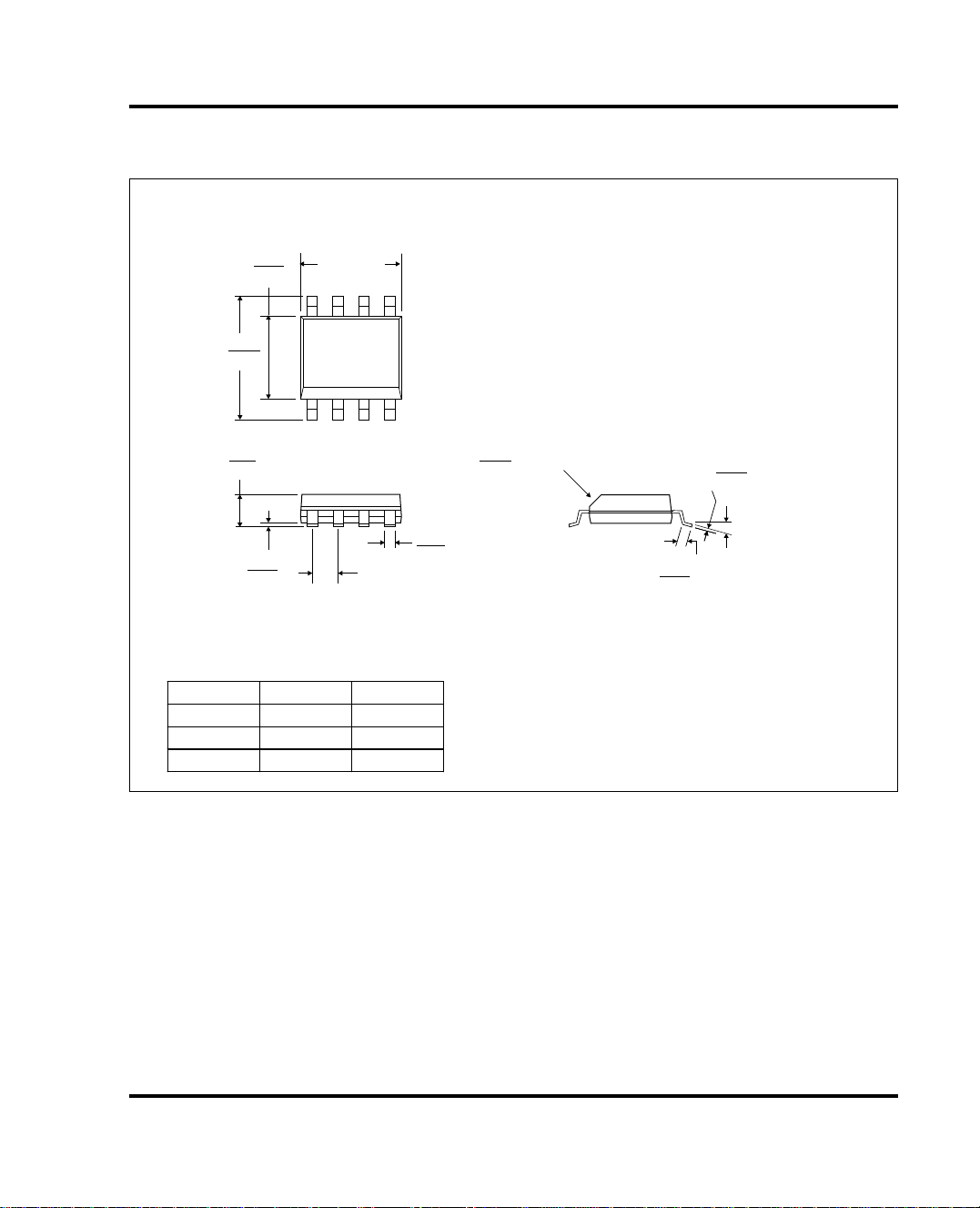
Plastic Small-Outline Package
D - 8 pins shown
WM5621L
4.00
3.80
6.20
5.80
1.75
1.35
0.25
0.10
A
58
14
Pin spacing
1.27 B.S.C.
Dimension 'A' Variations
NMinMax
8 4.80 5.00
14 8.55 8. 75
16 9.80 10.00
0.51
0.33
0.50
0.25
O
x 45 NOM
1.27
0.40
0.25
0.19
OO
0 to 8
Notes:
A. Dimensions in millimeters.
B. Complies with Jedec standard MS-012.
C. This drawing is subject to change without notice.
D. Body dimensions do not include mold flash or protrusion.
E. Dimension A, mould flash or protrusion shall not exceed 0.15mm. Body width, interlead flash or protrusions shall
not exceed 0.25mm.
Rev. 1 November 96
Wolfson Microelectronics
13
Page 14
WM5621L
Package Descriptions
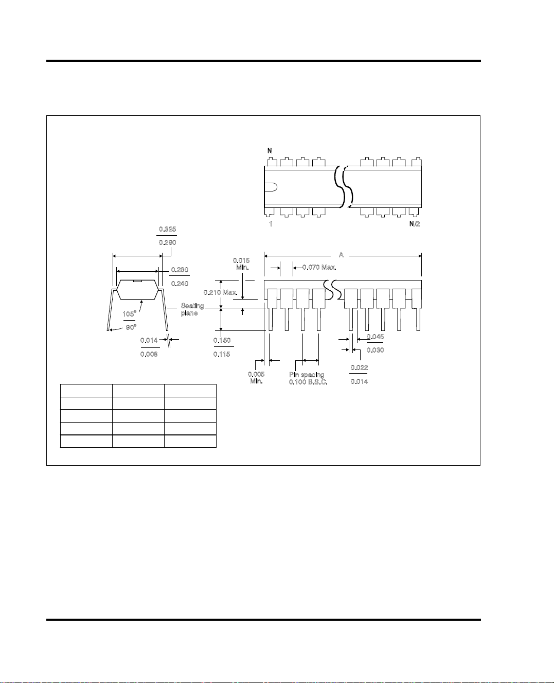
Dual-In-Line Package
N or P
N
5
0.005
Min.
1
0.070 Max.
Pin spacing
0.100 B.S.C.
A
0.045
0.030
0.022
0.014
O
105
O
90
0.014
0.008
Dimension 'A' Variations
0.325
0.290
0.280
0.240
Seating
plane
0.210 Max.
0.150
0.115
0.015
Min.
NMinMax
8 0.355 0.400
14 0.735 0.775
16 0.735 0.775
20 0.940 0.975
Notes:
A. Dimensions are in inches
B. Falls within JEDEC MS-001( 20 pin package is shorter than MS-001)
C. N is the maximum number of terminals
D. All end pins are partial width pins as shown, except the 14 pin package which is full width.
N/2
14
Rev. 1 November 96
Wolfson Microelectronics
 Loading...