

Page 1
10-Bit Digital-to-Analogue Converter
WM5615
Production Data
January 1997 Rev 2
Description
The WM5615 is a 10-bit voltage output digital-toanalogue converter (DAC) with a buffered reference input
(high impedance). The DAC produces a maximum output
voltage that is twice the reference voltage and the DAC is
monotonic. The device is simple to use, running from a
single supply of 5V. A power-on reset function is
incorporated to ensure repeatable start-up conditions.
Digital control of the WM5615 is over a 3-wire serial bus
that is CMOS compatible and easily interfaced to industry
standard microprocessor and microcontroller devices. The
device receives a 16-bit data word to produce the
analogue output. The digital inputs feature Schmitt
triggers for high noise immunity. Digital communication
protocols include the SPITM, QSPITM and MicrowireTM standards.
The 8-terminal small-outline D package allows digital
control of analogue functions in space-critical applications.
The WM5615C is characterised for operation from 0oC to
o
C. The WM5615I is for operation from -40oC to 85oC.
70
SPI and QSPI are trademarks of Motorola, Inc. Microwire is a trademark of
National Semiconductor Corp.
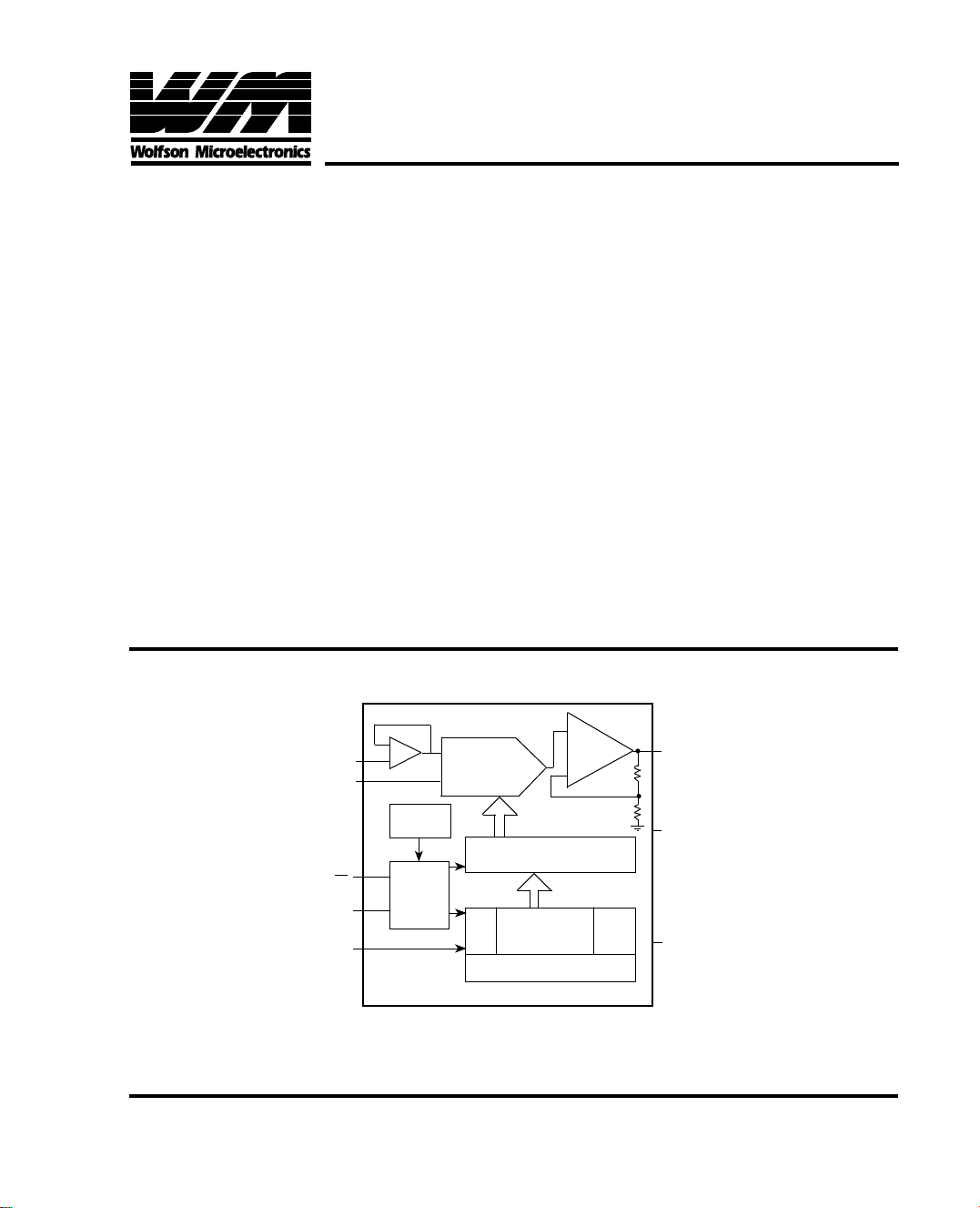
Block Diagram
REFIN
AGND
CS
SCLK
DIN
+
POWER-ON
RESET
CONTROL
LOGIC
RESISTOR
STRING
DAC
2
Xs
Features
• 10-bit CMOS voltage output DAC in an
8-terminal package
• 5V single supply operation
• 3-wire serial interface
• High-impedance reference input
• Maximum voltage output twice reference
input voltage
• Internal power-on reset
• Low power consumption ... 1.75mW max
• 877kHz update rate
• Setting time to 0.5 LSB ... 12.5
µµ
µs typical
µµ
• Monotonic over temperature
• Pin compatible with the Maxim MAX515
Applications
• Battery-powered test Instruments
• Digital offset and gain adjustment
• Battery-operated/remote industrial controls
• Machine and motion control devices
• Cellular telephones
+
VOUT
R
-
R
VDD
10-BIT DAC REGISTER
(LSB)
16-BIT SHIFT REGISTER
(MSB)
4
DUMMY
BITS
DOUT
5
Production Data data sheets contain final
specifications current on publication date.
Supply of products conforms to Wolfson Microelectronics standard terms and conditions.
Wolfson Microelectronics
Lutton Court, Bernard Terrace, Edinburgh EH8 9NX. UK
Tel: +44 (0) 131 667 9386 Fax: +44 (0) 131 667 5176
email: [email protected]
www: http://www.wolfson.co.uk
© 1996 Wolfson Microelectronics
Page 2
WM5615
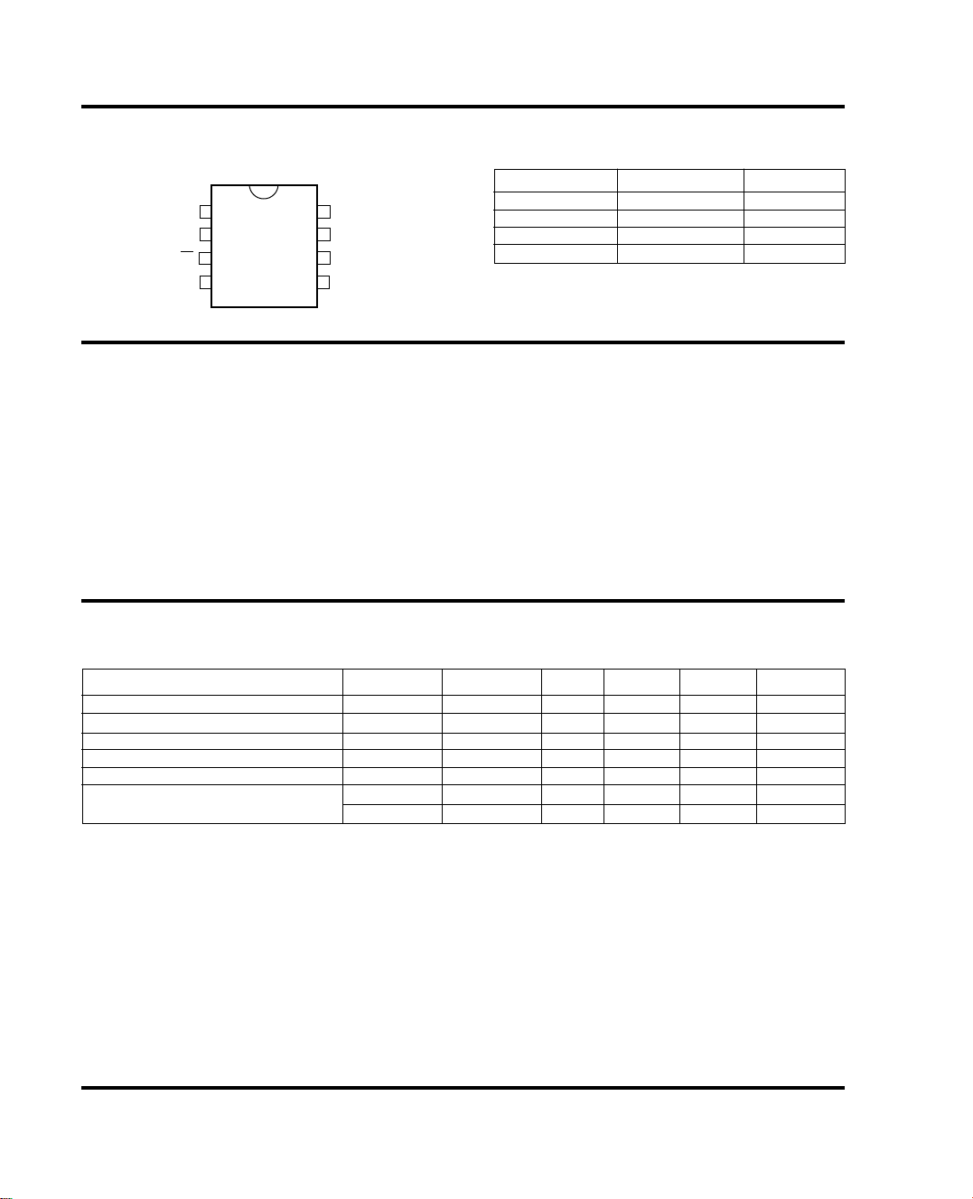
Ordering InformationPin Configuration
D or P package
Top View
DIN
SCLK
DOUT
1
2
CS
3
4
8
7
6
5
V
DD
VOUT
REFIN
AGND
Absolute Maximum Ratings
Supply voltage (VDD to AGND) . . . . . . . . . . . . 7V
Digital input voltage range to AGND . .-0.3V to V
Ref. input voltage range to AGND . . .-0.3V to V
Output voltage at OUT from external source . .VDD + 0.3V
Continuous current, any terminal . . . . . . . . ±20mA
Note: Stresses beyond those listed under 'Absolute Maximum Ratings' may cause damage to the device. These are
stress ratings only, and functional operation of the device at these or any other conditions beyond those indicated
under 'Recommended Operating Conditions' is not implied. Exposure to absolute maximum rated conditions for
extended periods may affect device reliability.
DD +0.3V
DD + 0.3V
DEVICE TEMP RANGE PACKAGE
WM5615CD 0oC to +70oC 8 pin SO
WM5615CP 0
WM5615ID -40
WM5615IP -40
Operating free-air temperature range TA:
WM5615C . . . . . . . . . . . . . . . . . . 0oC to +70oC
WM5615I . . . . . . . . . . . . . . . . . -40
Storage temperature range T
Lead temperature 1.6mm (1/16 inch)
from case for 10 seconds . . . . . . . . . . . . . .260
o
C to +70oC 8 pin DIP
o
C to +85oC 8 pin SO
o
C to +85oC 8 pin DIP
o
C to +85oC
stg . . . . . -65
o
C to +150oC
o
C
Recommended Operating Conditions
PARAMETER SYMBOL MIN TYP MAX UNIT
Supply voltage V
DD 4.5 5 5.5 V
High-level digital input voltage VIH 2.4 V
Low-level digital input voltage VIL 0.8 V
Reference voltage to REFIN terminal Vref 0 2.048 VDD-2 V
Load resistance RL 2kΩ
Operating free air temperature WM5615C TA 070
WM5615I TA -40 85
o
C
o
C
Wolfson Microelectronics
2
Page 3
WM5615
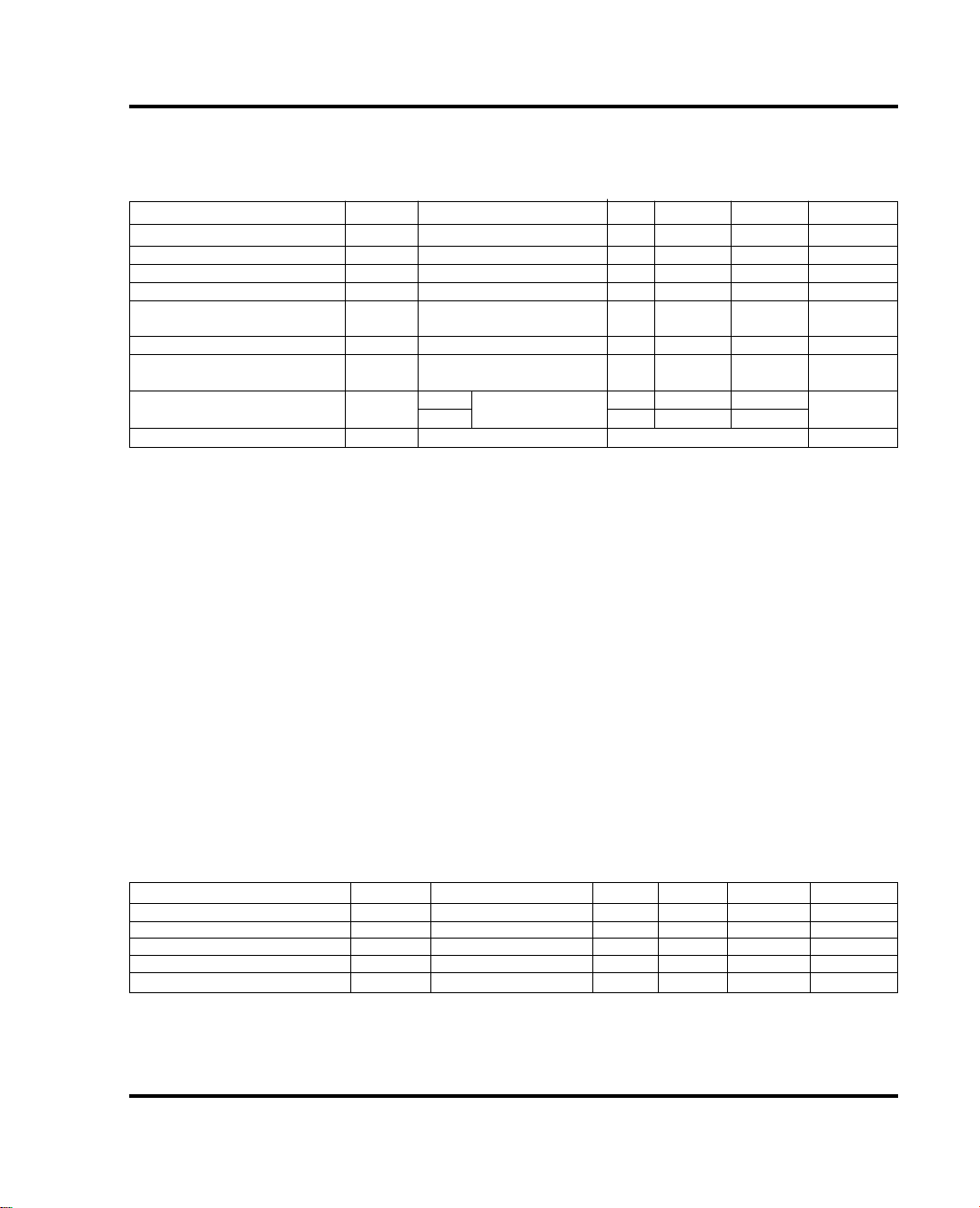
Electrical Characteristics (over recommended operating free-air temperature range)
VDD = 5.0V ±5%, Vref = 2.048V unless otherwise stated.
Static DAC Specifications
PARAMETER SYMBOL CONDITIONS MIN TYP MAX UNIT
Resolution 10 bits
Integral nonlinearity INL (see note 1) ±1 LSB
Differential nonlinearity DNL (see note 2) +0.1 ±0.5 LSB
Zero scale error (offset error) EZS (see note 3) ±3 LSB
Zero scale error (offset error) (see note 4) 3 ppm/oC
temperature coefficient
Gain error EG (see note 5) ±3 LSB
Gain error temperature (see note 6) 1 ppm/oC
coefficient
Power-supply rejection ratio PSRR Offset (see notes 7 and 8) 0.1 LSB/V
Gain 0.1
Analogue full scale output RL = 100kΩ 2Vref(1023/1024) V
Notes:
1. The relative accuracy or integral nonlinearity (INL),
sometimes referred to as linearity error, is the
maximum deviation ot the output from the line
between zero and full scale, excluding the effect of
zero code and full scale errors (see text).
2. The differential nonlinearity (DNL), sometimes
referred to as differential error, is the difference
between the measured and ideal LSB amplitude
change of any two adjacent codes. Monotonic means
the output voltage changes in the same direction (or
remains constant) as a change in the digital input
code.
3. Zero-scale error is the deviation from zero voltage
output when the digital input is zero (see text)
4. Zero-scale error temperature coefficient is given by
EZS TC = [EZS (Tmax) - EZS (Tmin)] /Vref x 106/ (Tmax-
Tmin)
5. Gain error is the deviation from the ideal output (Vref
- 1LSB) with an output load of 10kΩ, excluding the
effects of zero error.
6. Gain temperature coefficient is given by EG TC =
G (Tmax) - EG (Tmin)] /Vref x 10
[E
7. Zero-scale offset error rejection ratio (E
measured by varying the V
and measuring the proportion of this signal imposed
on the zero-code output voltage.
8. Gain error rejection ratio (E
varying the V
the proportion of this signal imposed on the full-scale
output voltage after subtracting the zero scale
change.
DD from 4.5 to 5.5 V DC and measuring
6
/(Tmax-Tmin).
DD from 4.5V to 5.5V DC
G-RR) is measured by
ZS-RR) is
Voltage Output (OUT)
PARAMETER SYMBOL CONDITIONS MIN TYP MAX UNIT
Voltage output range VO RL = 10kΩ 0VDD-0.4 V
Output load regulation accuracy VO(OUT) = 2V RL=2kΩ 0.5 LSB
Output short circuit current I
Output voltage, low level V
Output voltage, high level V
OSC OUT to VDD or AGND 20 mA
OL(low) IO (OUT) <= 5mA 0.25 V
OH(high) IO (OUT) <= -5mA 4.75 V
Wolfson Microelectronics
3
Page 4
WM5615
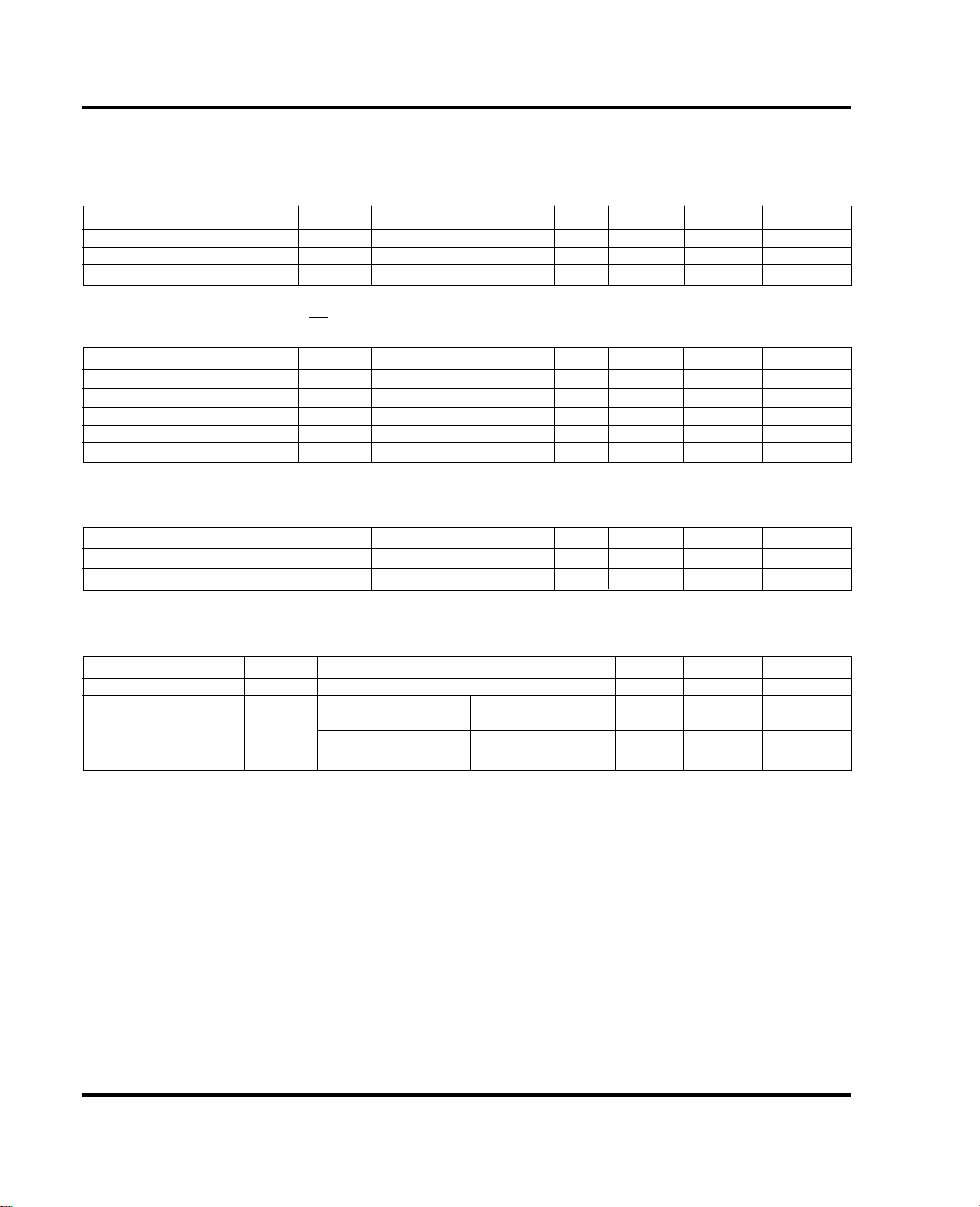
Electrical Characteristics (continued)
DD = 5.0V ±5%, V ref = 2.048V unless otherwise stated.
V
Reference Input (REFIN)
PARAMETER SYMBOL CONDITIONS MIN TYP MAX UNIT
Input voltage range VI 0VDD-2 V
Input resistance 10 MΩ
Input capacitance CI 5pF
Digital Inputs (DIN, SCLK, CS)
PARAMETER SYMBOL CONDITIONS MIN TYP MAX UNIT
High level digital input voltage VIH 2.4 V
Low level digital input voltage VIL 0.8 V
High level digital input current IIH VI = VDD ±1 µ A
Low level digital input current IIL VI = 0V ±1 µ A
Input capacitance CI 8pF
Digital Output (DOUT)
PARAMETER SYMBOL CONDITIONS MIN TYP MAX UNIT
Output voltage high V OH IO = -2mA VDD-1 V
Output voltage low VOL IO = 2mA 0.4 V
Power Supply
PARAMETER SYMBOL CONDITIONS MIN TYP MAX UNIT
Supply voltage VDD 4.5 5 5.5 V
VDD = 5.5V, no load. Vref = 0V 150 250 µA
Power supply current IDD All inputs = 0V or VDD
VDD = 5.5V, no load. Vref = 2.048V 230 350 µ A
All inputs = 0V or VDD
Wolfson Microelectronics
4
Page 5
WM5615
Electrical Characteristics (continued)
VDD = 5.0V ±5%, Vref = 2.048V unless otherwise stated.
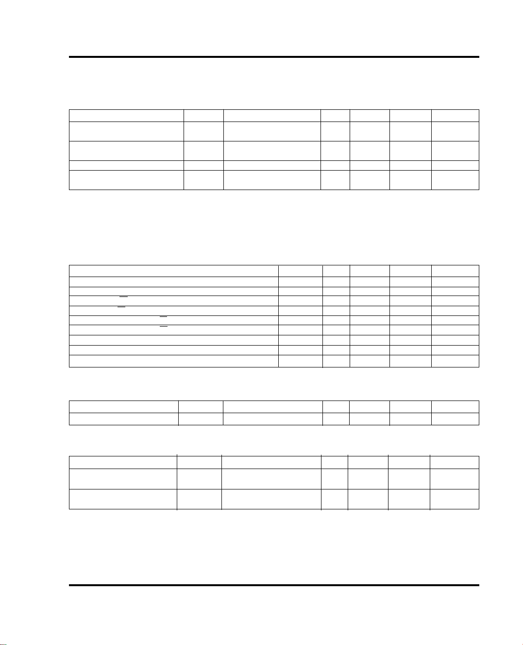
Analogue Output Dynamic Performance
PARAMETER SYMBOL CONDITIONS MIN TYP MAX UNIT
Output slew rate SR C
Output settling time tS TO 0.5 LSB CL = 100pF 12.5 µs
Glitch energy DIN = All 0s to all 1s 5 nV. s
Signal to noise + distortion S/(N+D) Vref = 2Vpp at 1kHz + 60 dB
Note 9: Settling time is the time for the output signal to remain within 0.5 LSB of the final measured value for a digital
input code change from code zero to 1023 rising and 1023 to 64 falling.
Digital Input Timing Specifications
PARAMETER SYMBOL MIN TYP MAX UNIT
Setup time, DIN before SCLK high tsu (DS) 45 ns
Hold time, DIN valid after SCLK high th (DH) 0 ns
Setup time, CS low to SCLK high tsu (CSS) 1 ns
Setup time CS high to SCLK high tsu (CS1) 50 ns
Hold time, SCLK low to CS low th (CSHO) 1 ns
Hold time, SCLK low to CS high t h (CSHI) 0 ns
Pulse duration, min. chip select pulse width height tw(CS) 20 n s
Pulse duration, SCLK low tw (CL) 18 ns
Pulse duration, SCLK high tw (CH) 18 ns
L = 100pF RL = 10 kΩ 0.3 0.5 V/µs
TA = 25oC
RL = 2kΩ (see note 9)
2.048 V DC, code 512
Output Switching Specification
PARAMETER SYMBOL CONDITIONS MIN TYP MAX UNIT
Propagation delay time tpd (DOUT) CL = 50pF 50 n s
reference input (REFIN)
PARAMETER CONDITIONS MIN TYP MAX UNIT
Reference feedthrough Input code = 00 -80 dB
(see note 10)
Reference input bandwidth Input code = 512 100 kHz
(see note 10)
Note 10: Reference feedthrough and bandwidth are measured at the DAC output with Vref input = 2Vpp at 1kHz +
2.048V DC
Wolfson Microelectronics
5
Page 6
WM5615
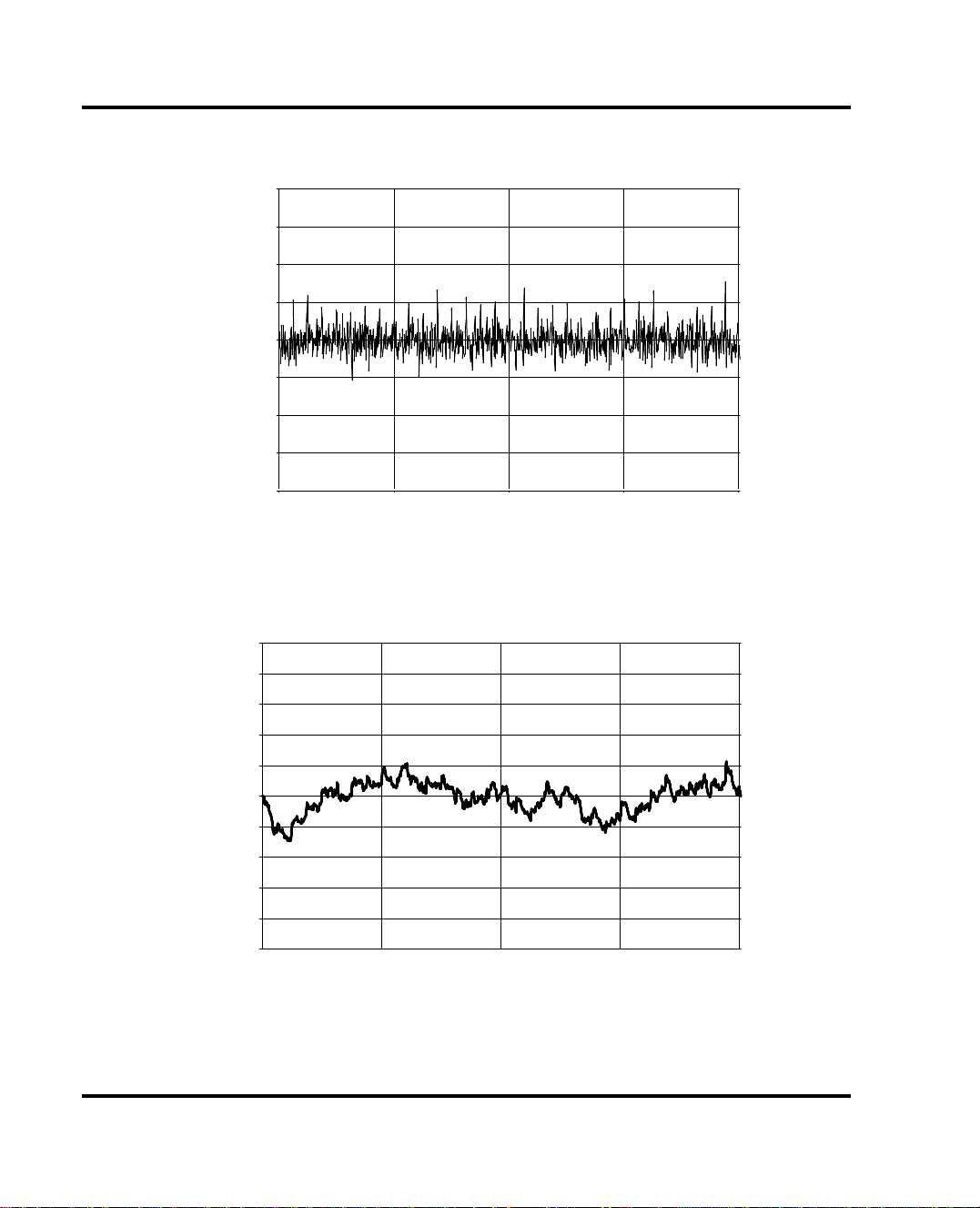
Typical Performance Characteristics
0.2
0.15
0.1
0.05
0
LSBs
LSB
-0.05
-0.1
-0.15
-0.2
1
0
256
256
WM5615 DNL Linearity Error
511
512
INPUT CODE
766
768 1024
1021
1
0.8
0.6
0.4
0.2
0
LSB
-0.2
-0.4
-0.6
-0.8
-1
1
0
256 512 768 1024
256
511
INPUT CODE
766
1021
WM5615 INL Linearity Error
Wolfson Microelectronics
6
Page 7
Pin Description
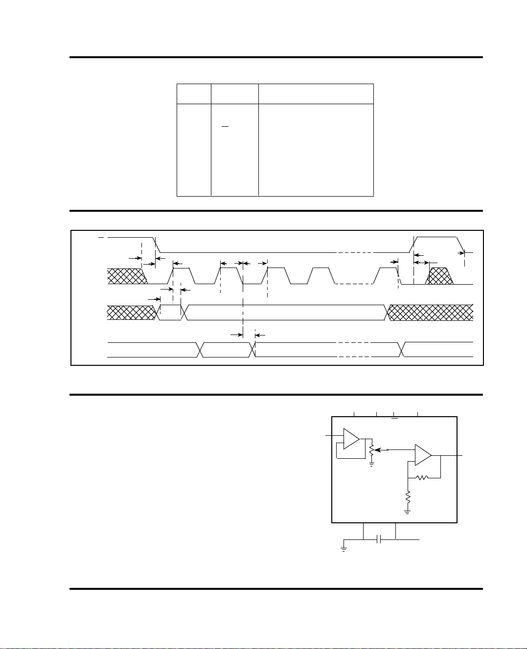
Timing Diagram
CS
th(CSHO)
SCLK
tsu(DS)
DIN
PIN NAME FUNCTION
1 DIN Serial data input.
2 SCLK Serial clock input.
3 CS Chip select, active low.
4 DOUT Serial data output for daisy-
5 AGND Analogue ground.
6 REFIN Reference input.
7 VOUT DAC output.
8 VDD Positive power supply.
tsu(CSS)
tw(CH)
th(DH)
chaining.
tw(CL)
th(CSH1)
See note C
WM5615
tw(CS)
tsu(CS1)
See note A
See note B
DOUT
NOTES: A. The input clock, applied at the SCLK terminal, should be inhibited low when CS is high to minimise clock feedthrough.
Previous LSB
B. Data input from preceeding conversion cycle.
C. Sixteenth SCLK falling edge.
tpd(DOUT)
Detailed Description
General Function
The WM5615 uses a resistor string network buffered
with a single-supply CMOS op amp in a fixed gain of x2 to
convert 10-bit digital data to analogue voltage levels (see
Block Diagram). The topology of the WM5615 makes the
output the same polarity as the reference input (see Table 1).
An internal reset circuit forces the DAC register to reset
to all 0s on power-up.
DIN SCLK
REFIN
+
-
AGND
0.1µF
Figure 1 - Typical Operating Circuit
CS
VDD
DOUT
VOUT
+
R
R
+5V
Wolfson Microelectronics
7
Page 8
WM5615
Detailed Description (Continued)
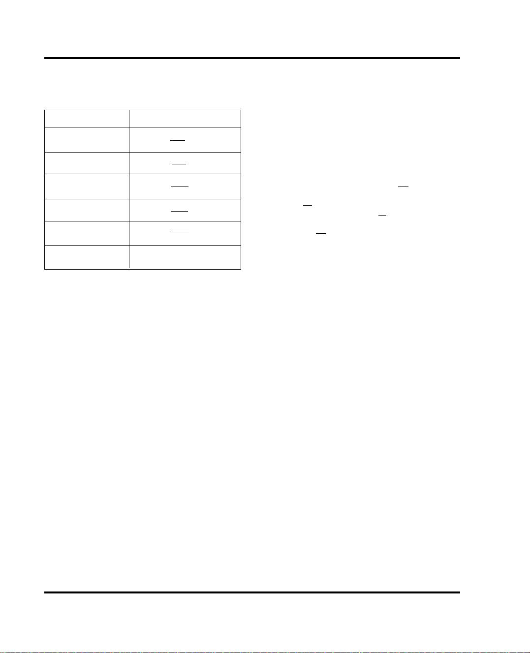
Table 1 - Binary Code Table
(0V to 2V
REFIN Output), Gain = 2
INPUT* OUTPUT
1111 1111 11 (xx) +2(V
1000 0000 01 (xx) +2(V
1000 0000 00 (xx) +2(V
0111 1111 11 (xx) +2(V
1023
)
REFIN
1024
513
)
REFIN
1024
512
) = V
REFIN
1024
511
)
REFIN
1024
REFIN
1
0000 0000 01 (xx) +2(V
0000 0000 00 (xx) 0V
* A 10-bit data word with two sub-LSB Xs must be
written since the DAC input latch is 12-bits wide.
Buffer Amplifier
The output buffer is a rail-to-rail output CMOS op amp.
Max. setting time is 12.5µs to +/-0.5 LSB of final value.
The output is short-circuit protected and can drive a 2kΩ
load with a 100pF load capacitance.
External Reference
The external voltage input is buffered and must be positive but less than V
DD - 2V. The reference voltage deter-
mines the DAC full-scale output. Since the reference
terminal is buffered, the DAC input resistance is not code
dependent and is 10MΩ minimum. The REFIN input capacitance is typically 5pF.
REFIN
)
1024
Serial Interface
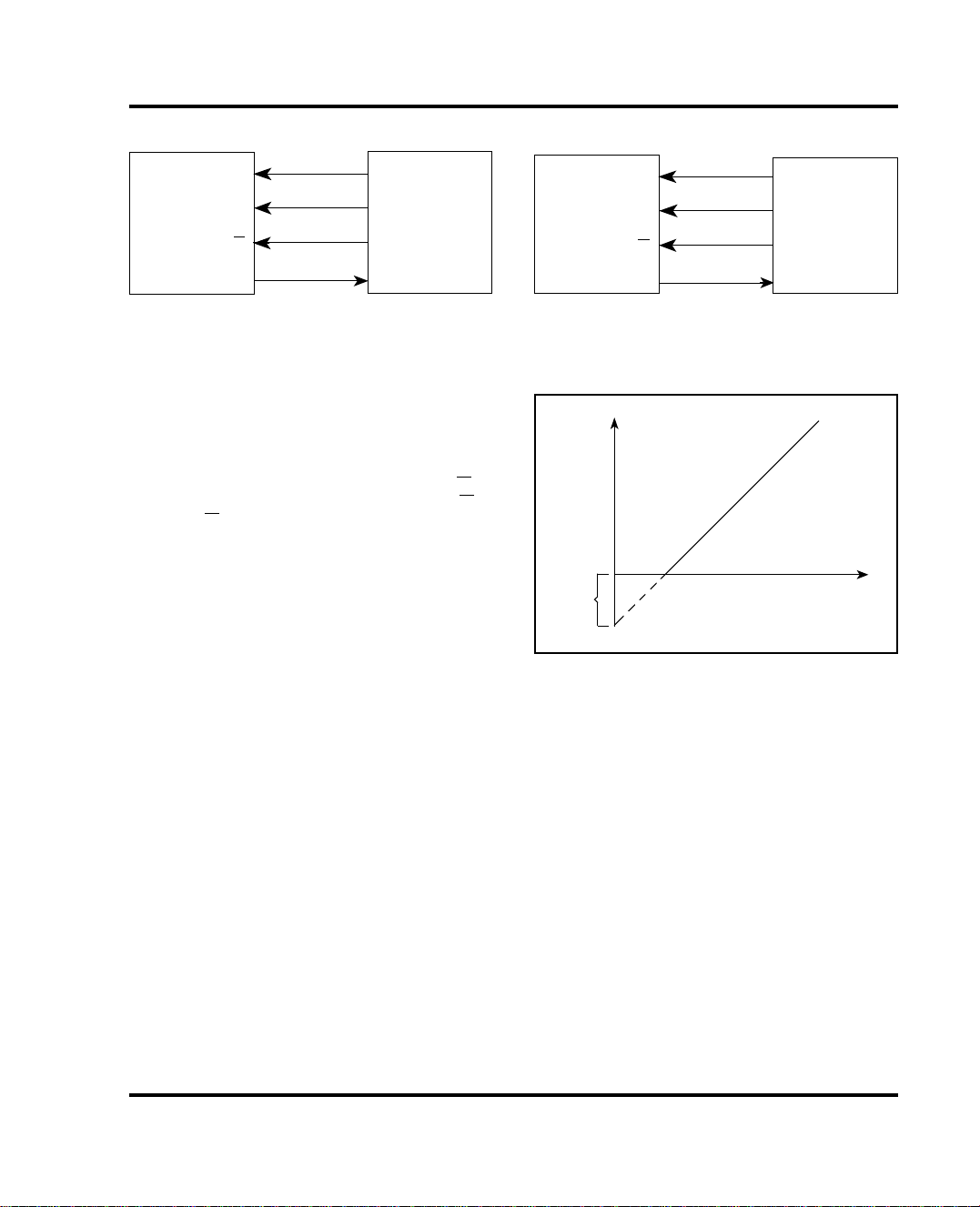
The WM5615 uses a three-wire serial interface which is
compatible with SPI, QSPI (CPOL = CPHA = 0) and
Microwire standards as shown in figures 2 and 3. The
DAC is programmed by writing two 8-bit words, MSB
first (see Block Diagram and Timing Diagram). 16 bits of
serial data are clocked into the DAC in the following order, 4 fill (dummy) bits, 10 data bits and 2 sub-LSB Xs.
The 4 dummy bits are not normally needed and are required only when DACs are daisy chained. The 2 subLSB Xs, however, are always needed because the input
register is 12 bits wide. Transitions at CS should occur
while SCLK is low. Data is clocked in on the SCLK rising
edge while CS is low . The serial input data is held in a 16bit serial shift register. On the CS rising edge, the ten
data-bits are transferred to the DAC register and update
the DAC. With CS high, data cannot be clocked into the
DIN terminal.
The WM5615 receives data in 16-bit blocks. The SPI and
Microwire interfaces output data in 8-bit blocks requiring
two write cycles to input data to the DAC. The QSPI
interface allows variable data output from 8 to 16 bits so
can load into the DAC in one write cycle.
Digital Interface
The digital inputs are designed to be compatible with TTL
or CMOS logic levels. However, to achieve the lowest
power dissipation, the digital inputs should be driven with
rail-to-rail CMOS logic. With TTL logic levels, the power
requirement increases by a factor of approximately two.
Wolfson Microelectronics
8
Page 9
Detailed Description (Continued)
WM5615
SK
SO
I/O
SI
Microwire
Port
SCLK
WM5615 SP I
DIN
CS
DOUT
SCK
MOSI
I/O
MISO
Port
WM5615
SCLK
DIN
CS
DOUT
Figure 2 - Microwire Connection Figure 3 - SPI/QSPI Connection
Note: The DOUT-MISI connection is not required for writing to the WM5615, but may be used for verifying data transfer.
Daisy-Chaining Devices
The serial output, DOUT, allows cascading of two or
more DACs. The data at DIN appears at DOUT, delayed
by 16 clock cycles plus one clock width. For low power,
DOUT does not require an external pull-up resistor. DOUT
Output
Voltage
does not go into a high-impedance state when CS is
high. DOUT changes on SCLK's falling edge when CS is
low. When CS is high, DOUT remains in the state of the
last data bit.
Any number of DACs can be daisy-chained by connecting the DOUT of one device to the DIN of the next device
in the chain.
Negative
Offset
DAC Code
Linearity, Offset and Gain Error using Single End
Supplies
When an amplifier is operated from a single supply, the
voltage offset can still be either positive or negative. With
a positive offset, the output voltage changes on the first
code change. With a negative offset, the output voltage
may not change with the first code depending on the
Figure 4 - Effect of Negative Offset (Single Supply)
This negative offset, not the linearity error, produces this
breakpoint. The transfer function would have followed
the dotted line if the output buffer could drive to a
negative voltage.
magnitude of the offset voltage.
For a DAC, linearity is measured between zero input
The output amplifier, with a negative voltage offset,
attempts to drive the output to a negative voltage.
However, because the most negative supply rail is
ground, the output cannot drive to a negative voltage. So
when the output offset voltage is negative, the output
voltage remains at zero volts until the input code value
produces a sufficient output voltage to overcome the
inherent negative offset voltage, resulting in the transfer
function shown in figure 4.
code (all inputs 0) after offset and full-scale are adjusted
out or accounted for in some way. However, single
supply operation does not allow for adjustment when
the output is negative due to the breakpoint in the
transfer function. So the linearity is measured between
the full-scale and the lowest code which produces a
positive output voltage. For the WM5615, the zero scale
(offset) is plus or minus 3LSB maximum. The code is
calculated from the maximum specification for the
negative offset.
Wolfson Microelectronics
9
Page 10
WM5615
Detailed Description (Continued)
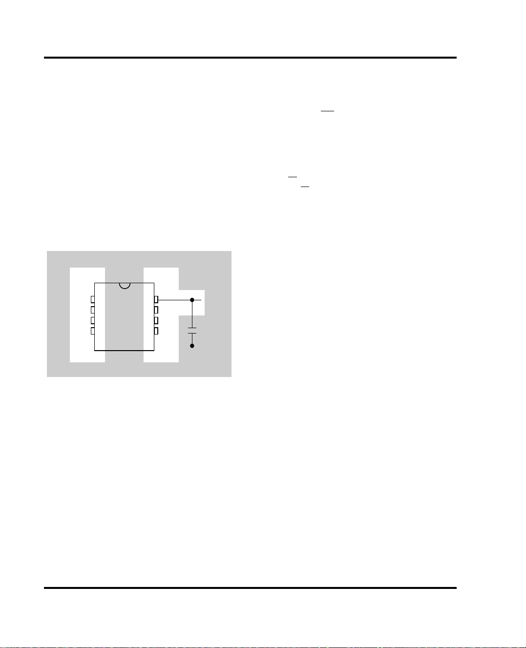
Power-Supply Bypassing and Ground Management
Best system performance is obtained with printed-circuit
boards that use separate analog and digital ground planes.
Wire-wrap boards are not recommended. The two ground
planes should be connected together at the lowimpedance power-supply source. The best ground connection may be achieved by connecting the DAC AGND
terminal to the system analogue ground plane.
DD should be bypassed with a 0.1µF ceramic capacitor
V
connected between V
with short leads close to the device. Ferrite beads may be
used to further isolate the system analogue and digital
power supplies.
Figure 5 illustrates the grounding and bypassing scheme
described.
DD and AGND. It should be mounted
Analogue Ground Plane
18
27
36
45 0.1 µF
Analogue Feedthrough
Because of internal stray capacitance, higher frequency
analog input signals may couple to the output. this is
tested by holding CS high, setting the DAC code to all 0s
and sweeping REFIN.
Digital Feedthrough
High-speed serial data at any of the digital input or output
pins may couple through the DAC package internal stray
capacitance to appear at the DAC output as noise, even
though CS is held high. This digital feedthrough is tested
by holding CS high while transmitting 1010... from DIN to
DOUT.
Figure 5 - Power-Supply Bypassing
Saving Power
When the DAC is not being used by the system, minimize
power consumption by setting the appropriate code to
minimize load. For example, with a resistive load to ground,
set the DAC code to 0 (see Table 1). In addition, the
REFIN buffer has to drive current into the DAC resistor
string and so setting REFIN to 0 further reduces power
consumption.
Wolfson Microelectronics
10
Page 11
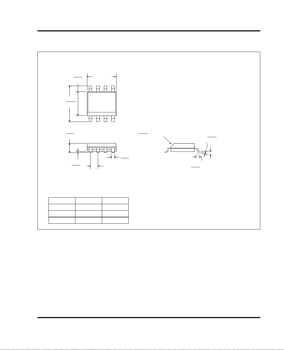
Package Descriptions
Plastic Small-Outline Package
D - 8 pins shown
WM5615
4.00
3.80
6.20
5.80
1.75
1.35
0.25
0.10
A
14
Pin spacing
1.27 B.S.C.
Dimension 'A' Variations
NMinMax
8 4.80 5.00
14 8.55 8.75
16 9.80 10.00
58
0.50
O
0.51
0.33
0.25
x 45 NOM
1.27
0.40
0.25
0.19
OO
0 to 8
Notes:
A. Dimensions in millimeters.
B. Complies with Jedec standard MS-012.
C. This drawing is subject to change without notice.
D. Body dimensions do not include mold flash or protrusion.
E. Dimension A, mould flash or protrusion shall not exceed 0.15mm. Body width, interlead flash or protrusions
shall not exceed 0.25mm.
Rev. 1 November 96
Wolfson Microelectronics
11
Page 12
WM5615
Package Descriptions
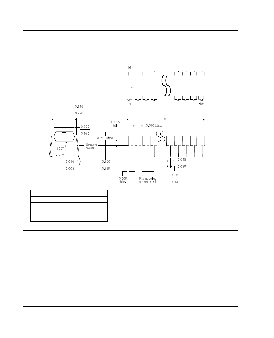
Dual-In-Line Package
N or P
0.325
0.290
0.280
0.240
105
90
O
O
0.014
0.008
Seating
plane
Dimension 'A' Variations
NMinMax
8 0.355 0.400
14 0.735 0.775
16 0.735 0.775
20 0.940 0.975
0.210 Max.
0.150
0.115
0.015
Min.
0.005
Min.
N
1
0.070 Max.
Pin spacing
0.100 B.S.C.
N/2
A
0.045
0.030
0.022
0.014
Notes:
A. Dimensions are in inches
B. Falls within JEDEC MS-001( 20 pin package is shorter than MS-001)
C. N is the maximum number of terminals
D. All end pins are partial width pins as shown, except the 14 pin package which is full
width.
Wolfson Microelectronics
12
Rev. 1 November 96
 Loading...