

Page 1
WM2630
Octal 12-bit, Serial Input, Voltage Output DAC
with Internal Reference
Production Data, Februa ry 2001, Rev 1.1
FEATURES
• Eight 12-bit DACs in one package
• Dual supply 2.7V to 5.5V operation
• DNL ±0.5 LSBs, INL ±2.0 LSBs typ.
• Programmable settling time / power
(1.0µs typ. in fast mode)
• Internal programmable Voltage Reference
• Microcontroller compatible Serial Interface
• Power Down Mode ( < 0.1µA)
• Monotonic over Temperature
• Data Output for Daisy Chaining
APPLICATIONS
• Battery powered test instruments
• Digital offset and gain adjustment
• Battery operated / remote industrial controls
• Programmable Loop Controllers
• CNC Machine Tools
• Machine and motion control devices
• Wireless telephone and communication systems
• Robotics
ORDERING INFORMATION
DEVICE TEMP. RANGE PACKAGE
WM2630CDT 0° to 70°C 20-pin TSSOP
WM2630IDT -40° to 85°C 20-pin TSSOP
DESCRIPTION
The WM2630 is an octal, 12-bit, resistor string digital-toanalogue conve rter. The eight individual DACs contained in the
IC can be switched in pairs between fast and slow (low power)
operation modes, or powered down, under software control.
Alternatively, the whole device can be powered down, reducing
current consumption to less than 0.1µA.
The DAC outputs are buffered by a rail-to-rail amplifier with a
gain of two, which is configurable as Class A (fast mode) or
Class AB (for low-power mo de).
The WM2630 has been designed to interface directly to
industry standard microprocessors and DSPs, and can
operate on two separate analogue and digital powe r supplies. It
is programmed with a 16-bit serial word comprising 4 address
bits and up to 12 DAC or control register data bits. All eight
DA Cs can be s imu lt aneous ly f or ced to a pr es et valu e us in g a
preset input pin.
A daisy-chain data output makes it possible to control several
of Wolfson’s octal DACs from the same interface, without
increasing the number of control line s.
The device is available in a 20-pin TSSOP package.
Commercial temperature (0° to 70°C) and Industrial
temperature (-40° to 85°C) variants are supported.
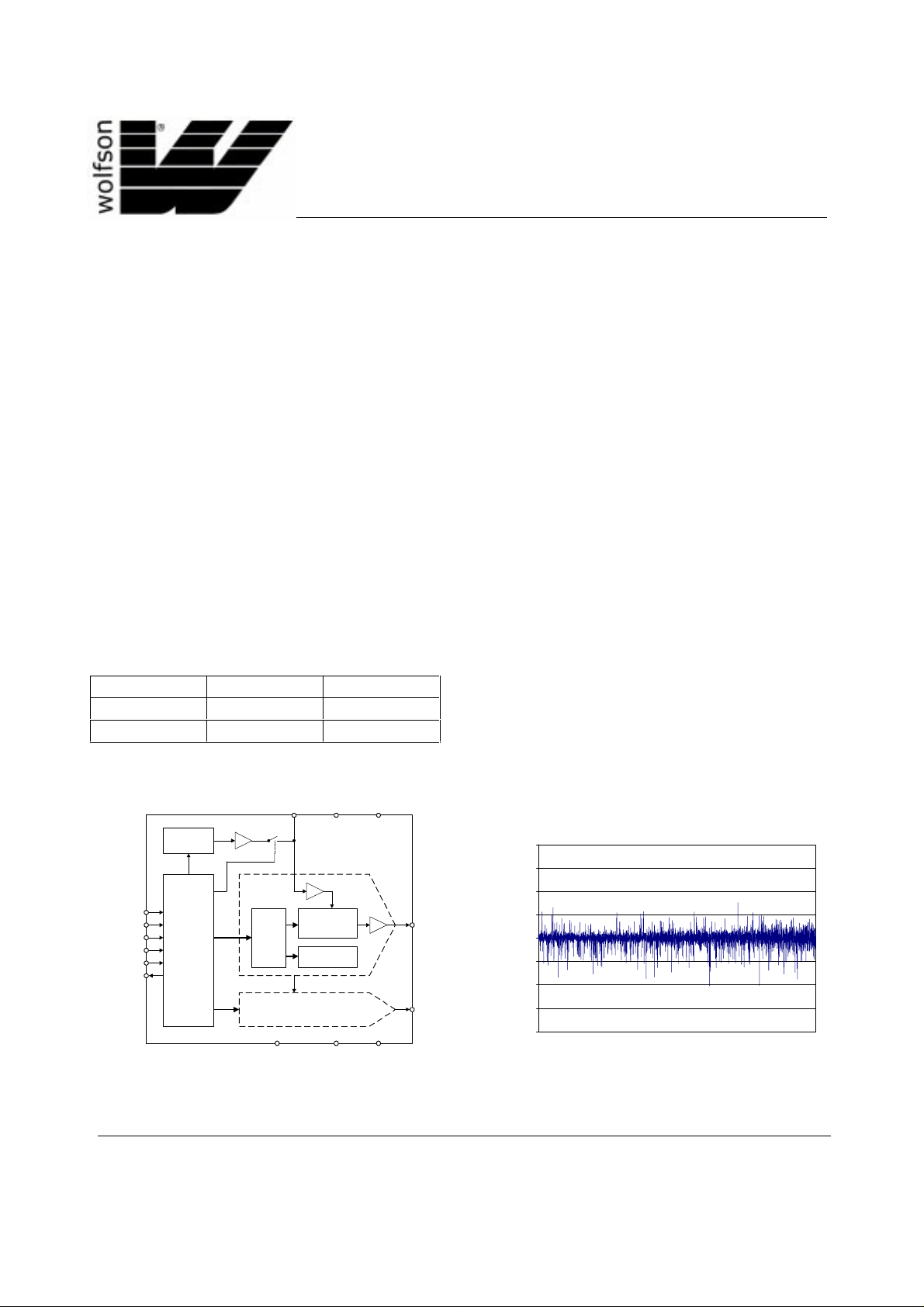
BLOCK DIAGRAM TYPICAL PERFORMANCE
REF
AVDD
(11)
AGND
(10)
DVDD
(20)
DGND
(1)
(12) OUT A
(6-9, 13-15 )
OUT B to H
1
0.75
0.5
0.25
0
-0.25
Differential N on- Li nearit y (LSBs)
-0.5
-0.75
-1
0 512 1024 1536 2048 2560 3072 3584 4096
DIGITAL CODE
Production Data datasheets contain final
specifications current on publication date.
Supply of products conforms to Wolfson
Microelectronics’ Terms and Conditions.
2001 Wolfson Microelectronics Ltd.
(16)
1.024V / 2.048V
SELECTA BLE
REFERE NCE
DAC A
DIN (2)
SCLK (3)
FS (4)
MODE (17)
PREB (5)
DOUT (19)
SERIAL
INTERFACE
AND
CONTROL
LOGIC
LATCH
DACs B, C, D, E, F, G, H
LOADB
(18)
RESISTOR
POWER/SPEED
CONTROL
REF
as DAC A
STRING
WOLFSON MICROELECTRONICS LTD
Bernard Terrace, Edinburgh, EH8 9NX, UK
Tel: +44 (0) 131 667 9386
Fax: +44 (0) 131 667 5176
Email: sales@wo lfson.co.uk
www.wolfsonmicro.co.uk
Page 2
WM2630 Production Data
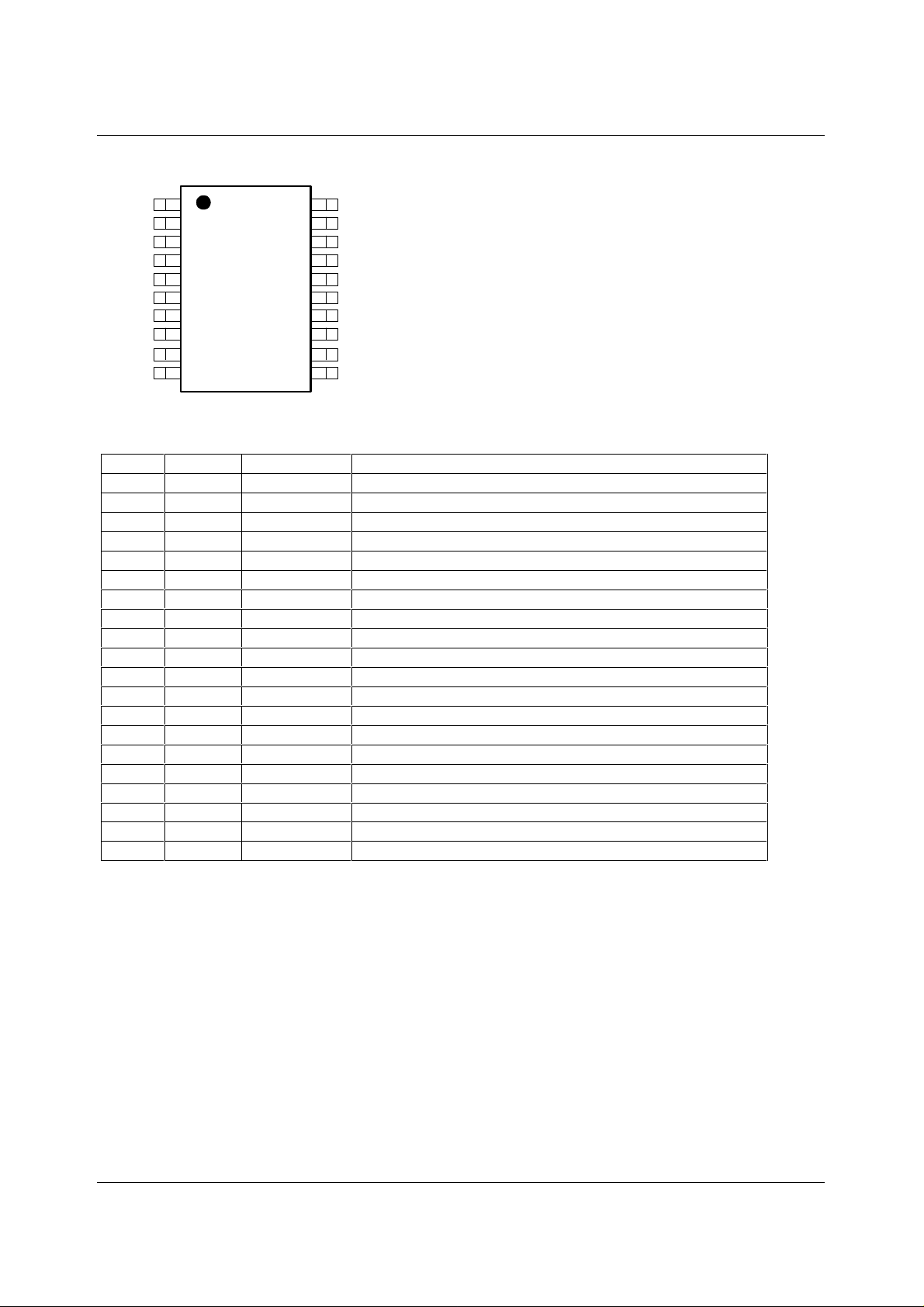
PIN CONFIGURATION
DGND
DIN
SCLK
FS
PREB
OUTE
OUTF
OUTG
OUTH
AGND
1
2
3
4
5
6
7
8
9
10
20
DVDD
19
DOUT
18
LOADB
17
MODE
16
REF
15
OUTD
14
OUTC
13
OUTB
12
11
OUTA
AVDD
PIN DESCRIPTION
PIN NO NAME TYPE DESCRIPTION
1
2
3
4
5
6
7
8
9
10
11
12
13
14
15
16
17
18
19
20
DGND Supply Digital Ground
DIN Digital input Digital serial data input
SCLK Digital input Serial clock input
FS Digital input Frame sync input
PREB Digital input Preset input
OUTE Analogue output DAC Output E
OUTF Analogue o utput DAC Output F
OUTG Analogue output DAC Output G
OUTH Analogue output DAC Output H
AGND Supply Analogue Ground
AVDD Supply Analogue positive power supply
OUTA Analogue output DAC Output A
OUTB Analogue output DAC Output B
OUTC Analogue output DAC Output C
OUTD Analogue output DAC Output D
REF Analogue I/O Voltage reference input / output
MODE Digital input Input mode
LOADB Digital input Lo ad DAC
DOUT Digital output Data serial data output
DVDD Supply Digital positive power supply
WOLFSON MICROELECTRONICS LTD PD Rev 1.1 February 2001
2
Page 3
Production Data WM2630
r
o
s
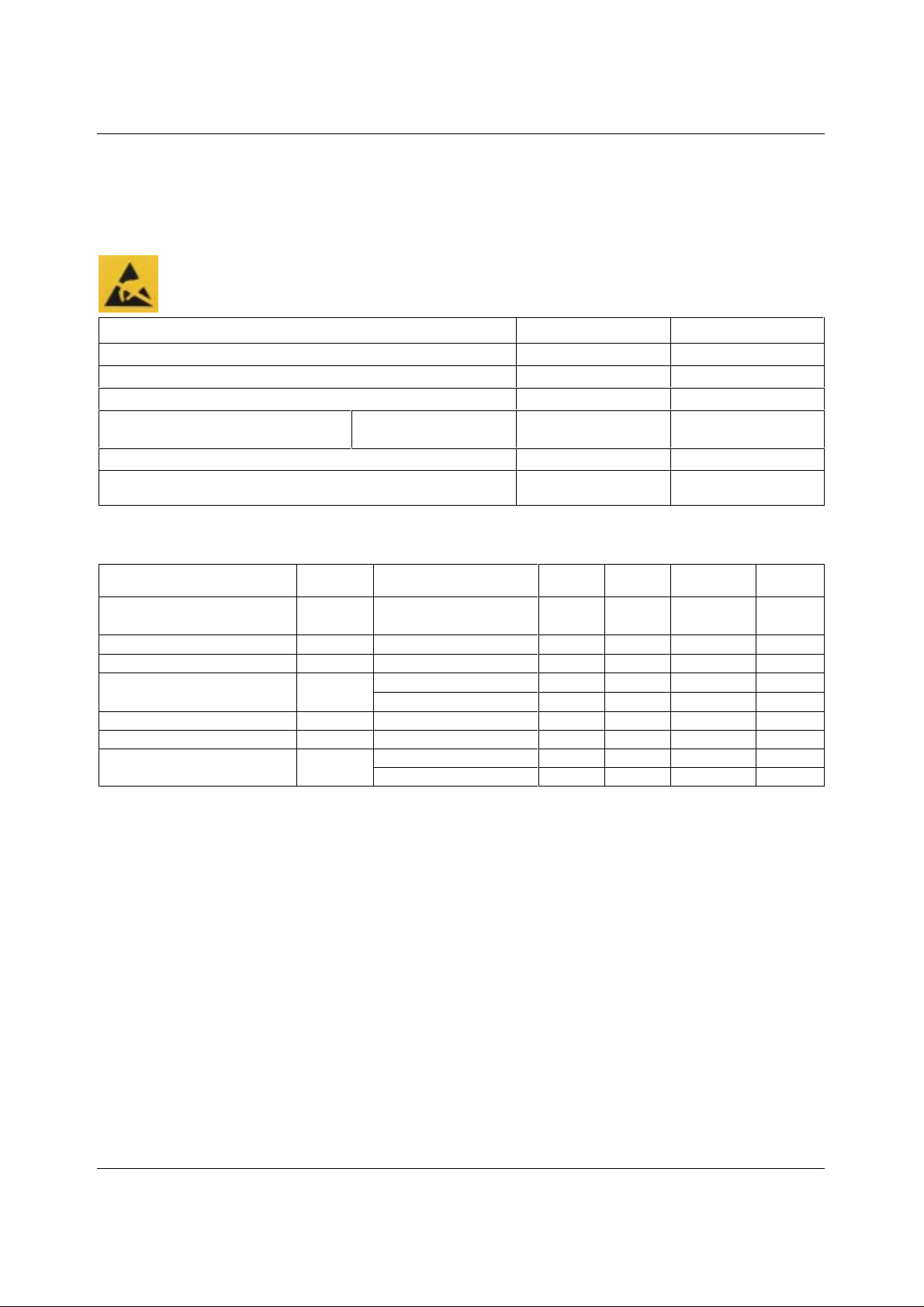
ABSOLU TE MAXIMUM RATINGS
Absolute Maximum Ratings are stress ratings on ly. Per manen t damage to the device may be caused by continuously operating at o
beyond these limits. Device functional operating limits and guaranteed performance specifications are given under Electrical
Characterist ics at the test conditio ns specified.
ESD Sen sit ive Devi ce. T his devic e is manu fac tur ed on a CM OS proc ess . It is ther efor e generically susceptible t
damage fr om exc ess i ve st atic volt ages. Proper ESD precautions must be taken during handling and storage of t hi
device.
CONDIT ION MIN MAX
Digital supply vo ltages, AVDD or DVDD to GND
Reference input voltage
Digital input voltage range to GND
Operating temperature range, T
A
WM2630CDT
WM2630IDT
Storage temperature
Soldering lead temperature, 1.6mm (1/16 inch) from package body for 10
-0.3V AVDD + 0.3V
-0.3V DVDD + 0.3V
0°C
-40°C
-65°C 150°C
7V
70°C
85°C
260°C
seconds
RECOMMENDED OPERATING CONDITIONS
PARAMETER SYMBOL TEST CONDITIONS MIN TYP MAX UNIT
Supply voltage
AVDD,
2.7 5.5 V
DVDD
High-level digital input voltage
Low-level digital input voltage
Reference voltage to REF
V
IH
V
IL
V
REF
See Note 2 V
See Note 0.8 V
AVDD = 5V GND 2.048 AVDD
AVDD = 3V GND 1.024 AVDD V
Output Load R esistance
Load capacitance
Operating free-air temperature
R
L
C
L
T
A
WM2630CDT 0 70 °C
2kΩ
100 pF
WM2630IDT -40 85 °C
Note: Reference input v oltages greater than AVDD/2 will cause saturation for large DAC codes.
WOLFSON MICROELECTRONICS LTD PD Rev 1.1 February 2001
3
Page 4
WM2630 Production Data
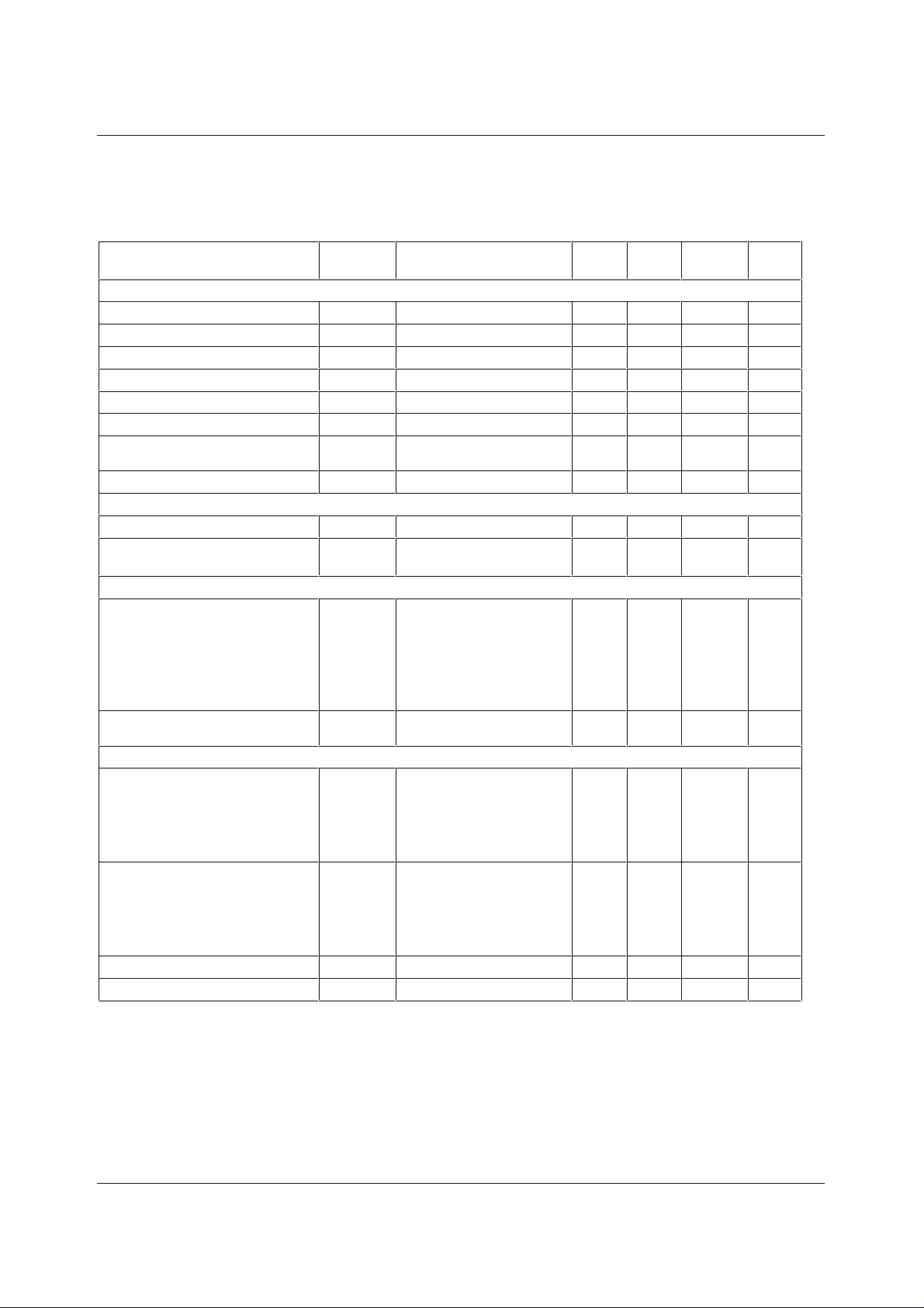
ELECTRICAL CHARACTERISTICS
Test Characteristics:
R
= 10kΩ, CL = 100pF AVDD = DVDD = 5V ± 10%, V
L
recommended operating free-air temperature range (unless noted otherwise).
= 2.048V and AVDD = DVDD = 3V ± 10%, V
REF
= 1.024V over
REF
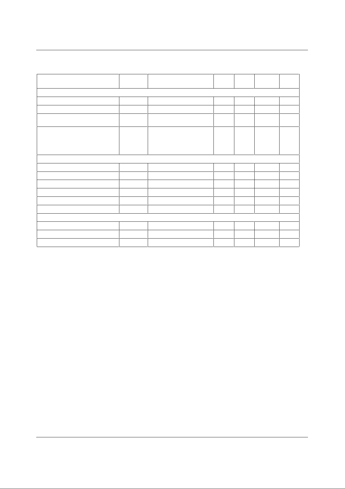
PARAMETER SYMBOL
Static DAC Specifications
Resolution
Integral non-linearity
Differential non-linea rity
Zero code error
Gain error
DC power supply rejection ratio
INL Code 40 to 4095 (see Note 1) ±2 ±6 LSB
DNL Code 40 to 4095 (see Note 2) ±0.5 ±1 LSB
ZCE See Note 3 ±30 mV
GE See Note 4 ±0.6 % FSR
PSRR See Note 5 -50 dB
Zero code error temperat ure
coefficient
Gain error temperature coefficient
DAC Output Specifications
Output voltage range
Output load regulation
Power Supplies
Active supply current
IDD No load, V
Power do wn supply current
Dynamic DAC Specifications
Slew ra te
Settling time
Glitch energy
Chann el Crosstalk
TEST
CONDITIONS
MIN TYP MAX UNIT
12 bits
See Note 6 30 µV/°C
See Note 6 10 ppm/°C
10kΩ Load 0 AVDD-0.4 V
2kΩ to 10kΩ loa d
See Note 7
=DVDD, VIL=0V
IH
±0.3 % Full
Scale
AVDD = DVDD = 5V,
V
= 2.048V
REF
Slow
Fast
16
6
21
8
mA
mA
See Note 8
No load, all inputs 0V
0.1 µA
or DVDD
DAC code 10%-90%
Load = 10kΩ, 100pF
Fast
Slow
4
1
10
V/µs
3
V/µs
See Note 9
DAC code 10%-90%
Load = 10kΩ, 100pF
Fast
Slow
1
3
3
7
µs
µs
See Note 10
Code 2047 to code 2048 4 nV-s
10kHz sine wave, 4V pk-pk -90 dB
WOLFSON MICROELECTRONICS LTD PD Rev 1.1 February 2001
4
Page 5
Production Data WM2630
Test Characteristics:
R
= 10kΩ, CL = 100pF AVDD = DVDD = 5V ± 10%, V
L
= 2.048V and AVDD = DVDD = 3V ± 10%, V
REF
= 1.024V over
REF
recommended operating free-air temperature range (unless noted otherwise).
PARAMETER SYMBOL
TEST
CONDITIONS
MIN TYP MAX UNIT
Reference Configured as Input
Reference input resistance
Reference input capacitance
Reference feedthrough
RREF 50 kΩ
CREF 10 pF
V
=2VPP at 1kHz
REF
-84 dB
+ 2.048V DC, DAC code 0
Reference input bandwidth
V
= 0.4VPP + 2.048V DC,
REF
DAC code 2048
Slow
Fast
1.9
2.2
Reference Configured as Output
Low reference vo ltage
High reference voltage
Output source current
Output sink current
Load Capacitance
PSRR
V
REFOUTL
V
REFOUTH
I
REFSRC
I
REFSNK
1.010 1.024 1.040 V
VDD > 4.75V 2.020 2.048 2.096 V
1mA
-1 mA
in parallel with 100nF cap. 1 10 µF
60 dB
Digital Inputs
High level input current
Low level input current
Input capacitance
I
IH
I
IL
C
I
Input volta ge = DVDD 1 µA
Input voltag e = 0V -1 µA
8pF
Notes:
1. Integral non-linearity (INL) is the maximum deviation of the o utput from the line between zero and full scale excluding the
effects of zero code a nd full scale er rors).
2. Differential non-linearity (DNL) is the difference betwee n the measured a nd ideal 1LSB amplitude change
of any adjacent two codes. A guarantee of monotonicity means the output voltage changes in the same
direction (or remains constant) as a change in digital input code.
3. Zero code error is the voltage output when the DAC input code is zero.
4. Gain error is the deviation from the ideal full-scale output excluding the effects of zero code error.
5. Power supply rejection ratio is measured by varying AVDD from 4.5V to 5.5V and measuring the
proportion of this signal imposed on the zero code error and the gain error.
6. Zero code error and Gain error temperature coefficients are normalised to full-scale voltage.
7. Output load regulation is the difference between the output voltage at full scale with a 10kΩ load and 2kΩ
load. It is expressed as a percentage of the full scale output voltage with a 10kΩ load.
is measured while continuously writing code 2048 to the DAC. For VIH < DVDD - 0.7V and VIL > 0.7V
8. I
DD
supply current will increase.
9. Slew rate results are for the lower value of the rising and falling edge slew rates.
10. Settling time is the time taken for the signal to settle to within 0.5LSB of the final measured value for both rising and falling
edges. Limits are ensured by design and characterisation, but are not production tested.
MHz
MHz
WOLFSON MICROELECTRONICS LTD PD Rev 1.1 February 2001
5
Page 6
WM2630 Production Data
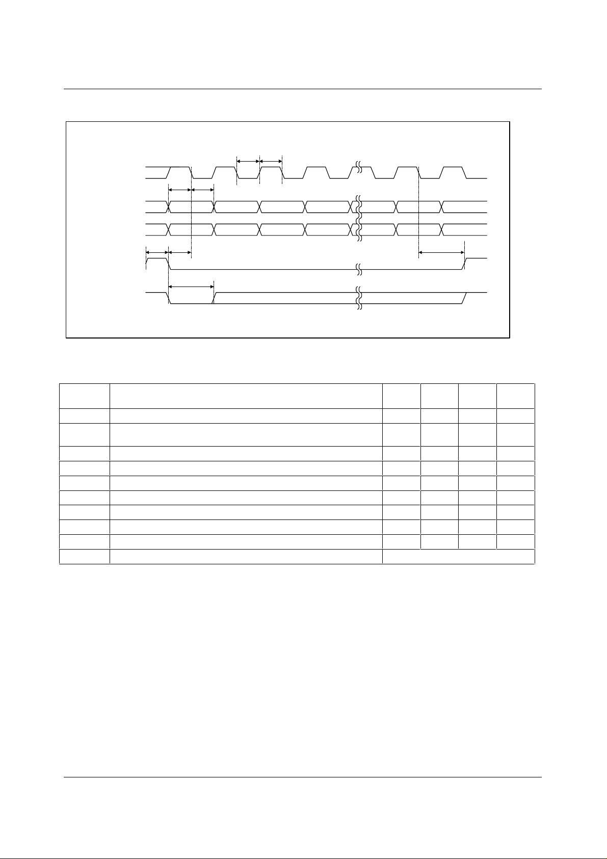
SERIAL INTERFACE
t
t
WL
WH
SCLK
DIN
DOUT
FS
µ
C MODE)
(
FS
(DSP MODE)
X1234 16 X
t
SUD
t
HD
XD15 D14 D13
XD15 * D14 * D13 * D12 * D1 * D0 * X
t
WHFStSUFSCLK
* DIN data from previous word
(delayed by 16 clock cycles)
t
WLFS
No high to low transitions
Figure 1 Timing Diagram
SYMBOL TEST
CONDITIONS
t
SUFSCLK
t
C16-FS
Setup time, FS pin low before first falling edge of SCLK
Setup time, 16th falling clock edge after FS low to rising edge of FS (only
used in microcontroller mode)
t
WLOADB
t
WH
t
WL
t
SUD
t
HD
t
WHFS
t
WLFS
t
s
Pulse duration, LOADB low
Pulse duration, SCLK high
Pulse duration, SCLK low
Setup time, data ready be fore SCLK falling edge
Hold time, data held valid after SCLK falling edge
Pulse duration, FS high
Pulse duration, FS low
DAC Output settling time
2
D1 D0 X
t
SUC16-FS
MIN TYP MAX UNIT
8ns
10 ns
10 ns
16 ns
16 ns
8ns
5ns
10 ns
10 ns
see Dyna mic DAC Specifications
WOLFSON MICROELECTRONICS LTD PD Rev 1.1 February 2001
6
Page 7
Production Data WM2630
)
Figure
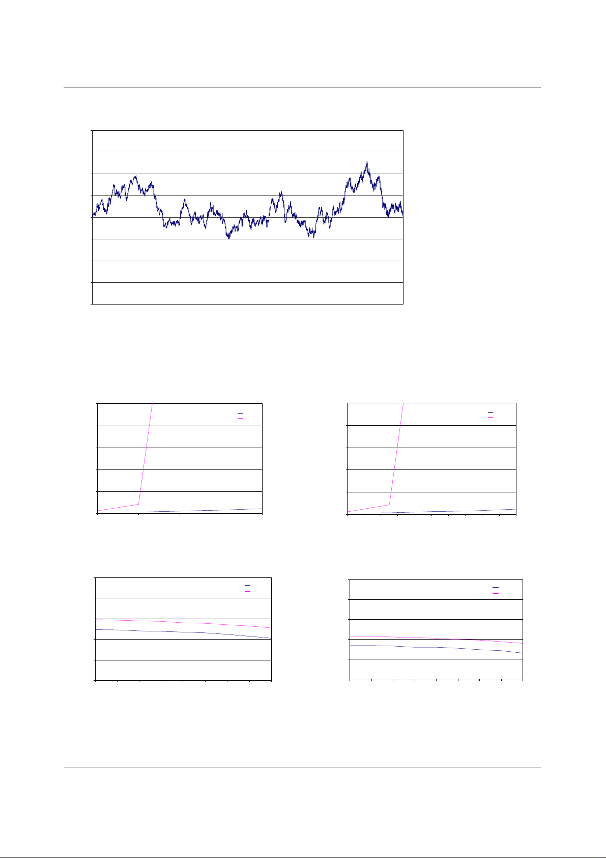
TYPICAL PERFORMANCE GRAPHS
4
3
2
1
0
-1
-2
Integral Non-Li nearity (LSBs)
-3
-4
0 512 1024 1536 2048 2560 3072 3584 4096
DIGITAL CODE
Figure 2 Integral Non-Linearity
1
VDD = 3.3V
V
= 1.024V
REF
Input Code = 0
0.8
0.6
0.4
Output Voltage (V)
0.2
0
00.511.52
Sink Current (mA)
Slow
Fast
1
VDD = 5V
= 2.048V
V
REF
Input Code = 0
0.8
0.6
0.4
Output Voltage (V
0.2
0
00.20.40.60.811.21.41.61.82
Sink Current (mA)
Slow
Fast
Figure 3 Output Load Regulation (Sink) AVDD = 3V Figure 4 Output Load Regulation (Sink) AVDD = 5V
2.1
2.08
2.06
2.04
DACA (Volts)
2.02
2
VDD=3V
V
=1.024V
REF
Input Code = 4095
Sourcing Current (mA)
Slow
Fast
-4-3.5-3-2.5-2-1.5-1-0.50
4.15
4.13
4.11
4.09
DACA (Volts)
4.07
4.05
VDD=5V
V
=2.048V
REF
Inpu t Code = 4095
Sourcing Current (mA)
Slow
Fast
-4-3.5-3-2.5-2-1.5-1-0.50
Figure 5 Output Load Regulation (Source) AVDD = 3V
6 Output Load Regulation (Source) AVDD = 5V
WOLFSON MICROELECTRONICS LTD PD Rev 1.1 February 2001
7
Page 8
WM2630 Production Data
DEVICE DESCRIPTION
GE NERAL FUNCTION
The W M2630 is an octal 12-bit, voltage output DAC. It contains a s erial interface, c ontrol logic f or speed
and power down, a programmable voltage reference, and eight digital to analogue converters. Each
converter uses a resistor s tring network buff ered with an op amp to convert 12-bit digital data to analogue
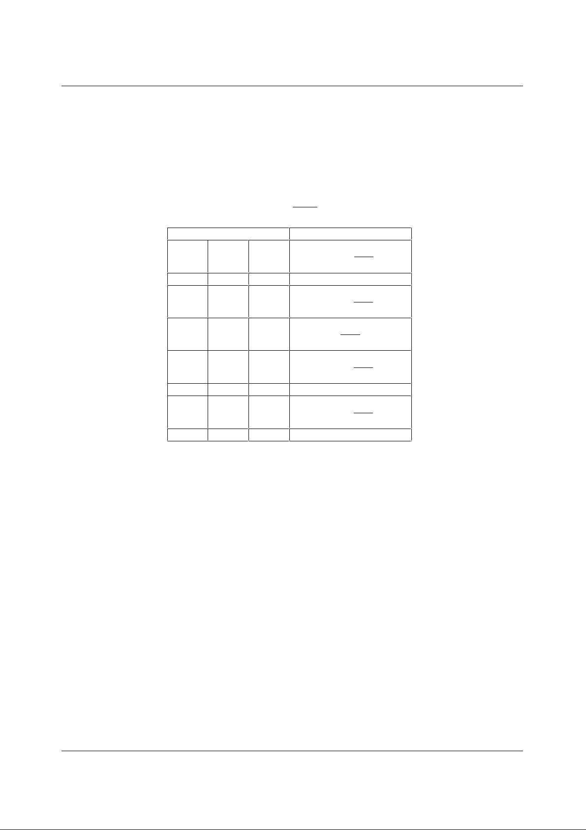
voltage levels (see Block Diagram). The output voltage is determined by the reference input voltage and
the input code a ccording to the following rela tionship:
Output voltage =
INPUT OUTPUT
1111 1111 1111
::
1000 0000 0001
1000 0000 0000
0111 1111 1111
::
0000 0000 0001
0000 0000 0000 0V
Table 1 Binary Code Table (0V to 2V
CODE
()
REF
V2
4096
Output), Gain = 2
REF
4095
()
REF
V2
4096
2049
V2
()
REF
4096
2048
()
V2 =
4096
2047
()
REF
V2
4096
()
REF
V2
4096
REFREF V
1
POWER ON RESET
An internal p ower-o n -reset circuit resets the DAC register to all 0s on power-up.
BUFFER AMPLIFIER
The output buffer has a near rail-to-rail output with short circuit protection and can reliably drive a 2kΩ
load with a 100pF load capa citance.
PROGRAMMABLE REFERENCE
The DAC reference can be sourced internally or ex ternally under software control. If an external reference
voltage is applied to the REF pin, the device must be configured to accept this . If an internal reference is
selected, a voltage of 1.024V or 2.048 is available. The internal reference can source up to 1mA and c an
therefore be used as an external system reference.
WOLFSON MICROELECTRONICS LTD PD Rev 1.1 February 2001
8
Page 9
Production Data WM2630
SER IAL INTERFACE
INTERFACE M ODES
The control interface can operate in two different modes:
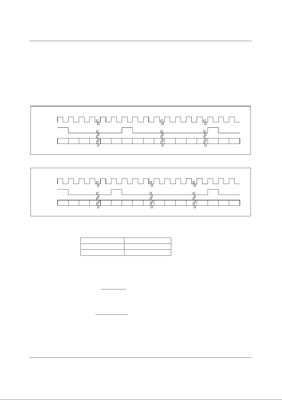
• In the microcontroller mode, FS needs to be held low until all 16 data bits have been transferred. If
FS is driven high before the 16
updated a fter a rising edge on FS.
• In DSP mode, FS only needs to stay low for 20ns, and can go high before the 16
SCLK
FS
DIN
Figure 7 Interface Timing in Microcontroller Mode
SCLK
FS
DIN
X
D15 D14 D1 D0 X E15 E14 E1 E0 X F15 F14X
X
D15 D14 D1 D0 E15 E14 E0 X X F15 F14X
th
falling clock edge, the data transfer is cancelled. The DAC is
th
falling clock edge.
E1
Figure 8 Interface Timing in DSP Mode
The operating mode is selected using pin 17 (MODE).
MODE PIN (17) INTERFACE MODE
LOW or unconnected DSP mode
Table 2 Interface Mode Selection
SERIAL CLOCK AND UPDATE RATE
Figure 1 shows the interface timing. The maximum serial clock rate is:
f
SCLK
max
Since a da ta word contains 16 bits, the sample rate is limited to
f
=
s
max
16
However, the DAC settling time to 12 bits accuracy limits the response time of the analogue output for
large input step transitions.
HIGH Microcontroller
=
1
tt
+
WLWH
minmin
1
tt
+
()
WLWH
minmin
MHz
31
=
MHz
95.1
=
WOLFSON MICROELECTRONICS LTD PD Rev 1.1 February 2001
9
Page 10
WM2630 Production Data
DAISY CHAINING MULTIPLE DEVICES
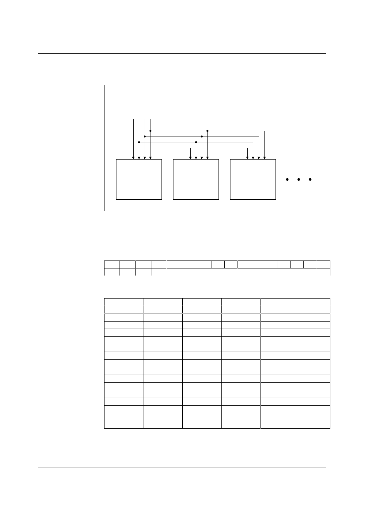
The DOUT output (pin 19) pr ovides the data sampled on DIN with a delay of 16 clock cycles. This s ignal
can be used to control another WM2630 or similar device in a daisy-chain type circuit.
DIN
SCLK
LOADB
FS
FS
DIN
SCLK
DOUT
LOADB
OCTAL DAC #1
Figure 9 Daisy Chaining
SOFTWARE CONFIGURATION OPTIONS
DATA FORM AT
The WM2630 is controlled with a 16-bit code consisting of four address bits, A0-A3, and 12 data bits.
D15 D14 D13 D12 D11 D10 D9 D8 D7 D6 D5 D4 D3 D2 D1 D0
A3 A2 A1 A0 Data
Table 3 Input Data Format
Using the four address bits, 16 different registers can be addressed.
A3 A2 A1 A0 REGISTER
0 0 0 0 DAC A Code
0 0 0 1 DAC B Code
0 0 1 0 DAC C Code
0 0 1 1 DAC D Code
0 1 0 0 DAC E Code
0 1 0 1 DAC F Code
0 1 1 0 DAC G Code
0 1 1 1 DAC H Code
1 0 0 0 Control Register 0
1 0 0 1 Control Register 1
1 0 1 0 Preset all DACs
1 0 1 1 RESERVED
1 1 0 0 DAC A and complement B
1 1 0 1 DAC C and complem ent D
1 1 1 0 DAC E and complement F
1 1 1 1 DAC G and complement H
Table 4 Register Map
FS
DIN
SCLK
LOADB
OCTAL DAC #2
FS
DIN
DOUT
OCTAL DAC #3
SCLK
LOADB
DOUT
WOLFSON MICROELECTRONICS LTD PD Rev 1.1 February 2001
10
Page 11
Production Data WM2630
DAC A TO H CODE REG ISTERS
Addresses 0 to 7 are the DAC registers. The data written to these registers is transferred to the
respective DAC when the LOADB input ( pin 18) is low. For instantaneous updating, LOADB can be held
low permanently.
CONTROL REG ISTER 0
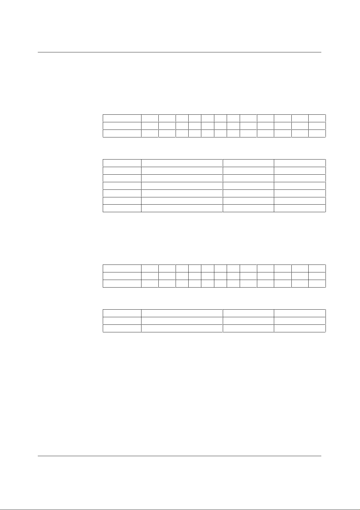
Control register 0 (address 8) is used to select functions that apply to the whole IC, such as Power Down
and Data Input Fo rmat.
BIT D11D10D9D8D7D6D5D4D3D2D1D0
Function X X XXXXXPDDOR1 R0 IM
Default XXXXXXX00000
Table 5 Register Map
BIT DESCRIPTION 0 1
PD Full device Power Down Normal Power Down
DO DOUT Enable Disable d Enabled
R1 Int / Ext Reference Select External Internal
R0 Internal Reference Select 1.024V 2.048V
IM Input Mode Straight Binary Two’s Complement
X Reserved
Table 6 Register Map
CONTROL REG ISTER 1
Control register 1 (address 9) is used to power down individual pairs of DACs and select their settling
time. Powering down a pair of DAC s dis ables their amplifiers and reduces the power consumption of the
device. The settling time in fast mode is typically 1µs. In slow mode, the settling time is typically 3µs and
power consumption is reduced.
BIT D11D10D9D8D7D6D5D4D3D2D1D0
Function X X X X PGHPEFPCDP
S
S
S
AB
GH
EF
S
CD
Default XXXX00000000
Table 7 Register Map
BIT DESCRIPTION 0 1
P
XY
S
XY
Power Down DACs X and Y Normal Powe r Down
Speed Setting for DACs X and Y Slow Fast
Table 8 Register Map
DAC PRESET REGISTER
The Preset register (address 10) makes it possible to update all eight DACs at t he s ame time. T he value
stored in this register becomes the digital input to all the DACs when the asynchronous PREB input (pin
5) is driven low. If no data has previously been written to the preset register, all DACs are set to zero
scale.
TWO-CHANNEL REGISTERS
The two-channel registers (addresses 12 to 15) provide a ‘differential output’ function where writing data
to one DAC will automatically write the complement to the other DAC in the pair. For example, writing a
hexadecimal v alue of FFFF to address 12 will set DAC A to full scale and DAC B to zero scale.
AB
WOLFSON MICROELECTRONICS LTD PD Rev 1.1 February 2001
11
Page 12
WM2630 Production Data
PROGRAMMABLE INTERNAL REFERENCE
The reference can be sourced internally or externally under software control. If an external reference
voltage is applied to the REF pin, the device must be configured to accept this.
If an external reference is selected, the reference voltage input is buff ered which makes the DAC input
resistance independent of code. The REF pin has an input resistance of 10MΩ and an input capacitance
of typically 55pF. The refere nce voltage determines the DAC full-scale output.
If an internal reference is selected, a voltage of 1.024V or 2.048 is available. The internal reference can
source up to 1mA and can therefore be used as an external system reference.
REF1 REF0 REFERENCCE
0 0 External (default)
0 1 1.024V
1 0 2.048V
11 External
Table 9 Programmable Internal Reference
APPLICATIONS INFORMATION
LINEARITY, OFFSET, AND GAIN ERROR
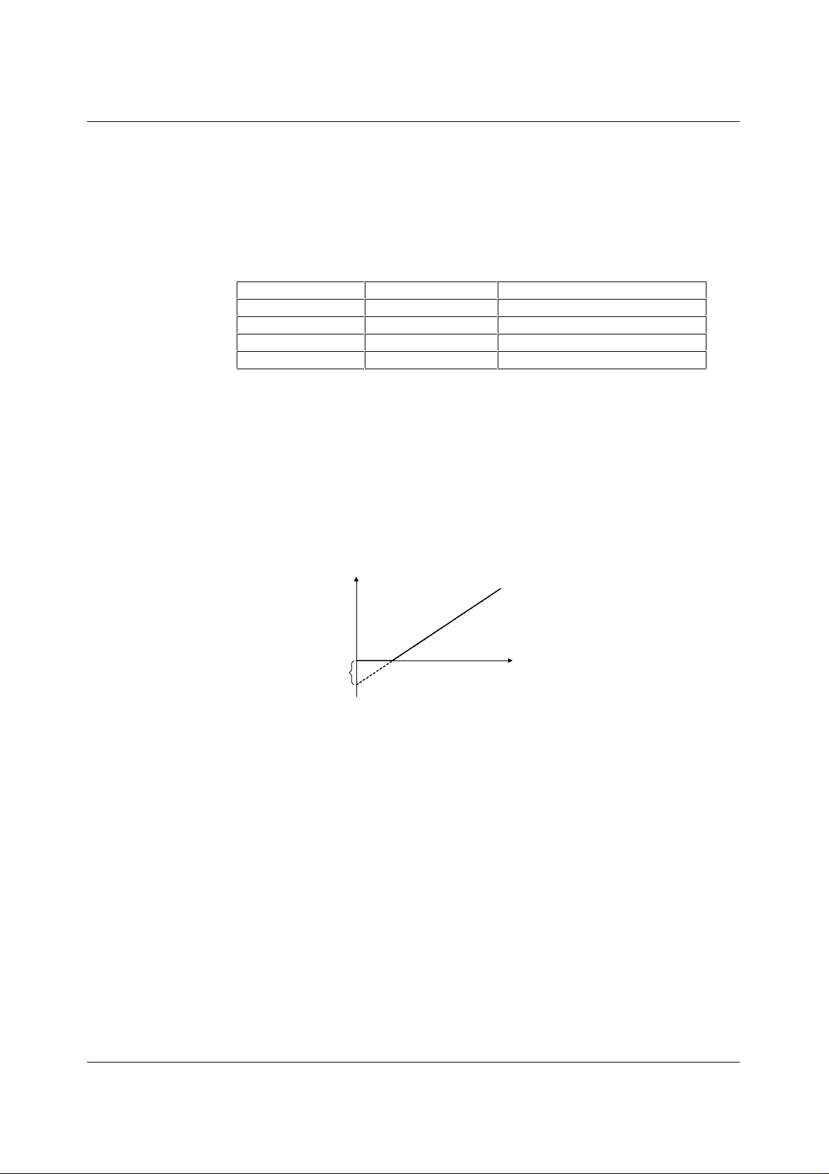
Amplifiers operating from a single supply can have positive or negative voltage offs ets. W ith a positive
offset, the output voltage changes on the first code transition. Ho wever, if the offset is negative, the output
voltage may not change with the first code, depending on the magnitude of the offs et voltage. This is
because with the most negative supply rail being ground, any attempt to drive the output amplifier below
ground will clamp the output at 0 V. The output voltage then remains at zero until the input code is
su ff ic i en t ly hig h to overc om e t he neg at i ve offs et voltag e, res u l tin g i n th e t ransf er f u n ct i on show n i n Fi g u re
10.
Output
Voltage
0 V
Negative
Offset
Figure 10 Effect of Negative Offset
This off set error, not the linearity error, produces the breakpoint. The transf er func tion would follow the
dotted line if the output buffer could drive below the ground rail.
DAC linearity is measured between zero-input code (all input bits at 0) and full-scale code (all inputs at 1),
disregarding offset and full-s cale errors. However, due to the breakpoint in the transfer function, single
supply operation does not allow for adjustment when the offset is negative. In such c ases, the linearity is
ther efore m easured between f ull -sc ale and th e lowest code th at prod uces a posit ive (non- zero) output
voltag e.
DAC code
POWER SUPPLY DECO UPLING AND GROUNDING
Printed circuit boards with separate analogue and digital ground planes deliver the best system
performance. The two ground planes should be connected together at the low impedance power supply
source. Ground currents should be managed so as to minimise voltage drops across the ground planes.
A 0.1µF decoupling capacitor should be connected between the positive supply and ground pins of the
DA C, wi th s hort leads as c lose as pos sib le to t he devi ce. Us e of fer rit e beads may fur ther is olate the
system analogue supply from the digital supply.
WOLFSON MICROELECTRONICS LTD PD Rev 1.1 February 2001
12
Page 13
Production Data WM2630
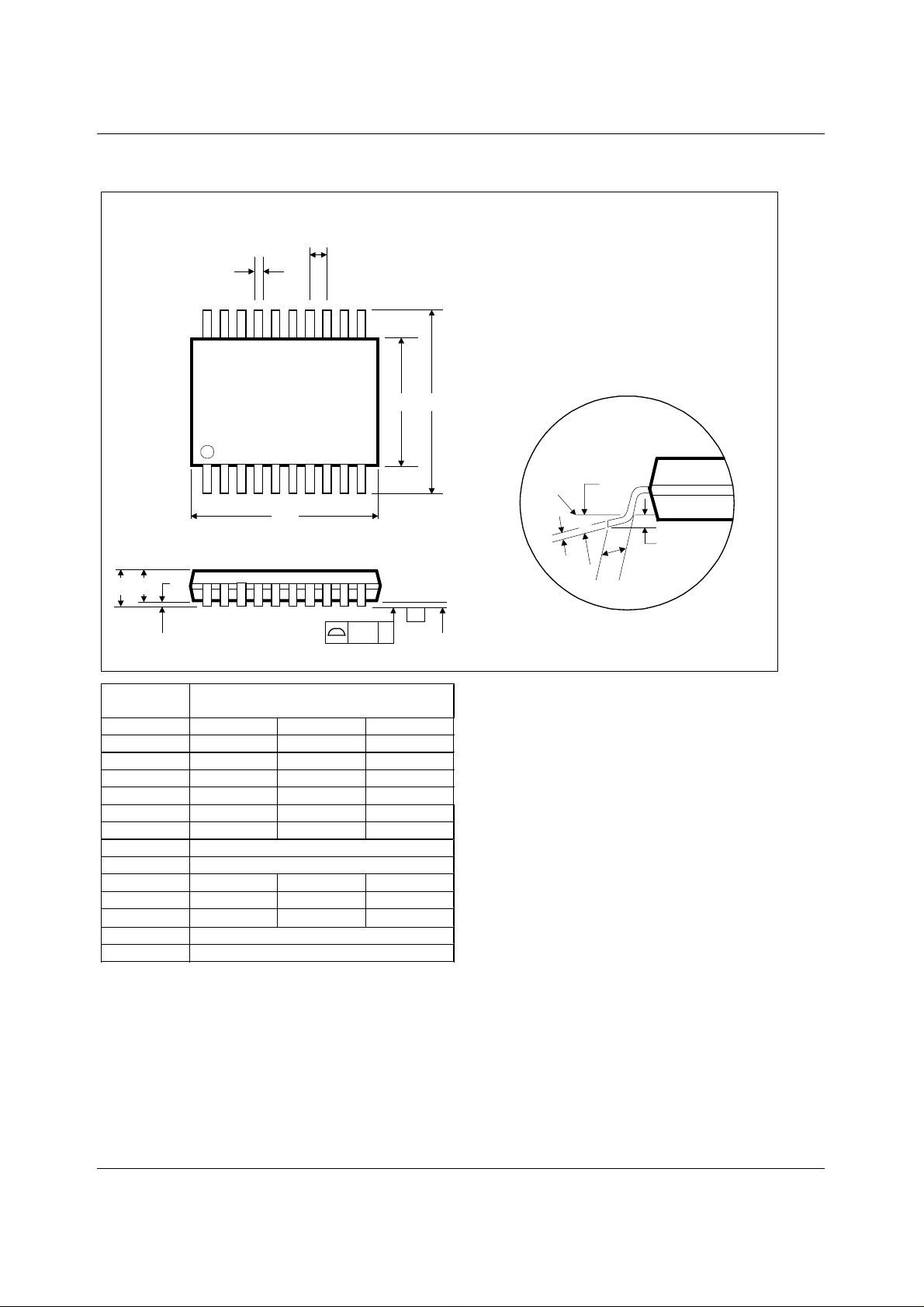
PACKAGE DIMENSIONS
DT: 20 PIN TSSOP (6.5 x 4.4 x 1.0 mm)
b
A1
A2
A
e
1120
D
101
0.1 C
E1 E
-C-
SEAT I NG PL ANE
GAUGE
PLANE
DM008.D
θ
0.25
c
L
Dimensions
Symbols
(mm)
MIN NOM MAX
A
A
1
A
2
b
c
D
e
E
E
1
L 0.45 0.60 0.75
θ
REF:
NOTES:
A. ALL LINEAR DIMENSIONS ARE IN MILLIMETERS.
B. THIS DRAWING IS SUBJECT TO CHANGE WITHOUT NOTICE.
C. BODY DIMENSI ONS DO NOT INCLUDE MOLD FLASH OR PROTRUSION, NOT TO EXCEED 0.25MM .
D. MEETS JEDEC.95 MO-153, VARIATION = AC. REFER TO THIS SPECIFICATION FOR FURTHER DETAILS.
----- ----- 1.20
0.05 ----- 0.15
0.80 1.00 1.05
0.19 ----- 0.30
0.09 ----- 0.20
6.40 6.50 6.60
0.65 BSC
6.4 BSC
4.30 4.40 4.50
o
0
----- 8
o
JEDEC.95, MO-153
WOLFSON MICROELECTRONICS LTD PD Rev 1.1 February 2001
13
 Loading...