

Page 1
WM2604
DNL (LSB)
Quad 10-Bit Serial Input Voltage Output DAC
Production Data, June 1999, Rev 1.0
FEATURES
• Four 10-bit voltage output DACs
• Dual 2.7V to 5.5V supply (separate digital and analogue
supplies)
• DNL ±±0.1 LSB, INL ±±0.4 LSB
• Low power consumption:
- 5.5mW, slow mode - 5V supply
- 3.3mW, slow mode - 3V supply
• TMS320, (Q)SPI, and Microwire compatible serial
interface
• Programmable settling time of 4µµs or 12µµs typical
APPLICATIONS
• Battery powered test instruments
• Digital offset and gain adjustment
• Battery operated/remote industrial controls
• Machine and motion control devices
• Wireless telephone and communication systems
• Speech synthesis
• Arbitrary waveform generation
ORDERING INFORMATION
DEVICE TEMP. RANGE PACKAGE
WM2604CDT 0° to 70°C 16-pin TSSOP
WM2604IDT -40° to 85°C 16-pin TSSOP
DESCRIPTION
The WM2604 is a quadruple 10-bit voltage output, resistor string,
digital-to-analogue converter. Each DAC can be individually
powered down under software control. A hardware controlled mode
is provided that powers down all DACs. Power down reduces
current consumption to 10nA.
The device has been designed to interface efficiently to industry
standard microprocessors and DSPs, including the TMS320
family. The WM2604 is programmed with a 16-bit serial word
comprising of a DAC address, individual DAC control bits and a
10-bit value.
The WM2604 has provision for two supplies: one supply for the
serial interface (DVDD, DGND), and one for the DACs, reference
buffers and output buffers (AVDD, AGND). This enables a typical
application where the device can be controlled via a
microprocessor operating on a 3V supply, with the DACs operating
on a 5V supply. Alternatively, the supplies can be tied together in a
single supply application.
Excellent performance is delivered with a typical DNL of ±0.1 LSB.
The settling time of the DAC is programmable to allow the designer
to optimize speed versus power dissipation. The output stage is
buffered by a x2 gain near rail-to-rail amplifier, which features a
Class AB output stage. DACs A and B can have a different
reference voltage to DACs C and D.
The device is available in a 16-pin TSSOP package. Commercial
temperature (0° to 70°C) and Industrial temperature (-40° to 85°C)
variants are supported.
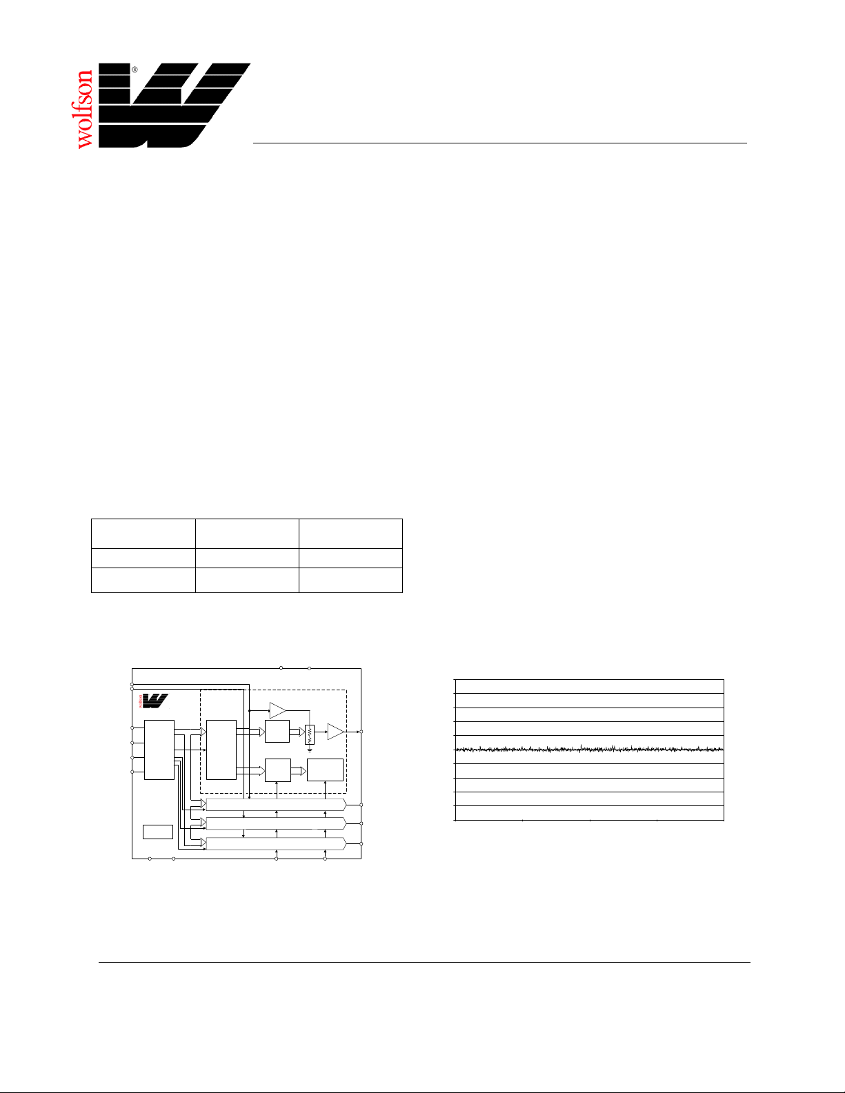
BLOCK DIAGRAM TYPICAL PERFORMANCE
AVDD
DVDD
(16)
(1)
REFINAB (15)
REFINCD (10)
DIN (4)
FS (7)
SCLK (5)
NCS (6)
WM2604
16-BIT
SHIFT
REGISTER
CONTROL
LOGIC
POWER-ON
RESET
(9)
AGND
DAC A
data
12-BIT
DATA AND
AND
DGND
CONTROL
HOLDING
LATCH
(8)
REFERENCE
INPUT BUFFER
X1
10-BIT
DAC
LATCH
2-BIT
CONTROL
LATCH
DAC B
DAC C
DAC D
(3)
NLDAC
OUTPUT
BUFFER
POWERDOWN/
SPEED
CONTROL
(2)
NPD
DAC
X2
WOLFSON MICROELECTRONICS LTD
Lutton Court, Bernard Terrace, Edinburgh, EH8 9NX, UK
Tel: +44 (0) 131 667 9386
Fax: +44 (0) 131 667 5176
Email: [email protected]
http://www.wolfson.co.uk
(14) OUTA
(13) OUTB
(12) OUTC
(11) OUTD
1
AVDD = DVDD =5V, V
0.8
0.6
0.4
0.2
0
-0.2
-0.4
-0.6
-0.8
-1
0 256 512 767 1023
= 2.048V, Speed = Fast mode, Load = 10k/100pF
REF
CODE
Production Data Datasheets contain final
specifications current on publication date.
Supply of products conforms to Wolfson
Microelectronics' Terms and Conditions.
1999 Wolfson Microelectronics Ltd.
Page 2
WM2604 Production Data
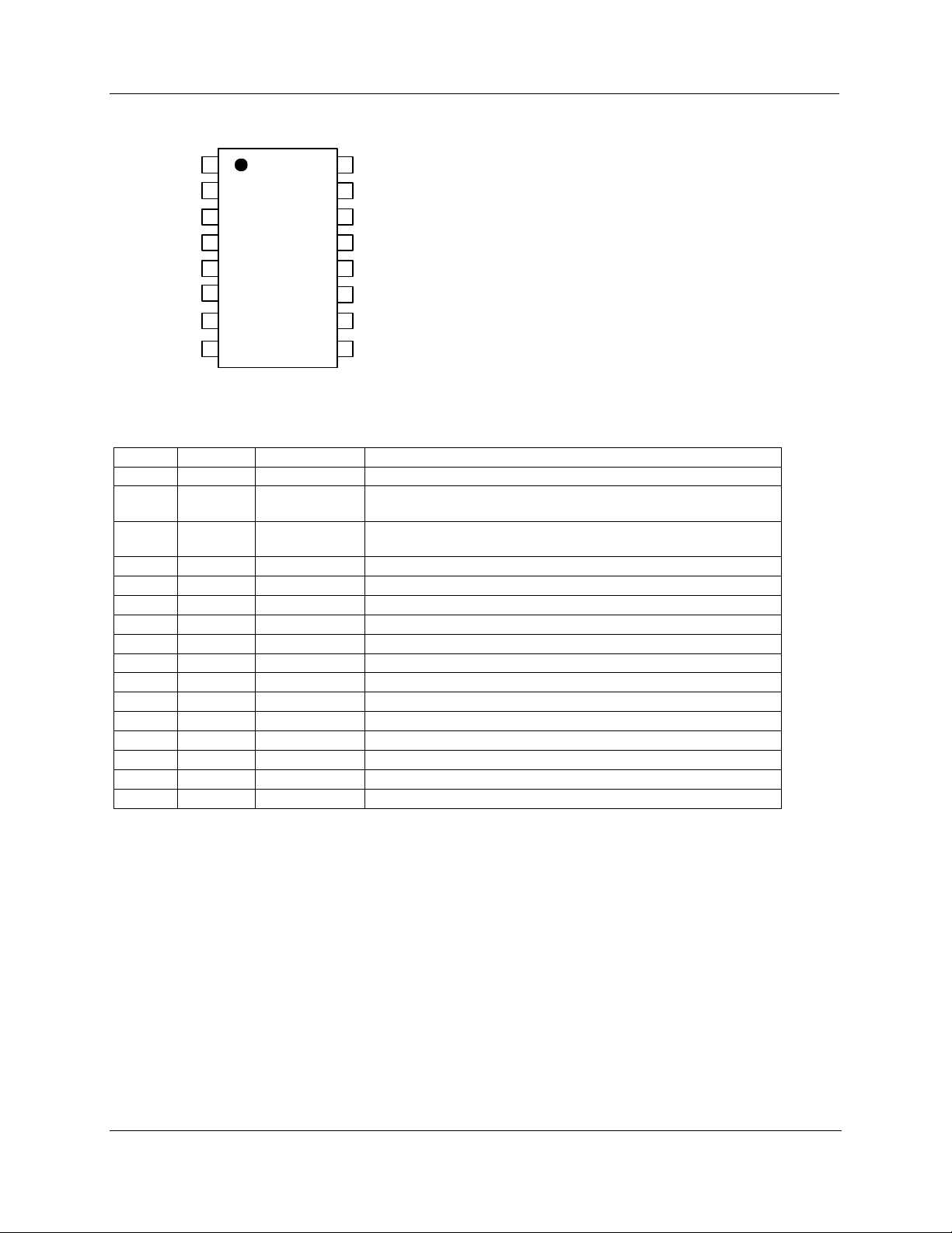
PIN CONFIGURATION
DVDD
NPD
NLDAC
DIN
SCLK
NCS
FS
1
2
3
4
5
6
7
8DGND 9 AGND
16
15
14
13
12
11
10
AVDD
REFINAB
OUTA
OUTB
OUTC
OUTD
REFINCD
PIN DESCRIPTION
PIN NO NAME TYPE DESCRIPTION
1
2
3
4
5
6
7
8
9
10
11
12
13
14
15
16
DVDD Supply Digital supply.
NPD Digital input Power down. Powers down all DACs overriding their individual power down
settings and all output stages. This pin is active low.
NLDAC Digital input Load DAC. Digital input active low. NLDAC must be taken low to update
the DAC latch from the holding latches.
DIN Digital input Serial data input.
SCLK Digital input Serial clock input.
NCS Digital input Chip select. This pin is active low.
FS Digital input Frame synchronisation for serial input data.
DGND Ground Digital ground.
AGND Ground Analogue ground.
REFINCD Analogue input Voltage reference input for DACs C and D.
OUTD Analogue output DAC D output.
OUTC Analogue output DAC C output.
OUTB Analogue output DAC B output.
OUTA Analogue output DAC A output.
REFINAB Analogue input Voltage reference input for DACs A and B.
AVDD Supply Analogue supply.
WOLFSON MICROELECTRONICS LTD PD Rev 1.0 June 1999
2
Page 3
WM2604 Production Data
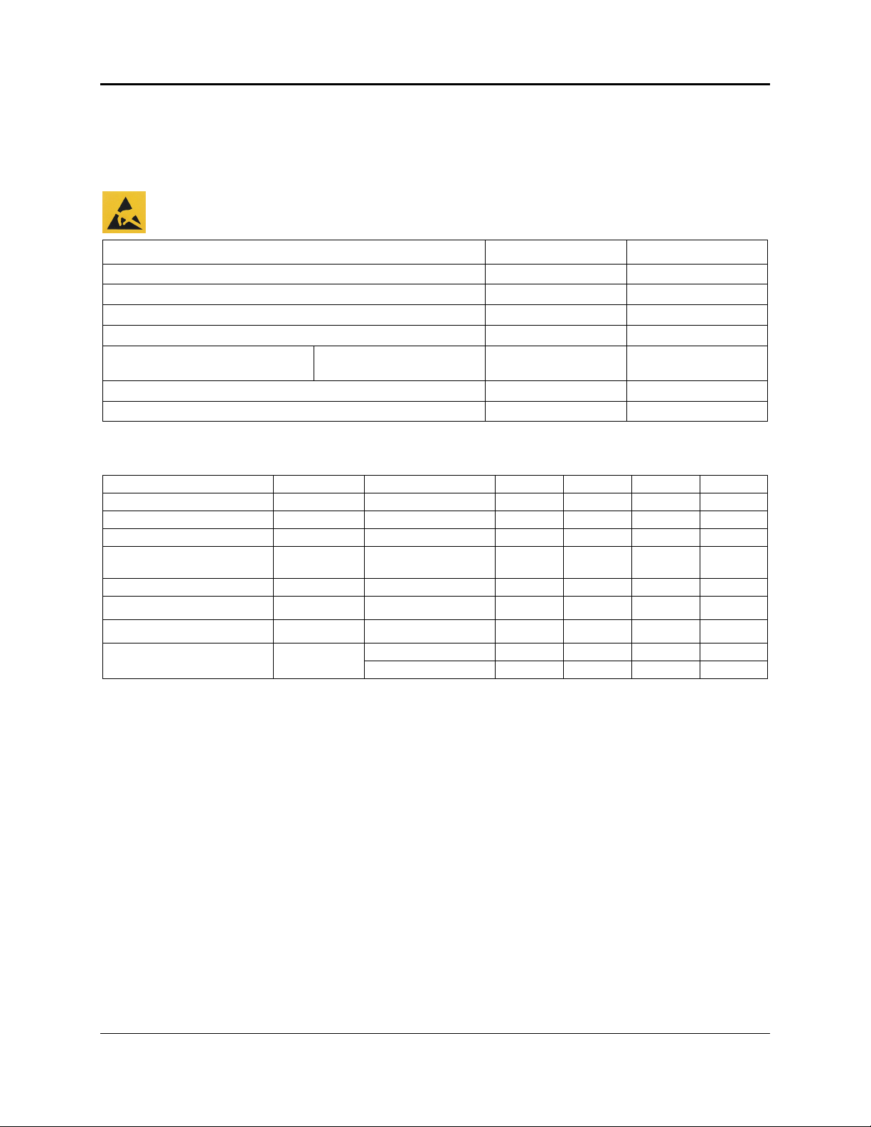
ABSOLUTE MAXIMUM RATINGS
Absolute Maximum Ratings are stress ratings only. Permanent damage to the device may be caused by continuously operating at or
beyond these limits. Device functional operating limits and guaranteed performance specifications are given under Electrical
Characteristics at the test conditions specified
ESD Sensitive Device. This device is manufactured on a CMOS process. It is therefore generically susceptible to
damage from excessive static voltages. Proper ESD precautions must be taken during handling and storage of this
device.
CONDITION MIN MAX
Supply voltages, AVDD to AGND, DVDD to DGND
Supply voltage differences, AVDD to DVDD
Digital input voltage
Reference input voltage
Operating temperature range, T
A
WM2604C
WM2604I
Storage temperature
Lead temperature 1.6mm (1/16 inch) soldering for 10 seconds
-2.8V 2.8V
-0.3V DVDD + 0.3V
-0.3V AVDD + 0.3V
0°C
-40°C
-65°C 150°C
7V
70°C
85°C
260°C
RECOMMENDED OPERATING CONDITIONS
PARAMETER SYMBOL TEST CONDITIONS MIN TYP MAX UNIT
Supply voltage
High-level digital input voltage
Low-level digital input voltage
Reference voltage to REFINAB,
REFINCD
Load resistance
Load capacitance
Serial clock rate
Operating free-air temperature
Note: Reference voltages greater than AVDD/2 will cause output saturation for large DAC codes.
AVDD, DVDD 2.7 5.5 V
V
f
V
V
REF
R
C
SCLK
T
IH
IL
L
L
A
DVDD = 2.7V to 5.5V 2 V
DVDD = 2.7V to 5.5V 0.8 V
See Note AVDD - 1.5 V
2 10 kΩ
100 pF
20 MHz
WM2604CDT 0 70 °C
WM2604IDT -40 85 °C
WOLFSON MICROELECTRONICS LTD PD Rev 1.0 June 99
3
Page 4
WM2604 Production Data
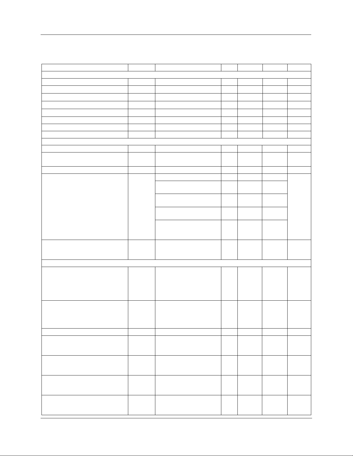
ELECTRICAL CHARACTERISTICS
Test Conditions:
RL = 10kΩ, CL = 100pF. AVDD = DVDD = 5V ±± 10%, V
recommended operating free-air temperature range (unless noted otherwise).
PARAMETER SYMBOL TEST CONDITIONS MIN TYP MAX UNIT
Static DAC Specifications
Resolution
Integral non-linearity
Differential non-linearity
Zero code error
Gain error
d.c. power supply rejection ratio
INL See Note 1
DNL See Note 2
ZCE See Note 3 3
GE See Note 4 0.25
DC PSRR See Note 5 0.5 mV/V
Zero code error temperature coefficient
Gain error temperature coefficient
DAC Output Specifications
Output voltage range
Output load regulation
Power Supplies
Active supply current
I
DD
Power down supply current
Dynamic DAC Specifications
Slew rate
Settling time
Glitch energy
Signal to noise ratio
Signal to noise and distortion ratio
Total harmonic distortion
Spurious free dynamic range
SNR fs = 400ksps, f
SNRD fs = 400ksps, f
THD fs = 400ksps, f
SPFDR fs = 400ksps, f
= 2.048V and AVDD = DVDD = 3V ±± 10%, V
REF
= 1.024V over
REF
10 bits
±±0.4 ±±1
±±0.1 ±±0.25
See Note 6 10 ppm/°C
See Note 6 10 ppm/°C
0 AVDD - 0.1 V
2kΩ to 10kΩ load
See Note 7
No load, V
= DVDD, V
IH
IL
= 0V
AVDD = 5V,
V
= 2.048V Slow
REF
AVDD = 5V,
V
= 2.048V Fast
REF
AVDD = 3V,
V
= 1.024V Slow
REF
AVDD = 3V,
V
= 1.024V Fast
REF
See Note 8
No load, all digital inputs
0V or DVDD
See Note 9
DAC code 32 to 1023,
10% to 90%
Slow
Fast
0.5
2.5
See Note 10
DAC code 32 to 1023
Slow
Fast
See Note 11
Code 511 to 512 10 nV-s
= 1kHz,
OUT
60 68 dB
BW = 20kHz
See Note 12
= 1kHz,
OUT
54 65 dB
BW = 20kHz
See Note 12
= 1kHz,
OUT
BW = 20kHz
See Note 12
= 1kHz,
OUT
54 70 dB
BW = 20kHz
See Note 12
0.1 0.25 %
1.4 2.2
3.5 5.5
1.0 1.5
3.0 4.5
0.01 10 µA
1.0
4.0
12.0
4.0
-68 -54 dB
±±12
±±0.6
LSB
LSB
mV
% FSR
mA
V/µs
V/µs
µs
µs
WOLFSON MICROELECTRONICS LTD PD Rev 1.0 June 1999
4
Page 5
WM2604 Production Data
Test Conditions:
RL = 10kΩ, CL = 100pF. AVDD = DVDD = 5V ±± 10%, V
recommended operating free-air temperature range (unless noted otherwise).
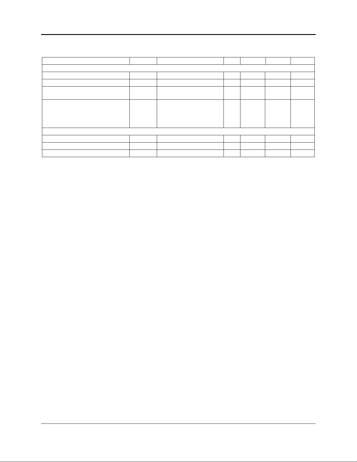
PARAMETER SYMBOL TEST CONDITIONS MIN TYP MAX UNIT
Reference
Reference input resistance
Reference input capacitance
R
C
REFIN
REFIN
Reference feedthrough
Reference input bandwidth
Digital Inputs
High level input current
Low level input current
Input capacitance
I
IH
I
IL
C
I
Notes:
1. Integral non-linearity (INL) is the maximum deviation of the output from the line between zero and full scale (excluding the effects of
zero code and full scale errors).
2. Differential non-linearity (DNL) is the difference between the measured and ideal 1LSB amplitude change of any adjacent two codes. A
guarantee of monotonicity means the output voltage changes in the same direction (or remains constant) as a change in digital input code.
3. Zero code error is the voltage output when the DAC input code is zero.
4. Gain error is the deviation from the ideal full scale output excluding the effects of zero code error.
5. Power supply rejection ratio is measured by varying AVDD from 4.5V to 5.5V and measuring the proportion of this signal imposed on
the zero code error and the gain error.
6. Zero code error and Gain error temperature coefficients are normalised to full scale voltage.
7. Output load regulation is the difference between the output voltage at full scale with a 10kΩ load and 2kΩ load. It is expressed as a
percentage of the full scale output voltage with a 10kΩ load.
8. IDD is measured while continuously writing code 512 to the DAC. For VIH < DVDD - 0.7V and VIL > 0.7V supply current will increase.
9. Typical supply current in power down mode is 10nA. Production test limits are wider for speed of test.
10. Slew rate results are for the lower value of the rising and falling edge slew rates.
11. Settling time is the time taken for the signal to settle to within 0.5LSB of the final measured value for both rising and falling edges. Limits
are ensured by design and characterisation, but are not production tested.
12. SNR, SNRD, THD and SPFDR are measured on a synthesised sinewave at frequency f
= 2.048V and AVDD = DVDD = 3V ±± 10%, V
REF
= 1.024V over
REF
10 MΩ
5 pF
V
= 1VPP at 1kHz
REF
-75 dB
+ 1.024V dc, DAC code 0
V
= 0.2VPP + 1.024V dc
REF
DAC code 512
Slow
Fast
0.5
1
Input voltage = DVDD 1 µA
Input voltage = 0V -1 µA
3 pF
generated with a sampling frequency fs
OUT
MHz
MHz
.
WOLFSON MICROELECTRONICS LTD PD Rev 1.0 June 99
5
Page 6
WM2604 Production Data
SERIAL INTERFACE
SCLK
DIN
t
WLtWH
1 2 3 4 5 15 16
t
SUDtHD
t
SUCSFS
D0D1D12D13D14D15
t
NCS
t
WHFS
t
SUFSCLK
t
SUC16FS
FS
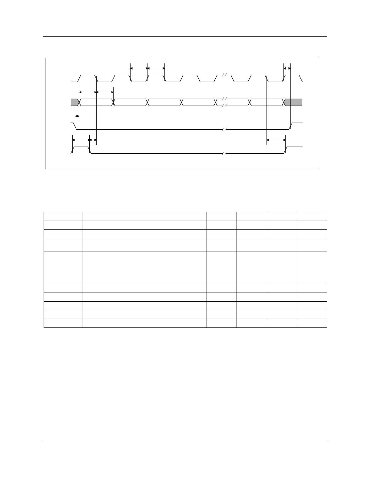
Figure 1 Timing Diagram
Test Conditions:
RL = 10kΩ, CL = 100pF. AVDD = DVDD = 5V ±± 10%, V
= 2.048V and AVDD = DVDD = 3V ±± 10%, V
REF
= 1.024V over
REF
recommended operating free-air temperature range (unless noted otherwise)
SYMBOL TEST CONDITIONS MIN TYP MAX UNIT
t
SUCSFS
t
SUFSCLK
t
SUC16FS
Setup time NCS low before negative FS edge.
Setup time FS low before first negative SCLK edge.
Setup time, sixteenth negative SCLK edge after FS low
on which D0 is sampled before rising edge of FS.
Setup time, sixteenth positive SCLK edge (first positive
10 ns
8 ns
10 ns
10 ns
after D0 sampled) before NCS rising edge.
t
SUC16CS
If FS is used instead of the sixteenth positive edge to
update the DAC, then the setup time is between the FS
rising edge and the NCS rising edge.
t
WHCLK
t
WLCLK
t
SUDCLK
t
HDCLK
t
WHFS
Pulse duration, SCLK high.
Pulse duration, SCLK low.
Setup time, data ready before SCLK falling edge.
Hold time, data held valid after SCLK falling edge.
Pulse duration, FS high.
25 ns
25 ns
8 ns
5 ns
20 ns
SUC16CS
WOLFSON MICROELECTRONICS LTD PD Rev 1.0 June 1999
6
Page 7
WM2604 Production Data
INL - LSB
OUTPUT VOLTAGE - V
OUTPUT VOLTAGE - V
OUTPUT VOLTAGE - V
OUTPUT VOLTAGE - V
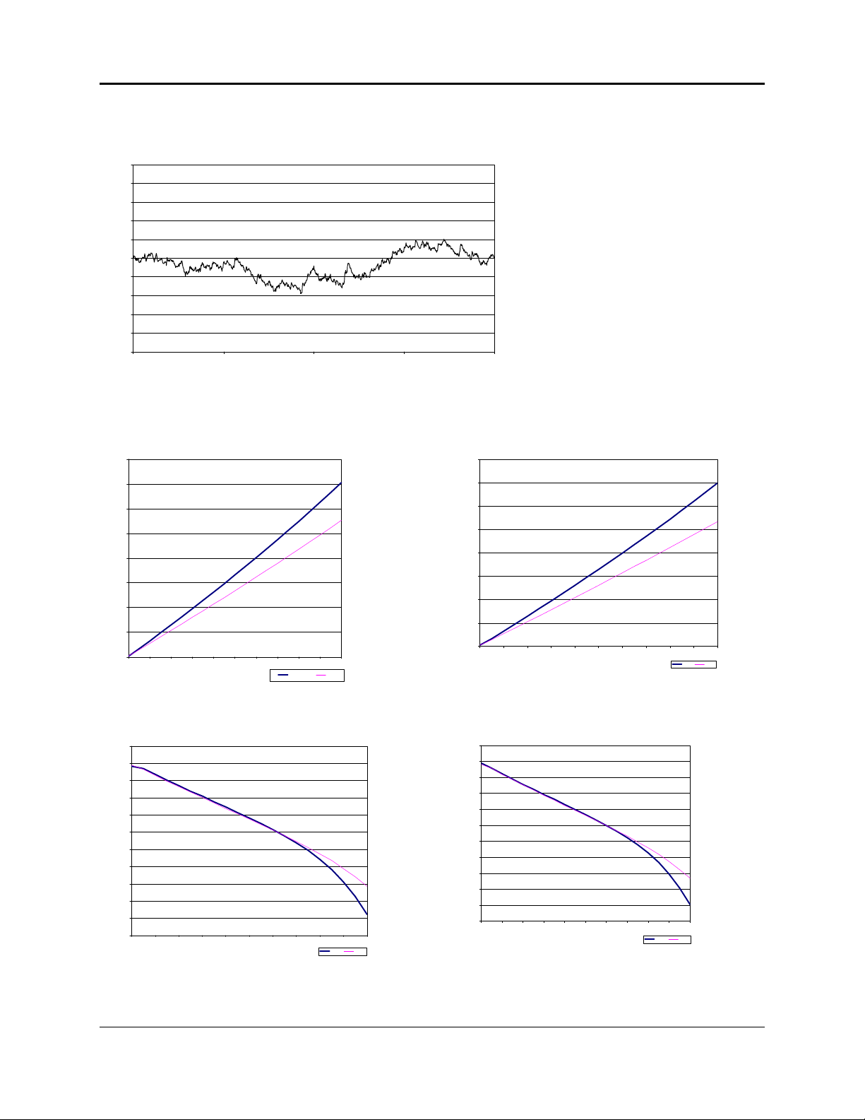
TYPICAL PERFORMANCE GRAPHS
1
AVDD = DVDD =5V, VREF =2.048V, Speed = Fast mode, Load = 10k/100pF
0.8
0.6
0.4
0.2
0
-0.2
-0.4
-0.6
-0.8
-1
0 256 512 767 1023
Figure 2 Integral Non-Linearity
0.4
AVDD = DVDD = 3V, V
0.35
0.3
0.25
0.2
0.15
0.1
0.05
0
0 1 2 3 4 5 6 7 8 9 10
= 1V, Input Code = 0
REF
ISINK - mA
DIGITAL CODE
Slow Fast
0.4
AVDD = DVDD = 5V, V
0.35
0.3
0.25
0.2
0.15
0.1
0.05
0
0 1 2 3 4 5 6 7 8 9 10
= 2V, Input Code = 0
REF
ISINK - mA
Slow Fast
Figure 3 Sink Current AVDD = DVDD = 3V Figure 4 Sink Current AVDD = DVDD = 5V
2.054
AVDD = DVDD = 3V, V
2.052
2.05
2.048
2.046
2.044
2.042
2.04
2.038
2.036
2.034
2.032
0 1 2 3 4 5 6 7 8 9 10
= 1V, Input Code = 1023
REF
ISOURCE - mA
Slow Fast
4.092
AVDD = DVDD = 5V, V
4.09
4.088
4.086
4.084
4.082
4.08
4.078
4.076
4.074
4.072
4.07
0 1 2 3 4 5 6 7 8 9 10
= 2V, Input Code = 1023
REF
ISOURCE - mA
Slow Fast
Figure 5 Source Current AVDD = DVDD = 3V Figure 6 Sink Current AVDD = DVDD = 5V
WOLFSON MICROELECTRONICS LTD PD Rev 1.0 June 99
7
Page 8
WM2604 Production Data
DEVICE DESCRIPTION
GENERAL FUNCTION
The device uses a resistor string network buffered with an op amp to convert 10-bit digital data to analogue
voltage levels (see Block Diagram). The output voltage is determined by the reference input voltage and
the input code according to the following relationship:
Output voltage =
INPUT OUTPUT
11 1111 1111
: :
10 0000 0001
10 0000 0000
01 1111 1111
: :
00 0000 0001
00 0000 0000 0V
Table 1 Binary Code Table (0V to 2V
CODE
( )
REF
V2
1024
( )
V2 REF
( )
V2 REF
512
( )
V2
1024
( )
V2 REF
( )
V2 REF
Output), Gain = 2
REFIN
1023
1024
513
1024
511
1024
1
1024
REFREF
=
V
POWER ON RESET
An internal power-on-reset circuit resets the DAC registers to all 0s on power-up.
BUFFER AMPLIFIER
The output buffer has a near rail-to-rail output with short circuit protection and can reliably drive a 2kΩ load
with a 100pF load capacitance.
EXTERNAL REFERENCE
The reference voltage input is buffered which makes the DAC input resistance independent of code.
REFINAB and REFINCD pins have an input resistance of 10MΩ and an input capacitance of typically
5pF. The reference voltage determines the DAC full-scale output.
HARDWARE CONFIGURATION OPTIONS
The device has two configuration options that are controlled by device pins.
DEVICE POWER DOWN
The device can be powered-down by pulling pin NPD (Pin 2) high. This powers down all DACs overriding
their individual power down settings. This will reduce power consumption to typically 10nA. When the
power down function is released the device reverts to the DAC code set prior to power down.
SIMULTANEOUS DAC UPDATE
The NLDAC pin (Pin 3) can be held high to prevent serial word writes from updating the DAC latches. By
writing new values to multiple DACs then pulling NLDAC low, all new DAC codes are loaded into the DAC
latches simultaneously.
WOLFSON MICROELECTRONICS LTD PD Rev 1.0 June 1999
8
Page 9
WM2604 Production Data
1
SERIAL INTERFACE
Explanation of data transfer:
First, the device has to be enabled with NCS set to low. Then, a falling edge of FS starts shifting the data
bit-per-bit (starting with the MSB) to the internal register on the falling edges of SCLK. After 16 bits have
been transferred, the next rising edge on SCLK or FS causes the content of the shift register to be moved
to the DAC holding latch. If NLDAC is low, the DAC latch will also be updated immediately.
The serial interface of the device can be used in two basic modes:
• four wire (with chip select)
• three wire (without chip select)
Using chip select (four wire mode), it is possible to have more than one device connected to the serial port
of the data source (DSP or microcontroller). If there is no need to have more than one device on the serial
bus, then NCS can be tied low.
SERIAL CLOCK AND UPDATE RATE
Figure 1 shows the device timing. The maximum serial rate is:
f
max = MHz20
SCLK
The digital update rate is limited to an 800ns period, or 1.25MHz frequency. However, the DAC settling
time to 10 bits limits the update rate for large input step transitions.
+
=
tt
minWCLminWCH
SOFTWARE CONFIGURATION OPTIONS
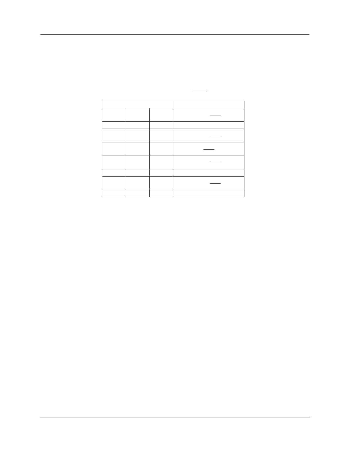
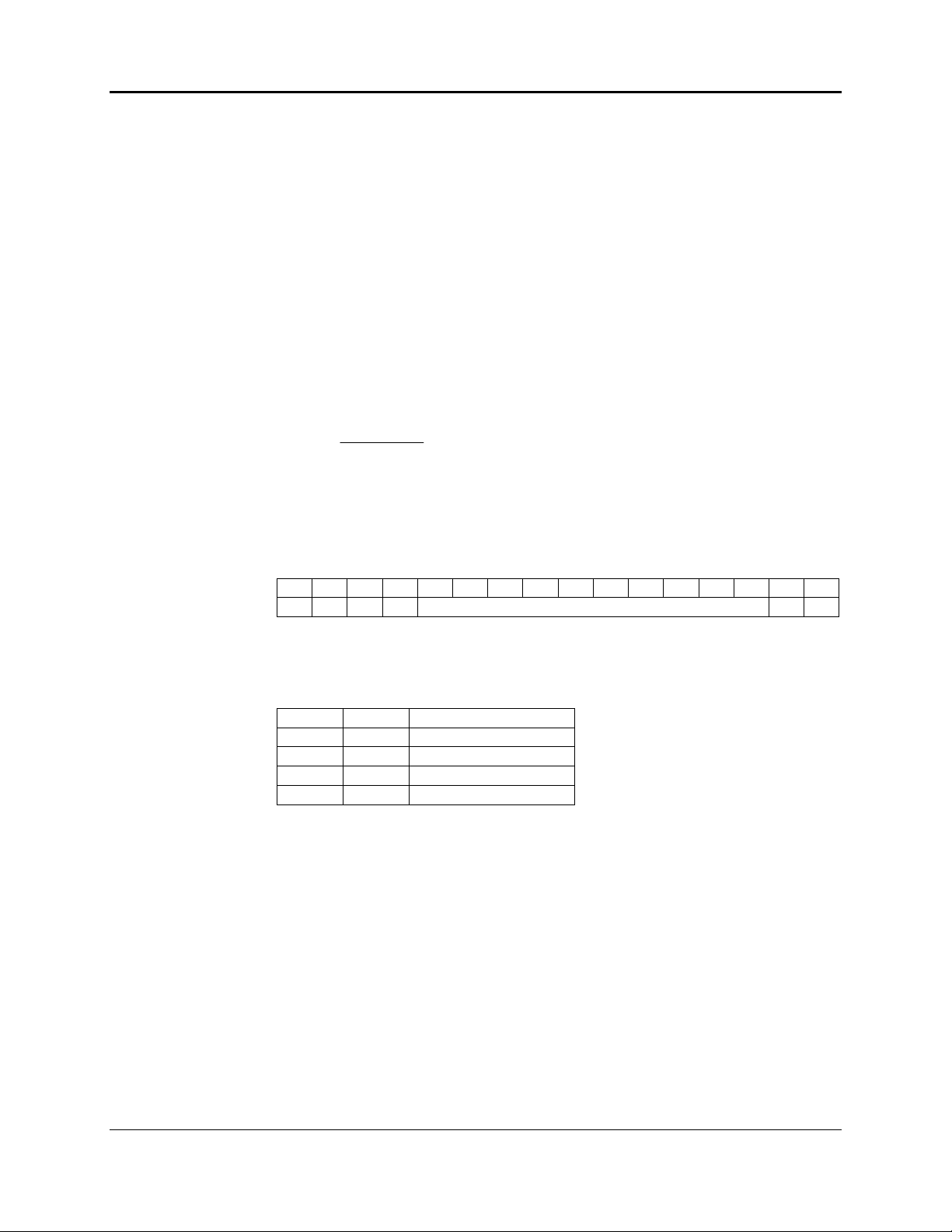
The 16 bits of data can be transferred with the sequence shown in Table 2. D11-D2 contains the
10-bit data word. D15-D12 hold the programmable options.
D15 D14 D13 D12 D11 D10 D9 D8 D7 D6 D5 D4 D3 D2 D1 D0
A1 A0 PWR SPD New DAC value (10 bits) X X
Table 2 Register Map
DAC ADDRESSING
A particular DAC (A, B, C, D) within the device is selected by A1 and A0 within the input word.
A1 A0 DAC ADDRESS
0 0 DAC A
0 1 DAC B
1 0 DAC C
1 1 DAC D
PROGRAMMABLE SETTLING TIME (SPD – BIT D12)
Settling time is a software selectable 12µs or 4µs, typical to within ±0.5LSB of final value. This is
controlled by the value of SPD – Bit D12 and an associated DAC address. A ONE defines a settling time
of 4µs, a ZERO defines a settling time of 12µs for that DAC.
PROGRAMMABLE POWER DOWN
The power down function is controlled by PWR - Bit D13 and an associated DAC address. A ZERO
configures that DAC as active, a ONE configures that DAC into power down mode.
WOLFSON MICROELECTRONICS LTD PD Rev 1.0 June 99
9
Page 10
WM2604 Production Data
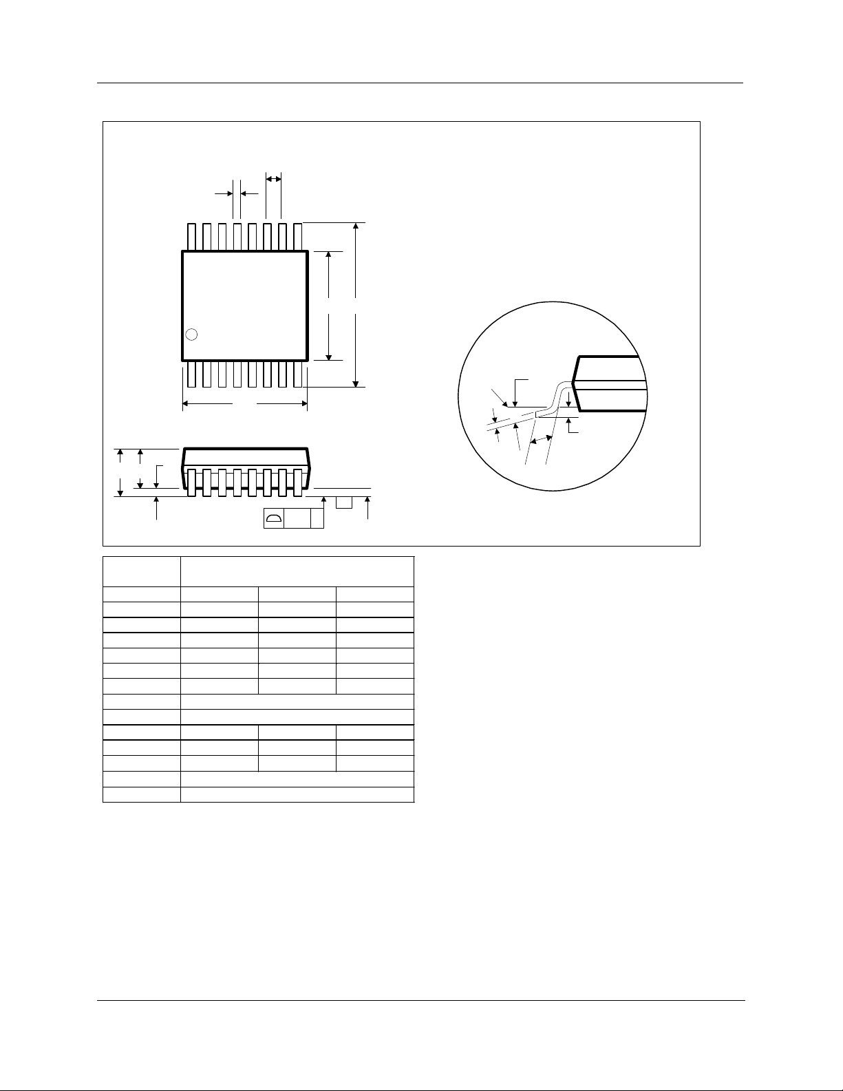
PACKAGE DIMENSIONS
DM013.ADT: 16 PIN TSSOP (5.0 x 4.4 x 1.0 mm)
b
A2
A1
A
e
916
D
81
0.05
Dimensions
Symbols
(mm)
MIN NOM MAX
A
A
1
A
2
b
c
D
----- ----- 1.20
0.05 ----- 0.15
0.80 1.00 1.05
0.19 ----- 0.30
0.09 ----- 0.20
4.90 5.00 5.10
e 0.65 BSC
E
E
1
L
θθ
4.30 4.40 4.50
0.45 0.60 0.75
o
0
6.4 BSC
----- 8
E1 E
C
-C-
SEATING PLANE
o
GAUGE
PLANE
θθ
0.25
c
L
REF:
NOTES:
A. ALL LINEAR DIMENSIONS ARE IN MILLIMETERS.
B. THIS DRAWING IS SUBJECT TO CHANGE WITHOUT NOTICE.
C. BODY DIMENSIONS DO NOT INCLUDE MOLD FLASH OR PROTRUSION, NOT TO EXCEED 0.25MM.
D. MEETS JEDEC.95 MO-153, VARIATION = AB. REFER TO THIS SPECIFICATION FOR FURTHER DETAILS.
WOLFSON MICROELECTRONICS LTD PD Rev 1.0 June 1999
JEDEC.95, MO-153
10
 Loading...