

Page 1
WM0834, WM0838
2. Not available on WM0834
W
4
D
8-Bit ADCs with Serial Interface and
Configurable Input Multiplexer
Production Data
Sept 1996 Rev 2.0
Description
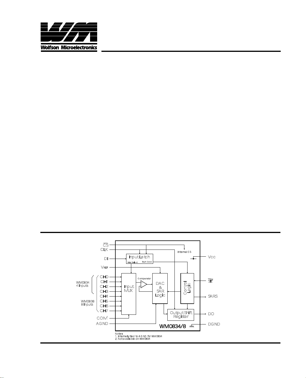
WM0834 and WM0838 are 8-bit analogue to digital
converters (ADC) with configurable 4-input and 8-input
multiplexers respectively and a serial I/O interface.
Assignment of the multiplexer inputs is configured before
each conversion via the serial data input to give single-ended
or differential operation for the selected inputs. A mixture of
input configurations can be used in the same application.
WM0838 also has a pseudo-differential configuration where
all 8 inputs can be refered to a common input at an arbitrary
voltage.
Serial communcation with WM0834/8 is via Data In (DI) and
Data Out (DO) wires under the control of clock and chip
select inputs. A high output at the SARS pin indicates when
the conversion is in progress. T o initiate a conversion chip
enable is held low and data is input to DI on the rising edge
of the clock, comprising, a start bit, and bits to set up the
input configuration and polarity . After a half clock cycle delay
conversion results appear at DO on the falling edge of the
clock, MSB first, concurrently with A-D conversion. This is
followed by the results LSB first, indicated by the falling edge
of SARS. WM0838 has a shift enable (SE) input used to
control the LSB first output on DO.
WM0834/8 operate on 5V and 3.3V supply voltages and
are available in small outline and DIP packages for commercial (0 to 70
O
C) and industrial (-40 to 85OC) tempera-
ture ranges.
Block Diagram
CS
CLK
DI
V
REF
Input Latch
Start Conv
Mux Select
Features
• Functionally Equivalent to National Semiconductor ADC0834 and ADC0838 without the Internal
Zener Regulator Network
• 4-input (WM0834) or 8-input (WM0838) MUX
options
• Reference input operates ratiometrically or with
a fixed reference
• Input range 0 to Vcc with Vcc Reference
• 5V and 3.3V variants
• Total Unadjusted Error: ± 1 LSB
• 8-bit resolution
• Low Power
µµ
• 32
µs conversion time at fclock
µµ
• Serial I/O interface
= 250 kHz
• WM0834 packages: 14 pin SO & DIP
WM0838 packages: 20 pin wide-body SO & DIP
Applications
• Embedding with remote sensors
• Equipment health monitoring
• Automotive
• Industrial control
Internal CS
Vcc
CH0
M0834
Inputs
WM0838
8 Inputs
Production Data data sheets contain final
specifications current on publication date. Supply
of products conforms to Wolfson Microelectronics
standard terms and conditions.
CH1
CH2
CH3
CH4
CH5
CH6
CH7
1
COM
AGND
Notes:
1. Internally tied to AGND for WM0834
Wolfson Microelectronics
Lutton Court, Bernard Terrace, Edinburgh EH8 9NX, UK
Tel: +44 (0) 131 667 9386 Fax: +44 (0) 131 667 5176
Input
MUX
Comparator
DAC
&
SAR
Logic
Output Shift
Register
WM0834/8
email: [email protected]
www: http://www.wolfson.co.uk
Logic
Control
2
SE
SARS
DO
DGN
© 1996 Wolfson Microelectronics
Page 2
WM0834, WM0838
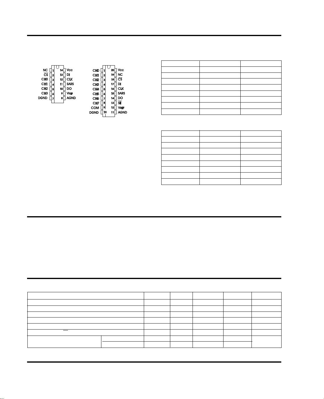
Top View
WM0834 : N(DIP) and D (SO) packages
WM0838: N(DIP) and DW (SO) packages
WM0834
Ordering InformationPin Configuration
5V devices
DEVICE TEMP. RANGE PACKAGE
WM0834CN 0
WM0834CD 0oC to 70oC 14 pin plastic SO
WM0834IN -40oC to 85oC 14 pin plastic DIP
WM0834ID -40oC to 85oC 14 pin plastic SO
WM0838CN 0oC to 70oC 20 pin plastic DIP
WM0838CDW 0oC to 70oC 20 pin plastic SO
WM0838IN -40oC to 85oC 20 pin plastic DIP
WM0838IDW -40oC to 85oC 20 pin plastic SO
o
C to 70oC 14 pin plastic DIP
WM0838
3.3V devices
DEVICE TEMP . RANGE PACKAGE
WM0834LCN 0oC to 70oC 14 pin plastic DIP
WM0834LCD 0oC to 70oC 14 pin plastic SO
WM0834LIN -40oC to 85oC 14 pin plastic DIP
WM0834LID -40oC to 85oC 14 pin plastic SO
WM0838LCN 0oC to 70oC 20 pin plastic DIP
WM0838LCDW 0oC to 70oC 20 pin plastic SO
WM0838LIN -40oC to 85oC 20 pin plastic DIP
WM0838LIDW -40oC to 85oC 20 pin plastic SO
Absolute Maximum Ratings (note 1)
Supply Voltage, Vcc (note 2) . . . . . . . . . . . 6.5 V
Input voltage range:
Digital Inputs . . . . GND - 0.3 V, VCC + 0.3 V
Analogue inputs . . . GND - 0.3 V, VCC + 0.3 V
Input current, any pin (note 3) . . . . . . ± 5 mA
Total Input current for package . . . . . . ± 20 mA
Operating temperature range, TA . . . . TMIN to TMAX
WM083_C_ (C suffix) . . . . . . . . . 0
WM083_I_ (I suffix) . . . . . . . . . . -40
Storage Temperature . . . . . . . . - 65
Soldering Information:
Lead Temperature 1.6 mm (1/16) from case
for 10 seconds: D, DW or N package . . . . . . . 260
o
C to +70oC
o
C to +85oC
o
C to +150oC
o
C
Recommended Operating Conditions (5V)
SYMBOL MIN NOMINAL MAX UNIT
Supply voltage VCC 4.5 5 5.5 V
High level input voltage VIH 2V
Low level input voltage VIL 0.8 V
Clock frequency fclock 10 600 KH z
Clock duty cycle (see Note 4) Dclk 40 60 %
Pulse duration CS high t wH(CS) 220 ns
Operating free-air temperature C suffix TA 070
I Suffix T A -40 85
o
C
2
Wolfson Microelectronics
Page 3
WM0834, WM0838
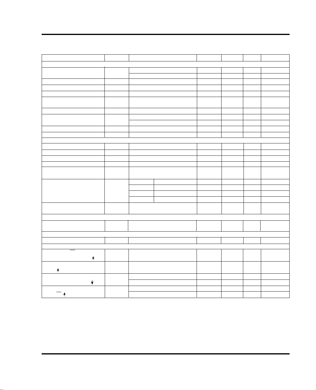
Electrical Characteristics (5V)
VCC = 5.0V , VREF = 5V , fCLK = 250 KHz, TA = TMIN to TMAX , tr = tf = 20ns, unless otherwise stated.
PARAMETER SYMBOL TEST CONDITIONS MIN TYP MAX UNIT
Digital Inputs
High level output voltage V
Low level output voltage VOL VCC = 5.25 V, IOH = 1.6 mA 0.4 V
High level input current IIH VIH = 5 V 0.005 1 µA
Low level input current IIL VIL = 0 V -0.005 -1 µA
High level output (source) IOH VOH = 0 V -6.5 -24 mA
current
Low level output (sink) current IOL VOL = VCC 826 mA
High impedance-state I OZ VO = 5 V 0.01 3 µA
output current (DO) VO = 0 V -0.01 -3 µA
Input capacitance Ci 5pF
Output capacitance Co 5pF
Converter and Multiplexer
T otal unadjusted error TUE VREF = 5 V. (note 7) ±1 LSB
Differential Linearity (note 8) 8 Bits
Supply voltage variation error Vs(error) VCC = 4.75 V to 5.25 V ±1/16 ±1/4 LSB
Common mode error Differential mode ±1/16 ±1/4 LSB
Common mode input voltage VICR (note 9) GND-0.05 V
range VCC+0.05
Standby input leakage II(stdby) On-channel VI = 5 V at ON ch. 1 µA
current (note 10) Off-channel VI = 0 V at OFF ch. -1 µA
Conversion time tconv Excluding MUX addressing time 8 clock
Reference Inputs
Input resistance to Ri(REF) 1.3 2.4 5.9 kΩ
reference ladder
Total device
Supply current ICC 0.6 1.25 mA
Timing Parameters
Setup time, CS low or tsu 350 ns
data valid before clock
Hold time, data valid after th 90 ns
clock
Propagation delay time, MSB data first. CL = 100 pF 1500 ns
output data after clock
Output disable time, DO tdis CL = 10 pF, RL = 10 kΩ 125 250 ns
after CS
OH VCC = 4.75 V , I OH = -360 mA 2.4 V
VCC = 4.75 V, IOH = -10 mA 4.5 V
On-channel VI = 0 V at ON ch. -1 µA
Off-channel VI = 5 V at OFF ch. 1 µA
periods
tpd LSB data first. CL = 100 pF 600 ns
CL = 100 pF, RL = 2 kΩ 500 ns
Wolfson Microelectronics
3
Page 4
WM0834, WM0838
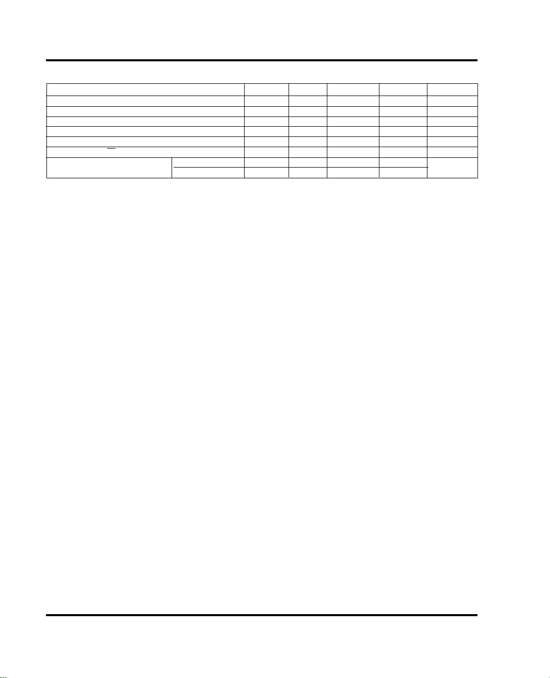
Recommended Operating Conditions (3.3V)
SYMBOL MIN NOMINAL MAX UNIT
Supply voltage VCC 2.7 3.3 3.6 V
High level input voltage VIH 2V
Low level input voltage VIL 0.8 V
Clock frequency (Vcc = 3.3V) fclock 10 600 KHz
Clock duty cycle (see Note 4) Dclk 40 60 %
Pulse duration CS high t wH(CS) 220 ns
Operating free-air temperature C suffix TA 070
I Suffix T A -40 85
o
C
4
Wolfson Microelectronics
Page 5
WM0834, WM0838
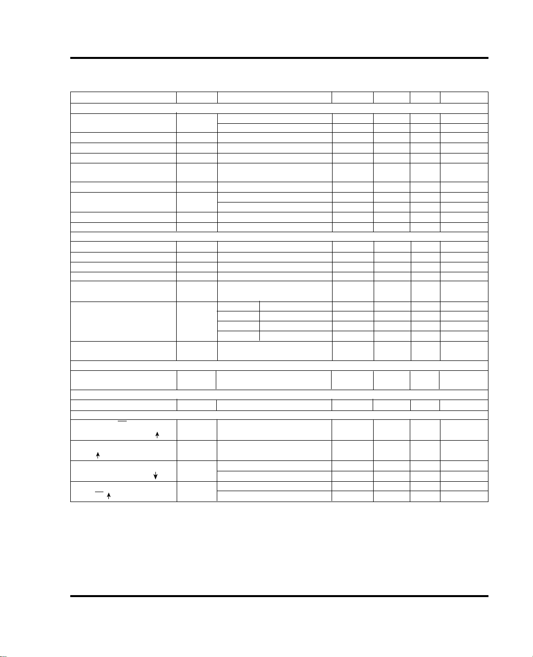
Electrical Characteristics (3.3V)
VCC = 3.3V, fCLK = 250 KHz, TA = TMIN to TMAX , tr = tf = 20ns, unless otherwise stated.
PARAMETER SYMBOL TEST CONDITIONS MIN TYP MAX UNIT
Digital Inputs
High level output voltage V
Low level output voltage VOL VCC =3.0V, IOH = 1.6 mA 0.4 V
High level input current IIH VIH = 3.6V 0.005 1 µA
Low level input current IIL VIL = 0 V -0.005 -1 µA
High level output (source) IOH VOH = 0 V , TA = 25oC6.515 mA
current
Low level output (sink) current IOL VOL = VCC, TA = 25oC8 16 mA
High impedance-state I OZ VO = 3.3 V, T A = 25oC 0.01 3 µA
output current (DO) VO = 0 V , TA = 25oC -0.01 -3 µA
Input capacitance Ci 5pF
Output capacitance Co 5pF
Converter and Multiplexer
T otal unadjusted error TUE VREF = 3.3 V. (note 7) ±1 LSB
Differential Linearity (note 8) 8 Bits
Supply voltage variation error Vs(error) VCC = 3.0 V to 3.6 V ±1/16 ±1/4 LSB
Common mode error Differential mode ±1/16 ±1/4 LSB
Common mode input voltage VICR (note 9) GND-0.05 V
range VCC+0.05
Standby input leakage II(stdby) On-channel VI =3.3 V at ON ch. 1 µA
current (note 10) Off-channel VI = 0 V at OFF ch. -1 µA
Conversion time tconv Excluding MUX addressing time 8 clock
Reference Inputs
Input resistance to Ri(REF) 1.3 2.4 5.9 kΩ
reference ladder
Total device
Supply current ICC 0.2 0.75 mA
Timing Parameters
Setup time, CS low or tsu 350 ns
data valid before clock
Hold time, data valid after th 90 ns
clock
Propagation delay time, MSB data first. CL = 100 pF 500 ns
output data after clock
Output disable time, DO tdis CL = 10 pF, RL = 10 kΩ 80 ns
after CS
OH VCC = 3.0 V , I OH = -360 mA 2.4 V
VCC = 3.0V, IOH = -10 mA 2.8 V
On-channel VI = 0 V at ON ch. -1 µA
Off-channel VI =3.3V at OFF ch 1 µA
periods
tpd LSB data first. CL = 100 pF 200 ns
CL = 100 pF, RL = 2 kΩ 250 ns
Wolfson Microelectronics
5
Page 6

WM0834, WM0838
Electrical Characteristics (continued)
Notes:
1. Absolute Maximum Ratings are stress ratings only.
Permanent damage to the device may be caused by
continuously operating at or beyond these limits. Device functional operating range limits are given under
Recommended Operating Conditions. Guaranteed
performance specifications are given under Electrical
Characteristics at the test conditions specified.
6. All parameters are measured under open-loop
conditions with zero common mode input voltage
(unless otherwise stated).
7. T otal Unadjusted Error (TUE) is the sum of integral linearity error, zero code error and full scale error over
the output code range.
2. All voltage values, except differential voltages are with
respect to the ground.
3. When the input voltage V
power supply rails (GND > V
of current at that pin should be limited to 5 mA or less.
at any pin exceeds the
IN
> VCC) the absolute value
IN
The 20 mA package input current limits the number of
pins that can exceed the power supply boundaries
with a 5 mA supply current to four.
4. A clock duty cycle range of 40% to 60% ensures
correct operation at all clock frequencies. For a clock
with a duty cycle outside these limits, the minimum time
the clock is high or low must be at least 666 ns, with
the maximum time for clock high or low being 60 ms.
5. All typical values are at V
devices and V
CC = 3.3 V, T
CC = 5 V, T
= 25oC for 3.3V devices.
A
= 25oC for 5V
A
8. A Differential linearity of "n" bits ensures a code width
exist to "n" bits. Hence a Differential Linearity of 8 bits
for an 8 bit ADC guarantees no missing codes.
9. For V
(-) greater than or equal to VIN(+) the digital out-
IN
put code will be 00 Hex. Connected to each analogue
input are two diodes which will forward conduct for a
diode drop outside the supply rails, V
analogue input voltage does not exceed the supply volt-
and GND. If an
CC
age by more than 50 mV, the output code will be correct. T o use an absolute input voltage range of 0 to V
a minimum VCC - 0.05 V is required for all variations of
temperature. Care should be exercised when testing at
levels with a maximum analogue voltage as
low V
CC
this can cause the input diode to conduct, especially at
high temperature, and cause errors for analogue inputs
near full scale.
10. Standby input leakage currents, are currents going in
or out of the on or off channels when the ADC is not
performing conversion and the clock input is in a high
or low steady-state condition.
CC
6
Wolfson Microelectronics
Page 7
Test Circuits and Waveforms
V
GND
C
C
D
(
V
D
D
D
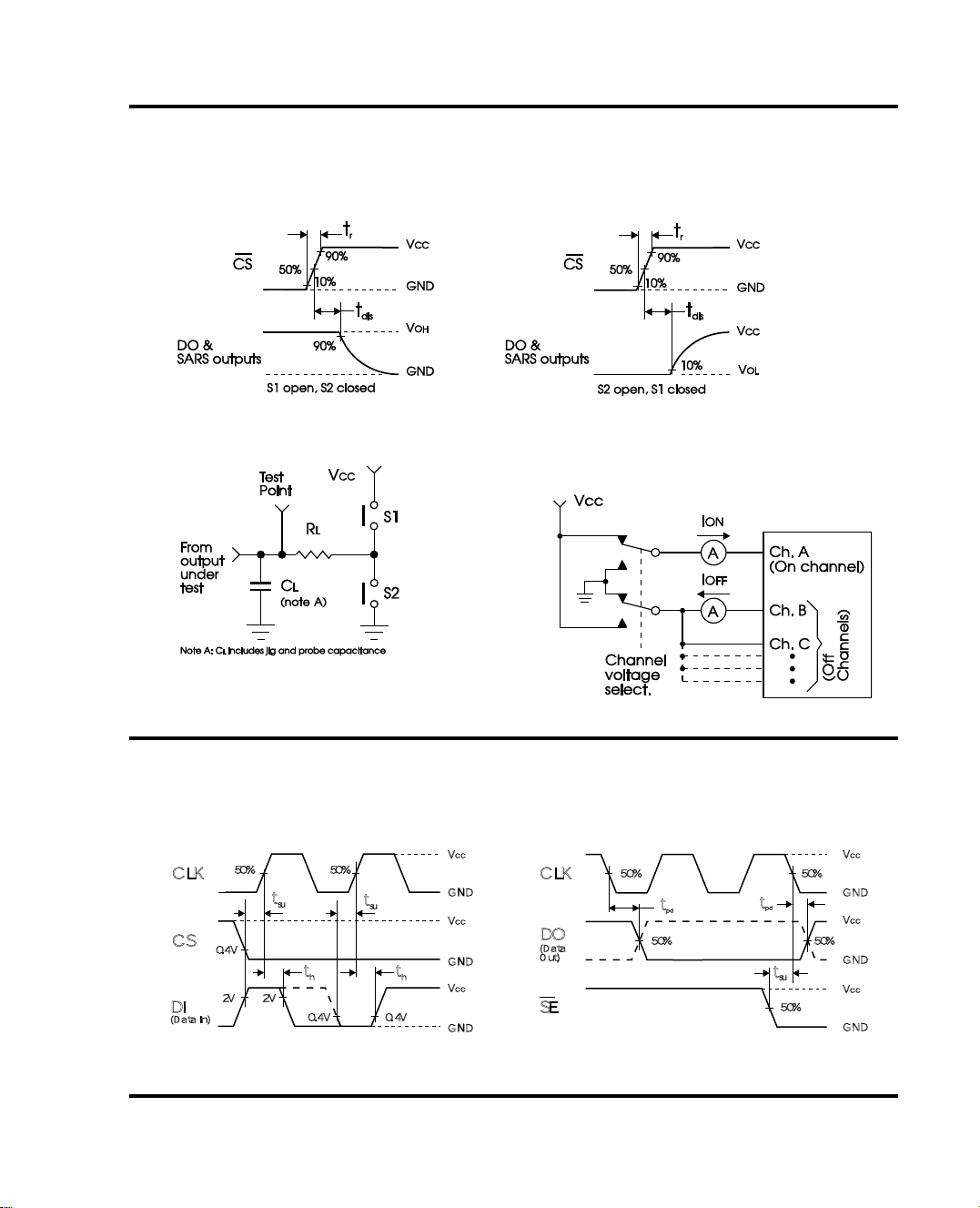
Output Disable Time Voltage Waveforms and Test Circuits
WM0834, WM0838
Standby Leakage Current Test Circuit
Detailed Timing Diagrams
Data Input Timing
50% 50%
LK CLK
S
I
Data In)
0.4V
2V 2V
t
su
t
0.4V 0.4V
t
su
h
t
cc
GND
V
cc
GND
h
V
cc
DO
(Data
Out)
SE
Wolfson Microelectronics
Data Output Timing
50%
t
pd
50%
cc
50%
50%
GN
V
GN
V
GN
cc
cc
t
pd
t
su
50%
7
Page 8
WM0834, WM0838
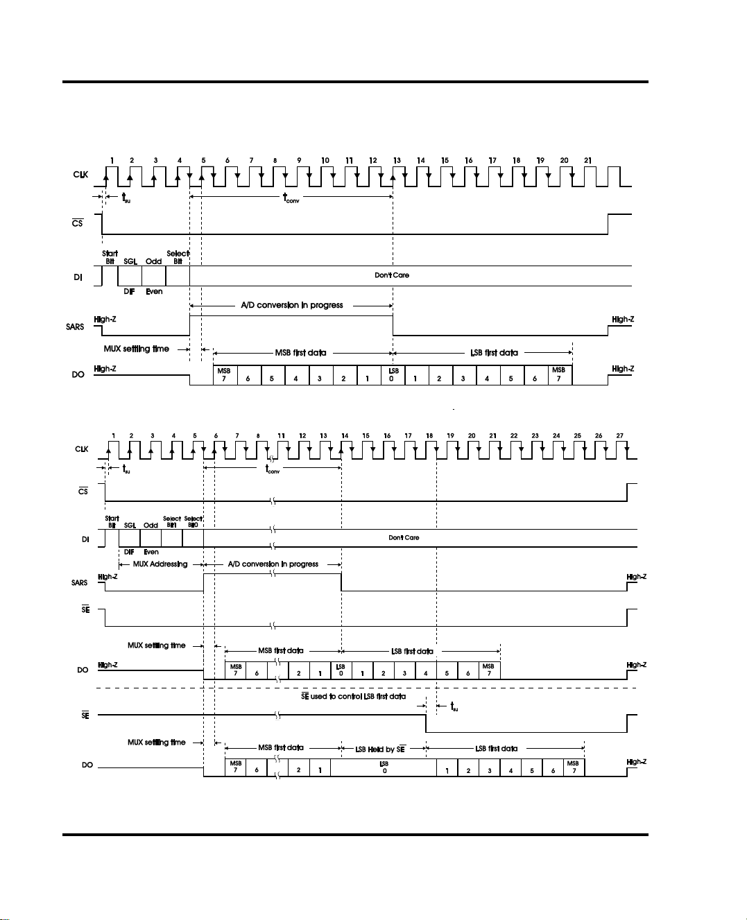
Functional Timing Diagrams
WM0834 Timing
WM0838 Timing
8
Wolfson Microelectronics
Page 9
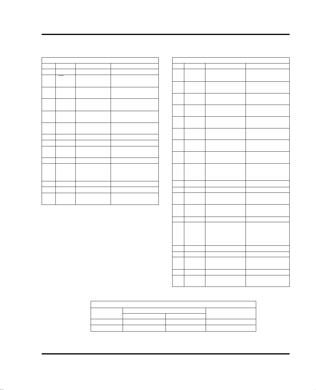
Pin Descriptions
WM0834, WM0838
WM0834
Pin Name Type Function
1 NC No connection
2 CS Digital Chip Select
(active low)
3 CH0 Analogue input Channel 0 input
to multiplexer (MUX)
4 CH1 Analogue input Channel 1 input
to multiplexer (MUX)
5 CH2 Analogue input Channel 2 input
to multiplexer (MUX)
6 CH3 Analogue input Channel 3 input
to multiplexer (MUX)
7 DGND Supply Digital ground pin
8 AGND Supply Analogue ground pin
9VREF Analogue input Voltage reference
input
10 DO Digital output Data output
11 SARS Digital output Successive
approximation
registar status line
12 CLK Digital input Clock input
13 DI Digital input Data input
14 VCC Supply Positive supply
voltage
WM0832
Pin Name Type Function
1 CH0 Analogue input Channel 0 input
to multiplexer (MUX)
2 CH1 Analogue input Channel 1 input to
multiplexer (MUX)
3 CH2 Analogue input Channel 2 input to
multiplexer (MUX)
4 CH3 Analogue input Channel 3 input to
multiplexer (MUX)
5 CH4 Analogue input Channel 4 input to
multiplexer (MUX)
6 CH5 Analogue input Channel 5 input to
multiplexer (MUX)
7 CH6 Analogue input Channel 6 input to
multiplexer (MUX)
8 CH7 Analogue input Channel 7 input to
multiplexer (MUX)
9 COM Analogue input Common input for
pseudo differential
mode
10 DGND Supply Digital ground pin
11 AGND Supply
12 VREF Analogue input Voltage reference
13 SE Digital input Shift enable control
14 DO Digital output Data Output
15 SARS Digital output Successive
16 CLK Digital input Clock input
17 DI Digital input Data input
18 CS Digital Chip Select
19 NC No connection
20 VCC Supply Positive supply
Analogue ground pin
input
line (active low)
approximation
register status line
output
(active low)
voltage
Multiplexer / Package Options
Device Number of Analogue Channels Number of
No Single Ended Differential Package Pins
WM0834 4 2 14
WM0838 8 4 20
Wolfson Microelectronics
9
Page 10

WM0834, WM0838
Functional Description
Multiplexer Operation and Addressing
WM0834 and WM0838 use an input multiplexer scheme
thet provides multiple analogue channels, configurable for
single-ended or differential operation and also for WM0838,
a pseudo-differential mode that will perform an analogue to
digital (A/D) conversion of the voltage difference between
any analogue input and a common terminal (COM).
The start bit and the MUX assignment bits on DI are
clocked in on the rising edges of the clock input, which
may be generated by the processor or run continuously.
WM0834 uses three MUX assignment bits and WM0838
uses four.
WM0834/8 uses a successive approximation routine to
perform A/D conversion that employs a sample data
comparator structure which always performs conversion on
a differential voltage. Conversion takes place on the
voltage difference between assigned "+" and "-" inputs and
the converter expects the "+" input to be the most positive. If
the "+" input is more negative than "-" then the converter
gives an all zeros output.
Assignment of inputs is made for a single-ended signal
between an "+" input and analogue ground (AGND) or COM
for WM0838, or for differential inputs between adjacent pairs
of inputs of either polarity.
The COM input of WM0838 acts as the "-" input for pseudodifferential "+" inputs and can be an arbitrary voltage such
as an analogue common not at ground potential in single
supply applications.
Prior to the start of every conversion the input configuration
is assigned during the MUX addressing sequence achieved
by serially shifting data into the Data Input (DI) on the rising
edges of the clock input.
The MUX address selects which analogue inputs are
enabled, either single-ended, differential or pseudodifferential (WM0838). For differential inputs the polarity of
the selected pairs of adjacent inputs are also assigned.
Differential inputs can only be assigned to adjacent channel
pairs.
When the logic "1" start bit is clocked into the start
conversion location of the multiplexer input register, the
analogue MUX inputs are selected. After 1/2 a clock
period delay to allow for the selected MUX output to
settle, the conversion commences using the successive
approximation technique. At this time, the SARS output
goes high to indicate a conversion is in progress and the
DI input is disabled.
When conversion begins, the A/D conversion result from
the output of the SARS comparator appears at the DO
output on each falling edge of the clock (see Functional
Timing Diagrams).
With the successive approximation A/D conversion
routine, the analogue input is compared with the output of
a digital to analogue converter (DAC) for each bit by the
SARS comparator and a decision made on whether the
analogue input is higher or lower than the DAC output.
Successive bits, MSB to LSB are input to the DAC and
remain in its input if the analogue comparison decides the
analogue input is higher than the DAC output. If not, the
bit is removed from the DAC input. The output from the
SARS comparator forms the resulting input to the DAC
and the A/D conversion output, and is read by the
processor as conversion takes place in MSB to LSB
order. After 8 clock periods, the conversion is complete
and this is indicated by SARS being brought low a 1/2
clock period later.
The MUX addressing tables give full details of input
assignments.
Initiating Conversion and the Digital Interface
WM0834 and WM0838 are controlled from a processor via
a serial interface comprising Data In (DI) and Data Out (DO),
Chip Select (CS) and Clock (CLK) inputs and a SAR
Status (SARS) output.
A conversion is initiated by pulling the chip select (CS) line
low. CS must be kept low for an entire conversion.
Wolfson Microelectronics
10
All bits of the conversion are stored in an output shift
register after a conversion has completed and MSB first
data has been output.
For WM0838, the commencement of output data in a LSB
first format can be controlled by use of the SE input. If
the SE input is held high, the LSB output will remain on
the DO output. When SE is brought low, LSB first data
output will begin on DO. After 8-bits of LSB first data have
been output, the DO output goes low and remains low
until CS is brought high, when outputs (DO & SARS) go
into a high impedance state.
Page 11
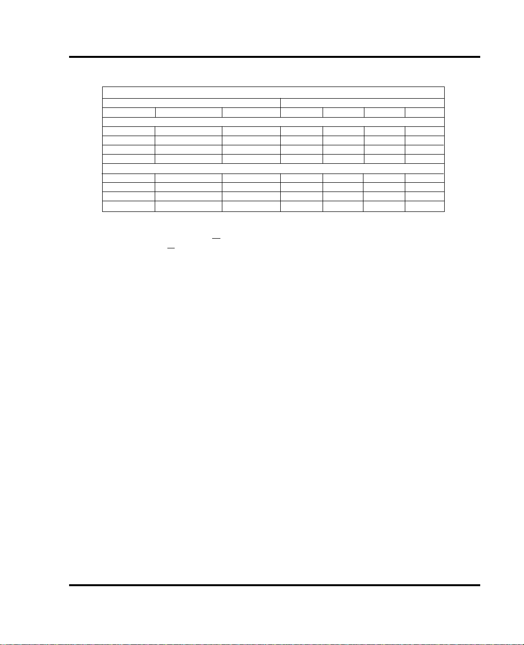
Functional Description (continued)
WM0834 MUX Addressing
MUX Address Channel Number
SGL/DIF ODD/EVEN Select bit 0 1 2 3
Differential MUX Mode (Between adjacent pairs of points)
00 0+ 00 1 +01 0-+
01 1 -+
Single Ended MUX Mode (between selected input(s) and AGND)
10 0+
10 1 +
11 0 +
11 1 +
Note: Analogue common input 'COM' used with single ended mode is internally tied to AGND
WM0834, WM0838
All internal registers are cleared when CS is high. To
initiate another conversion, CS must make a high to low
transition and MUX address assignments input to DI.
The DI inpit and DO output can be tied together and
controlled via a bidirectional processor I/O bit line.
Reference Input
The analogue input voltage range Vmax to Vmin for
differential and pseudo-differential input is defined by the
voltage applied to the reference input with respect to
AGND.
WM0834/8 can be used in ratiometric appliacations or
those requiring absolute accuracy. A ratiometric input is
typically the Vcc and is the same supply used to power
analogue input circuitry and sensors. In such systems
under a given input condition, the same code will be
output with variations in supply voltage, because the same
ratio change occurs in both the analogue and reference
input to the A/D. When used in applications requiring absolute accuracy, a suitable time and temperature stable
voltage reference source should be used.
The voltage source used to drive the reference input should
be capable of driving the 2.4kΩ typical of the SAR resistor
ladder. The maximum input voltage to the reference input
is the Vcc supply voltage. The minimum can be as least
as low as 1V to allow for direct conversion of sensor
outputs with output voltage ranges less than 5V.
Analogue Inputs
While sampling the analogue inputs, short spikes of
current enter a "+" input and flow out of the corresponding
"-" input at the clock edges during conversion. This
current does not cause errors as it decays rapidly and the
internal comparator is strobed at the end of a clock period.
Care should be exercised if bypass capacitors are used at
the inputs as an apparant offset error can be caused by the
capacitor averaging the input current and developing a voltage across the source resistance. Bypass capacitors should
not be used with a source resistance greater than 1kΩ.
In considering error sources, input leakage current will also
cause a voltage drop across the source resistance and
hence, high impedance sources should be buffered.
In differential mode, there is a 1/2 clock period interval
between sampling the "+" and the "-" inputs. If there is a
change in common mode voltage during this interval, an
errorcould notionally result.
For a sinusoidal common mode signal, the error is given
by:
VERROR = VPEAK (2πfCM) (1/(2fCLK))
Where V
PEAK = peak common mode voltage
CM = common mode signal frequency
f
fCLK = clock frequency
Wolfson Microelectronics
11
Page 12
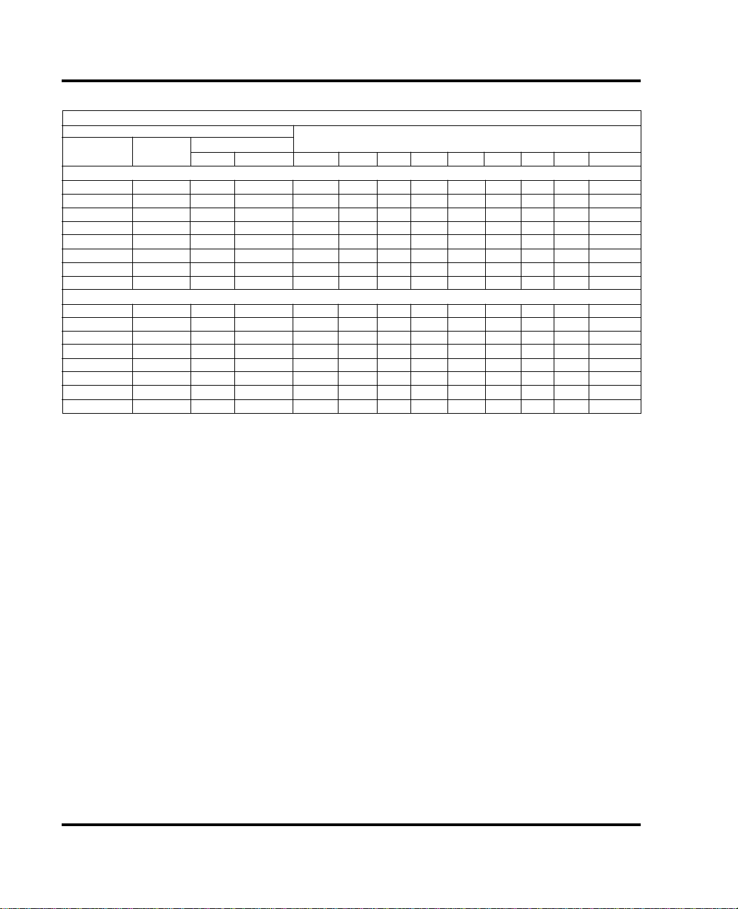
WM0834, WM0838
WM0838 MUX Addressing
MUX Address
SGL/ ODD/ Select biits Channel Number
DIF EVEN 1 0 0 1 2 3 4 5 6 7 COM
Differential MUX Mode (between adjacent pairs of inputs)
0000+0001 +0010 +0011 +0100-+
0101 -+
0110 -+
0111 -+
Single Ended MUX Mode (between selected input(s) and 'COM' pseudo analogue ground)
1000+ 1001 + 1010 + 1011 + 1100 + 1101 + 1110 + 1111 +-
12
Wolfson Microelectronics
Page 13
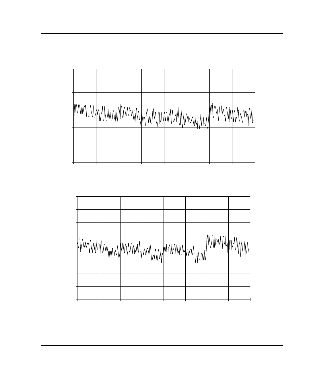
Performance Data
1
0.75
0.5
0.25
0
-0.25
Error (lsbs)
-0.5
-0.75
-1
0 32 64 96 128 160 192 224 256
WM0834, WM0838
WM0834: Total Unadjusted Error
Code
1
0.75
0.5
0.25
0
Error (lsbs)
-0.25
-0.5
-0.75
-1
0 32 64 96 128 160 192 224 256
Code
WM0838: Total Unadjusted Error
T est conditions: VDD = 5V , VREF = 5V , Temp = 25oC, FCLK = 250kHz
Wolfson Microelectronics
13
Page 14
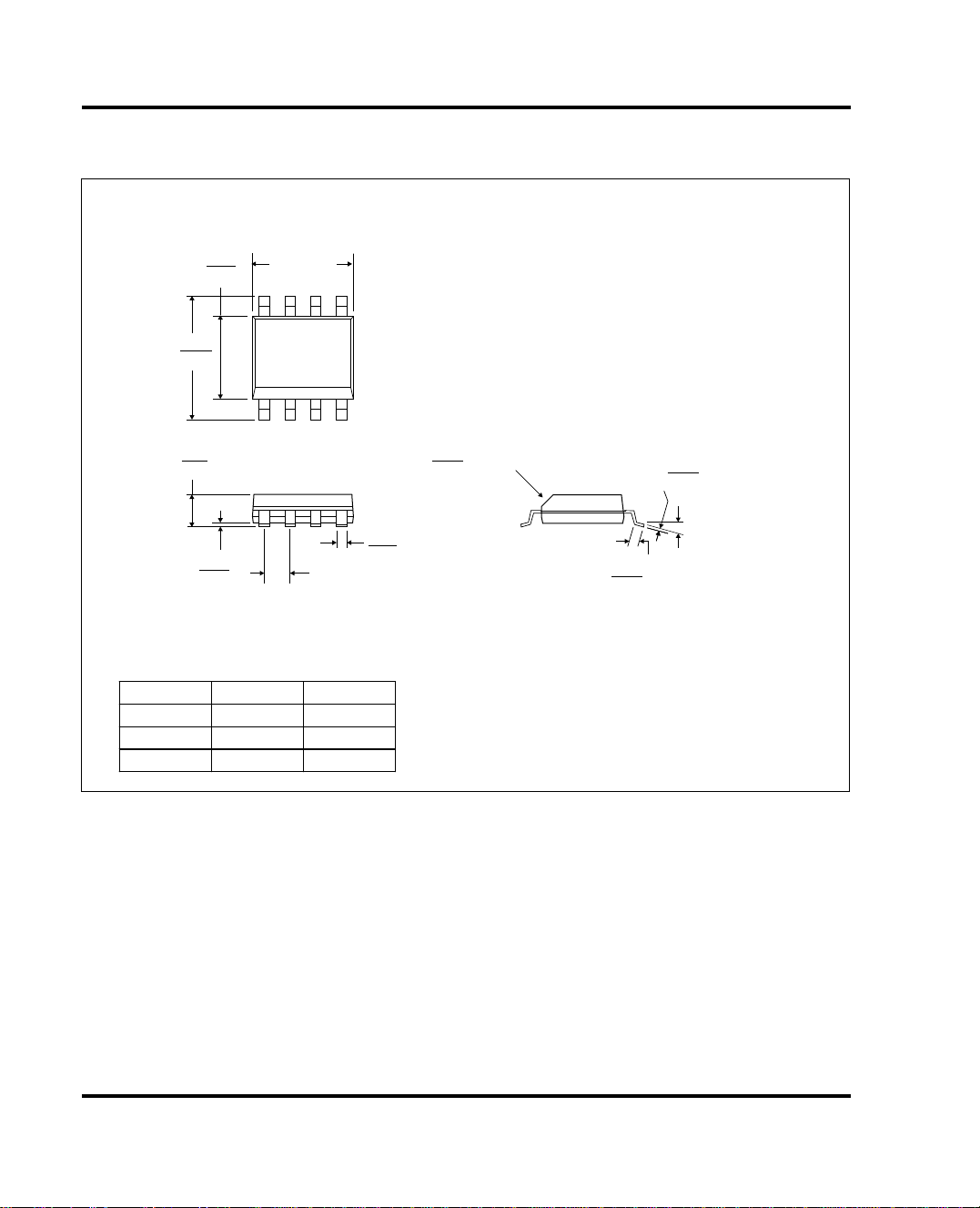
WM0834, WM0838
Package Descriptions
Plastic Small-Outline Package
D - 8 pins shown
4.00
3.80
6.20
5.80
1.75
1.35
0.25
0.10
A
14
Pin spacing
1.27 B.S.C.
Dimension 'A' Variations
NMinMax
8 4.80 5.00
14 8.55 8.75
16 9.80 10. 00
58
0.50
O
0.51
0.33
0.25
x 45 NOM
1.27
0.40
0.25
0.19
OO
0 to 8
Notes:
A. Dimensions in millimeters.
B. Complies with Jedec standard MS-012.
C. This drawing is subject to change without notice.
D. Body dimensions do not include mold flash or protrusion.
E. Dimension A, mould flash or protrusion shall not exceed 0.15mm. Body width, interlead flash or protrusions shall
not exceed 0.25mm.
Rev. 1 November 96
Wolfson Microelectronics
14
Page 15
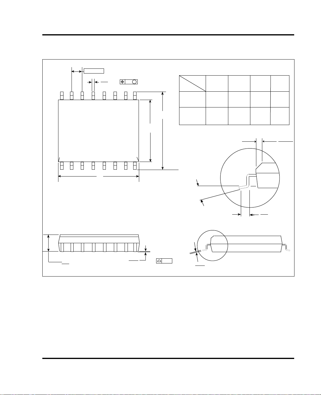
Package Description
Wide body Plastic Small-Outline Package
1,27 B.S.C.
0,51
16
0,33
0,25 M
WM0834, WM0838
DW - 16 pin shown
PINS**
9
DIM
A MAX
16
10,50
20
13,00
24
15,60
28
18,10
10,65
10,00
7,60
7,40
18
2,65
2,35
A
0,30
0,10
0,10
A MIN
0,33
0,23
0o - 8
10,10
o
12,60
Gauge Plane
15,20
1,27
0,40
17,70
0.75 x 45
0.25 x 45
Notes:
A. Dimensions in millimeters.
B. Complies with Jedec standard MS-013.
C. This drawing is subject to change without notice.
D. Body dimensions do not include mold flash or protrusion.
E. Dimension A, mould flash or protrusion shall not exceed 0.15mm. Body width, interlead flash or protrusions shall not
exceed 0.25mm.
0
0
Wolfson Microelectronics
Rev. 1 November 96
15
Page 16
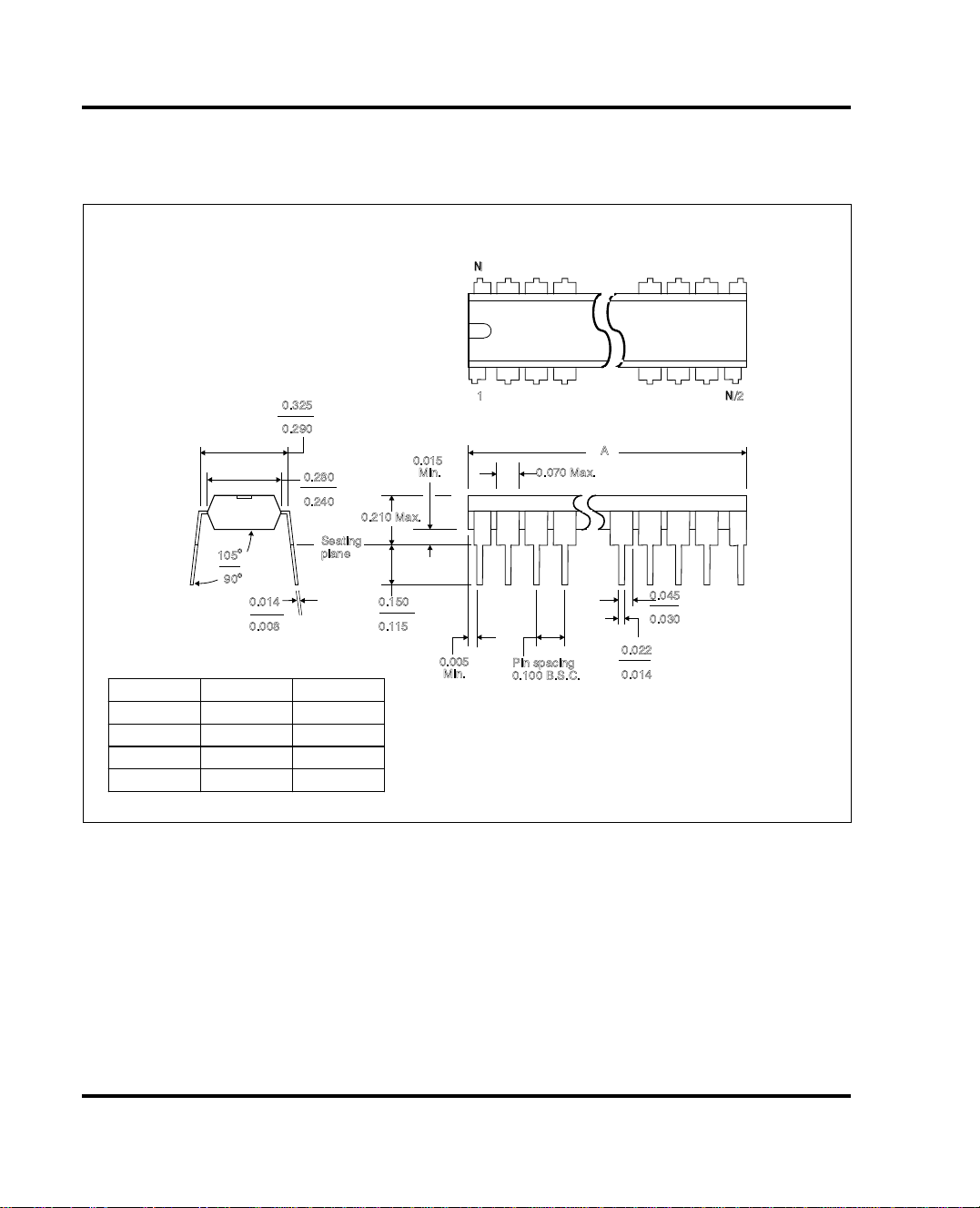
WM0834, WM0838
Package Descriptions
Dual-In-Line Package
N or P
N
0.005
Min.
1
0.070 Max.
Pin spacing
0.100 B.S.C.
A
0.045
0.030
0.022
0.014
O
105
O
90
0.014
0.008
Dimension 'A' Variations
0.325
0.290
0.280
0.240
Seating
plane
0.210 Max.
0.150
0.115
0.015
Min.
NMinMax
8 0.355 0.400
14 0.735 0.775
16 0.735 0.775
20 0.940 0.975
Notes:
A. Dimensions are in inches
B. Falls within JEDEC MS-001( 20 pin package is shorter than MS-001)
C. N is the maximum number of terminals
D. All end pins are partial width pins as shown, except the 14 pin package which is full width.
N/2
16
Rev. 1 November 96
Wolfson Microelectronics
 Loading...