

Page 1
The WL600C is a 2.4-2.5GHz RF transmitter and
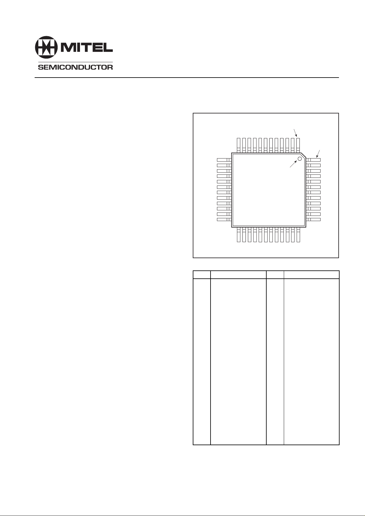
PIN 48
PIN 1 IDENT
PIN 1
receiver chip for use in digital radio, and operates from a
supply voltage of 2.7 - 3.6V. It is designed to work with the
Mitel Semiconductor WL800 frequency synthesiser and
the WL102 WLAN controller chip which together make up
the DE6038 frequency hopping Wireless Local Area
Network (WLAN) transceiver.
The receiver circuit contains a low noise amplifier,
image rejecting mixer, IF limiting strip with RSSI and a
quadrature demodulator. There is also a power amplifier
driver stage and ramp control facility for use in transmit.
FEATURES
■ Part of DE6038 chipset (WL800, WL102)
■ High level of integration
■ Low noise figure
■ Low power consumption
■ High data rates with comparator for 2 level FSK
■ Minimal external components
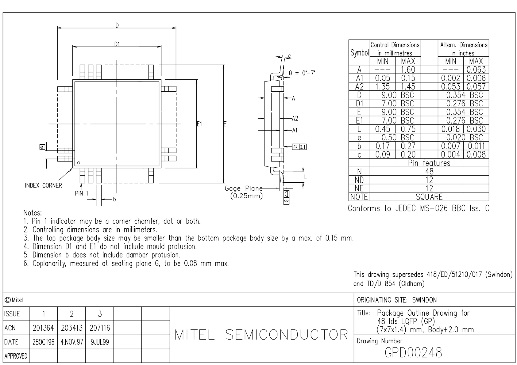
■ 48 lead LQFP package
WL600C
2.4 - 2.5GHz RF and IF Circuit
Preliminary Information
DS4581 2.1 August 1997
LQFP48
Fig.1 Pin connections - top view
ABSOLUTE MAXIMUM RATINGS
Supply voltage Vcc 4V
Transmit/Receive and standby input -0.5 to Vcc +0.5V
Current consumption TBD
Junction temperature Tj 150°
ESD protection 2KV
ORDERING INFORMATION
WL600C/KG/GP1R
RELATED DOCUMENTS
Datasheets WL800/102 DE6038
Pin Description Pin Description
1 QUAD+ 25 VCC_RF
2 QUAD- 26 GND_RF
3 GND_IF 27 VCC_LNA
4 DEMOD_OUT+ 28 GND_RF
5 DEMOD_OUT- 29 RF_IN
6 RSSI 30 LNA_DEGEN
7 CLAMP_SET 31 LNA_DEGEN
8 CCA_THRESHOLD 32 DRIVE
9 VCC_IFSTRIP 33 VCC_PA
10 DECOUPLE_LOG- 34 GND_RF
11 DECOUPLE_LOG+ 35 RAMP_CAP
12 IF_IN+ 36 PA_ON
13 IF_IN- 37 STDBYB
14 CCAB 38 TX/RXB
15 GND_IF 39 GND_LO
16 BUFFER_IN+ 40 LO_IN
17 BUFFER_IN- 41 VCC_LO
18 VCC_DATA 42 DATA_IN+
19 RXD 43 DATA_IN20 RXDB 44 BUFFER_OUT21 GND_RF 45 BUFFER_OUT+
22 IF_OUT- 46 CLAMP23 IF_OUT+ 47 CLAMP+
24 GND_PADDLE 48 GND_PADDLE
Page 2
WL600C
29
LNA
32
35
IMAGE
REJECT
MIXER
IMAGE
REJECT
MIXER
PA DRIVE
BUFFER
LO
BUFFER
40 12
PHASE
SHIFT
PHASE
SHIFT
PHASE
SHIFT
13
22 23 46 47 7
ACTIVE
CLAMP
CIRCUIT
IF STRIP
DETECTORS
6
42
BUFFER
AMP
COMPARATOR
43
DATA
SLICE
19
20
16
44
X2
45
17
10
11
1
2
4
5
14
8
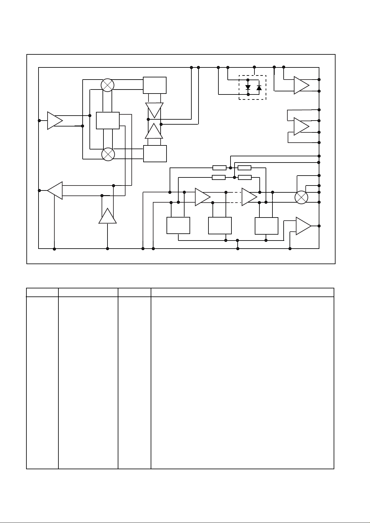
Fig. 2 WL600C block diagram
DEVICE PIN OUT
Pin Ref Type Description
1 QUAD+ I/O Quadrature demodulator tank circuit connection
2 QUAD - I/O Quadrature demodulator tank circuit connection
3 GND_IF GND Ground for IF strip circuitry
4 DEMOD_OUT + OUT Demodulator output
5 DEMOD_OUT - OUT Demodulator output
6 RSSI OUT RSSI detector analogue output
7 CLAMP_SET IN Sets clamp knee voltage
8 CCA_THRESHOLD IN Sets level at which CCA comparator will switch
9 VCC_IFSTRIP VCC Power supply for log amp, demod, and internal references
10 DECOUPLE_LOG - I/O Decoupling for log amp feedback network, AC couple
11 DECOUPLE_LOG + I/O Decoupling for log amp feedback network, AC couple
12 IF_IN + IN Log amp input, AC couple
13 IF_IN - IN Log amp input, AC couple
14 CCAB OUT CCA comparator output: signal = logic high, clear = logic low
15 GND_IF GND Ground for IF strip circuitry
16 BUFFER_IN + IN x 2 buffer input
17 BUFFER_IN - IN x 2 buffer input
18 VCC_DATA VCC Power supply for clamp, data comparator and buffer amp
19 RXD OUT Data comparator output
2
Page 3

WL600C
Pin Ref Type Description
20 RXDB OUT Data comparator output
21 GND_RF GND Ground for LNA, mixer, IF summation, and PA driver circuits
22 IF_OUT- OUT Downconverter output, requires external load and RFC
23 IF_OUT+ OUT Downconverter output, requires external load and RFC
24 GND_PADDLE GND Ground for substrate and package paddle
25 VCC_RF VCC Power supply for mixer, summation, and PA ramp circuits
26 GND_RF GND Ground for LNA, mixer, IF summation, and PA driver circuits
27 VCC_LNA VCC Power supply for LNA
28 GND_RF GND Ground for LNA, mixer, IF summation, and PA driver circuits
29 RF_IN IN LNA input, AC couple
30 LNA_DEGEN I/O LNA degeneration, connect to ground
31 LNA_DEGEN I/O LNA degeneration, connect to ground
32 DRIVE OUT Power amplifier driver output, requires external load and RFC
33 VCC_PA VCC Power supply for power amplifier driver
34 GND_RF GND Ground for LNA, mixer, IF summation, and PA driver circuits
35 RAMP_CAP I/O PA ramp circuit timing capacitor connection
36 PA_ON IN PA ramp circuit control input:
PA on = logic high, PA off = logic low
37 STDBYB IN Power down control input:
active= logic high, standby = logic low
38 TX/RXB IN Transmit/Receive control input:
transmit = logic high, receive = logic low
39 GND_LO GND Ground for LO buffer, phaseshifter, and standby circuitry
40 LO_IN IN Local oscillator input, AC couple
41 VCC_LO VCC Power supply for LO buffer, phaseshifter, and standby circuitry
42 DATA_IN+ IN Data comparator input
43 DATA_IN- IN Data comparator input
44 BUFFER_OUT- OUT x2 buffer output
45 BUFFER_OUT+ OUT x2 buffer output
46 CLAMP - I/O Data clamp, knee voltage set by pin 7, AC couple
47 CLAMP + I/O Data clamp, knee voltage set by pin 7, AC couple
48 GND_PADDLE GND Ground for substrate and package paddle
3
Page 4
WL600C
ELECTRICAL CHARACTERISTICS
These characteristics are guaranteed over the following conditions (unless otherwise stated):
T
= -20°C to + 85°C VCC = 2.7V to 3.6V,
AMB
Characteristic Value Unit Condition
Min Typ Max
Supply current (transmit) 50 mA
Supply current (Receive) 60 mA
Supply current in standby 0.3 mA
PA DRIVER & RAMP CIRCUIT
Logic low voltage 0 0.8 V Ramp down
Logic high voltage Vcc-0.7 Vcc V Ramp up
Logic Input current 10 µA
Ramp capacitor charge Current 250 µA
Ramp capacitor voltage swing 1 V
Output power -2 2 dBm
Output band 2.4 2.5 GHz
Max to Min power out ratio 20 dB
RECEIVER LOW NOISE
AMPLIFIER & MIXERS
Conversion gain 19 22 dB Differential into 600Ohms
3rd order intercept point -10 dBm
1dB input gain compression -22 dBm
Noise figure 7 10 dB Matched to 50Ohms
Input impedance 2.4GHz 13+j20 Ohms
2.45GHz 15+j30
2.5GHz 20+j50
Image frequency rejection 25 dB
Local oscillator input level -16 dBm
Local oscillator input impedance 15-j40 Ohms
IF output impedance 600 Ohms With external 900Ω resistor
TRANSMIT/RECEIVE INPUT
Logic low voltage 0 0.8 V Receive mode
Logic high voltage Vcc-0.7 Vcc V Transmit mode
Input current 10 µA
4
Page 5

ELECTRICAL CHARACTERISTICS (cont)
These characteristics are guaranteed over the following conditions (unless otherwise stated):
T
= -20°C to + 85°C VCC = 2.7V to 3.6V,
AMB
Characteristic Value Unit Condition
Min Typ Max
LIMITING STRIP
Maximum input frequency 50 MHz
Noise figure 3.5 6 dB
Input resistance 1200 Ohms Set by external 1k8 resistor
Capacitance 0.5 pF
Limiting strip gain 70 dB
Limiting point -78 -75 dBm
RSSI
Rise time 100 ns
Non linearity ±3dB
Maximum output voltage 1.9 V Input = 0dBm
Output voltage @ -70dBm input 1.3 V
Output impedance 6 kOhms
CLEAR CHANNEL
ASSESSMENT COMPARATOR
Logic high voltage 2.2 V
Logic low voltage 0.5 V
Threshold input limits 1 2 V
Input current 1 µA
DEMODULATOR
Detect output voltage 0.4 Vp-p Differential. 150kHz deviation
Quad circuit (2.2µH/40kΩ)
Detected signal bandwidth 3 MHz Dependent on Quad circuit
Output pull down current 350 µA
Output DC common mode Vcc-1.5 V
CLAMP CIRCUIT
Knee voltage range 0.1 0.350 V
Clamp set range 1 2 V Inversely proportional to knee
voltage
DC bias at inputs Vcc-1 V
Slope resistance 100 Ohms
OUTPUT COMPARATOR
Input offset voltage 5 mV
Input current 1 µA
Output rise/fall time 11 15 20 ns For load capacitiance 0-10pF
Output voltage swing 400 mV pk-pk differential
Input common mode range 1 Vcc-0.7 V
Output common mode Vcc-0.85 V
WL600C
5
Page 6
WL600C
ELECTRICAL CHARACTERISTICS (cont)
These characteristics are guaranteed over the following conditions (unless otherwise stated):
T
= -20°C to + 85°C VCC = 2.7V to 3.6V,
AMB
Characteristic Value Unit Condition
Min Typ Max
BUFFER AMP
Buffer amplifier gain 2
Input common mode range 1.2 Vcc-0.5 V
Output common mode Vcc-1.5 V
Max difference between inputs 450 mV Amp will limit outside this range
Output pull down current 350 µA
STANDBY INPUT Chip must be in receive mode
when switching to/from standby
Logic low voltage 0 0.8 V Circuit powered down
Logic high voltage Vcc-0.7 Vcc V Circuit powered up
Input current 100 µA
Standby to receive time µs
FUNCTIONAL DESCRIPTION
RECEIVE
The RF input stage of the WL600C receiver is a 2.5GHz
low noise amplifier (LNA). The output of the single ended LNA
is split and fed into the inputs of two mixers which form an
image rejecting down converter. An external oscillator (2.357
→ 2.457GHz)is fed through an RC phase shift network to
provide the required quadrature local oscillator signal.
The mixer outputs are fed through further phase shift
networks and are combined to form a differential 43MHz IF
signal which is used to drive the 43MHz SAW filter.
The output of the SAW filter is fed into a differential limiting
strip which provides the IF gain. The strip has a series of
detectors whose output provides an analog voltage indicating
receive signal strength (RSSI). Alternatively, for basic
applications a comparator connected to the RSSI detectors
can be used. When the RSSI signal is greater than a value set
by the CCA_THRESHOLD input the clear channel
assessment (CCAB) output goes high.
A conventional quadrature demodulator (with external
tuned circuit to supply the quadrature drive) provides the
analogue data stream which is then AC coupled to a data slice
comparator. A clamp circuit is connected between the
comparator inputs to provide DC restoration of the AC coupled
signal. The comparator output then goes to the data and clock
recovery circuits on a CMOS integrated circuit (such as the
WL102).
TRANSMIT
The local oscillator signal is also used in transmit at a
higher frequency (2.4 →2.5GHz) and is buffered and amplified
on the WL600C. This provides the drive to the transmit power
amplifier (also off chip).
A ramp circuit is included to control the drive level to the
power amplifier in a controlled manner. This is done at the start
and end of a transmit sequence and should be used to prevent
the generation of spectral “splash”. A single external capacitor controls the rate of increase and decrease of the power
drive level.
6
Page 7
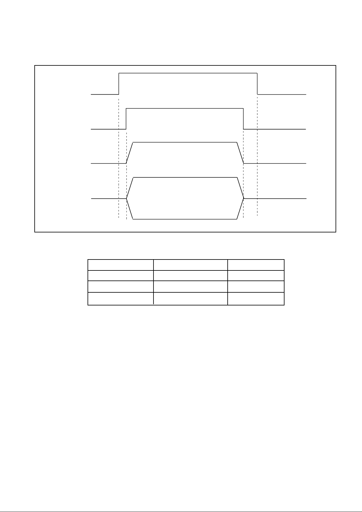
CONTROL WAVEFORMS
TX/RXB
PA_ON
Ramp_Cap
WL600C
CONTROL LOGIC
PA_Drive
RF output
Fig. 3 Transmit control waveforms
Control Line Logic ‘0’ Logic ‘1’
TX/RXB Receive Transmit
PA_ON PA off PA on
STDBYB Standby Active
7
Page 8
Page 9

http://www.mitelsemi.com
World Headquarters - Canada
Tel: +1 (613) 592 2122
Fax: +1 (613) 592 6909
North America Asia/Pacific Europe, Middle East,
Tel: +1 (770) 486 0194 Tel: +65 333 6193 and Africa (EMEA)
Fax: +1 (770) 631 8213 Fax: +65 333 6192 Tel: +44 (0) 1793 518528
Fax: +44 (0) 1793 518581
Information relating to products and services furnished herein by Mitel Corporation or its subsidiaries (collectively “Mitel”) is believed to be reliable. However, Mitel assumes no
liability for errors that may appear in this publication, or for liability otherwise arising from the application or use of any such information, product or service or for any infringement of
patents or other intellectual property rights owned by third parties which may result from such application or use. Neither the supply of such information or purchase of product or
service conveys any license, either express or implied, under patents or other intellectual property rights owned by Mitel or licensed from third parties by Mitel, whatsoever.
Purchasers of products are also hereby notified that the use of product in certain ways or in combination with Mitel, or non-Mitel furnished goods or services may infringe patents or
other intellectual property rights owned by Mitel.
This publication is issued to provide information only and (unless agreed by Mitel in writing) may not be used, applied or reproduced for any purpose nor form par t of any order or
contract nor to be regarded as a representation relating to the products or services concerned. The products, their specifications, services and other information appearing in this
publication are subject to change by Mitel without notice. No warranty or guarantee express or implied is made regarding the capability, performance or suitability of any product or
service. Information concerning possible methods of use is provided as a guide only and does not constitute any guarantee that such methods of use will be satisfactory in a specific
piece of equipment. It is the user’s responsibility to fully determine the performance and suitability of any equipment using such information and to ensure that any publication or
data used is up to date and has not been superseded. Manufacturing does not necessarily include testing of all functions or parameters. These products are not suitable for use in
any medical products whose failure to perform may result in significant injury or death to the user. All products and materials are sold and services provided subject to Mitel’s
conditions of sale which are available on request.
M Mitel (design) and ST-BUS are registered trademarks of MITEL Corporation
Mitel Semiconductor is an ISO 9001 Registered Company
Copyright 1999 MITEL Corporation
All Rights Reserved
Printed in CANADA
TECHNICAL DOCUMENTATION - NOT FOR RESALE
 Loading...