

Page 1
Features
● Complete CMOS, single chip, radio transceiver
controller
● Hardware implemented Communication Control
Block (CCB)
● Protocol independent design using external flash
memory
● Internal 8051 and external processor options
● Internal/external buffer and processor RAM
● Block power down facility
● PCMCIA/8bit processor host interface to buffer
RAM
● Up to 1Mbps/2 level or 2 Mbps/4 level operation
Ordering Information
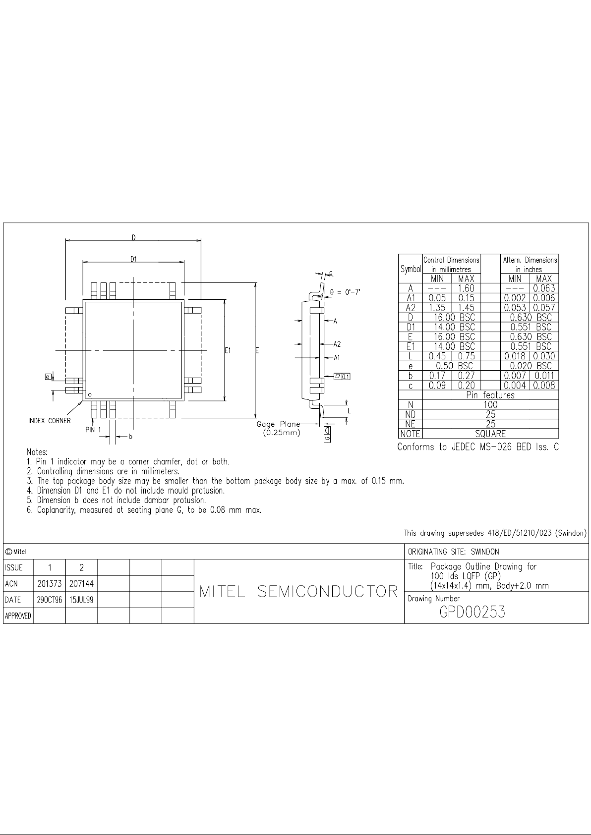
WL102B/IG/TP1R 100 pin package
WL102BC/PR/FP1R 144 pin package
The WL102B is a highly integrated CMOS wireless data
controller designed to dramatically reduce the cost of
radio data applications. It works with the WL600C RF IF
chip and WL800 synthesiser chip to offer a complete
solution for a frequency hopping, spread spectrum radio
in the 2.4 to 2.45GHz ISM band.
Its flexible design means that it can also be used in a
wide range of other applications using a range of "processor", protocols and additional memory options as well
as radios at other frequencies.
Related Documents
WL600C, WL800 and WL102B (DS4837) Datasheets
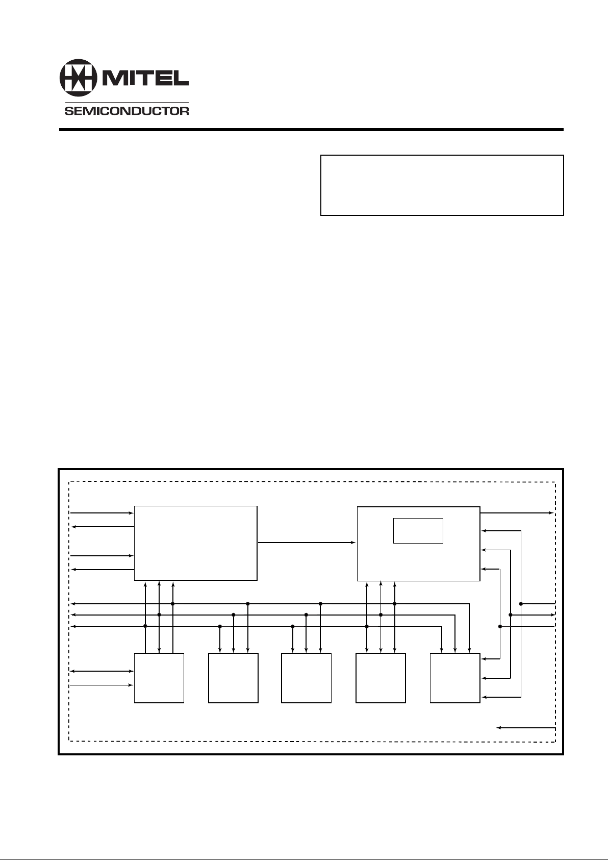
Communications
Control Block
Receive
Transmit
Status
Control
Address
Data
Control
Port Pins
Interrupt
Buffer RAM
6K4
8051
System RAM
4K
Counters
Power Down
Control
Attribute
Memory
Configuration
Control
Data
Address
Memory Control Block
Interrupt
DMA
WL102
Figure 1 WL102 Minimum configuration block diagram
WL102B
Wireless Data Controller
Advance Information
DS4582 - 3.0 July 1999
Page 2
2
WL102 Advance Information
HRDY
HD1
HD0
HA1
HREGB
HA2
HA3
HWAITB
HA4
HRESET
HA5
HA6
HA7
HA0
HWRB
HWEB
HRDB
HVdd
HGnd
HOEB
HCEB
HD7
HD6
HD5
HD4
CCAB
SYSCLK
SYSCLK_GND
AGnd
AVdd
RXD_L
RXD_LB
RXD_H
RXD_HB
THREEV
SWAKEUP / EPTCNT2
EPRDYB
ENIBRAMB
SPSENB
SRDB
SA10
CCEB
SD7
SD6
SD5
SD4
SD3
SD2
P1[5] / EPTCNT1
P1[3] / EPCINTR
HD2
HGnd
TEST0
TEST1
ENI8051B
RSSISTRB
MOD2LEVB
SVdd
SGnd
TXD_L
TXD_H / TXD
SYSCLK_D
RXD_D
P3[1] / EPMINTR
SYSCLK_X
CS_DATA / PWR_LOB
CS_CLK / ANT_SEL
CS_LOADB / LOADB
TX/RXB / RX/TXB
SVdd
SGnd
STDBYB
PA_ON
LCK_DETB
HVdd
132
456
798
101112
131514
161718
192120
222324
25
27
26
28
37
39
38
40
41
42
43
45
44
46
47
48
49
50
757473
29
30
31
33
32
34
35
36
515253545557565859606163626465666769687071
72
100
99
98
97
96
94
95
93
92
91
90
88
89
87
86
85
84
82
83
81
80
79
78
76
77
HD3
SA11
SA9
SA8
SA13
SVdd
SGnd
SA14
SWRB
SA15
SA12
SA7
SA6
SA5
SA4
SA3
SA2
SA1
SA0
SD0
SD1
SVdd
SGnd
P3[0] / EPSYSINC
EPRSTB
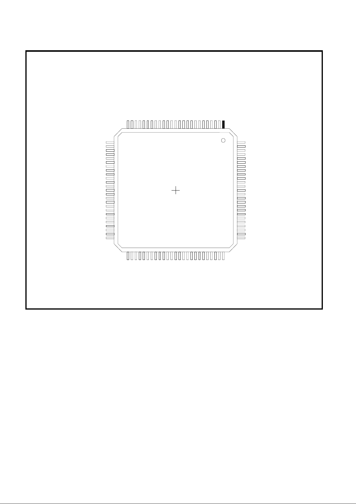
Fig.ure 2 100 Pin package
Page 3
3
Advance Information WL102
HRDY
HD1
HD0
HA1
HREGB
n/c
CSD6
HA2
HA3
CSD5
HWAITB
n/c
HA4
HRESET
HA5
CSD4
HA6
HA7
CSD3
HA0
HWRB
CSD2
HWEB
n/c
HRDB
HVdd
n/c
HGnd
CSD1
HOEB
HCEB
CSD0
HD7
HD6
HD5
HD4
HD3
SA11
SA9
SA8
EBA4
SA13
EBA5
SVdd
EBA6
SGnd
n/c
SA14
SWRB
EBD3
SA15
SA12
EBD2
SA7
SA6
EBD1
SA5
SA4
EBD0
SA3
EBA7
SA2
SA1
SA0
EBA8
SD0
SD1
EBA9
SVdd
SGnd
P3[0] / EPSYSINC
EPRSTB
CCAB
SYSCLK
SYSCLK_GND
AGnd
AVdd
EBA15
RXD_L
RXD_LB
RXD_H
RXD_HB
EBA14
THREEV
n/c
SWAKEUP / EPTCNT2
EBA13
EPRDYB
EBCEB
ENIBRAMB
EBWRB
EBRDB
SPSENB
EBA12
SRDB
SA10
CCEB
SD7
n/c
SD6
EBA11
SD5
SD4
EBA10
SD3
SD2
P1[5] / EPTCNT1
P1[3] / EPCINTR
n/c
HD2
HGnd
TEST0
TEST1
ENI8051B
n/c
EBD7
RSSISTRB
MOD2LEVB
EBD6
SVdd
SGnd
EBD5
TXD_L
EBD4
TXD_H / TXD
SYSCLK_D
EBA3
RXD_D
P3[1] / EPMINTR
SYSCLK_X
EBA2
CS_DATA / PWR_LOB
CS_CLK / ANT_SEL
EBA1
CS_LOADB / LOADB
n/c
TX/RXB / RX/TXB
SVdd
EBA0
SGnd
STDBYB
PA_ON
LCK_DETB
HVdd
132
456
798
101112
131514
161718
192120
222324
252726
282930
313332
343536
37
39
38
40
41
42
43
45
44
46
47
48
49
51
50
52
53
54
55
57
56
58
59
60
61
63
62
64
65
66
67
69
68
70
71
72
100
101
102
103
104
105
106
107
108
144
142
143
141
140
139
138
136
137
135
134
133
132
130
131
129
128
127
126
124
125
123
122
121
120
118
119
117
116
115
114
112
113
111
110
109
999897
969495
93
9291908889
878685
848283
818079
787677
757473
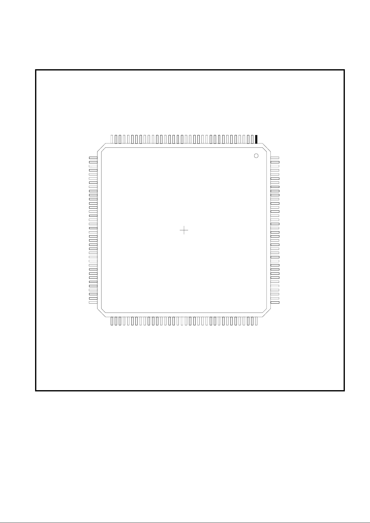
Figure 3 144 Pin package
Page 4

4
WL102 Advance Information
WL102 System Overview
The WL102 is a highly integrated digital wireless
transceiver controller suitable for controlling multiple
channel radios with data rates up to 1Mbit/s 2-level data or
2Mbit/s 4-level data. It has been designed to interface easily
with the WL600 and WL800 radio transceiver chips.
The use of low power synchronous on chip RAM and
selective power down of system blocks makes the WL102
ideally suited to power sensitive applications. Also the
WL102 can be operated from 3V or 5V supply rails with level
translation between the Host and MAC system built in to the
Host Interface. A minimum configuration of the WL102 with
a 64Kbyte external ROM for code storage makes it ideal for
small footprint applications, and the option of 100 pin or 144
pin TQFP 1mm packages make it suitable for PC-Card
applications.
The 100 pin package option allow the WL102 to be used in
the lowest cost solution. This includes all the internal blocks
of the WL102 hardware plus the option of an external
processor, to replace the internal 8051 core, and the
external system RAM and / or other peripherals on the
processor bus. The 144 pin package includes the 100 pin
features plus the option of using an external data buffer
RAM (up to 64K), to replace the internal 6.4K buffer RAM,
and the option of using the parallel synthesiser load pins the
are active in DE6003 mode of the CCB block, the Datasheet
DS4837 should be checked for further information on this
option.
It is envisaged that the WL102 hardware will allow the
development of a wireless network to the Media Access
Layer of the IEEE model for networking, with the addition
of an LLC layer providing the equivalent of the Data Link
layer of the ISO network model. In such a system the Host
interface buffer RAM would provide the boundary between
the LLC layer running on the Host and the MAC layer on the
internal WL102 8051 processor, or an optional external
MAC system processor.
Figure 1 shows the internal architecture of the WL102.
The WL102 provides an interface between a Host system,
such as a PC or PDA, which can be a PC-Card interface or
an 8 bit microprocessor bus, and an interface designed for
use with the DE6038 (WL600/WL800) radio transceiver.
The host interface provides a buffer and interrupt signalling
mechanisms between the Host and Mac system
processors. The MAC system processor is required to
provide the timing and control functions of Media Access
Control.
The Communications Control Block performs transmit and
receive operations directly to the buffer RAM so minimising
the load on the MAC system processor. A minimum
controller system configuration would be the WL102 plus
an external code memory device.
WL102 Hardware Blocks
System Processor
The WL102 contains an embedded processor, identical in
operation to an industry standard 8051 microcontroller,
with the exception that the internal data memory is
increased from 128 to 256 bytes.
System busses and strobes allow the 8051 to access the
full 64 Kbytes of external code memory. Internal
connections exist to the processor's two interrupt inputs,
and to the two timer inputs. Two I/O port pins are internally
connected to blocks within the WL102, whilst four of the
remaining I/O port pins are brought out to external pins,
including the serial receive and transmit port pins. Internal
address decoding provides access to the other blocks of
the device, with 36 Kbytes of the processor's 64 Kbytes
address range being unassigned and available for the
addition of external peripheral devices.
The 8051 demultiplexed address and data bus are
available externally to allow for the addition of extra
memory or other peripheral devices.
The 8051 is clocked at the internal system clock frequency
of 10MHz.
If additional processing power is required for a particular
application the WL102 may also be used with an external
processor instead of the internal 8051. This external
processor also accesses the WL102 blocks via the internal
address decode. Interrupt and Counter outputs are
brought to external pins and two control signals must also
be provided to the WL102.
Data RAM
The WL102 contains 4 Kbytes of static RAM which the
processor may use for variable storage etc. If additional
storage space is required, an external static RAM may also
be used, and mapped to an unused area of the WL102
memory map.
Page 5

5
Advance Information WL102
Memory Control Block
The memory Control Block allows access to the dual port
buffer used to communicate between the Host and WL102
system processes. The control logic of the buffer RAM
allows the Host to asynchronously read or write data at the
same time as the WL102 MAC system. To help arbitrate
access to this buffer space, a hardware semaphore
system is also included.
The WL102 contains 6784 bytes of low power buffer RAM
on chip. The 144-pin package option also allows for an
external (single port) SRAM to be used to increase the
buffer RAM space, up to 64Kbytes.
Host Interface
The Host Interface has been designed to be flexible
enough to allow its use from small microprocessor systems
to PC-Card slots. In a minimum configuration it uses only
4 address locations and a standard microprocessor type
read and write cycle. The interface provides access to the
Buffer RAM, which is accessible by both the Host and the
MAC systems simultaneously, and also to a control register which allows the Host to reset or interrupt the MAC
processor, and performs some other control functions on
the WL102.
Packets of data are typically buffered in the internal buffer
RAM before being transmitted or transferred from the MAC
system to the host.
The 8-bit interface is microprocessor and PCMCIA-compatible, with a separate dedicated RAM providing 255
bytes of attribute memory used for the configuration and
control of a PC Card. The host interface may be used by
any microprocessor-type interface which can supply two
bits of address, a chip enable signal, read/write strobes
and 8 bits of data, subject to timing requirements of the
WL102. The interface also provides an interrupt signalling
mechanism between the Host and MAC system as well as
some other control functions, such as a hardware semaphore and reset circuitry.
Communications Control Block
This block of the WL102 performs many of the functions
required for transmission and reception of data packets,
and interfaces directly to the radio transceiver. For power
sensitive applications the configuration registers can have
their clocks switched off once the initial configuration is
complete and for protocols which allow the transceiver to
sleep for periods of time, the clocks to the entire block can
be disabled via the Power Control register.
The CCB handles all the control signals for the radio and
can be configured for the timing required by the transceiver
being used. The CCB can directly access data stored in the
buffer RAM, via a DMA bus separate to the processor bus,
and once configured will finally handle a transmission or
reception, including CRC checking, address match, optional data scrambling (Bias suppression encoding) and
transfer of the data to/from the buffer RAM.
For shorter network management packets the MAC
system processor can directly read/write up to 64 bytes of
data from/to the CCB FIFO. The CCB generates maskable
interrupts to the MAC system processor at defined points
in the receive/transmit process to allow the processor to
perform any additional processing required to
succcccessfully complete the receive or transmit
sequence.
The Features of the CCB include:
● Transmission and reception of 2-level and 4-level
GFSK
bit streams at 625Kbps, 1Mbps and 2Mbps.
● Configurable Preamble/Frame word generation
and recognition
● Checksum generation and validation (CRC-16 and
CRC-32)
● Optional data coding schemes: bit-stuffing,
scrambling and bias suppression encoding (as
per draft IEEE 802.11)
● Dedicated data path for DMA transfer to and from
buffer RAM
● Address matching on received data packet
● Analysis of received signal for performing clear
channel assessment, including 16-bit countdown
timer
● 8 (maskable) interrupt sources to optimise
operation of the system software
● Automatic synthesiser channel loading for Rx/Tx
when using WL600/WL800
Page 6

6
WL102 Advance Information
Counters
The two 16-bit counters are provided which are configured
by setting a reload value. When enabled, the counters
decrement continuously at 10MHz, generating a terminal
count signal to the processor and automatically reloading
the reload value when the count reaches zero.
The terminal count outputs are internally connected to the
8051 timer inputs when using the internal 8051, and to
external pins when using an external processor.
Power Control
A power-down function is provided under the control of the
WL102 system. Power down enable signals are provided
to each major block; the clocks of the individual blocks
being disabled when the appropriate power down bit is set.
In addition, the internal processor's PCON register will
disable the 8051 core in the usual manner.
System Supply Voltages
The WL102 has two separate digital supply rails, allowing
for use in mixed 3V/5V systems. The host interface has its
own independent supply, whilst a second supply powers
the core of the WL102 and its interface to the memory and
radio transceiver subsystems. Both power supplies may
be operated at either 3 or 5 volts (nominal), with the
restriction that the host interface supply voltage must be
greater than or equal to the voltage powering the WL102
core and radio transceiver.
Manufacturing Enhancements
Radio Test Mode
The WL102 radio test mode of operation allows an
attached radio transceiver to be tested more easily in a
complete assembled unit. The mode is selected by
configuring the test mode pins. In this mode the usual
functions of the WL102 are suspended and the control and
status signals of the CCB radio interface are connected to
the pins of the Host interface, with the WL102 providing the
status signals back from the radio interface. The
comparators on the receive data stream are still used and
so the test system is provided with the digital version of this
radio output. In addition the operation of the CCB preamble
and frame word recognition can be tested, as well as the
clock recovery data stream.
MCB Execute Mode
This mode of operation is used to allow programming of the
external code memory if a re-programmable device is
used, via special software run on the Host. Using this
mode, the WL102's code memory is completely
reprogrammed regardless of its current state i.e. no 'bootblock' code is required in the WL102 system. This allows
complete radio modules to be manufactured without the
need for preprogramming the code memory. At final test
the MAC software image can be downloaded or test
software can be downloaded and used prior to the final
software.
This facility also allows the complete radio module to be
upgraded in the field or for diagnostic software to be
downloaded as necessary.
Page 7
Page 8
Page 9

M Mitel (design) and ST-BUS are registered trademarks of MITEL Corporation
Mitel Semiconductor is an ISO 9001 Registered Company
Copyright 1999 MITEL Corporation
All Rights Reserved
Printed in CANADA
TECHNICAL DOCUMENTATION - NOT FOR RESALE
World Headquarters - Canada
Tel: +1 (613) 592 2122
Fax: +1 (613) 592 6909
North America Asia/Pacific Europe, Middle East,
Tel: +1 (770) 486 0194 Tel: +65 333 6193 and Africa (EMEA)
Fax: +1 (770) 631 8213 Fax: +65 333 6192 Tel: +44 (0) 1793 518528
Fax: +44 (0) 1793 518581
http://www.mitelsemi.com
Information relating to products and services furnished herein by Mitel Corporation or its subsidiaries (collectively “Mitel”) is believed to be reliable. However, Mitel assumes no
liability for errors that may appear in this publication, or for liability otherwise arising from the application or use of any such information, product or ser vice or for any infringement of
patents or other intellectual property rights owned by third parties which may result from such application or use. Neither the supply of such information or purchase of product or
service conveys any license, either express or implied, under patents or other intellectual property rights owned by Mitel or licensed from third parties by Mitel, whatsoever.
Purchasers of products are also hereby notified that the use of product in certain ways or in combination with Mitel, or non-Mitel furnished goods or services may infringe patents or
other intellectual property rights owned by Mitel.
This publication is issued to provide information only and (unless agreed by Mitel in writing) may not be used, applied or reproduced for any purpose nor form par t of any order or
contract nor to be regarded as a representation relating to the products or services concerned. The products, their specifications, services and other information appearing in this
publication are subject to change by Mitel without notice. No warranty or guarantee express or implied is made regarding the capability, performance or suitability of any product or
service. Information concerning possible methods of use is provided as a guide only and does not constitute any guarantee that such methods of use will be satisfactory in a specific
piece of equipment. It is the user’s responsibility to fully determine the performance and suitability of any equipment using such information and to ensure that any publication or
data used is up to date and has not been superseded. Manufacturing does not necessarily include testing of all functions or parameters. These products are not suitable for use in
any medical products whose failure to perform may result in significant injury or death to the user. All products and materials are sold and services provided subject to Mitel’s
conditions of sale which are available on request.
 Loading...