

Page 1
W91570DN SERIES
DP
23-MEMORY TONE/PULSE DIALER WITH
AUTOREDIAL RTC AND LCD DISPLAY FUNCTIONS
GENERAL DESCRIPTION
The W91570DN series ICs are Si-gate CMOS ICs that provide the signals needed for either pulse or
tone dialing. They feature 23 number memories and a 16-digit LCD driver for displaying telephone
numbers and calling time. A real time clock is included to display the time of day. The W91570DN
series is fabricated using CMOS technology providing good performance in low voltage, low power
applications.
FEATURES
• Three by 32 digits for redial, save and mercury memory
• Twenty by 16 digits for one-touch direct or two-touch indirect repertory memory
• Uses 6 × 10 keyboard
• Pause, Pulse-to-tone (*/T) and flash can be stored as a digit in memory
• Minimum tone output duration: 87 mS
• Minimum intertone pause: 87 mS
• Tone/Pulse mode pin selectable
• Make/Break ratio pin selectable
• Dialing rate (10 or 20 ppS) pin selectable
• Pause time (2.0 or 3.6 Sec) selectable by keypad
• Flash break time (100, 300, or 600 mS) selectable by keypad
• Built-in 12 or 16-digit LCD driver (1/4 duty, 1/3 bias) selectable by mask option
• Built-in calling timer from [00:00] to [59:59]
• Uses 3.579545 MHz TV quartz crystal or ceramic resonator
• Uses 32768 Hz crystal as RTC frequency base
• Packaged in 80-pin plastic QFP with RTC
• Provides one-key-redial and auto-redial functions
• Switchable 24-hour clock or 12-hour clock with p.m. mode
• 0 or 9 dialing inhibition pin for PABX systems or long distance dialing lock out
• On-hook debounce: 150 msec in normal mode and 20 msec in lock mode
• Off-hook delay 300 mS in lock mode (i.e.
• First key-in delay: 300 msec in lock mode
• MUTE key for speech mute
• Cascade and mixed dialing allowed
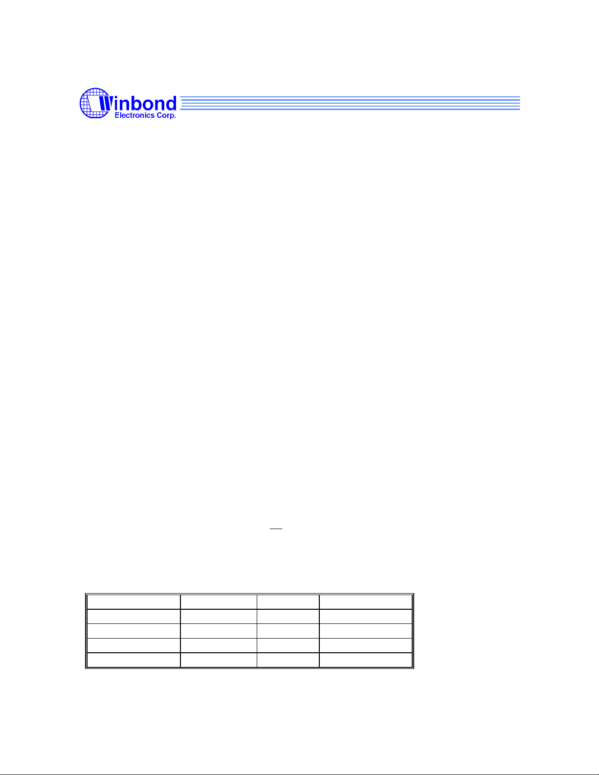
• The functions of the different dialers in the W91570DN series are shown in the following table:
PRODUCT NO. LCD DIGITS LOCK RTC BATTERY
W91572DNF 16
W91574DNF 16
W91576DNF 12
W91578DNF 12
will keep low for 300 mS while off hook)
√
√
√
√
1.5V
3V
1.5V
3V
Publication Release Date: May 1997
- 1 - Revision A2
Page 2
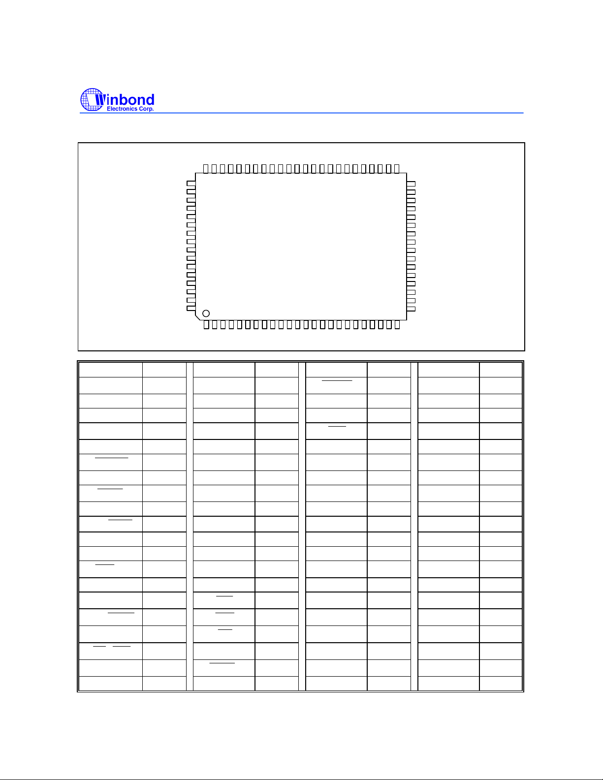
PIN CONFIGURATION
TESTL
XT2
KMUTE
TEST
1
LOCK
SET
XT1
MUTE
HKS
HFI
DP/C10
TEST
2
65
W91570DN SERIES
41
80
1
25
PIN NAME QFP-80 PIN NAME QFP-80 PIN NAME QFP-80 PIN NAME QFP-80
SEG29 1 COL2 21
41 SEG9 61
SEG30 2 COL3 22 APSET 42 SEG10 62
SEG31 3 COL4 23 XT2 43 SEG11 63
SEG32 4 COL5 24
44 SEG12 64
TEST 5 COL6 25 VLCD 45 SEG13 65
6 COL7 26 VRTC2 46 SEG14 66
KT 7 COL8 27 CN 47 SEG15 67
8 COL9 28 CP 48 SEG16 68
VDD 9 ROW1 29 COM1 49 SEG17 69
NC/
10 ROW2 30 COM2 50 SEG18 70
B/M 11 ROW3 31 COM3 51 SEG19 71
DTMF 12 ROW4 32 COM4 52 SEG20 72
RTC
13 ROW5 33 SEG1 53 SEG21 73
VSS 14 XT1 34 SEG2 54 SEG22 74
H/P MUTE 15
35 SEG3 55 SEG23 75
T/P
HFO 17
16
36 SEG4 56 SEG24 76
37 SEG5 57 SEG25 77
18 VRTC1 38 SEG6 58 SEG26 78
MODE 19
39 SEG7 59 SEG27 79
COL1 20 ARD 40 SEG8 60 SEG28 80
- 2 -
Page 3
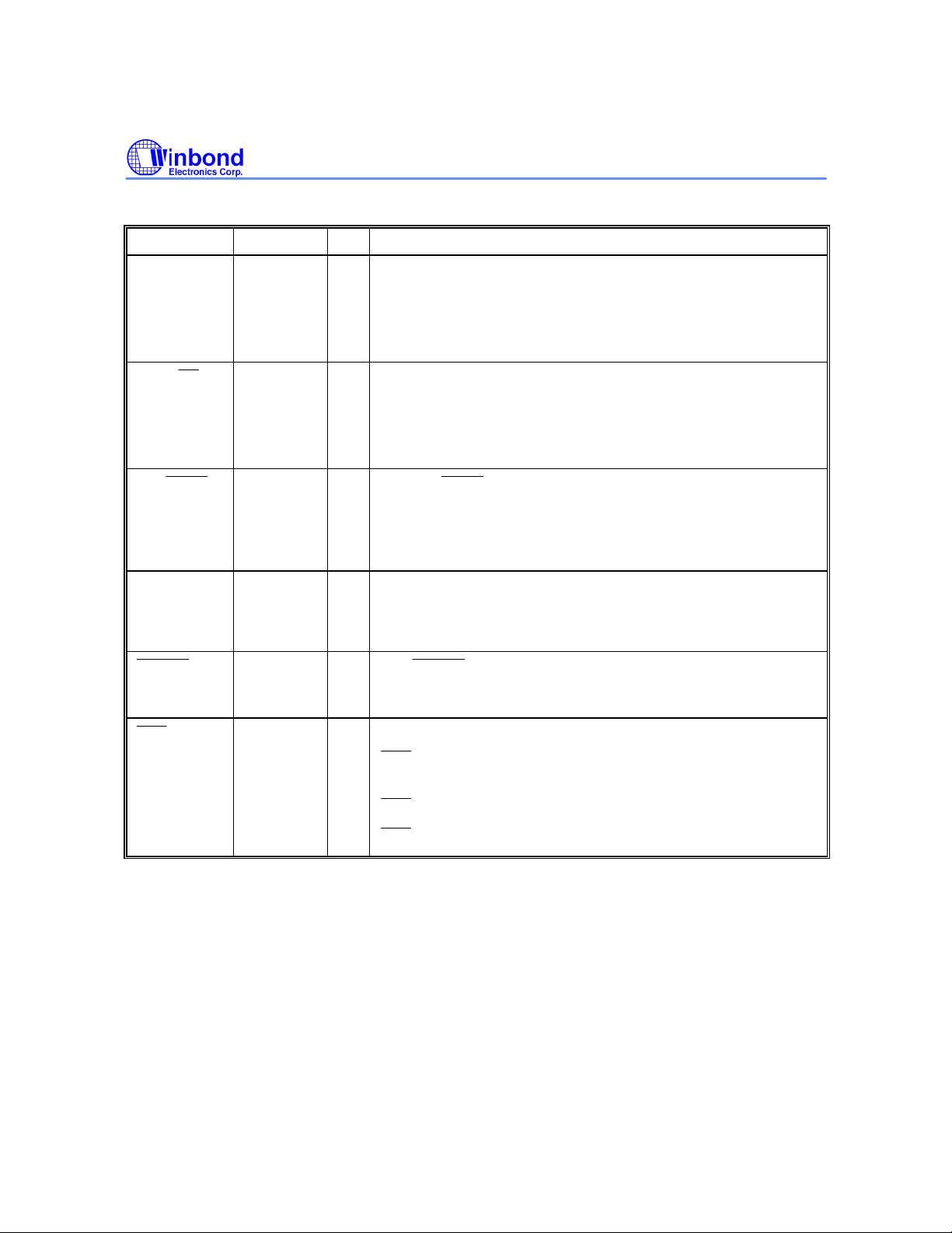
PIN DESCRIPTION
XT
MUTE
16
O
MUTE
KMUTE
KMUTE
HKS
HKS
HKS
HKS
SYMBOL PIN NO. I/O FUNCTION
W91570DN SERIES
Row,
Column
Inputs
XT1,
T/P
H/P MUTE 15 O The H/P MUTE is a conventional CMOS inverter output. During
29−33
and
20−28
34, 35 I,OA built-in inverter provides oscillation with an inexpensive
6 O
I
The keyboard inputs may be used with either the standard 6×10
keyboard, an inexpensive single contact (form A) keyboard or
electronic input.
A valid key entry is defined by a single row being connected to
a single column.
3.579545 MHz crystal or ceramic resonater.
The oscillator ceases when a keypad input is not sensed after
chip enable and dialing is finished. The crystal frequency
deviation is ±0.02%.
The T/P
output.
The output transistor is switched on low level during the dialing
sequence (both pulse and tone mode), one-key redial break,
auto redial break and flash break. Otherwise, it is switched off.
pulse dialing, one-key redial break, auto redial break, flash
break, hold, and mercury functions, this pin will output an active
high. It remains in a low state at all other times.
The
output transistor is switched on only during mute function.
Otherwise, it is switched off.
is a conventional CMOS N-channel open drain
is a CMOS N-channel open drain output. The
36 I Hook switch input.
= VDD or floating: On-hook state. Chip in sleeping mode,
no operation.
= VSS: Off-hook state. Chip enable for normal operation.
pin is pulled to VDD by internal resistor.
- 3 - Revision A2
Publication Release Date: May 1997
Page 4
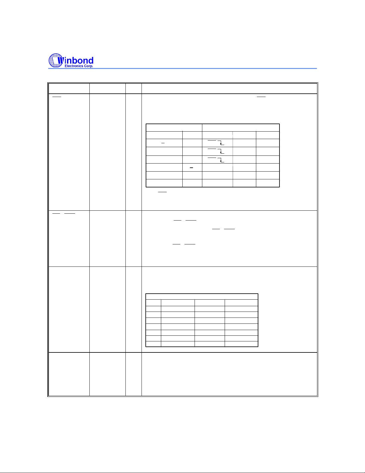
Pin Description, continued
HFI
HFI
HFI
DP/C10
C10
C10
C10
SYMBOL PIN NO. I/O FUNCTION
W91570DN SERIES
, HFO
37, 17 I,
Handfree control pins. A low pulse on the
O
the handfree control state.
input pin toggles
Status of the handfree control is listed in the following table:
CURRENT STATE
Hook SW.
On Hook High Low
Off Hook High
On Hook Off Hook Low Yes
Off Hook
Off Hook High On Hook High
The
pin is pulled to VDD by internal resistor.
HFO
Low
Low On Hook Low No
Input
HFI
HFI
HFI
NEXT STATE
HFO
High
Low Yes
Dialing
Yes
No
Yes
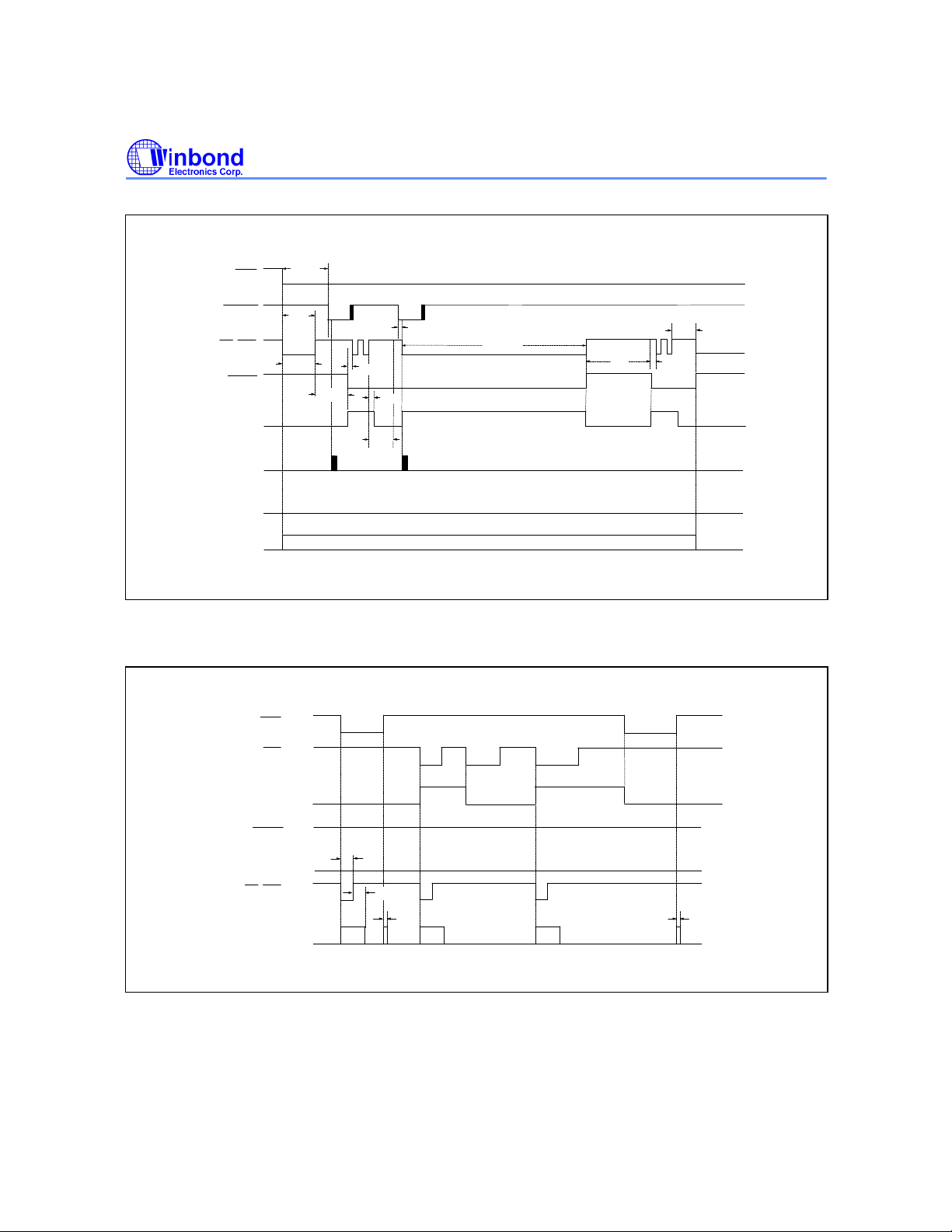
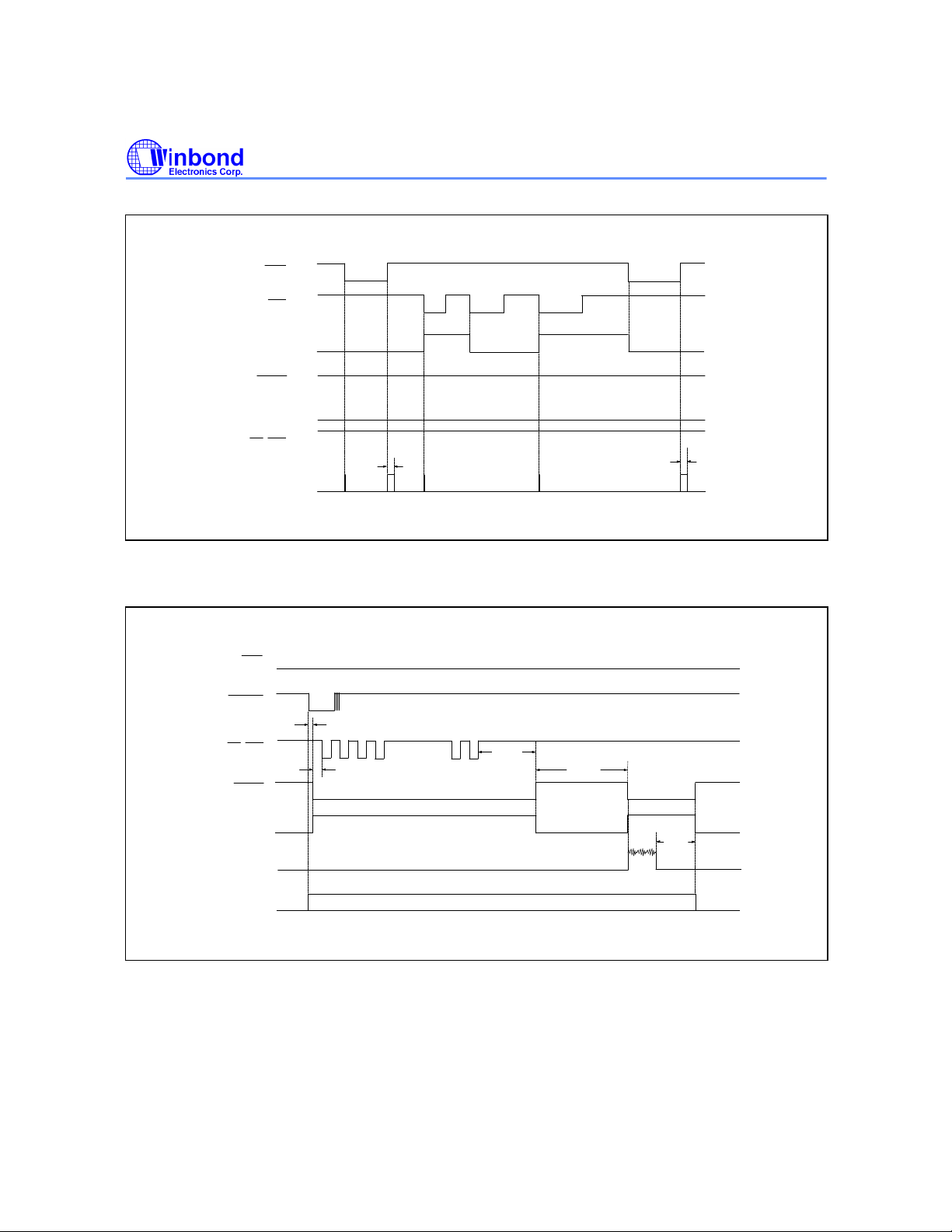
Detailed timing diagrams are shown in Figure 4(a), 4(b).
18 O This pin is a CMOS N-channel open drain output. The flash key
will cause DP/
mode. In lock mode, the DP/
to go active in either pulse mode or tone
keeps low for 300 mS during
off-hook delay time (If first off-hook occured after power-on
reset, the DP/
will keep high for 100ms then go low 200
mS. It will be recovered when first key-in was accepted). The
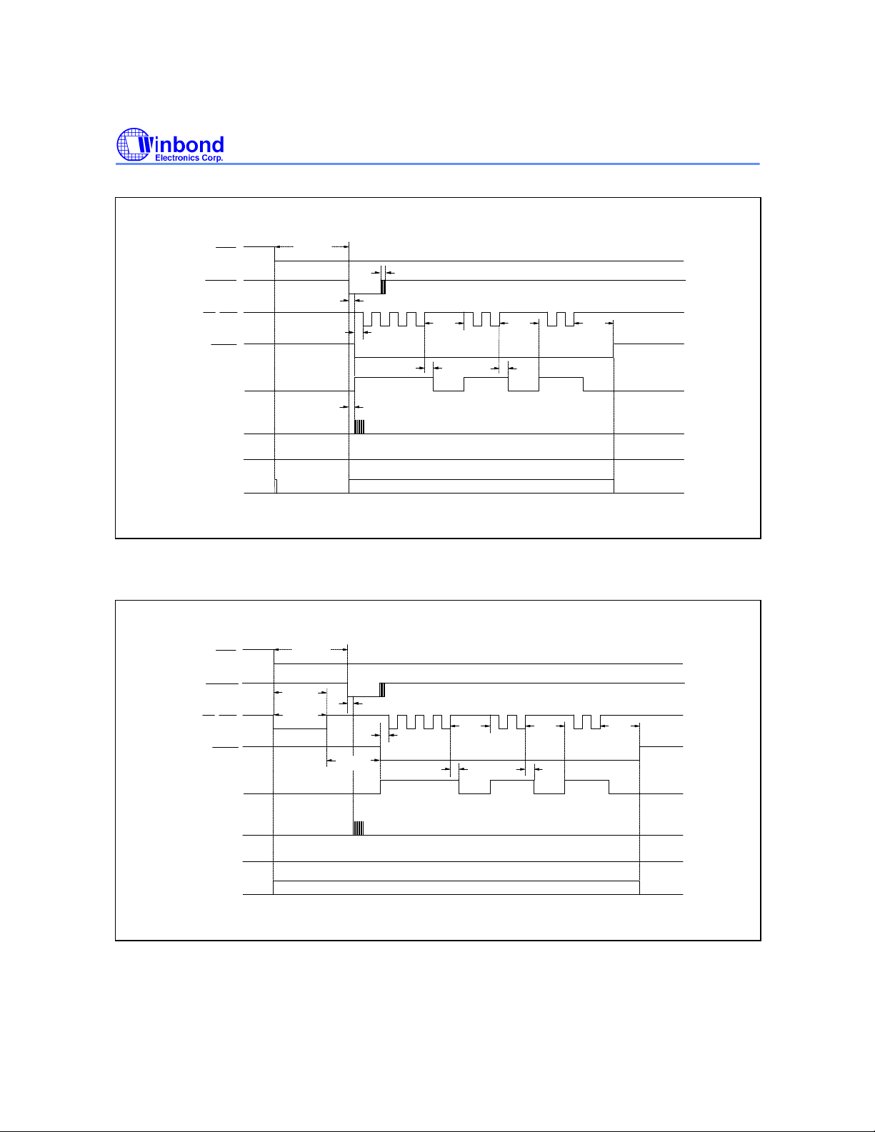
timing diagram is shown as Figure 1(a), 1(b), 1(c), 1(d).
DTMF 12 O In pulse mode, this pin remains in low state at all times.
In tone mode, it will output a dual or single tone. Detailed timing
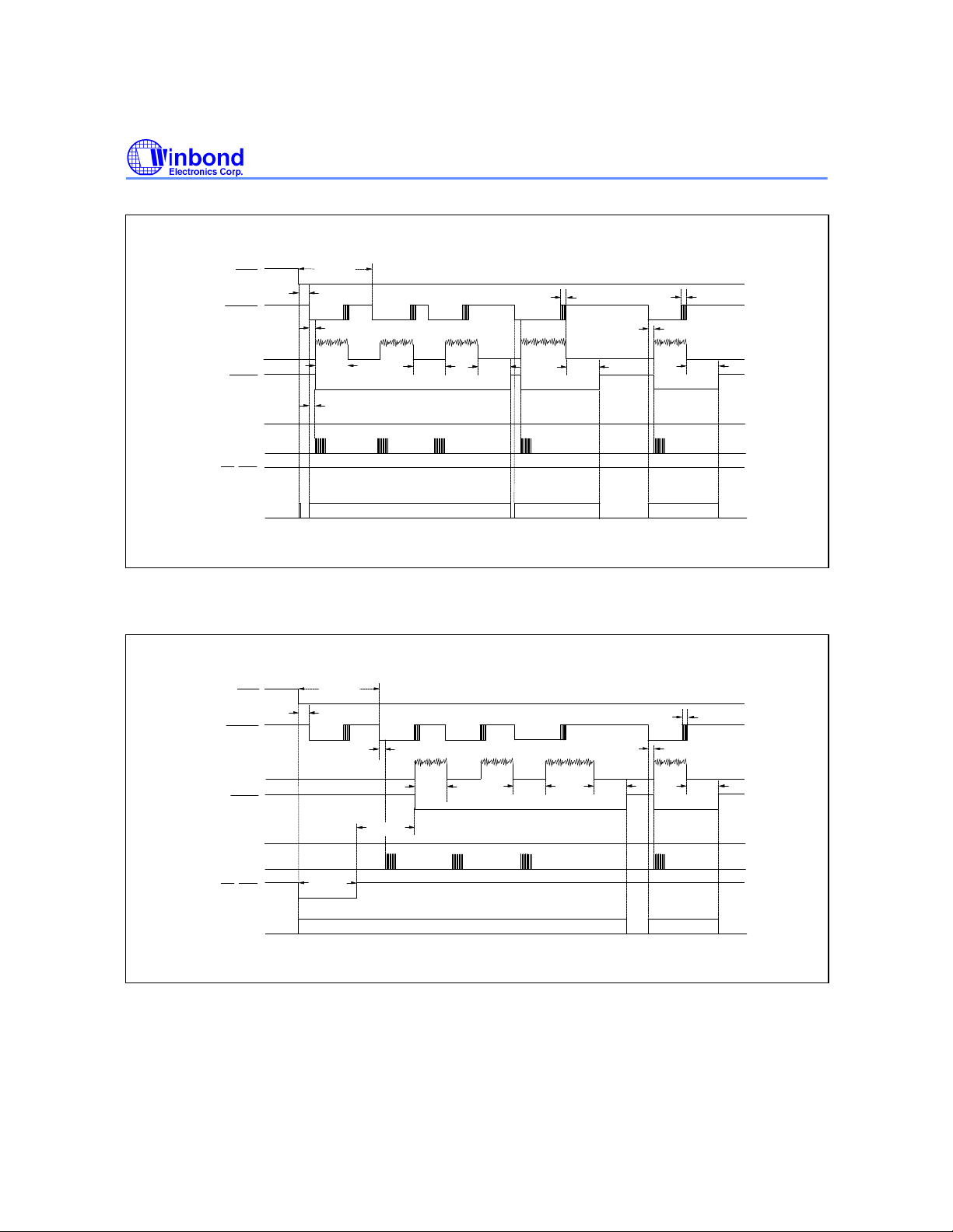
diagram for tone mode is shown in Figure 2(a), 2(b), 2(c), 2(d).
OUTPUT FREQUENCY
Specified Actual
R1
R2
R3
R4
C1
C2
C3
697
770
852
941
1209
1336
1477
699
766
848
948
1216
1332
1472
Error %
+0.28
-0.52
-0.47
+0.74
+0.57
-0.30
-0.34
MODE 19 I Pulling the mode pin to VSS places the dialer in tone mode.
Pulling the mode pin to VDD places the dialer in pulse mode
and the dialing rate is 10 ppS.
Floating the mode pin places the dialer in pulse mode and the
dialing rate is 20 ppS.
- 4 -
Page 5
Pin Description, continued
LOCK
LOCK
LOCK
XT2
SET
SET
SYMBOL PIN NO. I/O FUNCTION
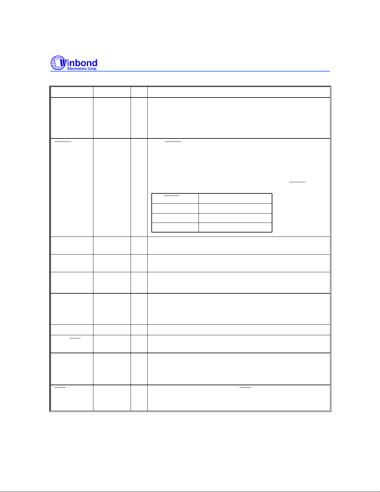
B/M 11 I Make:Break ratio select pin.
If B/M = VDD, the M/B ratio is 40:60.
If B/M = VSS, the M/B ratio is 33.3:66.7.
The B/M pin is pulled to VDD by internal resistor.
W91570DN SERIES
10
(for all lock
version)
I
The
pin is used to prevent "0" or "9" dialing under PABX
system long distance call control. When the first key input after
reset is "0" or "9", all the key inputs, including "0" or "9" key,
become invalid, and the chip generates no output.
The telephone is reinitialized by a reset.
The following table describes the functions of the
COM1 to
COM4
SEG1 to
SEG32
LOCK PIN
Floating
V
DD
V
SS
49 to 52 O COM1 to COM4 are the common signal output terminal for the
1/4 duty LCD.
53 to 80,
O SEG1 to SEG32 are the 16-digit segment signal outputs.
1 to 4
FUNCTION
Normal dialing
"0", "9" dialing inhibited
"0" dialing inhibited
VLCD 45 O Power supply pin for LCD driver.
A 0.1 µF capacitor is connected between VLCD and VSS.
CP, CN 48, 47
CP is the voltage control capacitor positive pin.
I
CN is the voltage control capacitor negative pin.
A 0.1µF capacitor is connected between these two pins.
pin:
VDD, VSS 9, 14 I Power input pins.
XT2,
43, 44 I,OA quartz crystal oscillator provides an RTC frequency time base
of 32.768 KHz.
VRTC1,
VRTC2
38, 46 I Either VRTC1 should be connected to a 1.5V battery
(W91572DN/576DN) or VRTC2 should be connected to a 3.0V
battery(W91574DN/578DN), which supplies the power source
for the RTC.
RTC
13 I
In the chip enable state, pulling
RTC set function on/off, when the set function is toggled on, the
RTC can be set using the "HOUR" and "MIN" keypads.
- 5 - Revision A2
RTC
to VSS toggles the
Publication Release Date: May 1997
Page 6
W91570DN SERIES
TEST
1,TEST
2,TESTL
Pin Description, continued
SYMBOL PIN NO. I/O FUNCTION
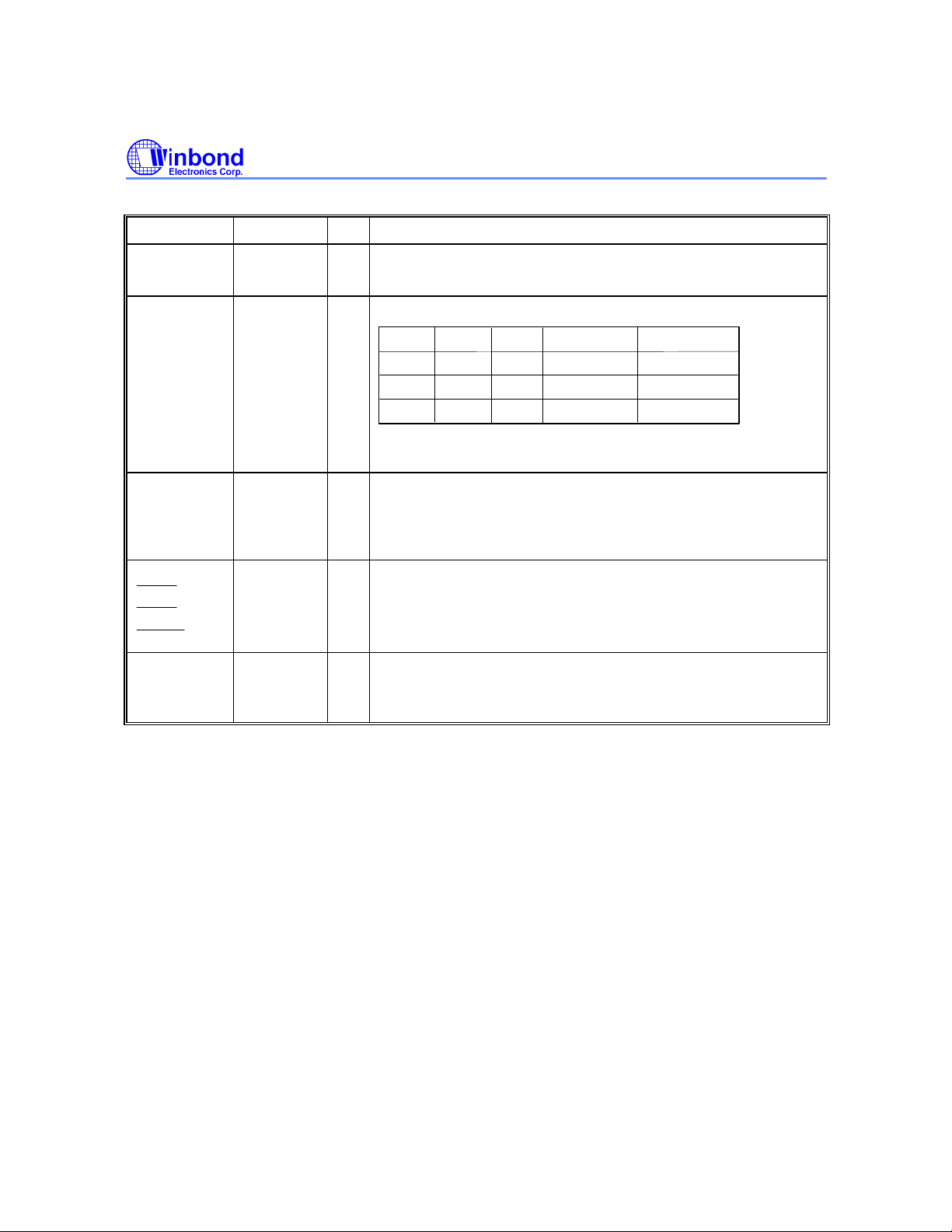
APSET 42 I If APSET = VDD or floating, 24-hour clock mode.
If APSET = VSS, 12-hour clock with p.m. mode.
ARD 40 I Auto redial function selection.
ARD
V
DD
V
SS
Floating
BREAK
4 secs
30 secs
4 secs
PAUSE WAIT INTERVAL
1 sec
1 sec
1 sec
25 secs
30 secs
-
REPEAT TIMES
10
10
1
When ARD is left floating, the one-key redial function is
enabled.
KT 7 O The key tone output is a conventional CMOS inverter.
The key tone is generated as any valid key pressed, as the KT
pin generates a 1.2 KHz square wave which keeps on 35 mS;
otherwise, it remain in low state.
TEST,
5, 8, 39,
I For testing only.
41
NC 10
(for
W91572/574/
W91576/578)
- No connection.
- 6 -
Page 7
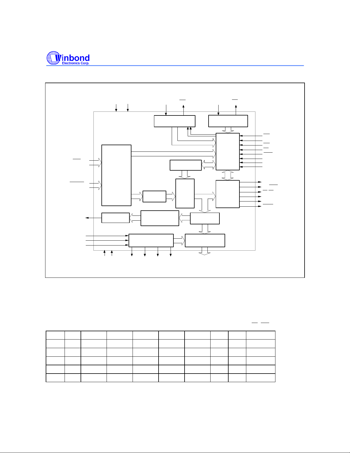
BLOCK DIAGRAM
C1C2C3C4C5C6C7C8C9
W91570DN SERIES
ROW
(R1 to R5)
COLUMN
(C1 to C9)
DTMF
V
LCD
V RTC1
V RTC2
V DD
KEYBOARD
INTERFACE
D/A
CONVERTER
CN
CP
SSV
LOCATION
ROW & COLUMN
PROGRAMMABLE
BACKPLANE SIGNAL
GENERATOR
COM2COM1 COM3
XT2
REAL TIME CLOCK
LATCH
COUNTER
GENERATOR
READ/WRITE
COUNTER
COM4
XT2
RAM
DATA LATCH
& DECODER
SEGMENT OUTPUT
DECODER
L.C.D.
GENERATOR
CONTROL
LOGIC
PULSE/
TONE
CONTROL
LOGIC
XT1
XT1
SYSTEM CLOCK
SET RTC
AP SET
HKS
HFI
LOCK
B/M
MODE
ARD
H/P MUTE
T/P MUTE
DP/C10
HFO
KT
KMUTE
FUNCTIONAL DESCRIPTION
Keyboard Operation
DP / C10
1 2 3 E HOUR M0 M5 M10 M15 HOLD1 R1
4 5 6 MUTE MIN M1 M6 M11 M16 HOLD2 R2
7 8 9 A2 SAVE M2 M7 M12 M17 MER R3
*/T 0 # R/P1 OKR M3 M8 M13 M18 A1 R4
F1 F2 F3 CHK TIM M4 M9 M14 M19 RTC R5
R/P2 - ICON12 ICON13 ICON14 ICON15 ICON16 VDD/VX/R6
Publication Release Date: May 1997
- 7 - Revision A2
Page 8
W91570DN SERIES
HFI
¡õ
HFI
¡õ
• E: Store digit
• MUTE: Mute key
• F1, F2, F3: Flash keys
• SAVE: Save memory key
• MER: Mercury memory key
• OKR: One-key redial function
• RTC: Real time clock toggle key
• HOLD1, HOLD2: Hold function keys
• R/P1, R/P2: Redial and pause function keys, P1 is 3.6 sec. and P2 is 2.0 sec.
• TIM: a. Display last calling time
b. Start and/or stop counting up calling time
• HOUR and MIN: Active when setting mode is operated after off-hook
• A1, A2: Indirect repertory memory dialing function keys, A1 for page 1 and A2 for page 2
If Lp = 0 to 9, Mp = M0 to M9, and Mq = M10 to M19, then
a. A1 + Lp (or Mp) the memory location M0 to M9 will be selected
b. A2 + Lp (or Mp) the memory location M10 to M19 will be selected
c. A1 (or A2) + Mq the memory location M10 to M19 will be selected
• */T: * in tone mode and P→T in pulse mode
• CHK: a. Check dialing number
b. Check last dialing time
c. Memory check (except mercury)
• ICON12, ..., ICON16: Keys reserved for user, can be toggled on any time when the chip is enabled
Notes: D1, ..., Dn, D1', ..., Dn': 0, ..., 9, ∗/T, #
R/P: R/P1 or R/P2
An: A1, A2
Ln: 0, ..., 9, map to indirect memory location 0, ..., 9
Mn: Direct memory location M0, ..., M19
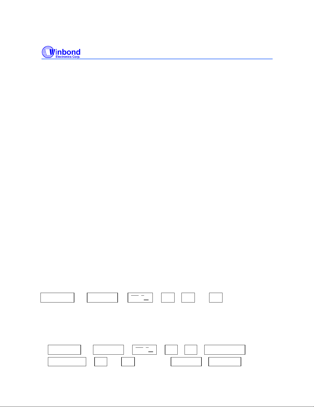
Normal Dialing
OFF HOOK (or ON HOOK &
1. D1, D2, ..., Dn will be dialed out.
2. Dialing length is unlimited, but redial is inhibited if the length oversteps 32 digits in normal dialing.
), D1 , D2 , ..., Dn
Redialing
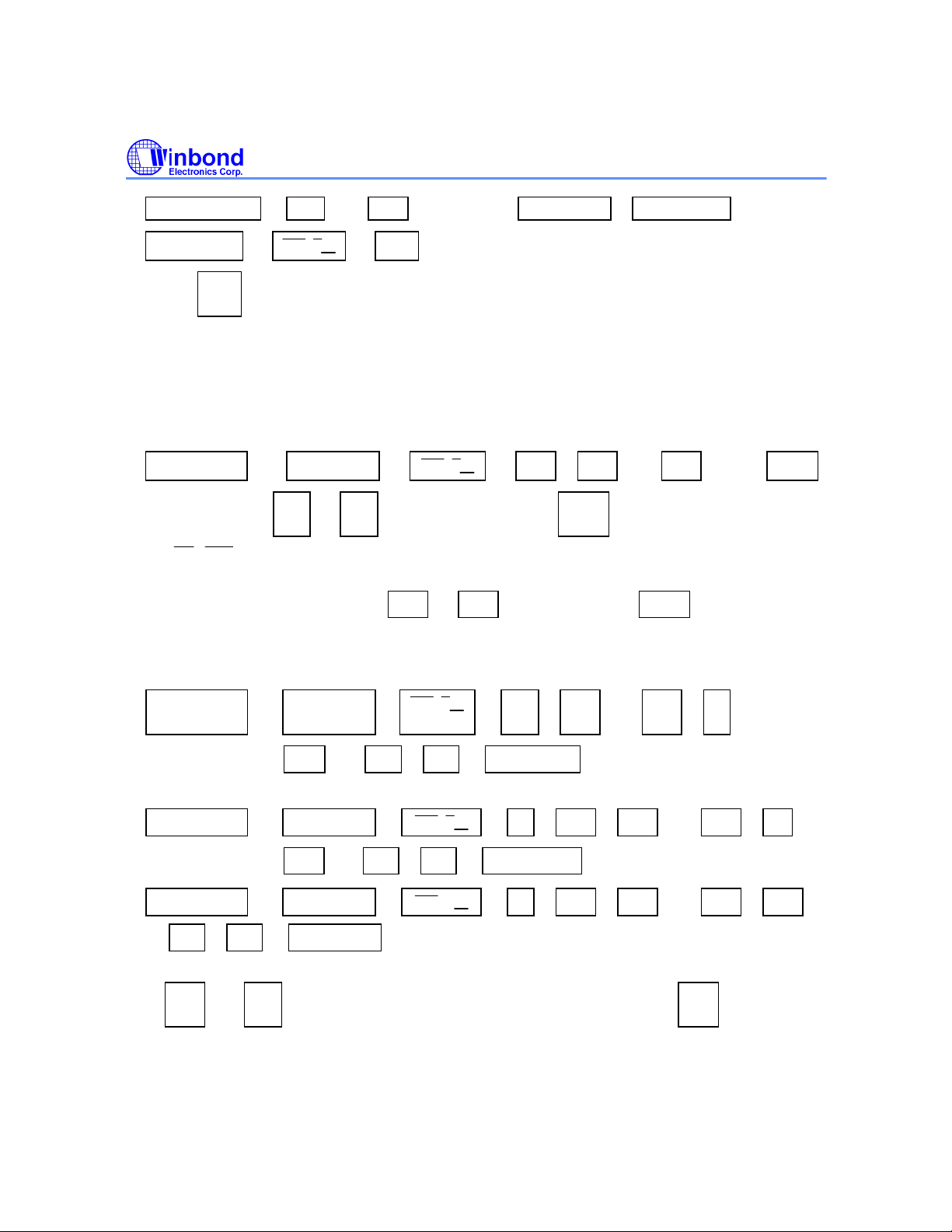
If ARD pin = floating, the one-key redial function is selected:
1. OFF HOOK (or ON HOOK &
), D1 , D2 , Check Memory (or
Number Store ), D3 , ..., Dn , Busy, ON HOOK , OFF (or
- 8 -
Page 9
W91570DN SERIES
HFI
¡õ
HFI
¡õ
C10
HFI
¡õ
HFI
¡õ
HFI
¡õ
Come HOOK
ON HOOK &
a.
The
b. The redial memory contents will be D3, ..., Dn.
c. Redial memory can be checked in memory check mode.
d. If redialing length oversteps 32 digits, the redialing function will be inhibited.
2. OFF HOOK (or ON HOOK &
a. If the dialingofD1 to Dn is finished, pressing the OKR key will cause the pulse output
pin DP/
automatically.
b. If the pulses of the dialed digits D1 to Dn have not finished, OKR will be ignored.
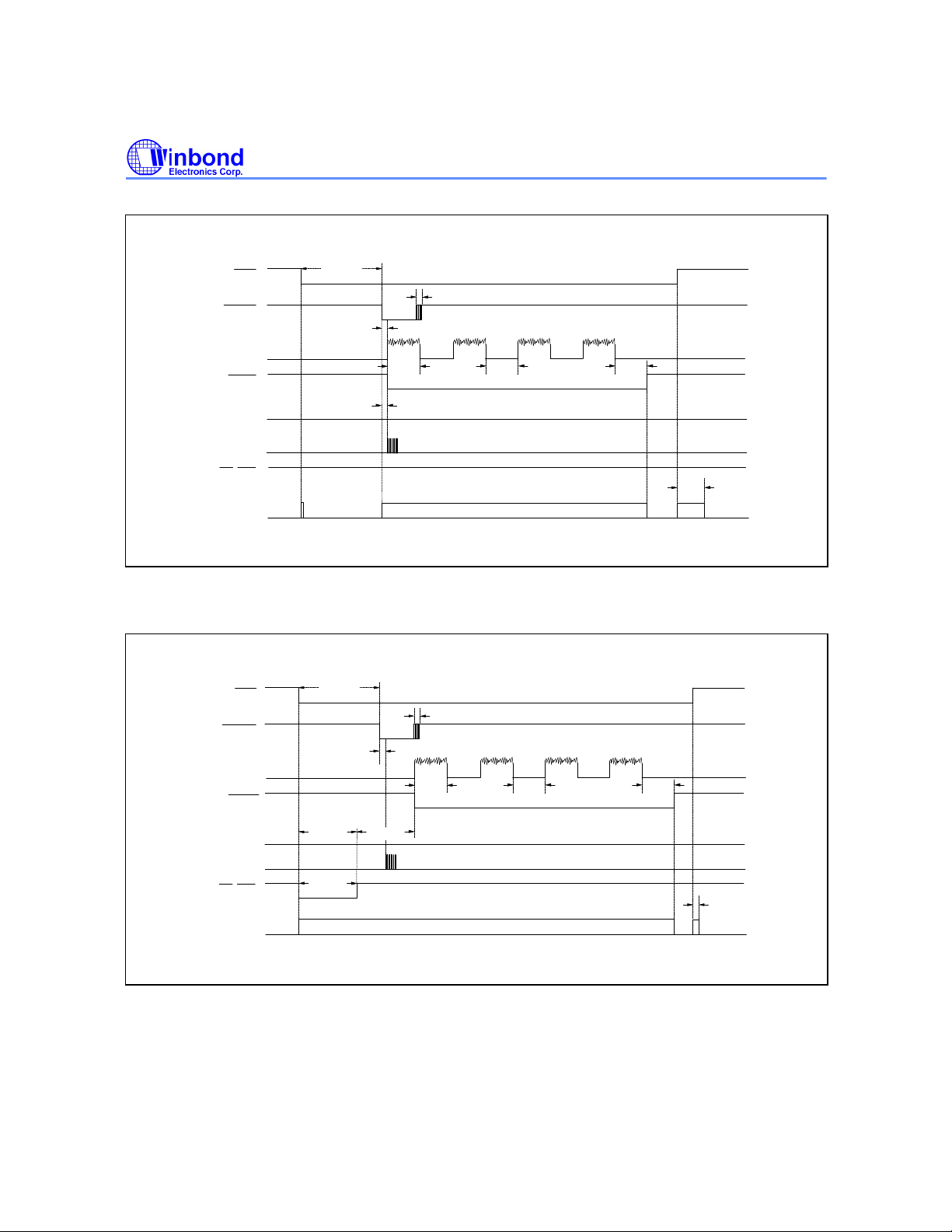
c. The one-key redialing function timing diagram is shown in Figure 3.
R/P key can execute the redial function only as the first dialing after off-hook; otherwise,
it
will invoke the pause
function.
to go low for 2.2 seconds break time and 0.6 seconds pause time will be added
), R/P
), D1 , D2 , ..., Dn , Busy, OKR
Number Entry
1. OFF HOOK (or ON HOOK
same as one time), Mn (or An , Ln ), ON HOOK
D1, D2, ..., Dn will be stored in memory location Mn (or Ln) and will be dialed out.
2. OFF HOOK (or ON HOOK
(could be skipped), Mn (or An , Ln ), ON HOOK
3. OFF HOOK (or ON HOOK
(or An , Ln ), ON HOOK
a. D1, D2, ..., Dn will be stored in memory location Mn (or Ln) but will not be dialed out.
b. R/P and */T keys can be stored as a digit in memory, in store
mode,
is the pause function key.
c. The store mode is released after the store function is executed or when the state of the hook
&
&
&
), D1 , D2 ,
), E , D1 , D2 , ..., Dn , E
), E , D1 , D2 , ..., Dn , Mn
Publication Release Date: May 1997
- 9 - Revision A2
Dn , E (many
...,
R/P
times
Page 10
switch changes is executed.
HFI
¡õ
HFI
¡õ
HFI
¡õ
HFI
¡õ
HFI
¡õ
W91570DN SERIES
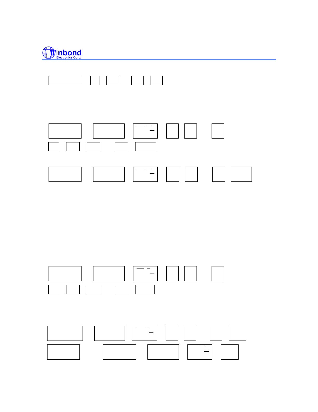
4. OFF HOOK ,
The redial content excluding memory dialing will be copied to memory location Mn (or Ln).
5. The first 16 digits will be stored into memory, if the key-in number over 16 digits.
E , Mn
(or An , Ln )
Save
1. OFF
HOOK
E , D1' , D2' , ..., Dn' , SAVE
D1', D2', ..., Dn' will be stored in save memory but will not be dialed out.
2. OFF
HOOK
a. If the dialing sequence D1, D2, ..., Dn has not finished, SAVE will be ignored.
b. If the sequence off hook, D1, D2, ..., Dn (dialing finish), SAVE, SAVE is keyed in, D1, D2, ...,
Dn
will be copied to save memory and D1, D2, ..., Dn will be dialed out again.
c. If the sequence off hook, D1, D2 (dialing finish), SAVE, D3, D4 (dialing finish), SAVE is keyed
in,
D1, D2 will be copied to save memory and D3, D4 will not be copied to save memory.
d. All above sequences will be displayed on LCD.
(or ON HOOK
(or ON HOOK
&
&
), D1 , D2 , ..., Dn ,
), D1 , D2 , ..., Dn , SAVE
CONVERSATION,
Mercury
OFF
HOOK
&
&
(or ON HOOK
), D1 , D2 , ..., Dn ,
CONVERSATION,
), D1 , D2 ,
&
- 10 -
Dn , MER ,
...,
), MER
1. OFF
HOOK
E , D1' , D2' , ..., Dn' , MER
D1', D2', ..., Dn' will be stored in mercury memory and display on the LCD, but will not be dialed
out.
2. MERCURY memory content = D1', D2', ..., Dn'
OFF HOOK (or ON HOOK
ON HOOK ,
a. The dialing sequence will be D1, D2, ... Dn, on hook, off hook, D1', D2', ..., Dn'.
(or ON HOOK
Come,
Page 11

W91570DN SERIES
b. The MER key can be used to execute the mercury function only when it is the first key-in in
dialing
mode after off-hook or first priority flash operation.
c. The contents of mercury memory will not be displayed on the LCD except for mercury mark.
d. If the sequence D1, D2, ..., Dn, MER, on-hook, off-hook, MER is keyed in, D1, D2, ..., Dn will not
be copied to mercury memory, D1', D2', ..., Dn' will be dialed out, and the mercury mark (icon 10)
will be blinking after off-hook. Detailed timing diagram is shown in Figure 5.
e. Mercury memory cannot be checked in memory check mode.
Publication Release Date: May 1997
- 11 - Revision A2
Page 12
Repertory Dialing
HFI
¡õ
HFI
¡õ
HFI
¡õ
HFI
¡õ
HFI
¡õ
HFI
¡õ
HFI
¡õ
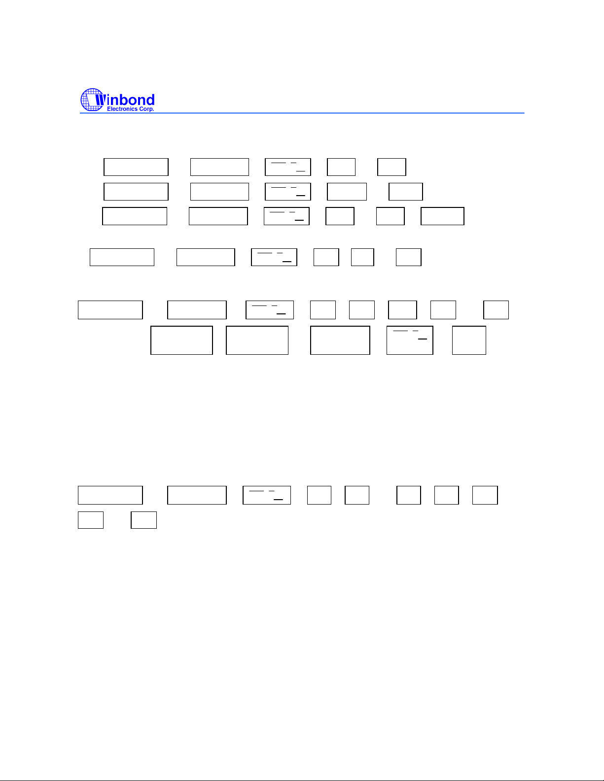
1. One-touch direct repertory dialing.
W91570DN SERIES
a. OFF HOOK (or ON HOOK
b. OFF HOOK (or ON HOOK
c. OFF HOOK (or ON HOOK
2. Two-touch indirect repertory dialing.
OFF HOOK (or ON HOOK
&
&
&
&
), Mn (or R/P )
), SAVE (or MER )
), Mn (or R/P ), SAVE
), An , Ln (or Mn )
Access Pause
OFF HOOK (or ON HOOK &
, Busy, Come, ON HOOK , OFF
1. The first R/P functions as a pause key and the second as a first key-in redial key.
2. The pause function can be stored in memory, and only one R/P key can be released to the user.
3. The pause function is executed in normal dialing, redialing, or memory dialing.
4. The pause duration of 2.0 or 3.6 seconds per pause is selected through the keypad.
5. The default pause duration is 3.6 seconds after power on.
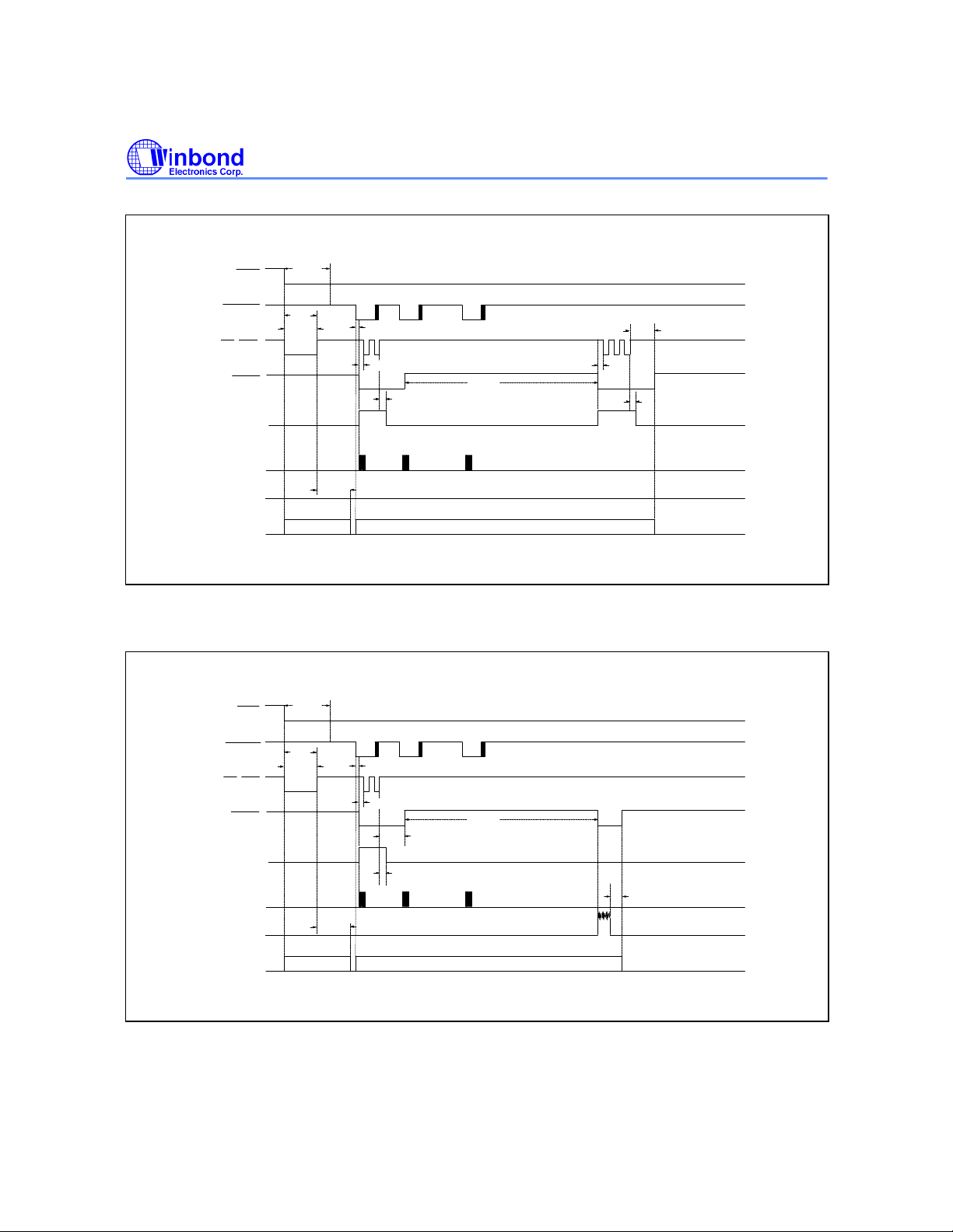
6. The pause function timing diagram is shown in Figure 6.
HOOK
), D1 , D2 , R/P , D3 , ..., Dn
(or ON HOOK
&
), R/P
Pulse- to-tone (*/T)
OFF HOOK (or ON HOOK &
D2' , ..., Dn'
1. If the mode switch is set to pulse mode, then the output signal will be:
D1, D2, ... Dn, Pause (2.0 sec/3.6 sec), D1', D2', ..., Dn'
(Pulse) (Tone)
2. If the mode switch is set to tone mode, then the output signal will be:
D1, D2, ... Dn, *, D1', D2', ..., Dn'
(Tone) (Tone)
3. The dialer remains in tone mode after the digits have been dialed out and can be reset to pulse
mode only by going on-hook.
4. The pause time of pulse-to-tone is default to 3.6 seconds.
5. The pulse-to-tone function timing diagram is shown in Figure 7.
), D1 , D2 , ..., Dn , */T , D1' ,
- 12 -
Page 13
Flash (F = F1, F2, F3)
HFI
¡õ
HFI
¡õ
HFI
¡õ
HFI
¡õ
HFI
¡õ
HFI
¡õ
HFI
¡õ
W91570DN SERIES
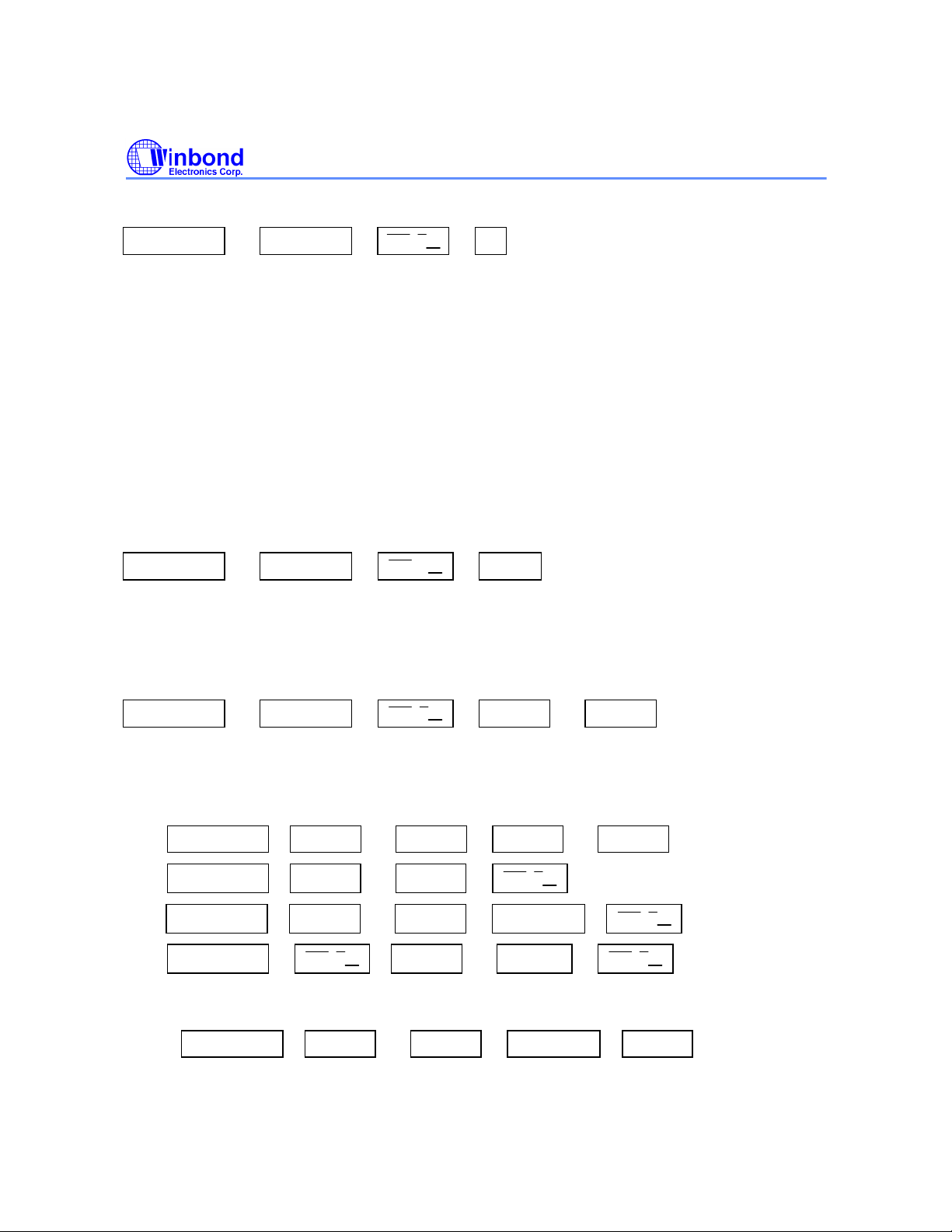
OFF HOOK (or ON HOOK
1. The dialer will execute a flash break time of 600 mS (F1), 300 mS (F2), or 100 mS (F3) and pause
time of 1S before the next digit (except flash key) is dialed out.
2. Flash keeps first priority in normal dialing but insert flash can be stored into memory when flash is
the first digit in memory. In this condition, only one flash key can be released to the user.
a. E, F1, D1, D2, D3, E, Mn then the digit stored in Mn will be F1, D1, D2, D3.
b. E, D1, F1, D2, D3, E, Mn then the digit stored in Mn will be D1, D2, D3.
c. F1, D1, D2, D3, E, Mn then the digit stored in Mn will be D1, D2, D3.
3. The system will return to the initial state after the flash pause time is finished.
4. Keyboard functions are inhibited when flash break is being executed.
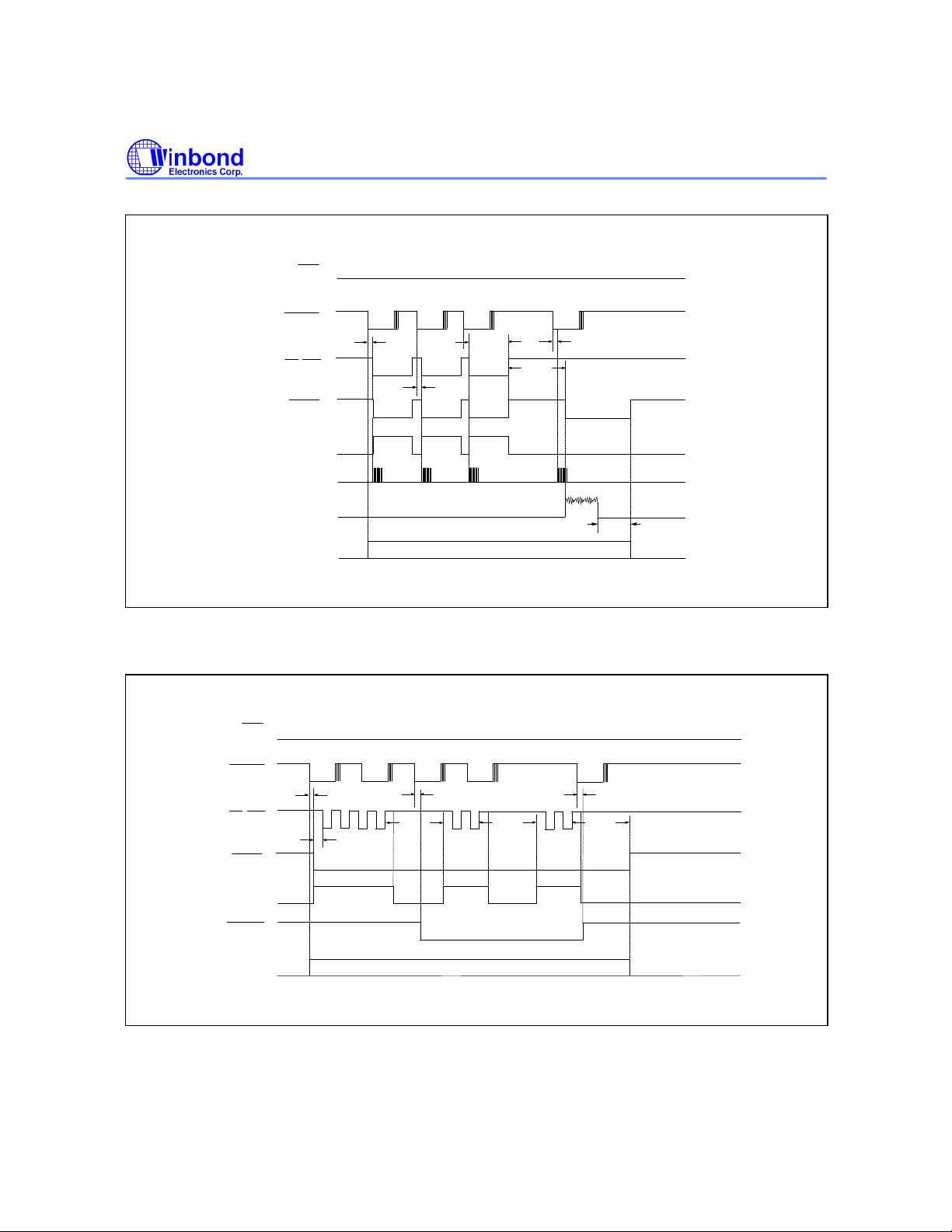
5. The flash timing diagram is shown in Figure 8.
&
), F
Mute
OFF HOOK (or ON HOOK
1. The MUTE is switched on and off by a toggle switch.
2. The function timing diagram is shown in Figure 9.
&
), MUTE
Hold Key
OFF HOOK (or ON HOOK
1. The hold function is toggled on and off by Hold1 or Hold2 key. When the hold function is toggled
on, the hold mark (icon 4) will be lit and all key-ins (except hold keys and icon keys) will be
ignored.
2. The following are examples of hold function toggled on and off:
a. OFF HOOK , HOLD1
b. OFF HOOK , HOLD1
c. OFF HOOK , HOLD1
d. ON HOOK &
3. Hold1 and Hold2 have the same function in off-hook state. The difference between Hold1 and
Hold2 are shown as follows:
a. If OFF HOOK , HOLD1
dialer will be off-line.
&
(or HOLD2
(or HOLD2
(or HOLD2
, HOLD1
(or HOLD2
), HOLD1 (or HOLD2 )
), HOLD1 (or HOLD2 )
),
), ON HOOK ,
(or HOLD2 ),
- 13 - Revision A2
), ON HOOK , HOLD1 is entered, then the
Publication Release Date: May 1997
Page 14
W91570DN SERIES
HFI
¡õ
HFI
¡õ
HFI
¡õ
SET
¡õ
SET
¡õ
SET
SET
SET
HFI
¡õ
HFI
¡õ
If OFF HOOK , HOLD1
(or HOLD2
), ON HOOK , HOLD2 is entered, then
the dialer stay at hold function.
b. If ON HOOK &
, HOLD1
(or HOLD2 ), HOLD1 is entered, then
the dialer will be off-line.
If ON HOOK &
, HOLD1
, (or HOLD2 ), HOLD2 is entered, then
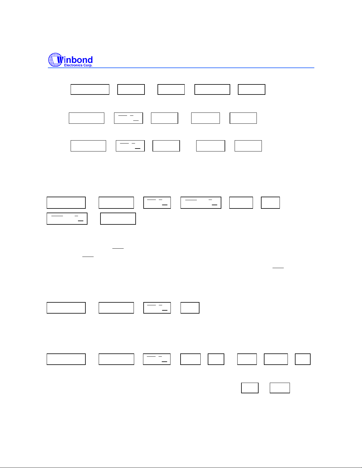
the dialer stay at hold function.
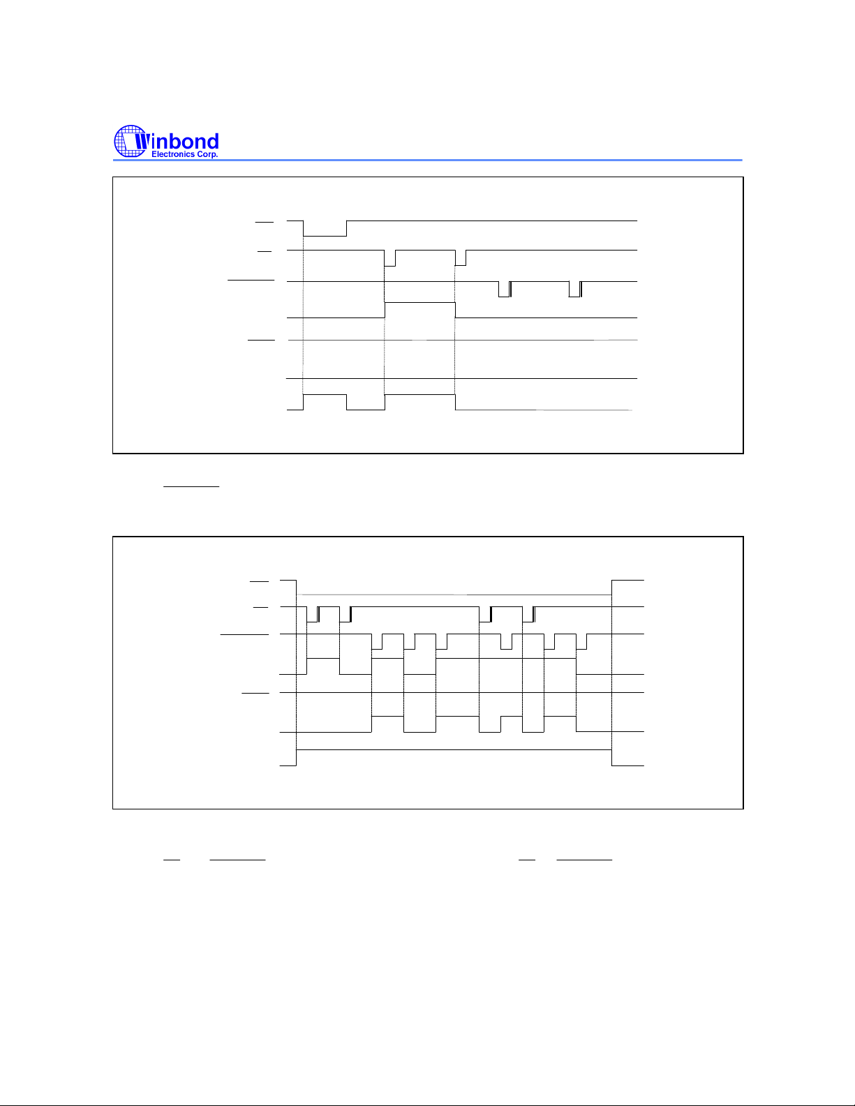
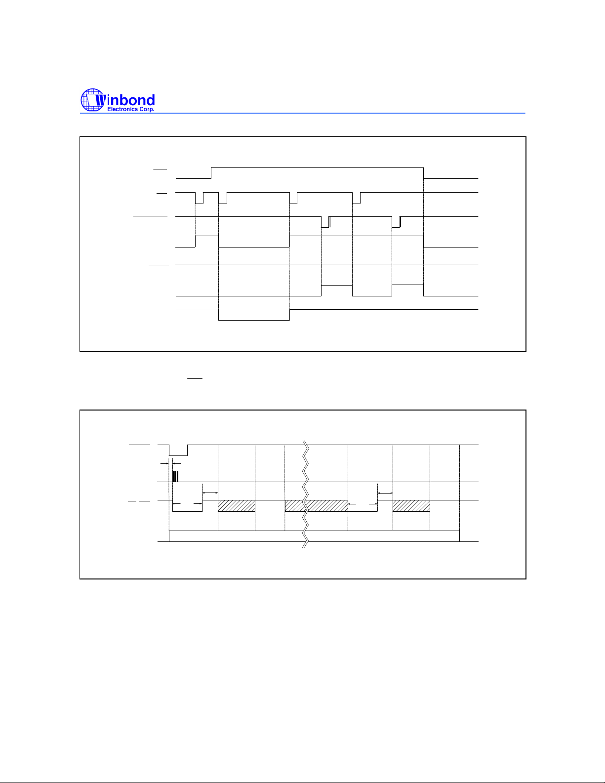
4. The function timing diagram is shown in Figure 10(a), 10(b), 10(c).
Adjusting Time Setting
OFF HOOK (or ON HOOK &
RTC
(or ON HOOK )
1. Only HOUR and MIN keys are valid in set RTC mode.
2. Hours and minutes count forward as long as the HOUR or MIN key is pressed.
3. The on/off function of
toggle off
RTC function.
RTC is toggled, and the dialer will go back to a previous state after the
),
RTC
, HOUR , MIN ,
4. If the dialing sequence D1, D2, ..., Dn (including flash and pause) has not finished,
'RTC' key pressed) will be ignored.
RTC Display Mode
OFF HOOK (or ON HOOK &
1.The real time clock display mode can be toggled on and off by RTC key.
2. The icon display will not be changed when enter RTC display mode and set RTC mode.
), RTC
Check Key
OFF HOOK (or ON HOOK &
, ..., etc.)
The redial (or memory) content will be displayed on the LCD when either R/P or OKR
is keyed in.
), CHK , R/P (or OKR , SAVE , Mn
- 14 -
RTC (or
Page 15
Auto Redial
HFI
¡õ
HFI
¡õ
HFI
¡õ
HFI
¡õ
HFI
¡õ
HFI
¡õ
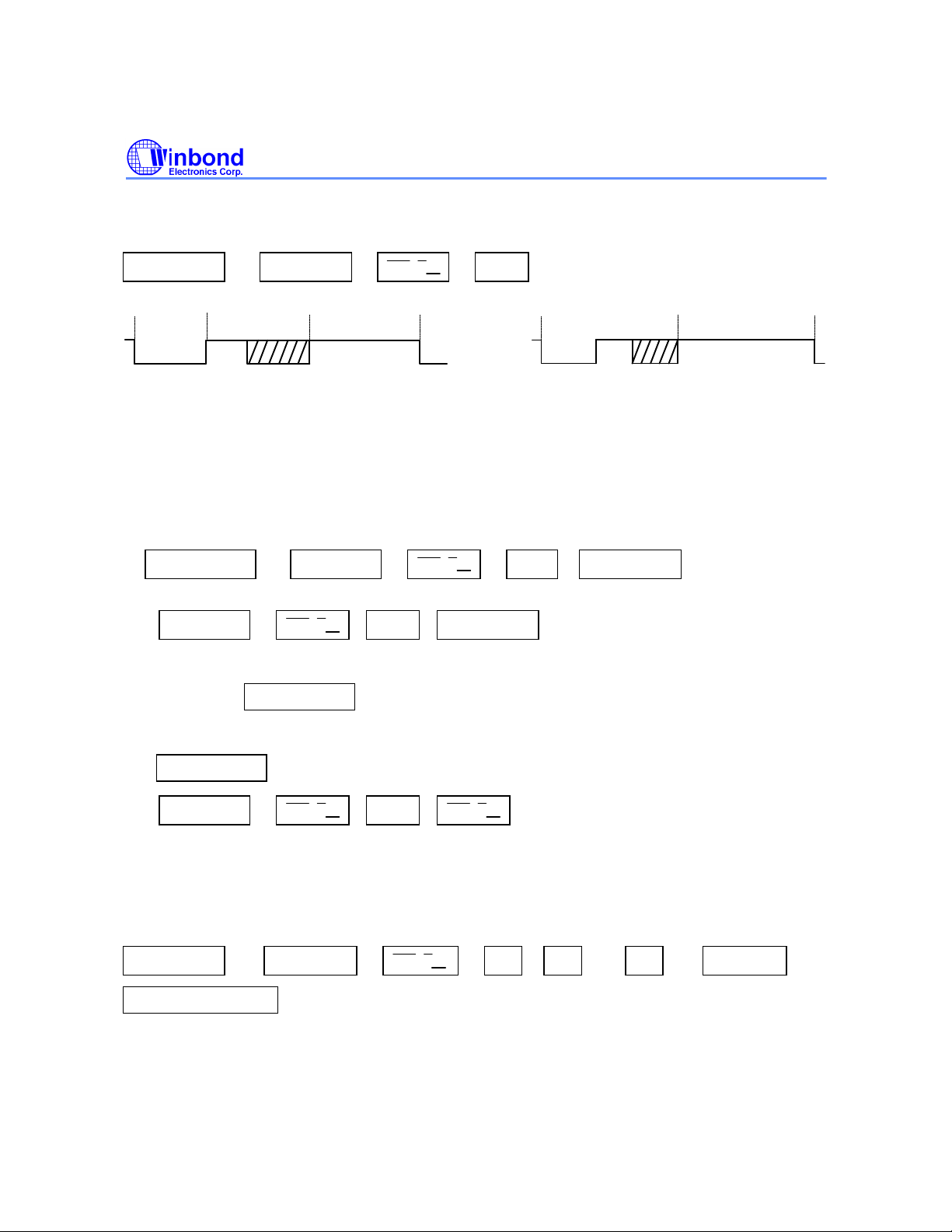
If ARD pin = VDD or VSS, the auto redial function is selected:
W91570DN SERIES
OFF HOOK (or ON HOOK &
Time Zone (A)
Time Zone (B)
Time Zone (C)
waiting interval
Break
Time Time
Pause
Auto dialing
), OKR
repeat till
n-1 times.
Break
Time
Time Zone (A)
Pause
Auto dialing
Time
Time Zone (B)
waiting interval
1. During time zone (B) the keypads are inhibited, and in time zone (A), (C) the auto redial can be
interrupted by pressing any keypad or by going off-hook.
2. The visible dialing number will be blinking during the waiting time interval.
3. If OKR is the first key-in after off-hook or handfree then the first break and pause time will be
ignored.
4. The following show examples to interrupt auto redial function:
OFF HOOK
(or ON HOOK
&
), OKR , Any Keypad (at break time and
waiting interval)
5. If ON HOOK &
, OKR
, OFF HOOK
a. When in time zome (A) or (C), the auto-redial function will be interrupted and changed to hook
mode after OFF HOOK
b. When in time zome (B), the auto-redial functiion will continue and changed to hook mode after
OFF HOOK
6. If ON HOOK &
, OKR
,
(any time) is entered, the dialer will be off-line.
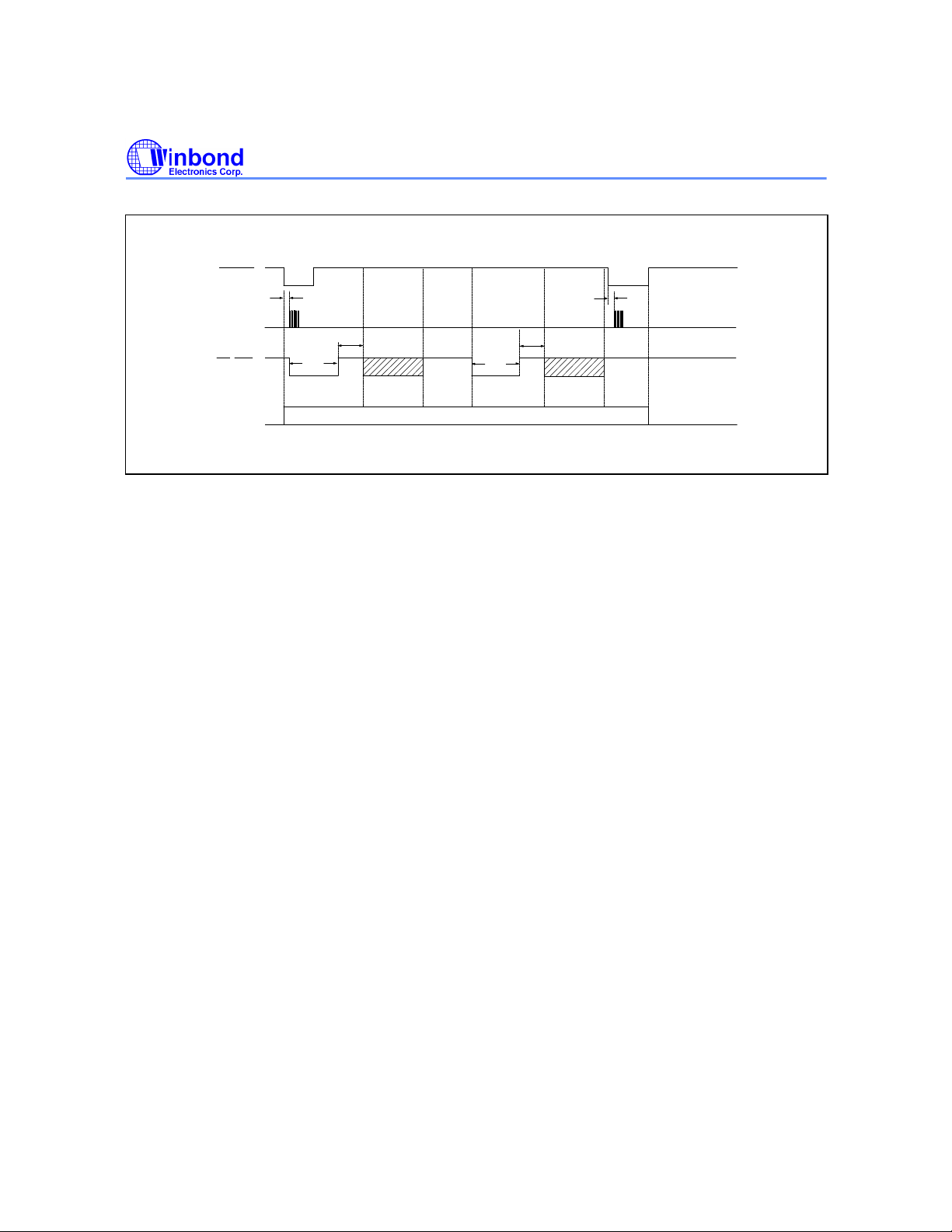
7. The auto redial function timing diagram is shown in Figure 11(a), 11(b).
8. The calling time will auto-count when the auto-redial function is interrupted in break time zone (A)
and (C).
TIM
OFF HOOK (or ON HOOK &
Repertory dialing 1 ), CONVERSATION
1. If no key is pressed after dialing is finished, the LCD will display counting time after 6 seconds.
2. If the dialing sequence D1, D2, ..., Dn has not finished, TIM will be ignored.
3. The timer will be initialized by flash and auto redial.
), D1 , D2 , ..., Dn (or Redialing or
Publication Release Date: May 1997
- 15 - Revision A2
Page 16
W91570DN SERIES
Cascaded and Mixed Dialing
Cascaded Dialing
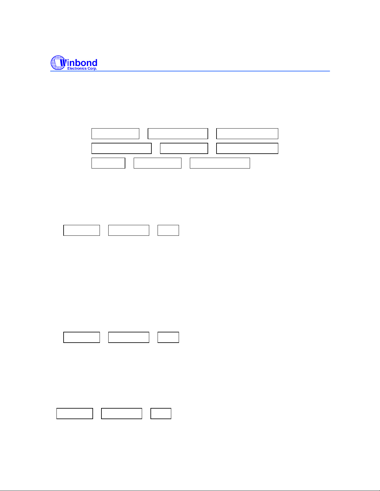
1. Definition of cascaded dialing:
In cascaded dialing, a new sequence may be pressed before the previous sequence has been sent
out completely. The following are examples of cascaded dialing:
Example 1: Normal dialing + Repertory dialing 1 + Repertory dialing 2 +...
Example 2: Repertory dialing 1 + Normal dialing + Repertory dialing 2 +...
Example 3: Redialing + Normal dialing + Repertory dialing 1 +...
2. Normal dialing, redialing, or repertory dialing as represented by each rectangle above is treated as
one sequence.
3. At most 64 digits are allowed in cascaded dialing, but there is no limitation on the number of
sequences.
4. The content of cascaded dialing may a combination of normal dialing, redialing, and repertory
dialing. Redialing is vaild only as the first key-in, however.
5. If ON HOOK , OFF HOOK
described in the above examples will be dialed out only if there are not more than 32 digits. If the
sequence exceeds 32 digits then the redialing is inhibited.
Mixed Dialing
1. Definition of mixed dialing:
The examples of cascaded dialing given above are also examples of mixed dialing except that in
mixed dialing a new sequence may be accepted only when the previous sequence has been dialed
out completely.
2. There is no limitation on the number of digits and sequences in the mixed dialing.
3. The content of mixed dialing may be a combination of normal dialing, memory dialing, or one-key
redialing.
4. If ON HOOK , OFF HOOK
described in the above examples will be dialed out only if the total number of digits does not
exceed 32. If the total exceeds 32 digits, then redialing is inhibited.
, OKR
, OKR
is entered, then the cascaded dialing sequence
is entered, then the mixed dialing sequence
Combining of Cascaded and Mixed Dialing
1. Cascaded dialing and mixed dialing may be combined, and each follows the rules described
above.
2. To apply redialing to combinations of cascaded and mixed dialing:
ON HOOK , OFF HOOK
digits does not exceed 32. Otherwise, the redialing is inhibited.
, OKR
then redialing will be executed only if the total number of
- 16 -
Page 17
W91570DN SERIES
HKS
HKS
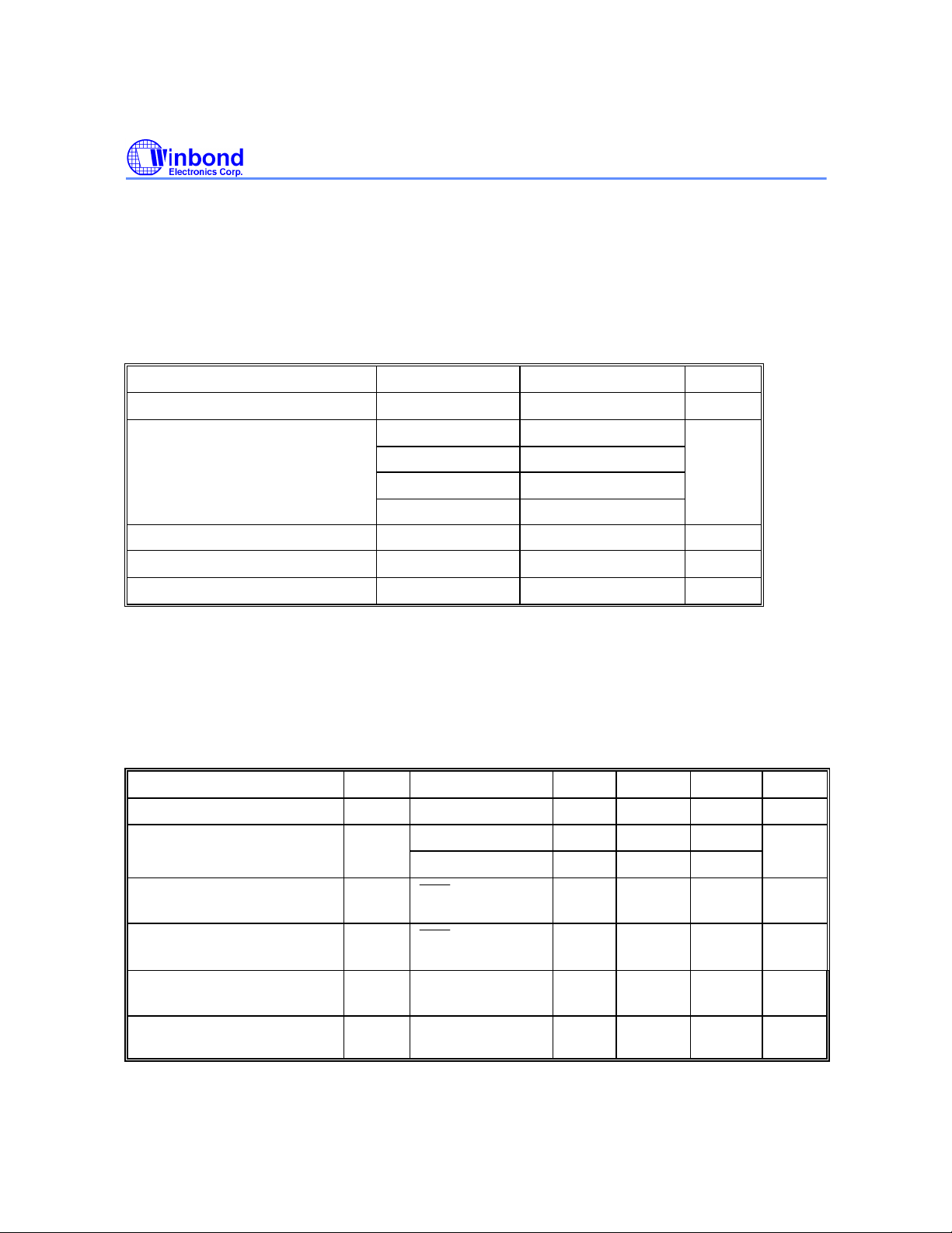
3. If there had been n cascaded sequences with a total of 60 digits dialed, then for the (n+1)th
cascaded sequence, one 4-digit normal dialing sequence or one complete repertory dialing
sequence (length up to 32 digits) can be dialed. The (n+2)th sequence will not be accepted for
cascaded dialing.
4. After a total of 64 digits of cascaded dialing have been completed, mixed dialing can be added.
ABSOLUTION MAXIMUM RATINGS
PARAMETER SYMBOL RATING UNIT
DC Supply Voltage
Input/Output Voltage VIH VDD + 0.3
Power Dissipation PD 120 mW
Operating Temperature TOPR -0.5 to +70
Storage Temperature TSTG -55 to +125
VDD−VSS
VIL
VOL
VOH VDD + 0.3
-0.3 to +7.0 V
VSS − 0.3
VSS − 0.3
°C
°C
Note: Exposure to conditions beyond those listed under Absolute Maximum Ratings may adversely affect the life and reliability of the
device.
ELECTRICAL CHARACTERISTICS
DC CHARACTERISTICS
(VDD−VSS = 2.5V. FOSC = 3.58 MHz, TA = 25° C, all outputs unloaded.)
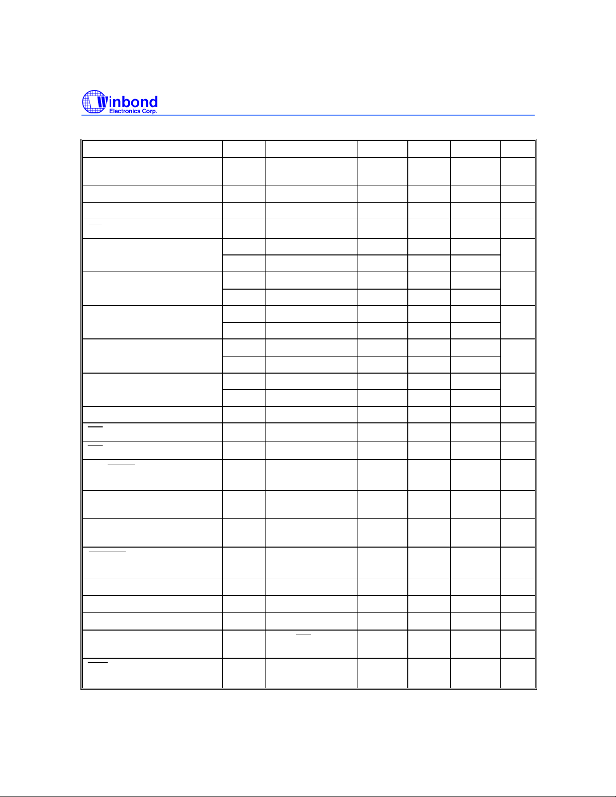
PARAMETER SYM. CONDITIONS MIN. TYP. MAX. UNIT
Operating Voltage VDD
Operating Current IOP Tone, Unloaded - 0.5 0.7
Pulse, Unloaded - 0.4 0.5
Standby Current ISB
and no key entry
Memory Retention Current IMR
VDD = 1.0V
Tone Output Voltage VTO Row group
RL = 10 KΩ
Pre-emphasis
Col/Row
VDD = 2.0 to 5.5V
- 2.0 - 5.5 V
= 0, Unloaded
= 1
- - 15
- - 0.5
130 150 170 mVrm
- 2 3 dB
µA
µA
s
Publication Release Date: May 1997
- 17 - Revision A2
Page 18
W91570DN SERIES
DP
HFI
HFI
MUTE
K MUTE
HFI
HKS
DC Characteristics, continued
PARAMETER SYM. CONDITIONS MIN. TYP. MAX. UNIT
DTMF Distortion THD RL = 10 KΩ
VDD = 2.0 to 5.5V
DTMF Output DC Level VTDC VDD = 2.0 to 5.5V 1.0 - 3.0 V
DTMF Output Sink Current ITL VTO = 0.5V 0.2 - - mA
Output Sink Current
Common Output Voltage VCH
Common Output Current ICH - -20 - -
Segment Output Voltage VSH - 4.2 4.5 4.8 V
Segment Output Current ISH - -5 - -
RMS Voltage Across a VON - 2.34 2.6 - Vrms
Segment VOFF - - 1.5 1.65
Average DC Offset Voltage VDC - - - 100 mV
High Voltage
Low Voltage
T/P
Current
H/P MUTE Output Drive
Current
H/P MUTE Output Sink
Current
Current
Keypad Input Drive Current IKD VI = 0V 4 - 80
Keypad Input Sink Current IKS VI = 2.5V 200 - 400
Keypad Resistance RK - - - 5
Control Input Pull Up/Down
Resistor
Input Pull High
Resistor
Output Sink
Output Sink
IPL VPO = 0.5V 0.5 - - mA
- 4.2 4.5 4.8 V
VCL - - 0 0.3
ICL - 20 - -
VSL - 0 0.3
ISL - 5 - -
VHFIH - 0.8 VDD - VDD V
VHFIL - - - 0.2 VDD V
ITML VTMO = 0.5V 0.5 - - mA
IHMH VHMO = 2.5V 0.5 - - mA
IHML VHMO = 0.5V 0.5 - - mA
IKML VTMO = 0.5V 0.5 - - mA
RCIP
RHK - - 500 2000
B/M,
- -30 -23 dB
100 - -
µA
µA
µA
µA
KΩ
KΩ
KΩ
AC CHARACTERISTICS
- 18 -
Page 19
W91570DN SERIES
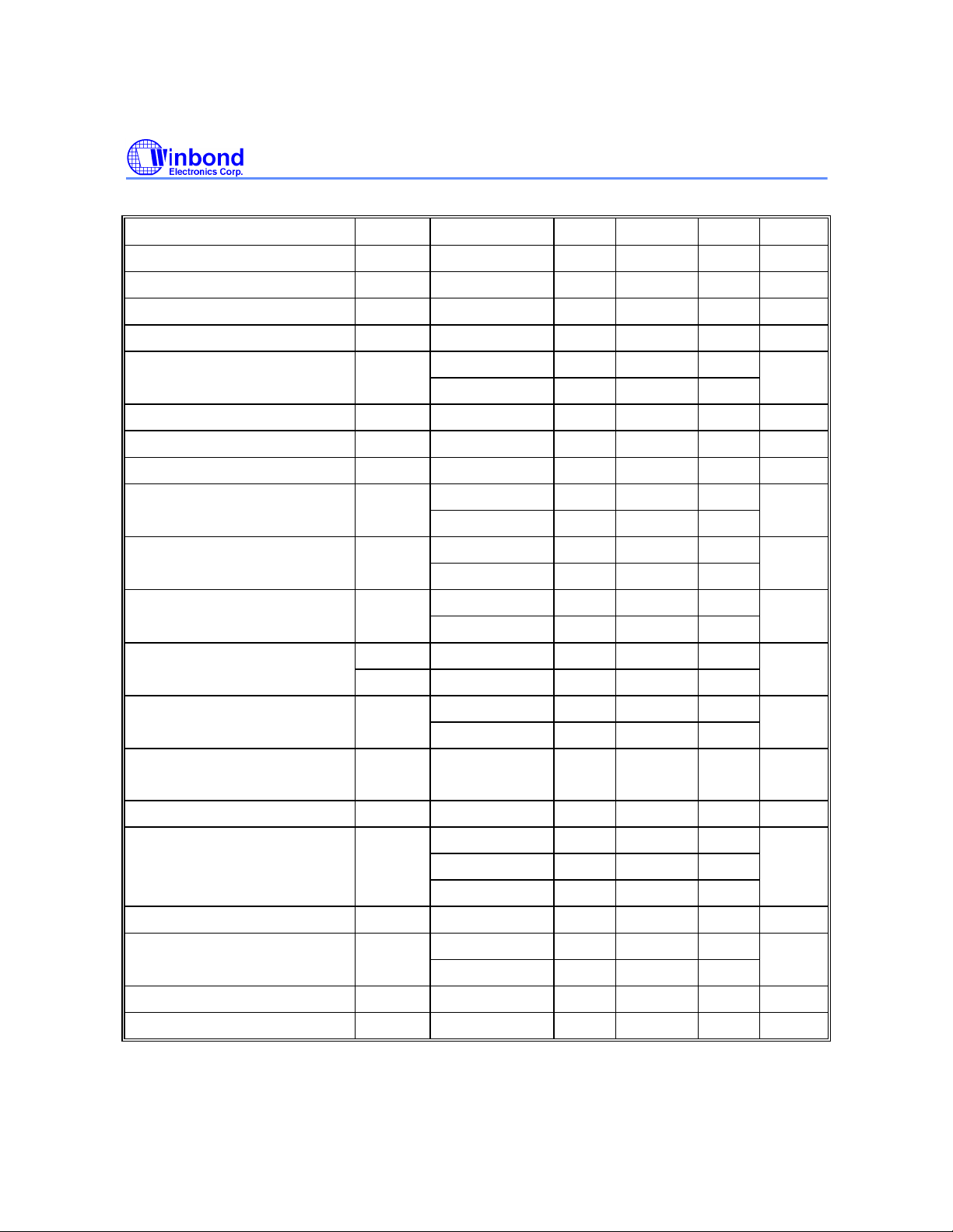
(VDD−VSS = 2.5V, FOSC. = 3.58 MHz, TA = 25° C, all outputs unloaded.)
PARAMETER SYM. CONDITIONS MIN. TYP. MAX. UNIT
Key-in Debounce TKID - - 20 - mS
Key Release Debounce TKRD - - 20 - mS
Off Hook Delay Time TOFD - - 300 - mS
First Key-in Delay Time TFKD - - 300 - mS
On Hook Debounce Time TOHD Unlock - 150 -
Lock - 20 Key Tone Frequency FKT - - 1.2 - KHz
Key Tone Duration TKTD - - 35 - mS
Key Tone Delay TKD - - 20 - mS
Pulse Mute Delay TMD B/M = VDD - 40 - mS
B/M = VSS - 33.3 -
Pre-digit-pause
10 ppS B/M = VSS - 33.3 -
Pre-digit-pause
(1)
(2)
TPDP1 B/M = VDD - 40 - mS
TPDP2 B/M = VDD - 20 - mS
20 ppS B/M = VSS - 16.7 -
Inter-digit Pause TIDP1 10 ppS - 800 - mS
(Auto Dialing) TIDP2 20 ppS - 500 Make/Break Ratio
Tone Output Duration TTD - - 87 - mS
Inter-tone Pause TITP - 87 - mS
Flash Break Time TFB F2 - 300 - mS
Flash Pause Time TFP F1, F2, F3 - 1 - S
Pause Time TP R/P1 - 3.6 -
One Key Redialing Break Time TRB - - 4 - S
One Key Redialing Pause Time TRP - - 1 - S
B/M = VDD - 40:60 - %
B/M = VSS - 33:67 -
F1 - 600 -
F3 - 100 -
R/P2 - 2.0 -
Publication Release Date: May 1997
- 19 - Revision A2
Page 20
W91570DN SERIES
SET
SET
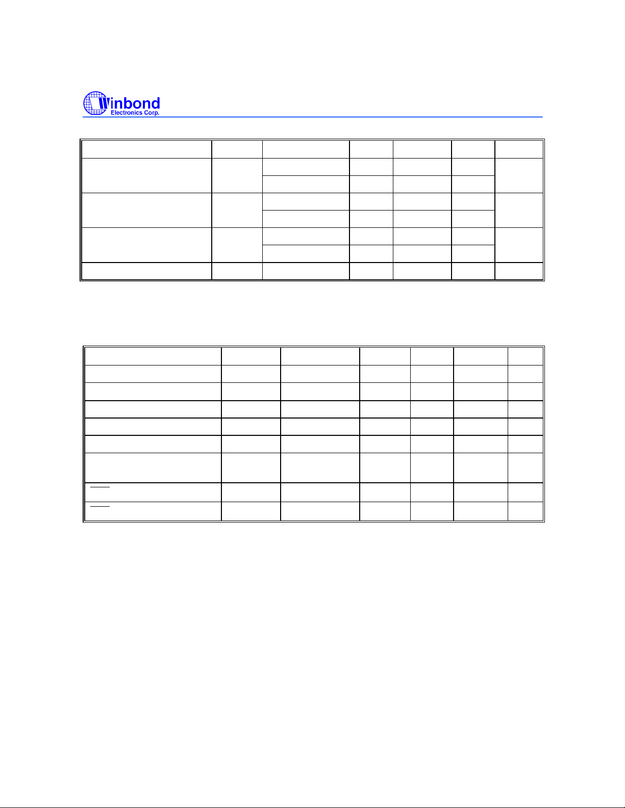
AC Characteristics, continued
PARAMETER SYMBOL CONDITIONS MIN. TYP. MAX. UNIT
Auto Redialing TARB ARD = VDD - 4 Break Time ARD = VSS - 30 -
Auto Redialing TAPR ARD = VDD - 1 Pause Time ARD = VSS - 1 -
Auto Redialing TWI ARD = VDD - 25 Waiting Interval ARD = VSS - 30 -
LCD Frame Frequency FLCD - - 32 - Hz
RTC DC CHARACTERISTICS
(VRTC = 1.5V, VSS = 0V , FOSC. = 32,768 Hz, TA = 25° C, all outputs unloaded.)
PARAMETER SYMBOL CONDITIONS MIN. TYP. MAX. UNIT
Supply Voltage VRTC
Supply Current IRTC
- 1.2 1.5 1.8 V
No Load - 2.0 4.0
µA
OSC. Starting Time TOSC - - - 3 S
OSC. Output Built-in Cap. CO
OSC. in Trimmer Cap. CTRIM
Frequency Stability
∆f/f VDD−VSS = 1.3
Cl = 12.5 pF - 25 - pF
- 5 - 35 pF
- - 1 ppM
to 1.6V
RTC Input High Voltage
RTC Input Low Voltage
Notes :
1. Crystal parameters suggested for proper operation are Rs < 100Ω, Lm = 96 mH , Cm = 0.02 pF , Cn = 5 pF , Cl = 18 pF, and
Fosc. = 3.579545 MHz ±0.02%
2. Crystal oscillator accuracy directly affects these times.
VSETH - VDD -0.3 - VDD V
VSETL - VSS - VSS +0.3 V
- 20 -
Page 21
TIMING WAVEFORMS
OSCILLATION
OSCILLATION
W91570DN SERIES
HKS
KEY IN
DP/C10
T/P MUTE
H/P MUTE
KT
DTMF
OSC.
HKS
KEY IN
DP/C10
T/P MUTE
H/P MUTE
KT
< 600mS
< 300mS
3
T
KID
T
KD
4
BM
T
IDP
T
PDP
2
M B
T
IDP
T
MD
T
IDP
2
T
KID
T
Low
OSCILLATION
OSCILLATION
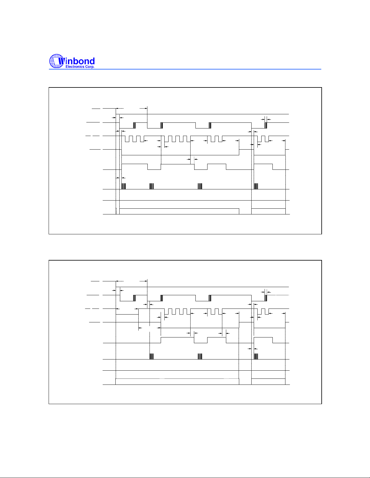
Figure 1(a). Normal Dialing Timing Diagram (Pulse Mode without Lock Function)
< 600mS
< 300mS
4
T
KID
BM
T
PDP
T
FKD
2
M B
T
IDP
T
MD
T
IDP
T
MD
2
T
KID
T
T
KD
T
3
OFD
PDP
PDP
T
T
KRD
T
KRD
T
IDP
IDP
DTMF
Low
OSC.
Figure 1(b). Normal Dialing Timing Diagram (Pulse Mode with Lock Function)
- 21 - Revision A2
Publication Release Date: May 1997
Page 22
Timing Waveforms, continued
OSCILLATION
W91570DN SERIES
HKS
KEY IN
DP/C10
T/P MUTE
H/P MUTE
KT
DTMF
OSC.
HKS
< 600mS
T
R/P
KRD
T
KID
BM
T
PDP
T
KD
M B
T
IDP
T
MD
T
IDP
T
MD
T
IDP
Low
Figure 1(c). Auto Dialing Timing Diagram (Pulse Mode without Lock Function)
< 600mS
KEY IN
DP/C10
T/P MUTE
H/P MUTE
KT
DTMF
OSC.
T
FKD
R/P
T
KID
BM
T
PDP
M B
T
IDP
T
MD
T
IDP
T
MD
300mS
T
OFD
Low
OSCILLATION
Figure 1(d). Auto Dialing Timing Diagram (Pulse Mode with Lock Function)
- 22 -
T
IDP
Page 23
Timing Waveforms, continued
OSCILLATION
OSCILLATION
W91570DN SERIES
HKS
KEY IN
DTMF
T/P MUTE
H/P MUTE
KT
DP/C10
OSC.
HKS
KEY IN
DTMF
T/P MUTE
H/P MUTE
KT
DP/C10
< 600mS
< 300mS
3
T
KID
T
TD
T
KD
4
2
T
ITP
T
ITP
Low
T
KRD
5
T
ITP
2
T
KID
High
OSCILLATION OSCILLATION
OSCILLATION
Figure 2(a). Normal Dialing Timing Diagram (Tone Mode without Lock Function)
< 600mS
< 300mS
4
T
KD
T
FKD
2
T
TD
5
T
ITP
T
ITP
Low
2
T
KID
T
3
OFD
T
KRD
T
ITP
T
KRD
T
ITP
OSC.
Figure 2(b). Normal Dialing Timing Diagram (Tone Mode with Lock Function)
Publication Release Date: May 1997
- 23 - Revision A2
Page 24
Timing Waveforms, continued
W91570DN SERIES
HKS
KEY IN
DTMF
T/P MUTE
H/P MUTE
KT
DP/C10
OSC.
HKS
KEY IN
DTMF
T/P MUTE
H/P MUTE
KT
DP/C10
OSC.
< 600mS
T
R/P
KRD
T
KID
T
TD
T
KD
Low
T
ITP
T
ITP
High
OSCILLATION
Figure 2(c). Auto Dialing Timing Diagram (Tone Mode without Lock Function)
< 600mS
T
KRD
R/P
T
KD
300mS
T
OFD
T
FKD
T
TD
OSCILLATION
Low
Low
T
ITP
T
ITP
T
OHD
T
OHD
Figure 2(d). Auto Dialing Timing Diagram (Tone Mode with Lock Function)
- 24 -
Page 25
Timing Waveforms, continued
W91570DN SERIES
HKS
KEY IN
DP/C10
T/P MUTE
H/P MUTE
KT
DTMF
OSC.
< 600mS
300mS
T
OFD
OKR
BM
T
FKD
OKR
T
KID
T
PDP
T
MD
T
IDP
Low
OSCILLATION
Figure 3. One-key Redial Timing Diagram
T
T
RB
T
RP
IDP
BM
T
PDP
HKS
HFI
HFO
T/P MUTE
H/P MUTE
DP/C10
OSC.
High
T
OSC.
OFD
T
FKD
T
OHD
OSC.
Low
OSC.
Figure 4(a). Handfree Timing Diagram (with Lock Function)
Publication Release Date: May 1997
- 25 - Revision A2
T
OHD
Page 26
Timing Waveforms, continued
HKS
HFI
HFO
W91570DN SERIES
T/P MUTE
H/P MUTE
DP/C10
HKS
KEY IN
DP/C10
T/P MUTE
H/P MUTE
DTMF
OSC.
High
Low
High
T
OHD
Figure 4(b). Handfree Timing Diagram (without Lock Function)
MER
T
KID
M
B
T
PDP
M
B
T
IDP
T
P
T
OHD
T
ITP
OSC.
OSCILLATION
Figure 5. Mercury Function Timing Diagram
- 26 -
Page 27
Timing Waveforms, continued
W91570DN SERIES
HKS
KEY IN
DP/C10
T/P MUTE
H/P MUTE
KT
DTMF
OSC.
HKS
< 600mS
2
300mS
T
OFD
T
FKD
OSCILLATION
R/P
T
KID
BM
T
PDP
T
MD
3
T
P
Low
OSCILLATION
Figure 6. Pause Function Timing Diagram (Pulse Mode)
< 600mS
T
IDP
M
B
T
PDP
T
MD
KEY IN
DP/C10
T/P MUTE
H/P MUTE
KT
DTMF
OSC.
300mS
T
OFD
T
FKD
OSCILLATION
2
*/T
T
KID
BM
T
PDP
T
IDP
3
T
P
TMD
OSCILLATION
Figure 7. Pulse to Tone Timing Diagram
- 27 - Revision A2
T
ITP
Publication Release Date: May 1997
Page 28
Timing Waveforms, continued
W91570DN SERIES
HKS
KEY IN
DP/C10
T/P MUTE
H/P MUTE
KT
DTMF
OSC.
Low
F
F
T
KID
F
T
FB
T
KID
3
T
KID
T
FP
OSCILLATION
Figure 8. First Priority Flash Timing Diagram
T
ITP
HKS
KEY IN
DP/C10
T/P MUTE
H/P MUTE
KMUTE
OSC.
Timing Waveforms, continued
Low
MUTE
4
M
B
2
T
KID
T
IDP
T
PDP
2
T
KID
M
B
T
IDP
MUTE
T
KID
M
B
T
IDP
OSCILLATION
Figure 9. Mute Timing Diagram
- 28 -
Page 29
W91570DN SERIES
HKS
HFI
HOLD KEY
HFO
T/P MUTE
H/P MUTE
CHIP ENBLE
OFF HOOK
Figure 10(a). Hold and Handfree Timing Diagram
Note: The HOLD KEY cannot be enabled when the chip is disabled.
HKS
HFI
ON HOOK
High
Low
OFF HOOK
HOLD KEY
HFO
T/P MUTE
H/P MUTE
CHIP ENBLE
High
Figure 10(b). Hold and Handfree Timing Diagram
Note: The HFI and HOLD KEY inputs will toggle the HFO signal; as soon as either HFI or HOLD KEY is activated, the HFO
signal will go high and previous activate inputs will be ignored.
Publication Release Date: May 1997
- 29 - Revision A2
Page 30
Timing Waveforms, continued
W91570DN SERIES
HKS
ON HOOK
HFI
HOLD KEY
HFO
T/P MUTE
High
H/P MUTE
CHIP ENBLE
Figure 10(c). Hold and Handfree Timing Diagram
Note: Changing the state of the HKS signal from high to low will initialize the HFO and HPM MUTE signals.
KEY IN
KT
DP/C10
OKR
KD
T
AUTO
ARP
REDIALING
T
ARB
INTERVAL
WAITINGT
INTERVAL
REPEAT TILL
N-1 TIMES
ARB
T
AUTO
T
ARP
REDIALING
INTERVAL
WAITING
INTERVAL
Notes:
OSC.
OSCILLATION
Figure 11(a). Auto Redialing Timing Diagram
1. The auto redial function is enabled in off-hook or handfree state.
2. If OKR is the first key-in after off-hook or handfree then the first TARB and TARP will be ignored.
- 30 -
Page 31
Timing Waveforms, continued
KEY IN
KT
DP/C10
OKR
W91570DN SERIES
Any
Keypad
KD
T
AUTO
T
ARP
REDIALING
T
ARB
INTERVAL
WAITING
INTERVAL
ARB
T
AUTO
T
ARP
REDIALING
INTERVAL
WAITING
INTERVAL
KD
T
OSC.
OSCILLATION
Figure 11(b). Auto Redialing Timing Diagram
Publication Release Date: May 1997
- 31 - Revision A2
Page 32
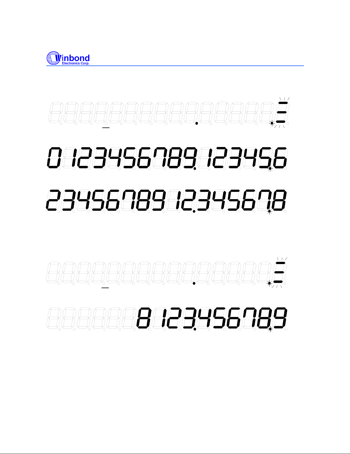
LCD DISPLAY FORMAT
A. Normal Dialing
W91570DN SERIES
Off hook or press the "HFI" switch
(Here tone mode was selected).
Dial" 0123456789123456"
and "78"
B. Redialing, Save Dialing, One Touch Dialing
Off hook or press the "HFI" switch
(Here tone mode was selected).
Blinking
Blinking
Press the "R/P", "OKR", "SAVE" or "Mn" key
(Redial or SAVE or Mn = "8123456789")
- 32 -
Page 33
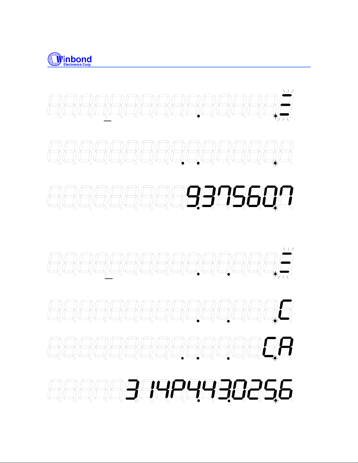
C. Abbreviated Auto Dialing
W91570DN SERIES
Off hook or press the "HFI" switch
(Here tone mode was selected).
Press the "A1" key in chip enable condition
(L5 = "9375607", here L5 is the fifth memory)
Press the "5" key
D. Memory Check
a.
Off-hook or press the "HFI" switch
(L6 = "314P4430256", and here handfree and tone mode were selected)
Blinking
Blinking
Press the "CHK" key
Press the "A1" key
(The auto(A) is shown on check and store mode)
Press the "6" key
Publication Release Date: May 1997
- 33 - Revision A2
Page 34
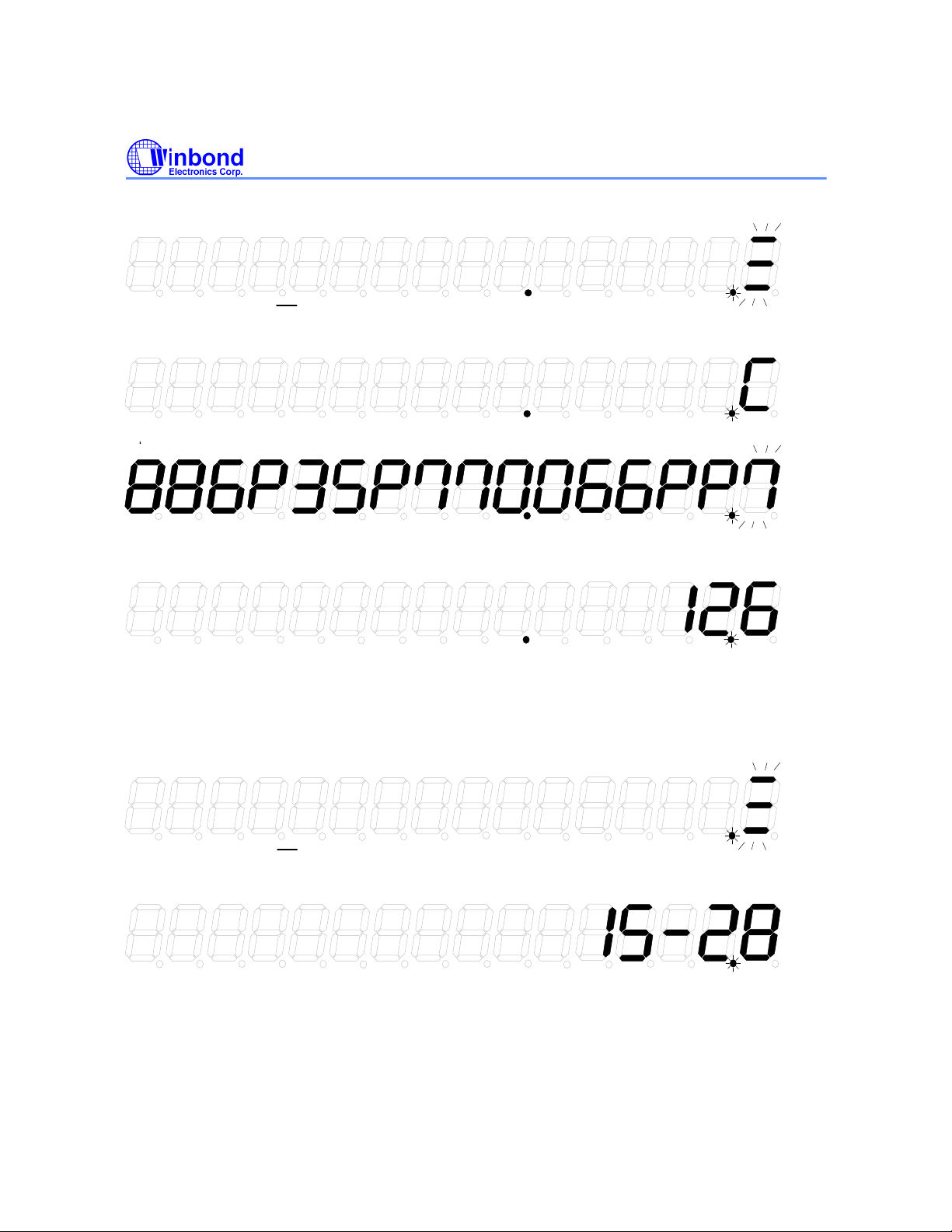
b.
W91570DN SERIES
Off-hook or press the "HFI" switch
(M1= "886P35P770066PP7126", and here pulse mode was selected)
Press the "CHK"
Press the "M1" key
(Display 1 to 16 digits)
Press "any key"
(Display 17 to 19 digits)
E. Timer Function
a.
Blinking
Blinking
Off-hook or press the "HFI" switch
(here pulse mode was selected)
Press the "TIM" key
(Display last calling time)
Blinking
- 34 -
Page 35
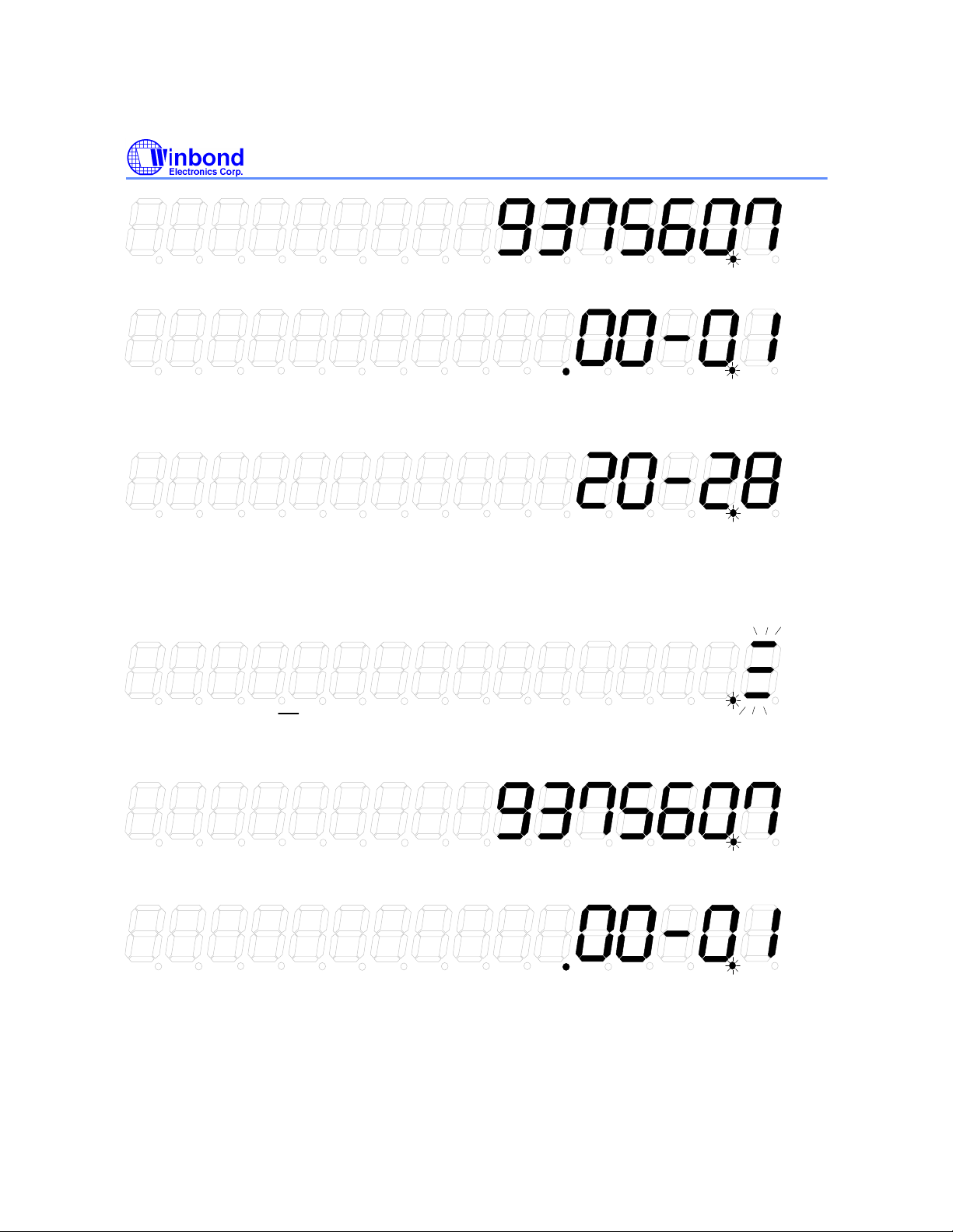
W91570DN SERIES
Dial "9375607"
If "9375607" is dialed completed, the system will start timer after 6 seconds
(Timer will start counting up)
Press the "TIM"
(Timer will stop)
b.
Off-hook or press the "HFI" switch
(here pulse mode was selected)
Dial "9375607"
If "9375607" is dialed completed
press the "TIM" key
(Timer will start counting up)
Blinking
Publication Release Date: May 1997
- 35 - Revision A2
Page 36
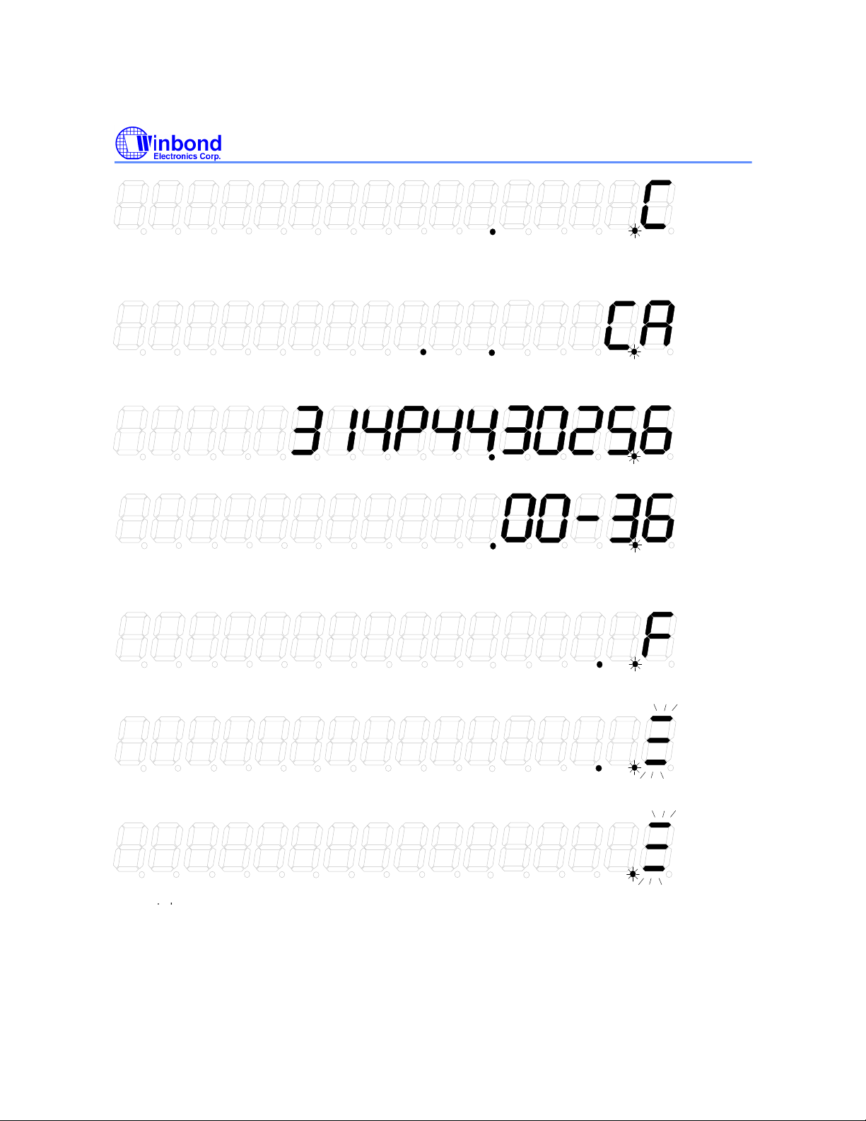
Press the "CHK" key
(L6 = "314P4430256")
Press the "A1" key
Press the "6" key
W91570DN SERIES
The system will go back to timer mode after 6 seconds
(Timer count up continuously)
Press the "F1", "F2" or "F3" key
(The timer will stop and LCD will display a flash mark and flash pattern)
After flash break is executed
After flash pause is
Blinking
Blinking
- 36 -
Page 37
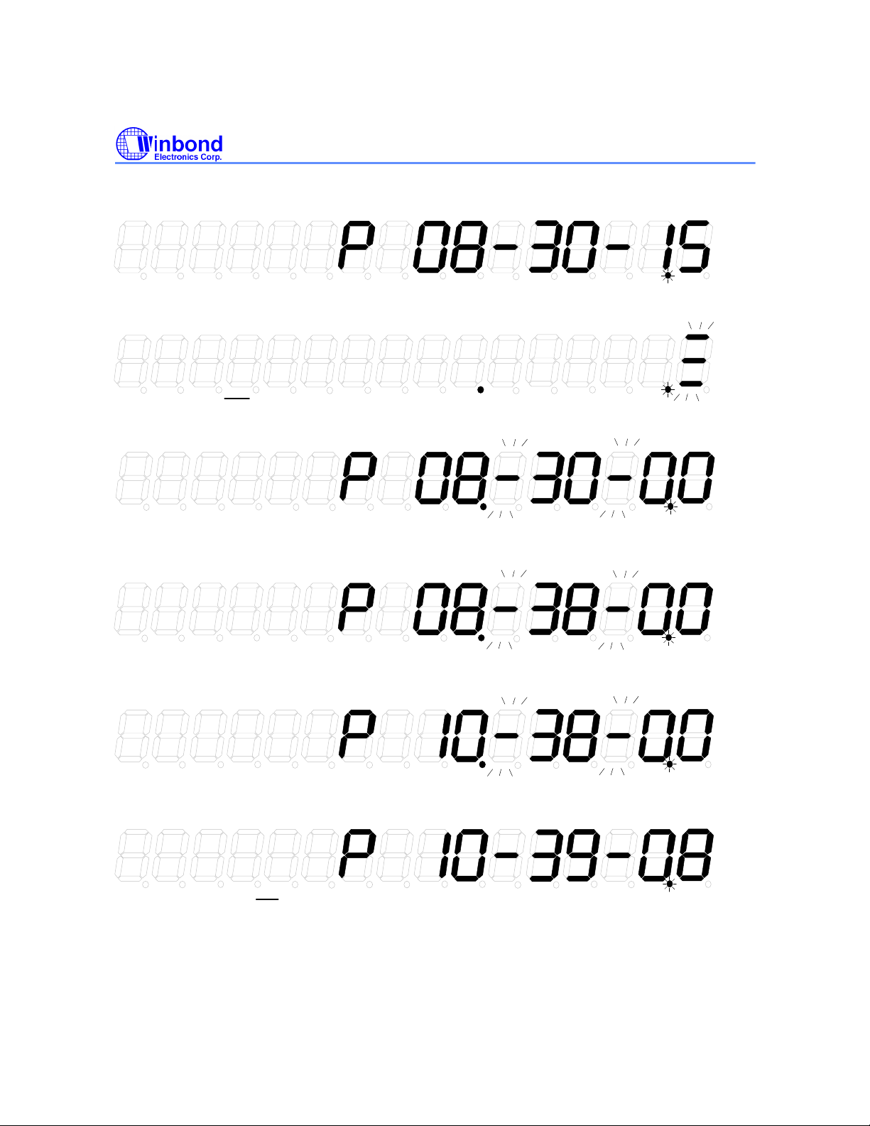
F. RTC Setting Function
On-hook
(Display real time)
W91570DN SERIES
Off-hook, before SET pin was switched ON
(Here tone mode was selected)
RTC
Entering "Setting Mode"
Adjusting "Hour"
(Hour counts forward as long as pressing)
Adjusting "Minute"
(Minute counts forward as long as pressing)
Blinking
Blinking
On-hook or switching SET pin OFF
(Here on-hook was selected)
RTC
Publication Release Date: May 1997
- 37 - Revision A2
Page 38
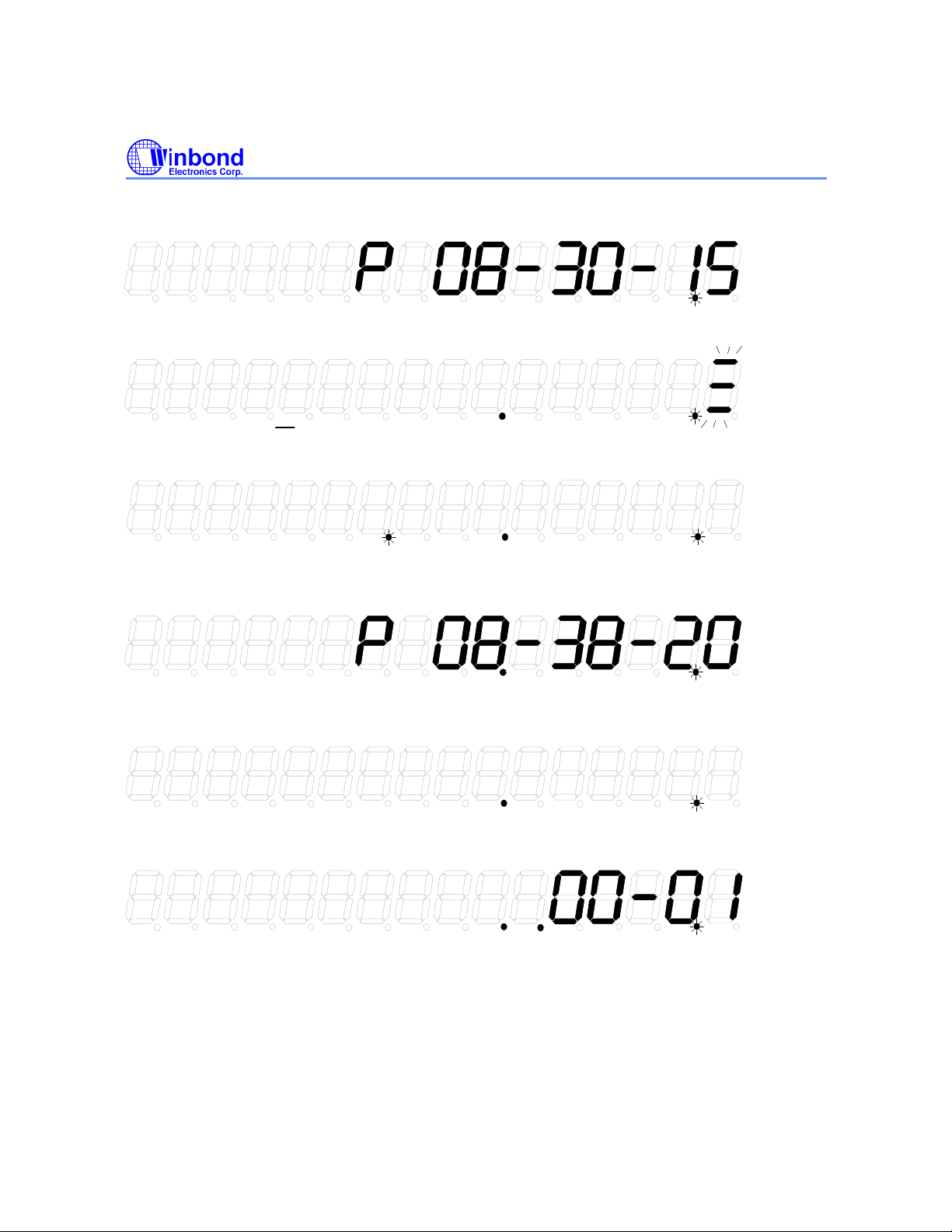
G. RTC Display Function
On-hook
(Display real time)
W91570DN SERIES
Off-hook or press the "HFI" switch
(Here off-hook and tone mode was selected)
Press the "MER" key
(MER = "035PP770066")
Press the "RTC" key when "MER" dialing
is completed within 6 seconds.
Press the "RTC" key again
Blinking
Blinking
If the "MER" is dialed completed for 6 seconds
- 38 -
Page 39
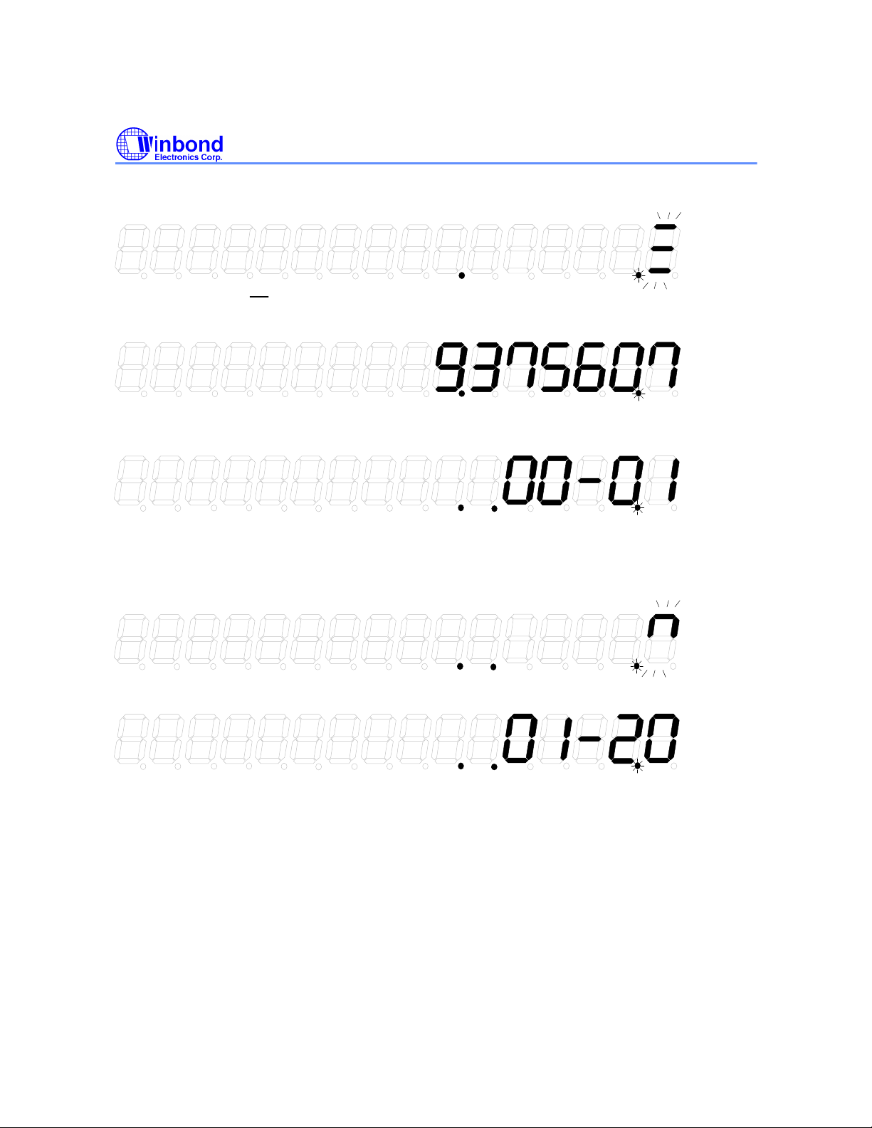
H. Mute Function
W91570DN SERIES
Off-hook or press the "HFI" switch
Dial "9375607"
If "9375607" is dialed completed
Press the "TIM" key
(Timer will start counting up)
Press the "MUTE"
Blinking
Blinking
Press the "MUTE" key again
Publication Release Date: May 1997
- 39 - Revision A2
Page 40
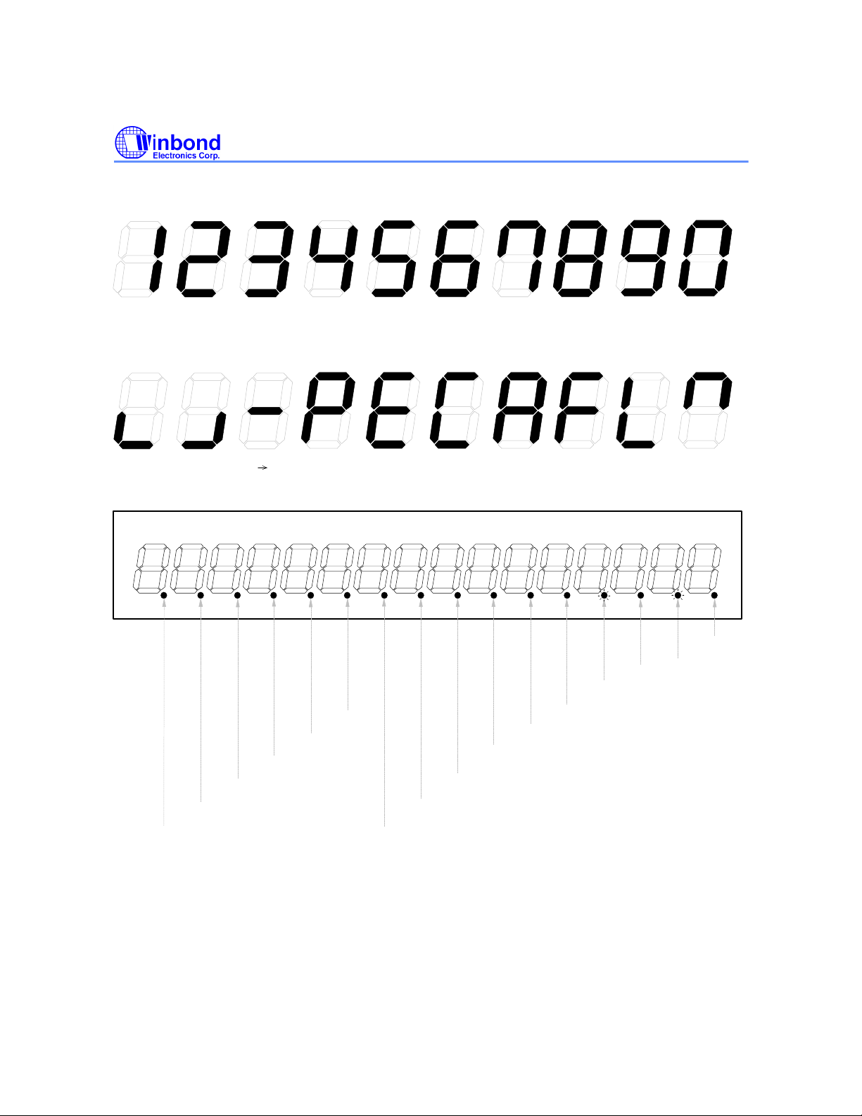
LCD PATTERN FOR DATA
Icon
W91570DN SERIES
1
2 3 4
* # P T P
Icon12
Icon13
Icon14
Icon15
Icon16
ARD/
Icon11
5 6 7 8 9
E
Mercury/
Iocn10
CHECK A
Page 1 (for A1)/
Icon8
Page 2 (for A2)/
Icon9
Tone/
Icon7
Timer/
Icon6
F
Handfree/
Icon5
Hold/
Icon4
LOCK
Flash/
Icon3
MUTE
Inuse/
0
Pause/
Icon1
Notes:
1. The icon1 to icon 10 are controlled by function operation.
2. The icon 12 to icon16 can be toggled on/off individually, irrespective of keypad function.
3. The off-hook (or hand free) state of icon12 is on, the other icons are off.
4. The icon2 always blinked after power on.
- 40 -
Page 41
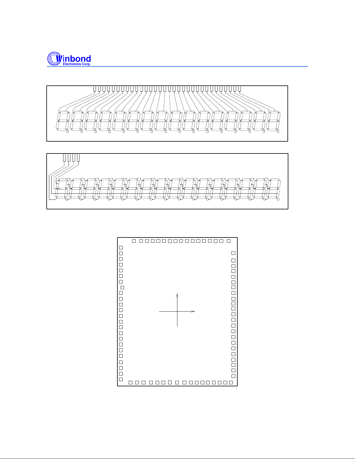
LCD PANEL PATTERN
(COM)
59
2930313
2
C
C
C
C
O
O
O
O
M
M
M
M
123
4
8
W91570DN SERIES
1
7
12345678910111213141516181920212223242526272
(SEG)
BONDING PAD DIAGRAM
2
3
4
5
6
7
8
9
10
11
12
13
14
15
16
17
18
19
20
21
22
23
24
25
Notes:
1. The substrate must be connected to VSS
1
81 80 79 78 777675 74 73 72 71 70
Y
(0,0)
26 27 28 29 30 313233 34 35 36 37 38 39 40
69 68
X
66
67
65
64
63
62
61
60
58
57
56
55
54
53
52
51
50
49
48
47
46
45
44
43
41
42
Publication Release Date: May 1997
- 41 - Revision A2
Page 42

W91570DN SERIES
2. The chip size is 3450 × 4280 µm
2
- 42 -
Page 43
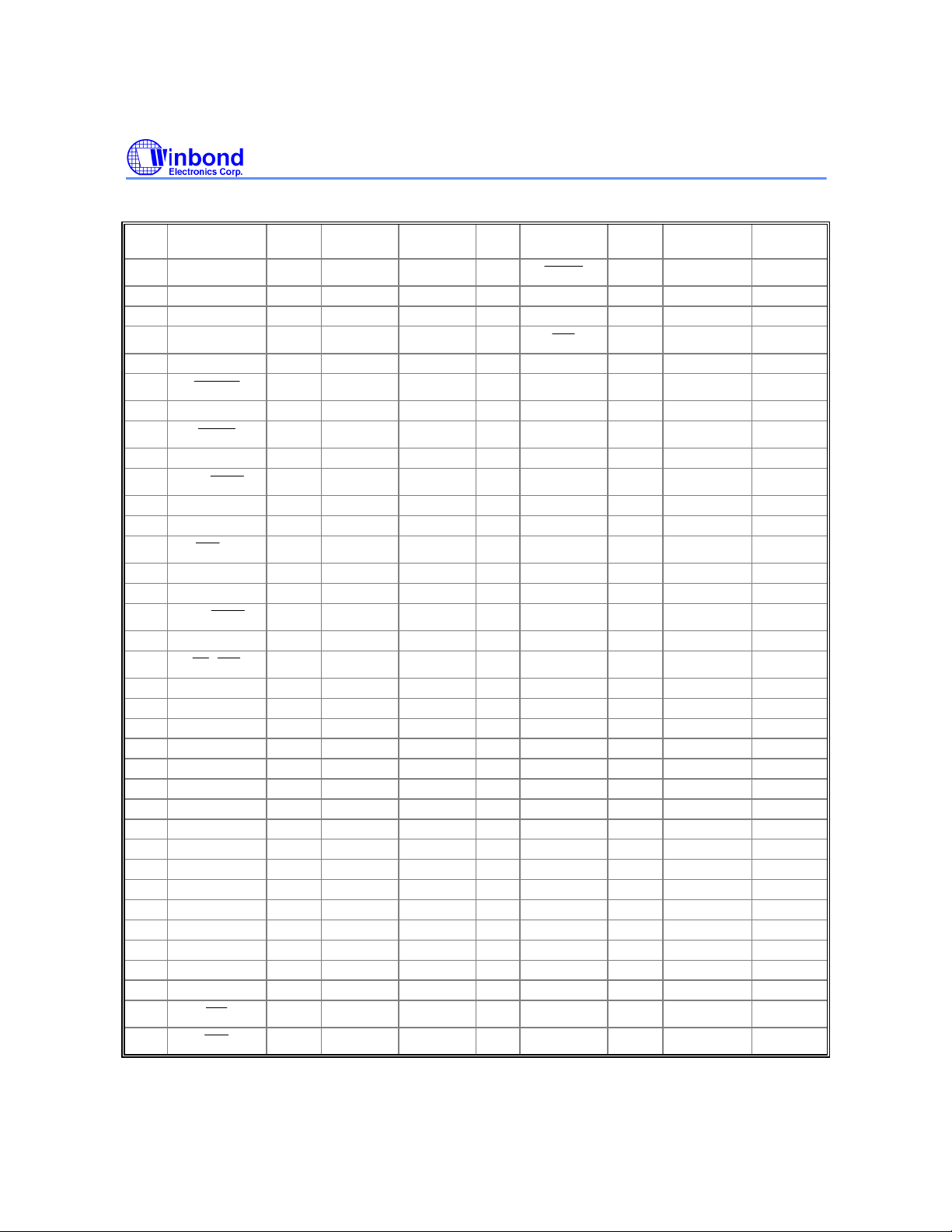
W91570DN SERIES
Bonding Pad List
PAD
NO.
1 SEG29<15> 1 -1205.80 1988.70 42
2 SEG30<15> 2 -1581.90 1871.70 43 APSET 42 1589.40 -1805.40
3 SEG31<16> 3 -1581.90 1716.70 44 XT2 43 1589.40 -1638.20
4 SEG32<16> 4 -1581.90 1561.70 45
5 TEST 5 -1581.90 1389.40 46 VLCD 45 1589.40 -1333.60
6
7 KT 7 -1581.90 1073.20 48 CN 47 1589.40 -996.00
8
9 VDD 9 -1546.90 749.00 50 COM<1> 49 1589.40 -668.90
10
11 B/M 11 -1581.90 421.10 52 COM<3> 51 1589.40 -358.90
12 DTMF 12 -1581.90 248.00 53 COM<4> 52 1589.40 -203.90
13
15 VSS 14 -1581.90 -241.00 55 SEG2<1> 54 1589.40 106.10
16 H/P MUTE 15 -1581.90 -391.00 56 SEG3<2> 55 1589.40 261.10
17
18 HFO 17 -1581.90 -707.20 58 SEG5<3> 57 1589.40 571.10
19
20 MODE 19 -1581.90 -1023.40 60 SEG7<4> 59 1589.40 881.10
21 COL1 20 -1581.90 -1194.10 61 SEG8<4> 60 1589.40 1036.10
22 COL2 21 -1581.90 -1377.10 62 SEG9<5> 61 1589.40 1191.20
23 COL3 22 -1581.90 -1560.30 63 SEG10<5> 62 1589.40 1346.20
24 COL4 23 -1581.90 -1743.30 64 SEG11<6> 63 1589.40 1501.20
25 COL5 24 -1581.90 -1926.50 65 SEG12<6> 64 1589.40 1720.60
26 COL6 25 -1196.70 -2009.80 66 SEG13<7> 65 1407.40 1987.70
27 COL7 26 -1013.70 -2009.80 67 SEG14<7> 66 1158.00 1987.70
28 COL8 27 -830.50 -2009.80 68 SEG15<8> 67 1003.00 1987.70
29 COL9 28 -647.50 -2009.80 69 SEG16<8> 68 848.00 1987.70
30 ROW1 29 -464.30 -2009.80 70 SEG17<9> 69 693.00 1987.70
31 ROW2 30 -281.30 -2009.80 71 SEG18<9> 70 538.00 1987.70
32 ROW3 31 -98.10 -2009.80 72 SEG19<10> 71 383.00 1987.70
33 ROW4 32 84.90 -2009.80 73 SEG20<10> 72 228.00 1987.70
34 ROW5 33 268.10 -2009.80 74 SEG21<11> 73 72.90 1987.70
35 XT1 34 435.60 -2009.80 75 SEG22<11> 74 -82.10 1987.70
36
37
PAD
NAME
K MUTE
TEST1
NC/LOCK
SET RTC
T/P MUTE
DP / C10
XT1
HKS
PIN
NAME
6 -1581.90 1231.40 47 VRTC2 46 1589.40 -1179.00
8 -1581.90 915.20 49 CP 48 1589.40 -844.00
10 -1581.90 579.10 51 COM<2> 50 1589.40 -513.90
13 -1581.90 67.00 54 SEG1<1> 53 1589.40 -48.90
16 -1581.90 -549.20 57 SEG4<2> 56 1589.40 416.10
18 -1581.90 -865.40 59 SEG6<3> 58 1589.40 726.10
35 585.60 -2009.80 76 SEG23<12> 75 -237.10 1987.70
36 735.60 -2009.80 77 SEG24<12> 76 -392.10 1987.70
X Y PAD
NO.
PAD
NAME
TESTL
XT2
PIN
NAME
41 1514.90 -2009.80
44 1589.40 -1488.20
X Y
Publication Release Date: May 1997
- 43 - Revision A2
Page 44
W91570DN SERIES
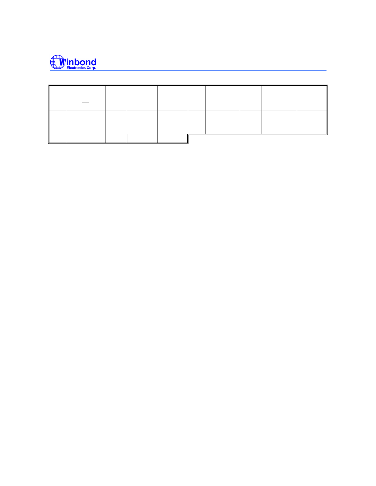
Bonding Pad List, continued
PAD
NO.
38
39 VRTC1 38 1040.70 -2009.80 79 SEG26<13> 78 -702.10 1987.70
40 TEST2 39 1198.80 -2009.80 80 SEG27<14> 79 -857.10 1987.70
41 ARD 40 1356.80 -2009.80 81 SEG28<14> 80 -1012.10 1987.70
14 DISP -1581.90 -91.00
Note: Pad 14 is for 12-digit LCD display bonding only.
PAD
NAME
HFI
PIN
NAME
37 885.60 -2009.80 78 SEG25<13> 77 -547.10 1987.70
X Y PAD
NO.
PAD
NAME
PIN
NAME
X Y
- 44 -
Page 45

W91570DN SERIES
Headquarters
No. 4, Creation Rd. III,
Science-Based Industrial Park,
Hsinchu, Taiwan
TEL: 886-3-5770066
FAX: 886-3-5792697
http://www.winbond.com.tw/
Voice & Fax-on-demand: 886-2-7197006
Winbond Electronics (H.K.) Ltd.
Rm. 803, World Trade Square, Tower II,
123 Hoi Bun Rd., Kwun Tong,
Kowloon, Hong Kong
TEL: 852-27513100
FAX: 852-27552064
Taipei Office
11F, No. 115, Sec. 3, Min-Sheng East Rd.,
Taipei, Taiwan
TEL: 886-2-7190505
FAX: 886-2-7197502
Note: All data and specifications are subject to change without notice.
Winbond Electronics North America Corp.
Winbond Memory Lab.
Winbond Microelectronics Corp.
Winbond Systems Lab.
2730 Orchard Parkway, San Jose,
CA 95134, U.S.A.
TEL: 1-408-9436666
FAX: 1-408-9436668
Publication Release Date: May 1997
- 45 - Revision A2
 Loading...