

Page 1
W9145 SERIES
15-MEMORY TONE/PULSE DIALER WITH LOCK
AND HANDFREE FUNCTIONS
GENERAL DESCRIPTION
The W9145 series are Si-gate CMOS ICs that provide the necessary signals for either pulse or tone
dialing. The W9145 series feature a key tone function, handfree dialing, a lock function, thirteen 16digit automatic dialing memories, and two by 32-digit for redial and save memory.
FEATURES
• DTMF/Pulse switchable dialer
• Two by 32 digits for redial and save memory
• Three by 16 digits for one-touch direct repertory
• Ten by 16 digits for two-touch indirect repertory
• Unlimited dialing length (redial inhibited if dialing length exceeds 32 digits in normal dialing)
• Auto Pause Access for PBX and toll service operations (3.1 seconds per pause)
• Easy operation with redial, store, auto and pause keypads
• Key tone output for recognition of valid keypad entry
• Call disconnect (CD) key for line break operation
• Mute key for speech mute
• Flash time: 98 mS, 305 mS or 600 mS
• Minimum tone output duration: 93 mS
• Minimum intertone pause: 93 mS
• 0 or 9 dialing inhibition pin for PABX system or long distance dialing lock out
• Automatic switching from pulse mode to tone mode by */T key operation
• Break/make ratio pin selectable
• Uses Form A keyboard or standard 5 × 5 matrix keyboard
• Uses inexpensive 3.579545 MHz television color-burst crystal
• Internally generated power-on reset
• Packaged in 22/24-pin DIP
• The different dialers in the W9145 series are shown in the following table:
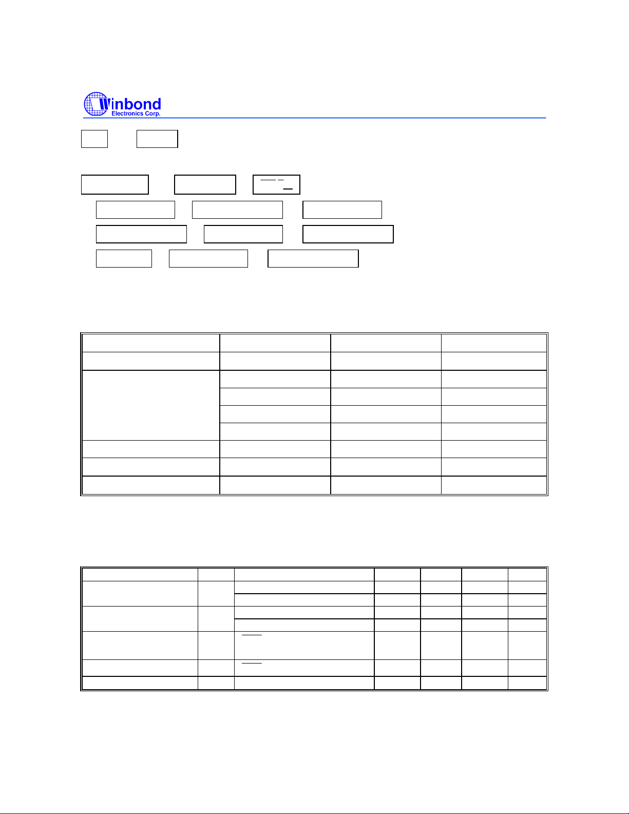
TYPE NO. PULSE (ppS) FLASH B/M HANDFREE LOCK
W9145 10 98/305/600 Pin No No
W9145A 10 98/305/600 Pin Yes No
W9145L 10 98/305/600 Pin No Yes
W9145AL 10 98/305/600 Pin Yes Yes
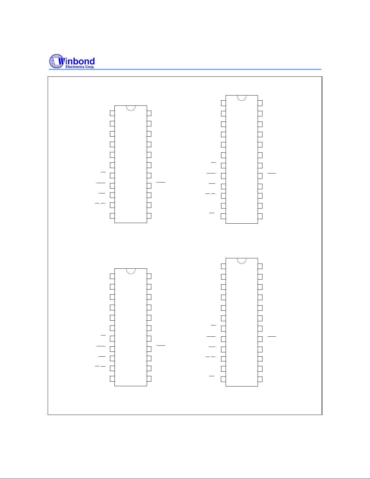
PIN CONFIGURATIONS
Publication Release Date: August 1996
- 1 - Revision A4
Page 2
W9145 SERIES
X MUTE
X MUTE
C1
C2
C3
C4
V
SS
XT
XT
T/P MUTE
HKS
DP/C5
DTMF
C1
C2
C3
C4
V
SS
XT
XT
T/P MUTE
HKS
DP/C5
DTMF
1
2
3
4
5
6
7
8
9
10 13
11
W9145
1
2
3
4
5
6
7
8
9
10 13
11
SS
XT
XT
1
2
3
4
5
6
7
8
9
10
11 14
12
C1
22
R5
R4
21
20
R3
19
R2
18
R1
V
17
16
15
14
12
DD
B/M
TEST
MODE
X MUTE
KT
C2
C3
C4
V
T/P MUTE
HKS
DP/C5
DTMF
HFI
24
R5
23
R4
R3
22
21
R2
20
R1
19
V
DD
18
B/M
17
TEST
MODE
16
15
KT
13
HFO
W9145A
SS
XT
XT
1
2
3
4
5
6
7
8
9
10
11 14
12
C1
22
R5
R4
21
20
R3
19
R2
18
R1
V
17
16
15
14
12
DD
B/M
LOCK
MODE
X MUTE
KT
C2
C3
C4
V
T/P MUTE
HKS
DP/C5
DTMF
HFI
24
R5
23
R4
R3
22
21
R2
20
R1
19
V
DD
B/M
18
17
LOCK
MODE
16
15
KT
13
HFO
PIN DESCRIPTION
W9145L
W9145AL
- 2 -
Page 3
W9145 SERIES
XT
MUTE
MUTE
HKS
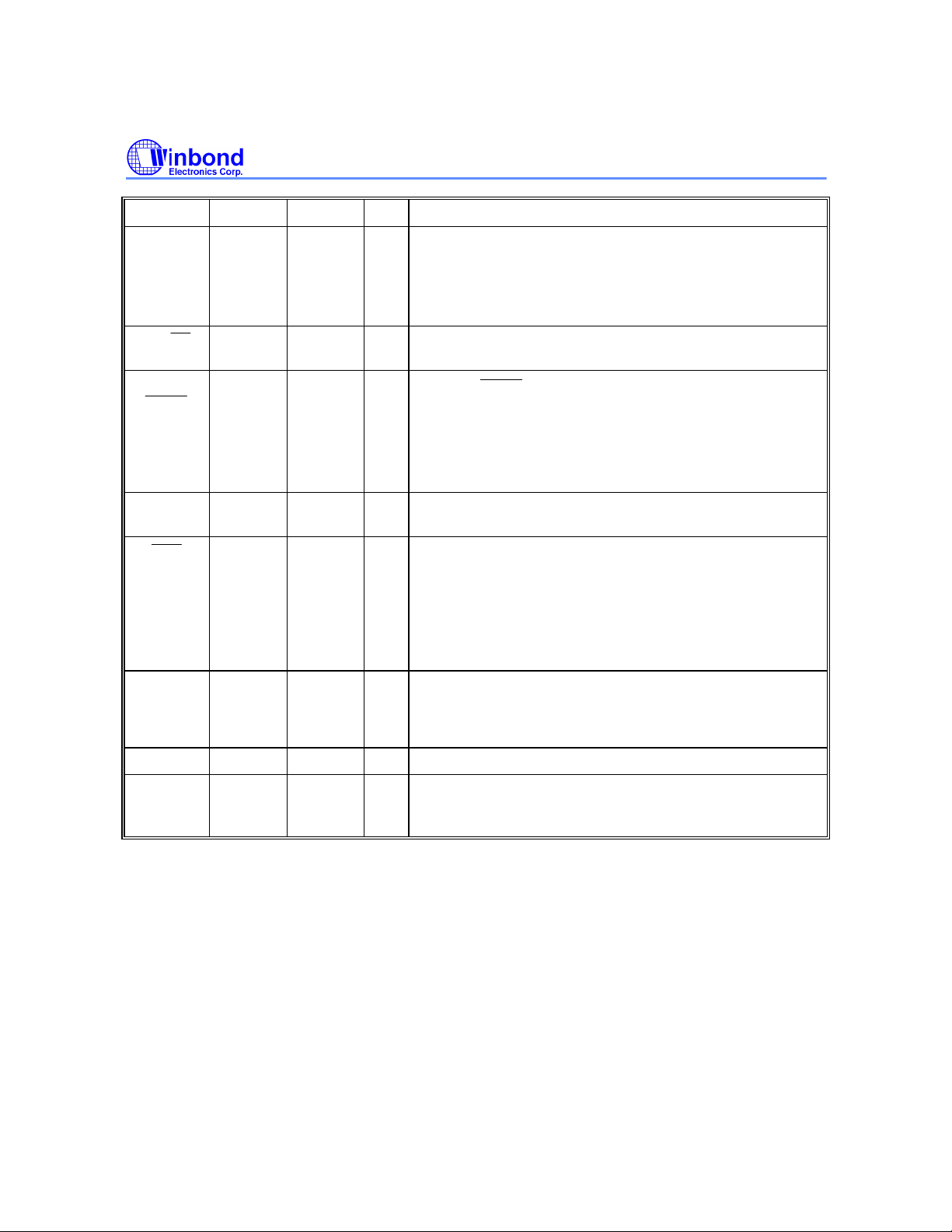
SYMBOL 22-PIN 24-PIN I/O FUNCTION
ColumnRow
Inputs
XT,
T/P
MODE 14 16 I Pull to VSS to enable tone mode. Pull to VDD to enable
B/M 16 16 I B/M = 1: Break/Make ratio is 60:40.
1−4
&
18−22
6, 7 6, 7 I, O A built-in inverter provides oscillation by means of an
8 8 O
9 9 I Hook switch input. When pulled to high, chip is in on-hook
1−4
&
20−24
I Keyboard inputs may be connected to either a standard
keyboard, an inexpensive signal contact (Form A)
keyboard, or electronic input from a µC. A valid key entry
is defined by a single row being connected to a single
column.
inexpensive 3.579545 MHz crystal or ceramic resonator.
The T/P
pulls to VDD in the absence of keypad input and pulls to
VSS when an address keypad entry is sensed (excluding
the * and # keypads in pulse mode). When any keypad in
row 5 and column 5 is pushed, the mute out remains at
high level.
pulse mode (10 ppS).
state (no operation). When pulled to low, chip is in offhook state (enabled for normal operation). This pin is
pulled to VDD by internal resistor.
Note: This pin operates in conjunction with the handfree
control pins; for further information see description of
handfree control pins below.
B/M = 0: Break/Make ratio is 67:33.
This pin has no function in tone mode.
is a conventional CMOS inverter that
VDD, VSS 17, 5 19, 5 I Power input pins.
X MUTE 13 15 O The X MUTE is a conventional CMOS inverter that in tone
mode is active while a DTMF signal is being transmitted.
In pulse mode, this output remains low at all times.
Publication Release Date: August 1996
- 3 - Revision A4
Page 4
Pin Description, continued
HFI
HFI
HFI
LOCK
TEST
TEST
DP/C5
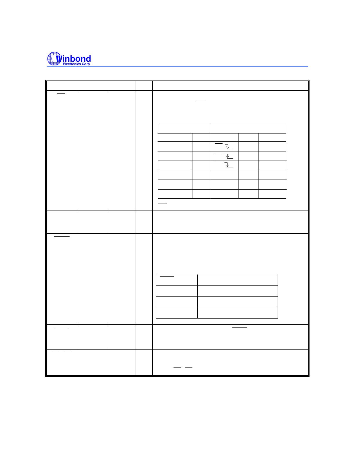
SYMBOL 22-PIN 24-PIN I/O FUNCTION
,
HFO
- 12, 13 I, O Handfree control pins.
A low pulse on
toggles on the handfree control state.
Status of the handfree control state is indicated in the
following table:
W9145 SERIES
CURRENT STATE
HOOK SW.
On Hook
Off Hook
On Hook
Off Hook
Off Hook
pin is pulled to VDD by internal resistor.
HFO
Low
High
High
Low
High
INPUT
HFI
HFI
HFI
-
Off Hook
On Hook
On Hook
NEXT STATE
HFO
High
Low
Low
Low
Low
High
DIALING
Yes
No
Yes
Yes
No
Yes
KT 12 14 O Key tone signal output. A 1.2 KHz key tone will be
generated when any key is depressed in pulse mode or
when function keys are depressed in tone mode.
15
(W9145L
only)
17
(W9145AL
only)
The function of this terminal is to prevent "0" dialing in
I
and "9" dialing under PABX system long distance call
control. When the first key input after reset is 0 or 9, all
key inputs, including the 0 or 9 key, become invalid and
the chip generates no output. The telephone is
reinitialized by a reset.
LOCK PIN
V
DD
Floating
FUNCTION
Normal dialing mode
"0," "9" dialing inhibited
"0" dialing inhibited
15
(W9145
only)
17
(W9145A
only)
V
SS
I
During normal operation, the
VDD, thereby inhibiting the single tone and setting the
pulse rate to 10 ppS.
10 10 O This pin is a CMOS inverter output.
The timing diagram is shown in Figure 1. Flash key will
cause DP/C5 to go active in either pulse or tone mode.
- 4 -
pin should be tied to
Page 5
W9145 SERIES
Pin Description, continued
SYMBOL 22-PIN 24-PIN I/O FUNCTION
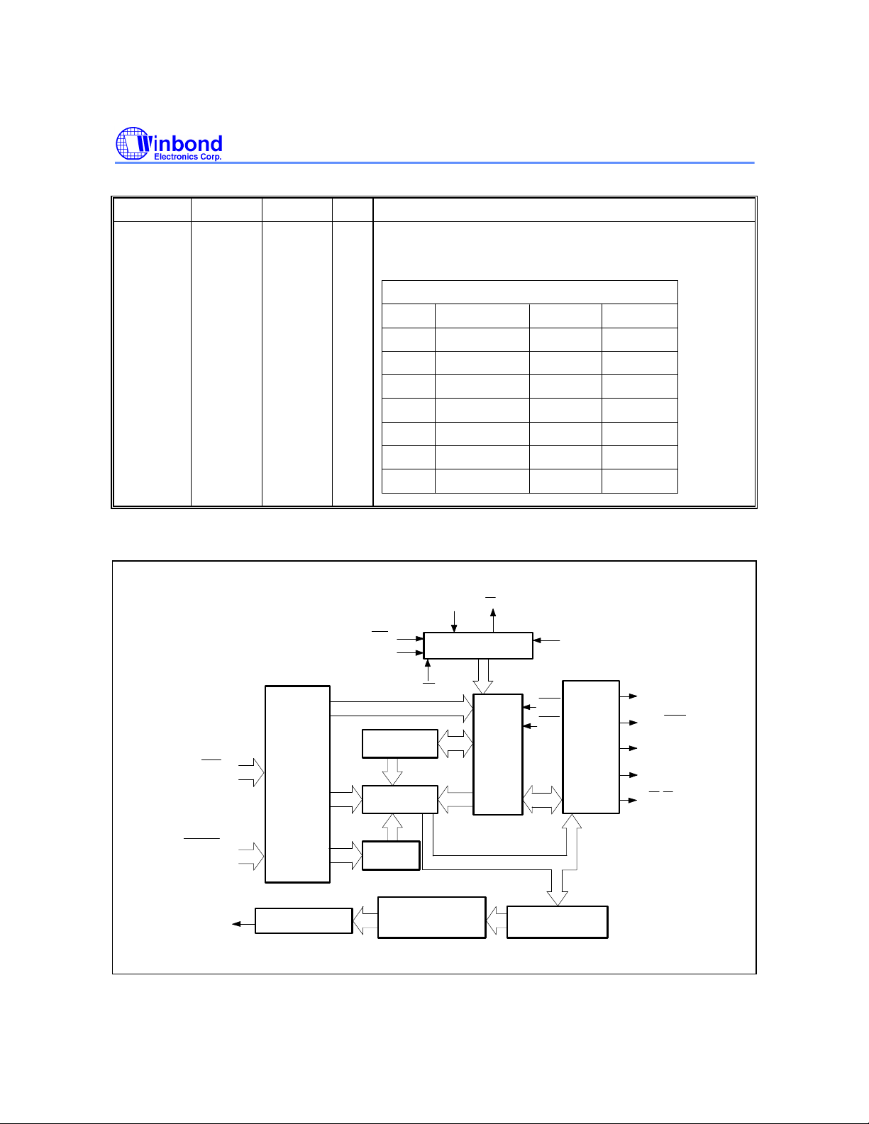
DTMF 11 11 O In pulse mode, remains in low state at all times. In tone
mode, will output a dual or single tone. Detailed timing
diagram for tone mode is shown in Figure 2(a, b).
OUTPUT FREQUENCY (Hz)
R1
R2
R3
R4
C1
C2
C3
Specified
697
770
852
941
1209
1336
1477
Actual
699
766
848
948
1216
1332
1472
Error %
+0.28
-0.52
-0.47
+0.74
+0.57
-0.30
-0.34
BLOCK DIAGRAM
ROW
(R1 to R5)
COLUMN
(C1 to C4)
DTMF
KEYBOARD
INTERFACE
D/A CONVERTER
HKS
MODE
READ/WRITE
COUNTER
RAM
LOCATION
LATCH
ROW & COLUMN
PROGRAMMABLE
COUNTER
HFI
XT XT
SYSTEM CLOCK
GENERATOR
CONTROL
LOGIC
LOCK
TEST
DATA LATCH
& DECODER
B/M
PULSE
CONTROL
LOGIC
X MUTE
T/P MUTE
KT
HFO
DP/C5
Publication Release Date: August 1996
- 5 - Revision A4
Page 6
FUNCTIONAL DESCRIPTION
DP/C5
HFI
¡õ
HFI
¡õ
HFI
¡õ
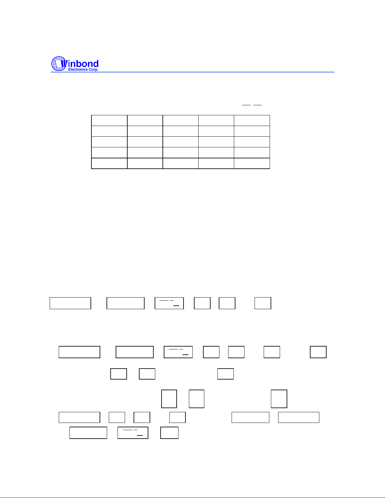
Keyboard Operation
C1 C2 C3 C4
1 2 3 M1 MUTE R1
4 5 6 M2 CD R2
7 8 9 M3 F1 R3
*/T 0 # SAVE F2 R4
RD S A P F3 R5
• MUTE: Mute key
• CD: Call Disconnect
• */T: * & P→T key
• RD: One-key Redial
• S: Store
• A: Auto dialing
• P: Pause
• M1 to M3: Memory 1 to 3
• SAVE: Save Memory
• F1, F2, F3: 98/305/600 mS
W9145 SERIES
Normal Dialing
OFF HOOK (or ON HOOK &
1. D1, D2, ..., Dn will be dialed out.
2. Dialing length is unlimited, but redial is inhibited if length oversteps 32 digits.
), D1 , D2 , ..., Dn
Redialing
1. OFF HOOK (or ON HOOK &
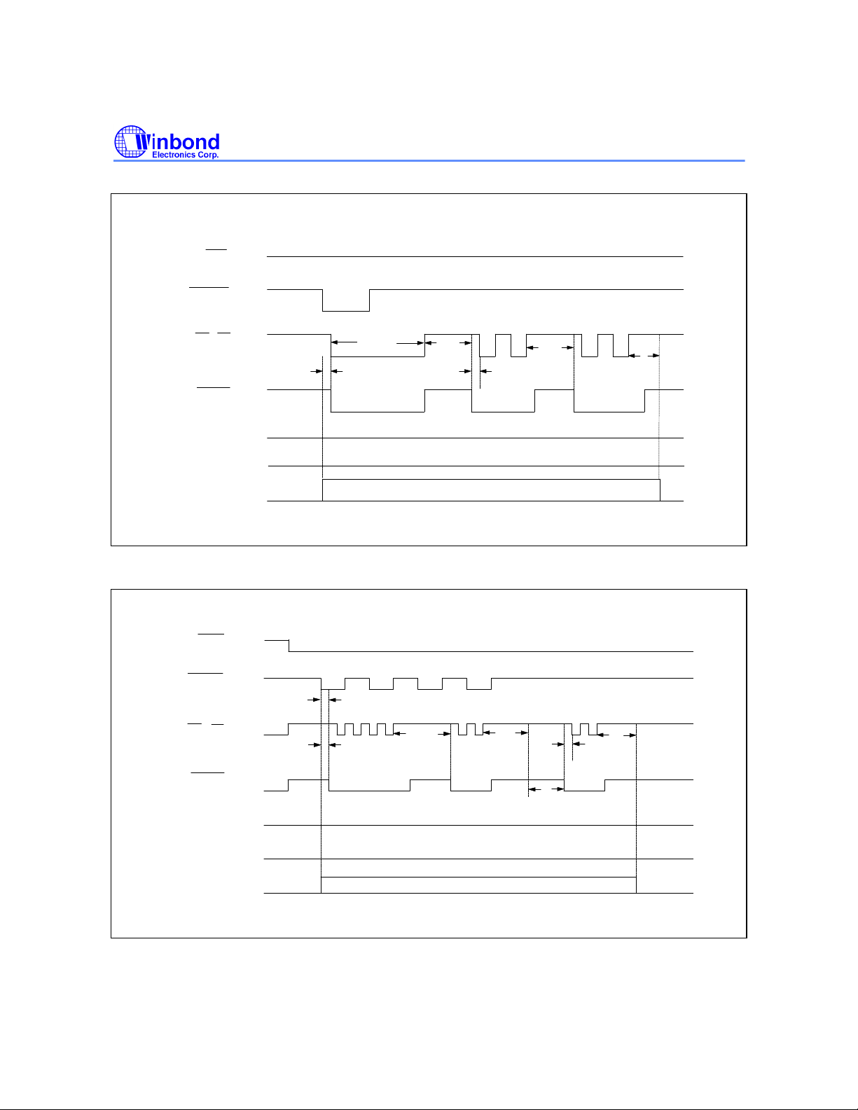
a. The one-key redialing function timing diagram is shown in Figure 4.
b. Once dialing of D1 to Dn is finished, pressing RD key will cause the pulse output pin
to go low for 2.2 seconds break time and 600 mS pause will automatically be added.
c. If the pulses of the dialed number D1 to Dn have not finished,
2. OFF HOOK , D1 , D2 , ..., Dn BUSY, Come ON HOOK , OFF HOOK
(or ON HOOK &
), RD
), D1 , D2 , ..., Dn , BUSY RD
RD key will be ignored.
the
- 6 -
Page 7
W9145 SERIES
HFI
¡õ
HFI
¡õ
HFI
¡õ
HFI
¡õ
HFI
¡õ
HFI
¡õ
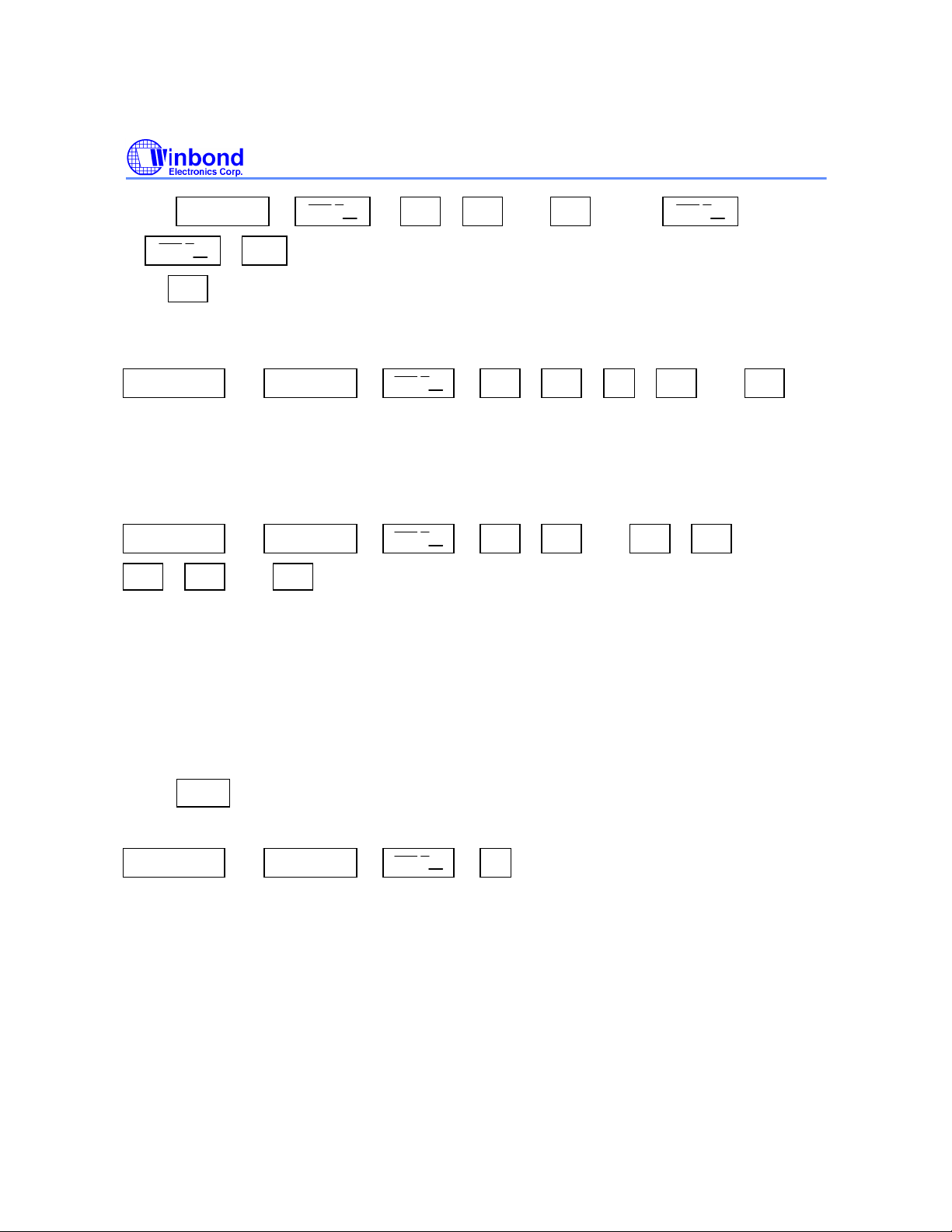
Or ( ON HOOK &
, RD
If RD is the first key after off-hook, only the redialing function will be executed and the pulse
output pin will not go low for the break time of 2.2 seconds.
), D1 , D2 , ..., Dn , BUSY,
, Come
Access Paus
OFF HOOK (or ON HOOK &
1. The pause function can be stored in memory.
2. The pause function may be executed in normal dialing, redialing, or repertory dialing.
3. The pause function timing diagram is shown in Figure 5.
), D1 , D2 , P , D3 , ..., Dn
Pulse-to-tone ( */T)
OFF HOOK (or ON HOOK &
D1' , D2' , ..., Dn'
1. If the mode switch is set to pulse mode, then the output signal will be:
D1, D2, ..., Dn, Pause (3.1S) D1', D2', ..., Dn'.
(Pulse) (Tone)
2. If the mode switch is set to tone mode, then the output signal will be:
D1, D2, ..., Dn, * , D1' , D2', ..., Dn'
(Tone) (Tone) (Tone)
3. The device can be reset to pulse mode only by going on-hook; device remains in tone mode when
the digits have been dialed out.
), D1 , D2 , ..., Dn , */T ,
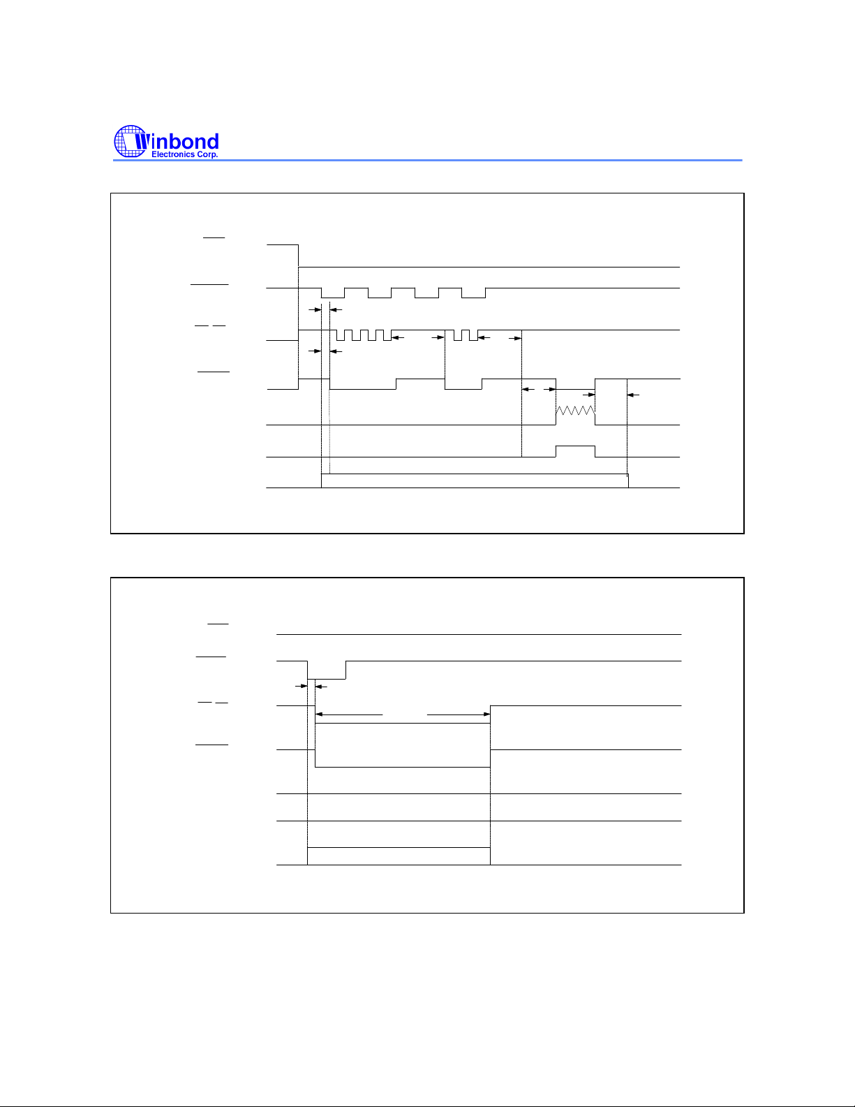
4. The
P→T
function timing diagram is shown in Figure 6.
Flash
OFF HOOK (or ON HOOK &
1. Flash key cannot be stored as a digit in memory. Flash key has first priority among keyboard
functions.
2. The system will return to the initial state after the break time is finished.
3. The flash function timing diagram is shown in Figure 7.
), F
Publication Release Date: August 1996
- 7 - Revision A4
Page 8
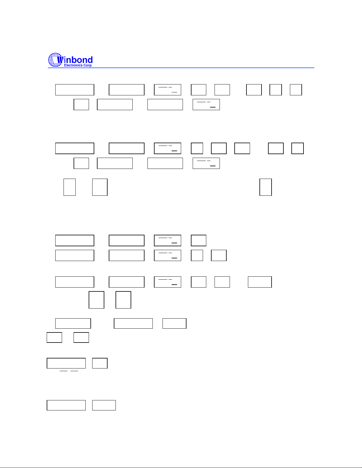
Number Store
HFI
¡õ
HFI
¡õ
HFI
¡õ
HFI
¡õ
HFI
¡õ
HFI
¡õ
HFI
¡õ
W9145 SERIES
1. OFF HOOK (or ON HOOK &
Mn (or Ln ) ON HOOK (or ON HOOK &
a. The dialing of D1, D2, ..., Dn must be finished before S key may be pressed.
b. D1, D2, ..., Dn will be stored in memory location Mn or Ln and then dialed out.
c. Mn = M1 to M3; Ln = 0 to 9, *, Pause.
2. OFF HOOK (or ON HOOK &
Mn (or Ln ) ON HOOK (or ON HOOK &
a. D1, D2, ..., Dn will be stored in memory location Mn or Ln but will not be dialed out.
b. P and */T keys can be stored as a digit in memory. In store
mode,
function key.
c. The store mode is released once the store function is completed or the state of the hook switch
changes.
), D1 , D2 , ..., Dn , S , S ,
)
), S , D1 , D2 , ..., Dn , S ,
)
P is the pause
Repertory Dialing
1. OFF HOOK (or ON HOOK &
2. OFF HOOK (or ON HOOK &
), Mn
), A , Ln
Save Key
1. OFF HOOK (or ON HOOK &
If the dialingofD1 to Dn is finished, pressing the SAVE key will cause D1 to Dn to be
duplicated to the SAVE memory.
2. ON HOOK Come OFF HOOK , SAVE
D1 to Dn will be dialed out after the SAVE key is pressed.
), D1 , D2 , ..., SAVE
Call Disconnect
OFF HOOK CD
The DP/C5 pin will go low (line break) when the CD key is pressed and the system will be reset to
initial state.
Mute Key
OFF HOOK MUTE
The mute output will be switched on as long as the MUTE key is depressed.
- 8 -
Page 9
CD and MUTE key function timing diagram is shown in Figure 8.
HFI
¡õ
HKS
HKS
Mixed Dialing
W9145 SERIES
OFF HOOK (or ON HOOK &
1. Normal dialing + Repertory dialing + Normal dialing
2. Repertory dialing + Normal dialing + Repertory dialing
3. Redialing + Normal dialing + Repertory dialing
a. Redialing and SAVE dialing are valid for first key-in only.
b. The second sequence should not be performed until the first sequence is dialed out completely.
),
ABSOLUTE MAXIMUM RATINGS
PARAMETER SYMBOL RATING UNIT
DC Supply Voltage
Input/Output Voltage VIL VSS -0.3 V
Power Dissipation PD 120 mW
Operating Temperature TOPR -20 to +70
VDD−VSS
VIH VDD +0.3 V
VOL VSS -0.3 V
VOH VDD +0.3 V
-0.3 to +7.0 V
°C
Storage Temperature TSTG -55 to +150
Note: Exposure to conditions beyond those listed under Absolute Maximum Ratings may adversely affect the life and reliability of the
device.
°C
DC CHARACTERISTICS
VDD = 2.5V, FOSC = 3.58 MHz, TA = 25° C, unless otherwise noted
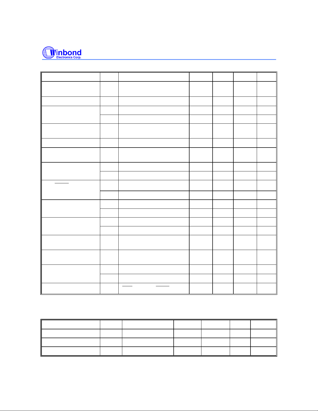
PARAMETER SYM. CONDITIONS MIN. TYP. MAX. UNIT
Operating Voltage VDD Tone 2.0 - 5.5 V
Pulse 2.0 - 5.5 V
Operating Current IOP Tone, Unloaded - 0.6 2 mA
Pulse, Unloaded - 0.2 0.5 mA
Memory Retention IMR
Standby Current IS
Tone Output VTO
= 1, TA = 25° C
VDD = 1.0V
= 0, VDD = 2.5V
Row Group, RL = 5 KΩ
- 9 - Revision A4
- 0.1 0.2
- 0.1 5
130 150 170 Vrms
Publication Release Date: August 1996
µA
µA
Page 10
W9145 SERIES
MUTE
HKS
TEST
DC Characteristics, continued
PARAMETER SYM. CONDITIONS MIN. TYP. MAX. UNIT
Pre-Emphasis Column Group/Row Group
VDD = 2.0−5.5V
DTMF Distortion THD
HFO Drive/Sink IHFH VHFH = 2.0V 0.5 - - mA
Current IHFL VHFL = 0.5V 0.5 - - mA
Tone Output External
Load Impedance
Tone Output DC Level VDC
Tone Output Sink
Current
Pulse Output IPH VPO = 2.0V -0.2 - - mA
Drive/Sink Current IPL VPO = 0.5V 0.2 - - mA
T/P
Drive/Sink Current IML VMO = 0.5V 2 - - mA
Key Tone Output IKH VKO = 2.0V -0.5 - - mA
Drive/Sink Current IKL VKL = 0.5V 0.5 - - mA
X MUTE Drive/Sink ILH VLO = 2.0V -0.2 - - mA
Current IIL VLO = 0.5V 0.2 - - mA
Output
IMH VMO = 2.0V -0.2 - - mA
RL = 5 KΩ
RL
THD < -23 dB
VDD = 2.0−5.5V
ITL VTO = 0.5V 0.2 - - mA
1 2 3 dB
- -30 -23 dB
5 - -
1.0 - 3.0 V
KΩ
Input Voltage Low VIL GND - 0.3
VDD
Input Voltage High VIH 0.7
VDD
Keypad Input IKD VI = 0V 10 30 80
Drive/Sink Current IKS VI = 2.5V 200 400 Control Pin Input IIN
, MODE,
, B/M
- -
- VDD V
±25 µA
AC CHARACTERISTICS
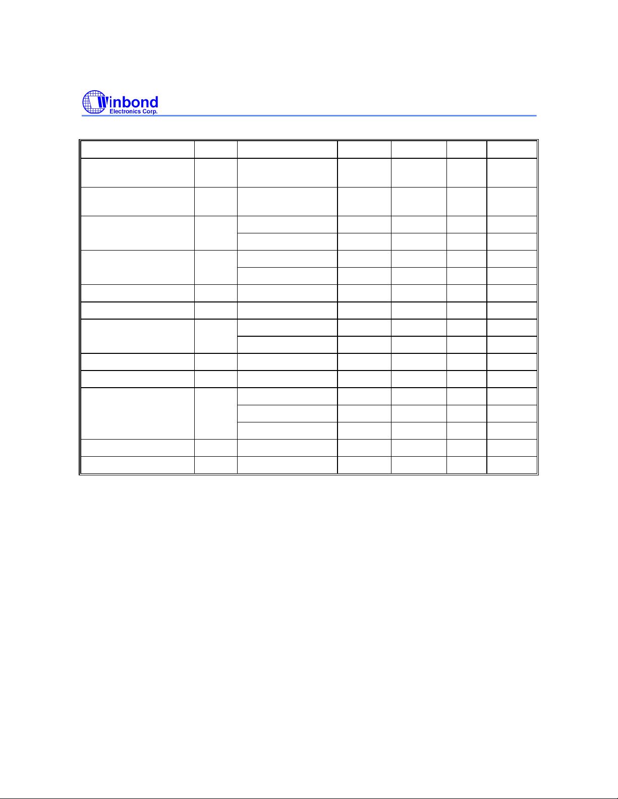
PARAMETER SYM. CONDITIONS MIN. TYP. MAX. UNIT
Key-in Debounce TKID - 20 - mS
Key-release Debounce TKRD - 20 - mS
Key tone Delay TKD - 20 - mS
- 10 -
V
µA
µA
Page 11
W9145 SERIES
AC Characteristics, continued
PARAMETER SYM. CONDITIONS MIN. TYP. MAX. UNIT
One-key Redial Break
Time
One-key Redial Break
Pause Time
Pulse Mute Delay TMD B/M = 1 - 40 - mS
Pre-digit Pause TPDP B/M = 1 - 40 - mS
Pulse Rate TPR Mode = 1 - 10 - ppS
Interdigit Pause TIDP - 800 - mS
Make/Break Ratio M:B B/M = 1 - 40:60 - %
Tone Duration TTD Auto Dialing - 93 - mS
Intertone Pause TITP Auto Dialing - 93 - mS
Flash Break Time TFB F1 - 98 - mS
Pause Time TP - 3.1 - S
TRB - 2.2 - S
TRP - 600 - mS
B/M = 0 - 33.3 - mS
B/M = 0 - 33.3 - mS
B/M = 0 - 33.3:66.7 - %
F2 - 305 - mS
F3 - 600 - mS
Key Tone Frequency f8 - 1.2 - KHz
Publication Release Date: August 1996
- 11 - Revision A4
Page 12
TIMING WAVEFORMS
HKS
W9145 SERIES
KEY IN
KT
DP/C5
T/P MUTE
DTMF
X MUTE
OSC.
HKS
KEY IN
DTMF
X MUTE
4
2
T
KID
T
T
PDP
OSCILLATION
MANUAL DIALING
IDP
T
MD
T
R
KRD
LOW
LOW
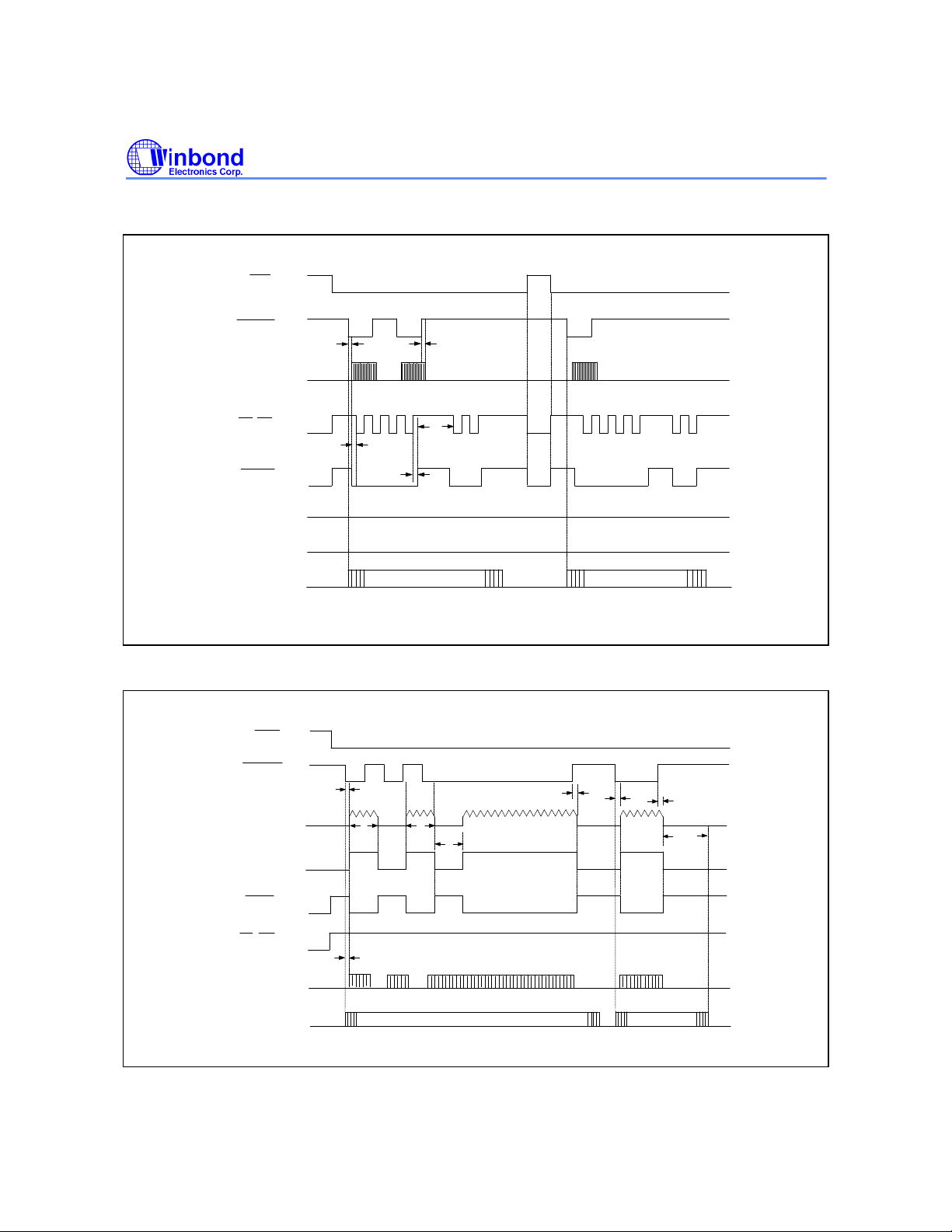
Figure 1. Pulse Mode Dialing Timing Diagram
T
KID
T
TD
T
T
ITP
TD
OSCILLATION
AUTO DIALING
T
KRD
T
KID
T
KRD
T
ITP
T/P MUTE
DP/C5
KT
OSC.
T
KD
OSCILLATION
Figure 2(a). Tone Mode Normal Dialing Diagram
- 12 -
OSCILLATION
Page 13
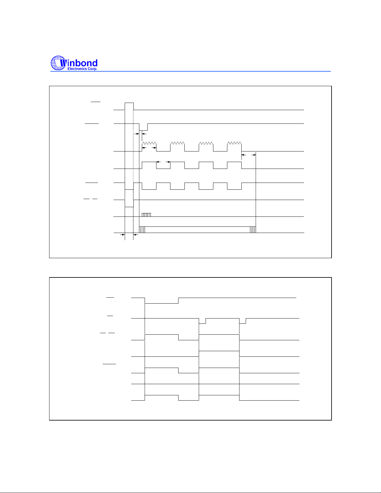
Timing Waveforms, continued
HKS
W9145 SERIES
KEY IN
DTMF
X MUTE
T/P MUTE
DP/C5
KT
OSC.
HKS
R
T
KID
T
TD
T
ITP
OSCILLATION
ON HOOK
Figure 2(b). Tone Mode Redialing Timing Diagram
OFF HOOK
ON HOOK
T
ITP
HFI
DP/C5
HFO
T/P MUTE
X MUTE
CHIP ENABLE
LOW
Figure 3(a). Handfree Function Timing Diagram
Publication Release Date: August 1996
- 13 - Revision A4
Page 14
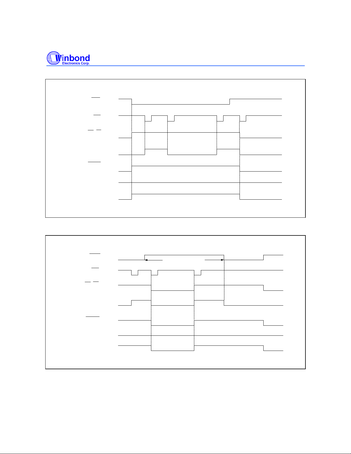
Timing Waveforms, continued
HKS
HFI
DP/C5
HFO
T/P MUTE
W9145 SERIES
X MUTE
CHIP ENABLE
HKS
HFI
DP/C5
HFO
T/P MUTE
X MUTE
LOW
Figure 3(b). Handfree Function Timing Diagram
ON HOOK
LOW
CHIP ENABLE
Figure 3(c). Handfree Function Timing Diagram
- 14 -
Page 15
Timing Waveforms, continued
HKS
W9145 SERIES
LOW
KEY IN
DP/C5
T/P MUTE
X MUTE
DTMF
OSC.
HKS
KEY IN
R
T
RB
T
KID
Figure 4. Pulse Mode Timing Diagram
2
KID
T
T
RP
LOW
LOW
OSCILLATION
P 24
M
B
T
PDP
IDP
T
B
T
IDP
DP/C5
T/P MUTE
DTMF
X MUTE
OSC.
T
PDP
Figure 5. Pause Function Timing Diagram
TIDP
LOW
LOW
OSCILLATION
TIDP
- 15 - Revision A4
T
IDP
T
IDP
IP
T
Publication Release Date: August 1996
Page 16
Timing Waveforms, continued
HKS
W9145 SERIES
KEY IN
DP/C5
T/P MUTE
DTMF
X MUTE
OSC.
HKS
KEY IN
4 2
*/T
2
TKID
T
PDP
Figure 6. P→T Operation Timing Diagram in Normal Dialing
F
T
KID
TIDP
LOW
OSCILLATION
LOW
T
IDP
T
P
T
ITP
DP/C5
T/P MUTE
X MUTE
DTMF
OSC.
T
FB
OSCILLATION
Figure 7. Flash Operation Timing Diagram
- 16 -
LOW
LOW
Page 17
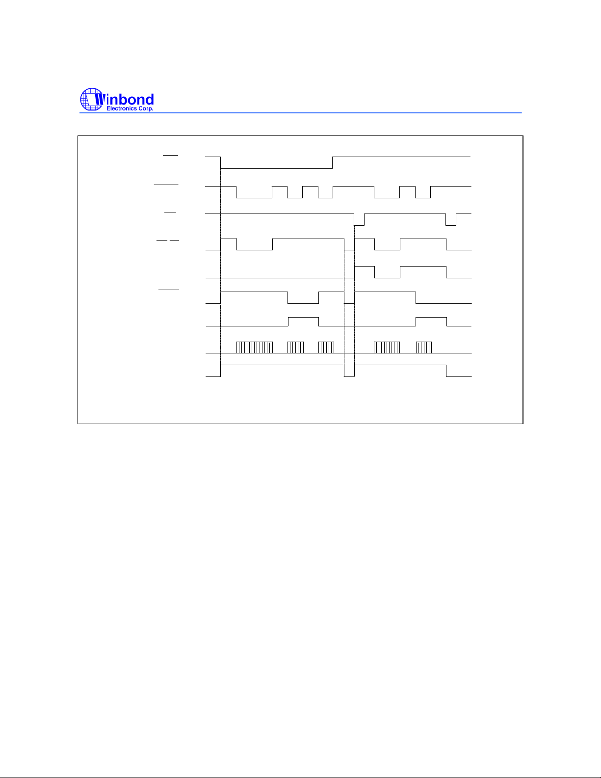
Timing Waveforms, continued
HKS
W9145 SERIES
KEY IN
HFI
DP/C5
HFO
T/P MUTE
X MUTE
KT
CHIP ENABLE
CD
Figure 8. Mute Key Operation Timing Diagram
MT
MT
CD
(MT = MUTE KEY)
MT
Publication Release Date: August 1996
- 17 - Revision A4
Page 18

W9145 SERIES
Headquarters
No. 4, Creation Rd. III,
Science-Based Industrial Park,
Hsinchu, Taiwan
TEL: 886-3-5770066
FAX: 886-3-5792697
http://www.winbond.com.tw/
Voice & Fax-on-demand: 886-2-7197006
Winbond Electronics (H.K.) Ltd.
Rm. 803, World Trade Square, Tower II,
123 Hoi Bun Rd., Kwun Tong,
Kowloon, Hong Kong
TEL: 852-27516023
FAX: 852-27552064
Taipei Office
11F, No. 115, Sec. 3, Min-Sheng East Rd.,
Taipei, Taiwan
TEL: 886-2-7190505
FAX: 886-2-7197502
Note: All data and specifications are subject to change without notice.
- 18 -
Winbond Electronics North America Corp.
Winbond Memory Lab.
Winbond Microelectronics Corp.
Winbond Systems Lab.
2730 Orchard Parkway, San Jose,
CA 95134, U.S.A.
TEL: 1-408-9436666
FAX: 1-408-9436668
 Loading...