

Page 1

W90P710CD/W90P710CDG
32-BIT ARM7TDMI-BASED MCU
W90P710CD/W90P710CDG
16/32-bit ARM microcontroller
Product Data Sheet
Publication Release Date: September 19, 2006
- 1 - Revision B2
Page 2

W90P710CD/W90P710CDG
Revision History
REVISION DATE COMMENTS
A 2005/12/02 Draft
A.1 2005/12/21 Modify the register definition
A.2 2006/01/17 Modify SD description
Update LCD C version design spec.
A.3 2006/07/07
B 2006/07/26
Update Smartcard C version design spec.
Add RTC 32.768K clock measurment apllication note.
Add RTC application note.
Change EBI SDRAM control register SDCONFx[13] AUTOPR
definition.
Modify LCD register map section 7.2.2
Change 2 to 1 slave/device select lines
Change SDIO to SD
Add Electrical specification
SDO change to SD page 11
SDIO change to SD page 33
“W99P710” change to “W90P710” page 245
B1 2006/08/08
B2 2006/09/19 Delete section 6
Delete “it is same as the UART of W99740” page 333
Delete “it is same as the UART of W99702” page 332
Delete “note” page 337,338
ADD USB WakeUp control bit
Update table 5.2
- 2 -
Page 3

W90P710CD/W90P710CDG
Table of Contents-
1. GENERAL DESCRIPTION ......................................................................................................... 6
2. FEATURES ................................................................................................................................. 6
3. PIN DIAGRAM .......................................................................................................................... 13
4. PIN ASSIGNMENT ................................................................................................................... 14
5. PIN DESCRIPTION................................................................................................................... 20
6. FUNCTIONAL DESCRIPTION ................................................................................................. 33
6.1 ARM7TDMI CPU CORE ............................................................................................... 33
6.2 System Manager........................................................................................................... 34
6.2.1 Overview ......................................................................................................................34
6.2.2 System Memory Map....................................................................................................34
6.2.3 Address Bus Generation ..............................................................................................37
6.2.4 Data Bus Connection with External Memory ................................................................37
6.2.5 Bus Arbitration..............................................................................................................46
6.2.6 Power management .....................................................................................................47
6.2.7 Power-On Setting .........................................................................................................49
6.2.8 System Manager Control Registers Map......................................................................50
6.3 External Bus Interface .................................................................................................. 64
6.3.1 EBI Overview................................................................................................................64
6.3.2 SDRAM Controller ........................................................................................................64
6.3.3 EBI Control Registers Map ........................................................................................... 68
6.4 Cache Controller........................................................................................................... 86
6.4.1 On-Chip RAM ............................................................................................................... 86
6.4.2 Non-Cacheable Area .................................................................................................... 86
6.4.3 Instruction Cache..........................................................................................................87
6.4.4 Data Cache ..................................................................................................................89
6.4.5 Write Buffer ..................................................................................................................91
6.4.6 Cache Control Registers Map.......................................................................................91
6.5 Ethernet MAC Controller............................................................................................... 97
6.5.1 EMC Functional Description ......................................................................................... 98
6.5.2 EMC Register Mapping ..............................................................................................108
6.6 GDMA Controller ........................................................................................................ 161
6.6.1 GDMA Functional Description ....................................................................................161
6.6.2 GDMA Register Map ..................................................................................................162
6.7 USB Host Controller ................................................................................................... 171
6.7.1 USB Host Functional Description ...............................................................................171
6.7.2 USB Host Controller Registers Map ...........................................................................172
6.7.3 HCCA .........................................................................................................................194
6.7.4 Endpoint Descriptor ....................................................................................................194
6.7.5 Transfer Descriptor..................................................................................................... 194
6.8 USB Device Controller................................................................................................ 194
Publication Release Date: September 19, 2006
- 3 - Revision B2
Page 4

W90P710CD/W90P710CDG
6.8.1 USB Endpoints ...........................................................................................................195
6.8.2 Standard device request.............................................................................................195
6.8.3 USB Device Register Description ...............................................................................195
6.9 SD Host Controller...................................................................................................... 234
6.9.1 Functional Description ................................................................................................234
6.9.2 Register Mapping .......................................................................................................236
6.9.3 SD Register Description .............................................................................................237
6.10 LCD Controller ............................................................................................................ 253
6.10.1 Main Features ............................................................................................................253
6.10.2 LCD Register MAP .....................................................................................................254
6.10.3 LCD Special Register Description ..............................................................................256
6.11 Audio Controller .......................................................................................................... 307
6.11.1 IIS Interface ................................................................................................................307
6.11.2 AC97 Interface ...........................................................................................................308
6.11.3 Audio Controller Register Map....................................................................................311
6.12 Universal Asynchronous Receiver/Transmitter Controller ......................................... 330
6.12.1 UART0........................................................................................................................332
6.12.2 UART1........................................................................................................................332
6.12.3 UART2........................................................................................................................334
6.12.4 UART3........................................................................................................................336
6.12.5 General UART Controller ...........................................................................................337
6.12.6 High speed UART Controller ......................................................................................350
6.13 Timer/Watchdog Controller......................................................................................... 364
6.13.1 General Timer Controller ............................................................................................ 364
6.13.2 Watchdog Timer .........................................................................................................364
6.13.3 Timer Control Registers Map...................................................................................... 364
6.14 Advanced Interrupt Controller..................................................................................... 372
6.14.1 Interrupt Sources........................................................................................................373
6.14.2 AIC Registers Map .....................................................................................................376
6.15 General-Purpose Input/Output ................................................................................... 389
6.15.1 GPIO Control Registers Map......................................................................................392
6.15.2 GPIO Register Description .........................................................................................393
6.16 Real Time Clock ......................................................................................................... 424
6.16.1 RTC Register Map...................................................................................................... 426
6.16.2 RTC Application Note ................................................................................................. 439
6.17 Smart Card Host Interface .......................................................................................... 440
6.17.1 Register Mapping .......................................................................................................440
6.17.2 Register Description ...................................................................................................442
6.17.3 Functional description.................................................................................................468
6.18 I2C Interface ............................................................................................................... 471
6.18.1 I2C Protocol ................................................................................................................472
6.18.2 I2C Serial Interface Control Registers Map ................................................................475
- 4 -
Page 5

W90P710CD/W90P710CDG
Universal Serial Interface............................................................................................ 483
6.19
6.19.1 USI Timing Diagram ...................................................................................................483
6.19.2 USI Registers Map .....................................................................................................484
6.20 PWM ........................................................................................................................... 491
6.20.1 PWM double buffering and reload automatically ........................................................491
6.20.2 Modulate Duty Ratio...................................................................................................492
6.20.3 Dead Zone Generator.................................................................................................492
6.20.4 PWM Timer Start procedure.......................................................................................493
6.20.5 PWM Timer Stop procedure ....................................................................................... 493
6.20.6 PWM Register Map ....................................................................................................494
6.21 Keypad Interface......................................................................................................... 502
6.21.1 KeyPad Interface Register Map.................................................................................. 503
6.21.2 Register Description ...................................................................................................504
6.22 PS2 Host Interface Controller..................................................................................... 511
6.22.1 PS2 Host Controller Interface Register Map...............................................................512
6.22.2 Register Description ...................................................................................................512
7. ELECTRICAL SPECIFICATIONS........................................................................................... 516
7.1 Absolute Maximum Ratings ........................................................................................ 516
7.2 DC Specifications ....................................................................................................... 516
7.2.1 Digital DC Characteristics...........................................................................................516
7.2.2 USB Transceiver DC Characteristics..........................................................................518
7.3 AC Specifications........................................................................................................ 518
7.3.1 EBI/SDRAM Interface AC Characteristics ..................................................................518
7.3.2 EBI/(ROM/SRAM/External I/O) AC Characteristics .................................................... 519
7.3.3 USB Transceiver AC Characteristics.......................................................................... 520
7.3.4 EMC RMII AC Characteristics ....................................................................................521
7.3.5 LCD Interface AC Characteristics............................................................................... 523
7.3.6 SD Interface AC Characteristics.................................................................................524
7.3.7 AC97/I2S Interface AC Characteristics.......................................................................525
7.3.8 Smart Card Interface AC Characteristics....................................................................527
7.3.9 I2C Interface AC Characteristics ................................................................................528
7.3.10 USI Interface AC Characteristics................................................................................529
7.3.11 PS2 Interface AC Characteristics ...............................................................................531
8. ORDERING INFORMATION .................................................................................................. 532
9. PACKAGE SPECIFICATIONS................................................................................................ 533
10. APPENDIX A: W90P710 REGISTERS MAPPING TABLE..................................................... 534
Publication Release Date: September 19, 2006
- 5 - Revision B2
Page 6

W90P710CD/W90P710CDG
1. GENERAL DESCRIPTION
The W90P710 is built around an outstanding CPU core, the 16/32 ARM7TDMI RISC processor which
designed by Advanced RISC Machines, Ltd. It offers 4K-byte I-cache/SRAM and 4K-byte Dcache/SRAM, is a low power, general purpose integrated circuits. Its simple, elegant, and fully static
design is particularly suitable for cost sensitive and power sensitive applications.
One 10/100 Mb MAC of Ethernet controller is built-in to reduce total system cost. A LCD controller is
also built-in to support TFT and low cost STN LCD modules.
With one USB 1.1 host controller, one USB 1.1 device controller, two smart card host controller, four
independent UARTs, one Watchdog timer, up to 71 programmable I/O ports, PS/2 keyboard controller
and an advanced interrupt controller, the W90P710 is particularly suitable for point-of-sale (POS),
access control and data collector.
The W90P710 also provides one AC97/I²S controller, one SD host controller, one 2-Channel GDMA,
two 24-bit timers with 8-bit pre-scale, The external bus interface (EBI) controller provides for SDRAM,
ROM/SRAM, flash memory and I/O devices. The System Manager includes an internal 32-bit system
bus arbiter and a PLL clock controller. With a wide range of serial communication and Ethernet
interfaces, the W90P710 is also suitable for communication gateways as well as many other general
purpose applications.
2. FEATURES
Architecture
y Fully 16/32-bit RISC architecture
y Little/Big-Endian mode supported
y Efficient and powerful ARM7TDMI core
y Cost-effective JTAG-based debug solution
External Bus Interface
y 8/16/32-bit external bus support for ROM/SRAM, flash memory, SDRAM and external I/Os
y Support for SDRAM
y Programmable access cycle (0-7 wait cycle)
y Four-word depth write buffer for SDRAM write data
y Cost-effective memory-to-peripheral DMA interface
Instruction and Data Cache
y Two-way, Set-associative, 4K-byte I-cache and 4K-byte D-cache
y Support for LRU (Least Recently Used) Protocol
y Cache can be configured as internal SRAM
y Support Cache Lock function
- 6 -
Page 7

Ethernet MAC Controller
y DMA engine with burst mode
y MAC Tx/Rx buffers (256 bytes Tx, 256 bytes Rx)
y Data alignment logic
y Endian translation
y 100/10-Mbit per second operation
y Full compliance with IEEE standard 802.3
y RMII interface only
y Station Management Signaling
y On-Chip CAM (up to 16 destination addresses)
y Full-duplex mode with PAUSE feature
y Long/short packet modes
y PAD generation
LCD Controller (LCDC)
W90P710CD/W90P710CDG
(1) STN LCD Display
y Supports 4-bit single scan Monochrome STN LCD panel, 8-bit single scan Monochrome STN LCD
panel, 8-bit single scan Color STN LCD panel
y Up to 16 gray levels display for Monochrome STN LCD panel
y Up to 4096(12bpp) colors display for Color STN LCD panel
y Virtual coloring method: Frame Rate Control (16-level)
y Anti-flickering method: Time-based Dithering
(2) TFT LCD Display
y Supports Sync-type TFT LCD panel and Sync-type High-color TFT LCD panel
y Supports direct or palettized color display
(3) TV Encoder
y Supports 8-bit YCbCr data output format to connect with external TV Encoder
(4) LCD Preprocessing
y Supports RGB Raw-data or packetd YUV422 format
y Programmable parameters for different image size
y Build in two FIFOs, FIFO 1 is for Video image and FIFO 2 is for OSD image. Each FIFO is 16
words deep
Publication Release Date: September 19, 2006
- 7 - Revision B2
Page 8

W90P710CD/W90P710CDG
(5) LCD Post processing
y Support for one OSD (On-Screen-Display) overlay
y Support various OSD function
y Programmable parameters for different display panel
(6) Others
y Color-look up table size 256x32 bit for TFT used when displaying 1bpp, 2bpp, 4bpp, 8bpp image
y Dedicated DMA for block transfer mode
DMA Controller
y 2-channel General DMA for memory-to-memory data transfers without CPU intervention
y Initialed by a software or external DMA request
y Increments or decrements a source or destination address in 8-bit, 16-bit or 32-bit data transfers
y 4-data burst mode
UART
y Four UART (serial I/O) blocks with interrupt-based operation
y Support for 5-bit, 6-bit, 7-bit or 8-bit serial data transmit and receive
y Programmable baud rates
y 1, ½ or 2 stop bits
y Odd or even parity
y Break generation and detection
y Parity, overrun and framing error detection
y X16 clock mode
y UART1 supports Bluetooth, and UART2 supports IrDA1.0 SIR
Timers
y Two programmable 24-bit timers with 8-bit pre-scaler
y One programmable 20 bit with selectable additional 8-bit prescaler Watchdog timer
y One-shot mode, periodical mode or toggle mode operation
Programmable I/Os
y 71 programmable I/O ports
y Pins individually configurable to input, output or I/O mode for dedicated signals
y I/O ports are configurable for Multiple functions
- 8 -
Page 9

W90P710CD/W90P710CDG
Advanced Interrupt Controller
y 31 interrupt sources, including 6 external interrupt sources
y Programmable normal or fast interrupt mode (IRQ, FIQ)
y Programmable as either edge-triggered or level-sensitive for 6 external interrupt sources
y Programmable as either low-active or high-active for 6 external interrupt sources
y Priority methodology is encoded to allow for interrupt daisy-chaining
y Automatically mask out the lower priority interrupt during interrupt nesting
USB Host Controller
y USB 1.1 compliant
y Compatible with Open HCI 1.0 specification
y Supports low-speed and full speed devices
y Build-in DMA for real time data transfer
y Two on-chip USB transceivers with one optionally shared with USB Device Controller
USB Device Controller
y USB 1.1 compliant
y Support four USB endpoints including one control endpoint and 3 configurable endpoints for rich
USB functions
Two PLLs
y The external clock can be multiplied by on-chip PLL to provide high frequency system clock
y The input frequency range is 3-30MHz; 15MHz is preferred.
y One PLL for both CPU and USB host/device controller
y One PLL for LCD pixel clock and audio IIS 12.288/16.934MHz clock source
y Programmable clock frequency
Real Time Clock (RTC)
y 32.768KHz operation
y Time counter (second, minute, hour) and calendar counter (day, month, year)
y Alarm register (second, minute, hour, day, month, year)
y 12 or 24-hour mode selectable
y Recognize leap year automatically
y Day of the week counter
y Frequency compensate register (FCR)
y Beside FCR, all clock and alarm data expressed in BCD code
y Support tick time interrupt
Publication Release Date: September 19, 2006
- 9 - Revision B2
Page 10

W90P710CD/W90P710CDG
4-Channel PWM
y Four 16-bit timers with PWM
y Two 8-bit pre-scalers & Two 4-bit dividers
y Programmable duty control of output waveform
y Auto reload mode or one-shot pulse mode
y Dead-zone generator
I2C Master
y Two Channel I2C
y Compatible with Philips I
y Support multi master operation
y Clock stretching and wait state generation
y Provide multi-byte transmit operation, up to 4 bytes can be transmitted in a single transfer
y Software programmable acknowledge bit
y Arbitration lost interrupt, with automatic transfer cancellation
y Start/Stop/Repeated Start/Acknowledge generation
y Start/Stop/Repeated Start detection
y Bus busy detection
y Supports 7 bit addressing mode
y Software mode I
2
C
2
C standard, support master mode only
Universal Serial Interface (USI)
y 1-Channel USI
y Support USI (Microwire/SPI) master mode
y Full duplex synchronous serial data transfer
y Variable length of transfer word up to 32 bits
y Provide burst mode operation, transmit/receive can be executed up to four times in one transfer
y MSB or LSB first data transfer
y Rx and Tx on both rising or falling edge of serial clock independently
y Two slave/device select lines
y Fully static synchronous design with one clock domain
2-Channel AC97/I2S Audio Codec Host Interface
y AHB master port and an AHB slave port are offered in audio controller.
y Always 8-beat incrementing burst
y Always bus lock when 8-beat incrementing burst
- 10 -
Page 11

W90P710CD/W90P710CDG
y When reach middle and end address of destination address, a DMA_IRQ is requested to CPU
automatically
Smart Card Host Interface (SCHI)
y ISO-7816 compliant
PC/SC T=0, T=1 compliant
y
16-byte transmitter FIFO and 16-byte receiver FIFO
y
y FIFO threshold interrupt to optimize system performance
y Programmable transmission clock frequency
Versatile baud rate configuration
y
y UART-like register file structure
y General-purpose C4, C8 channels
SD Host Interface
y Directly connect to Secure Digital (SD, MMC) flash memory card.
y Supports DMA function to accelerate the data transfer between the internal buffer, external
SDRAM, and flash memory card.
y Two 512 bytes internal buffers are embedded inside the controller.
y No SPI mode.
KeyPad Scan Interface
y Scan up to 16 rows by 8 columns with an external 4 to 16 decoder and 4 rows by 8 columns array
without auxiliary component
y Programmable debounce time
y One or two keys scan with interrupt and three keys reset function.
y Wakeup CPU from IDEL/Power Down mode
PS2 Host Interface
y APB slave consisted of PS2 protocol.
y Connect IBM keyboard or bar-code reader through PS2 interface.
y Provide hardware scan code to ASCII translation
Power management
y Programmable clock enables for individual peripheral
y IDLE mode to halt ARM Core and keep peripheral working
y Power-Down mode to stop all clocks included external crystal oscillator.
y Exit IDLE by all interrupts
y Exit Power-Down by keypad,USB device and external interrupts
Publication Release Date: September 19, 2006
- 11 - Revision B2
Page 12

Operation Voltage Range
y 3.0 ~ 3.6 V for IO Buffer
y 1.62 ~ 1.98 V for Core Logic
Operation Temperature Range
y TBD
Operating Frequency
y Up to 80 MHz
Package Type
y 176-pin LQFP
W90P710CD/W90P710CDG
- 12 -
Page 13
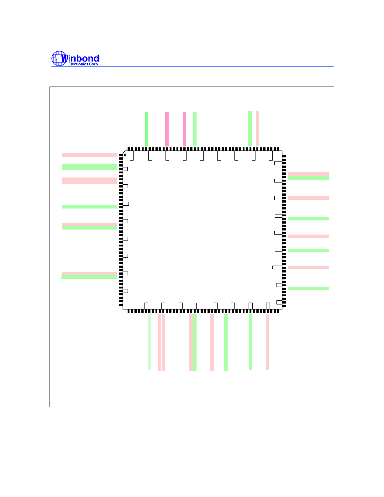
3. PIN DIAGRAM
D[0]/TBUS[0]
D[1]/TBUS[1]
D[2]/TBUS[2]
D[3]/TBUS[3]
D[4]/TBUS[4]
D[5]/TBUS[5]
VSS33
D[6]/TBUS[6]
D[7]/TBUS[7]
D[8]/TBUS[8]
D[9]/TBUS[9]
VDD33
D[10]/TBUS[10]
D[11]/TBUS[11]
D[12]/TBUS[12]
W90P710CD/W90P710CDG
nWBE[3]/SDQM[3]/GPIO[68]
nWBE[2]/SDQM[2]/GPIO[69]
D[22]/VD[14]/GPIO[58]
D[20]/VD[12]/GPIO[56]
D[21]/VD[13]/GPIO[57]
D[19]/VD[11]/GPIO[55]
D[23]/VD[15]/GPIO[59]
D[18]/VD[10]/GPIO[54]
D[17]/VD[9]/GPIO[53]
D[13]/TBUS[13]
VDD18
D[14]/TBUS[14]
D[16]/VD[8]/GPIO[52]
D[15]/TBUS[15]
VSS18
nIRQ[3]/GPIO[19]
nIRQ[2]/GPIO[18]
nWBE[0]/SDQM[0]
nWBE[1]/SDQM[1]
nSCS[1]
nSCS[0]
VDD33
nSCAS
VSS33
nSRAS
MCLK
nWE
nBTCS
MCKE
USB1VDD
DP1
DN1
USB1VSS
USB0VSS
DN0
DP0
USB0VDD
VDD33
TXD0/GPIO[5]
RXD0/GPIO[6]
TXD1/GPIO[7]
CTS1/TXD2(IrDA)/PS2_CLK/GPIO[9]
RTS1/RXD2(IrDA)/PS2_DATA/GPIO[10]
SCL0/SFRM/TIMER0/GPIO[11]
SDA0/SSPTXD/TIMER1/GPIO[12]
SCL1/SCLK/KPI_ROW[3]/GPIO[13]
SDA1/SSPRXD/KPI_ROW[2]/GPIO[14]
KPI_ROW[0]/VCLK/GPIO[30]
KPI_ROW[1]/VDEN/GPIO[31]
KPI_ROW[2]/VSYNC/GPIO[32]
KPI_ROW[3]/HSYNC/GPIO[33]
KPI_COL[7]/VD[7]/GPIO[41]
KPI_COL[6]/VD[6]/GPIO[40]
KPI_COL[5]/VD[5]/GPIO[39]
KPI_COL[4]/VD[4]/GPIO[38]
KPI_COL[3]/VD[3]/GPIO[37]
KPI_COL[2]/VD[2]/GPIO[36]
KPI_COL[1]/VD[1]/GPIO[35]
KPI_COL[0]/VD[0]/GPIO[34]
RXD1/GPIO[8]
VSS33
VDD18
VSS18
VDD33
VSS33
nRESET
TEST
PLL0VDD18
PLL0VSS18
PLL1VSS18
PLL1VDD18
nIRQ[0]/GPIO[16]
nIRQ[1]/GPIO[17]
165
160
155
SC0_CLK/SD_CLK/VD[16]/GPIO[28]
SC0_RST/SD_DAT0/VD[15]/GPIO[27]
VDD33
SC0_PRES/SD_DAT1/VD[14]/GPIO[26]
150
70
SC1_CLK/SD_PWR/VD[11]/GPIO[23]
SC0_PWR/SD_DAT2/VD[13]/GPIO[25]
SC1_DAT/SD_DAT3/VD[12]/GPIO[24]
SC1_RST/SD_CD/VD[10]/GPIO[22]
VSS33
75
SC1_PRES/nXDREQ/VD[9]GPIO[21]
175
170
5
10
15
20
25
30
35
40
TDO
TMS
TCK
TDI
W90P710
176 -pin
LQFP
50
55
60
VDD18
AC97_SYNC/I2S_LRCLK/PWM[2]/TXD3/GPIO[3]
VDD33
RTCVDD18
AC97_DATAI/I2S_DATAI/PWM[0]/DTR3/GPIO[1]
XTAL32 (32.768K)
EXTAL32 (32.768K)
AC97_nRESET/I2S_MCLK/GPIO[0]
AC97_DATAO/I2S_DATAO/PWM[1]/DSR3/GPIO[2]
AC97_BITCLK/I2S_BITCLK/PWM[3]/RXD3/GPIO[4]
nTRST
nWDOG/GPIO[15]
XTAL(15M)
VSS33
EXTAL(15M)
65
SC0_DAT/SD_CMD/VD[17]/[GPIO[29]
VSS18
145
80
PHY_RXD[0]/GPIO[44]/KPI_COL[2]/VD[10]
PHY_RXERR/GPIO[42]/KPI_COL[0]/VD[8]
SC1_PWR/nXDACK/VD[8]/GPIO[20]
VSS33
PHY_CRSDV/GPIO[43]/KPI_COL[1]/VD[9]
140
135
85
PHY_TXD[0]/GPIO[48]/KPI_COL[6]/VD[14]
PHY_TXD[1]/GPIO[49]/KPI_COL[7]/VD[15]
PHY_TXEN/GPIO[47]/KPI_COL[5]/VD[13]
PHY_REFCLK/GPIO[46]/KPI_COL[4]/VD[12]
PHY_RXD[1]/GPIO[45]/KPI_COL[3]/VD[11]
VDD33
nWAIT/TREQB
nOE
nECS[0]
130
nECS[1]
nECS[2]
VDD33
VSS33
125
nECS[3]
D[24]/VD[16]/GPIO[60]
D[25]/VD[17]/GPIO[61]
D[26]/VD[18]/GPIO[62]
D[27]/VD[19]/GPIO[63]
120
VDD33
D[28]/VD[20]/GPIO[64]
D[29]/VD[21]/GPIO[65]
D[30]/VD[22]/GPIO[66]
D[31]/VD[23]/GPIO[67]
A[21]
115
VSS33
A[20]
A[19]
A[18]
110
A[17]/TREQA
VDD18
A[16]/TACK
A[15]/TBUS[31]
A[14]/TBUS[30]
105
VSS18
A[13]/TBUS[29]
A[12]/TBUS[28]
A[11]/TBUS[27]
A[10]/TBUS[26]
100
VDD33
A[9]/TBUS[25]
A[8]/TBUS[24]
A[7]/TBUS[23]
A[6]/TBUS[22]
95
A[5]/TBUS[21]
VSS33
A[4]/TBUS[20]
A[3]/TBUS[19]
A[2]/TBUS[18]
90
A[1]/TBUS[17]
A[0]/TBUS[16]
PHY_MDIO/GPIO[50]/KPI_ROW[0]/VD[16]
PHY_MDC/GPIO[51]/KP_ROW[1]/VD[17]
Fig 3.1 Pin Diagram
Publication Release Date: September 19, 2006
- 13 - Revision B2
Page 14
W90P710CD/W90P710CDG
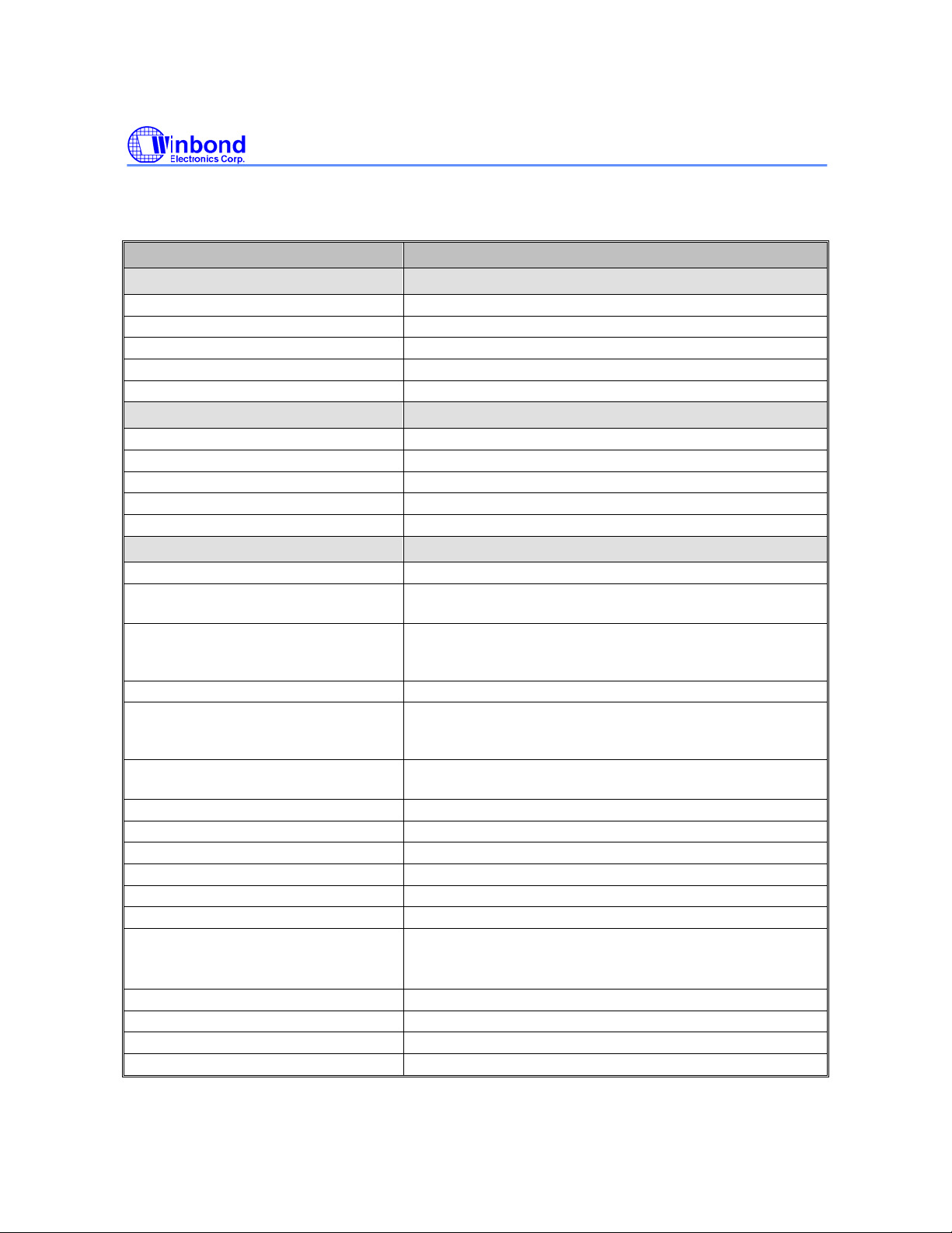
4. PIN ASSIGNMENT
Table 4.1 W90P710 Pins Assignment
PIN NAME 176-PIN LQFP
Clock & Reset ( 5 pins )
EXTAL (15M) 52
XTAL (15M) 53
EXTAL32 (32.768K) 57
XTAL32 (32.768K) 56
nRESET 37
JTAG Interface ( 5 pins )
TMS 45
TDI 46
TDO 47
TCK 48
nTRST 49
External Bus Interface ( 72 pins )
A [21] 115
A [20:0]
D [31:16] /
VD [23:8] /
GPIO [67:52]
D [15:0] 158,159,161-164, 166-170,172-176
nWBE [3:2] /
SDQM [3:2] /
GPIO[69:68]
nWBE [1;0] /
SDQM [1:0]
nSCS [1:0] 136,135
nSRAS 137
nSCAS 138
MCKE 134
nSWE 142
MCLK 140
nWAIT/
GPIO[70] /
nIRQ5
nBTCS 133
nECS [3] 125
nECS [2:0] 128-130
nOE 131
113-110,108-106,
104-101,99-95, 93-89
116-119,121-124, 149-156
146,145
144,143
132
- 14 -
Page 15

W90P710CD/W90P710CDG
Table 4.1 W90P710 Pins Assignment (Continued)
PIN NAME 176-PIN LQFP
Ethernet Interface ( 10 pins )
PHY_MDC /
GPIO [51] / KPROW[1] /
VD[17]
PHY_MDIO /
GPIO [50] /
KPROW[0] /
LD[16]
PHY_TXD [1:0] /
GPIO[49:48] /
KPCOL[7:6] /
VD[15:14]
PHY_TXEN /
GPIO [47] /
KPCOL[5] /
VD[13]
PHY_REFCLK /
GPIO [46] /
KPCOL[4] /
VD[12]
PHY_RXD [1:0] /
GPIO [45:44] /
KPCOL[3:2] /
VD[11:10]
PHY_CRSDV /
GPIO [43] /
KPCOL[1] /
VD[9]
PHY_RXERR /
GPIO [42] /
KPCOL[0] /
VD[8]
AC97/I2S/PWM/UART3 ( 5 pins )
AC97_nRESET /
I2S_MCLK /
GPIO [0] /
USB_PWREN
88
87
86,84
83
82
81,79
78
77
58
Publication Release Date: September 19, 2006
- 15 - Revision B2
Page 16
W90P710CD/W90P710CDG
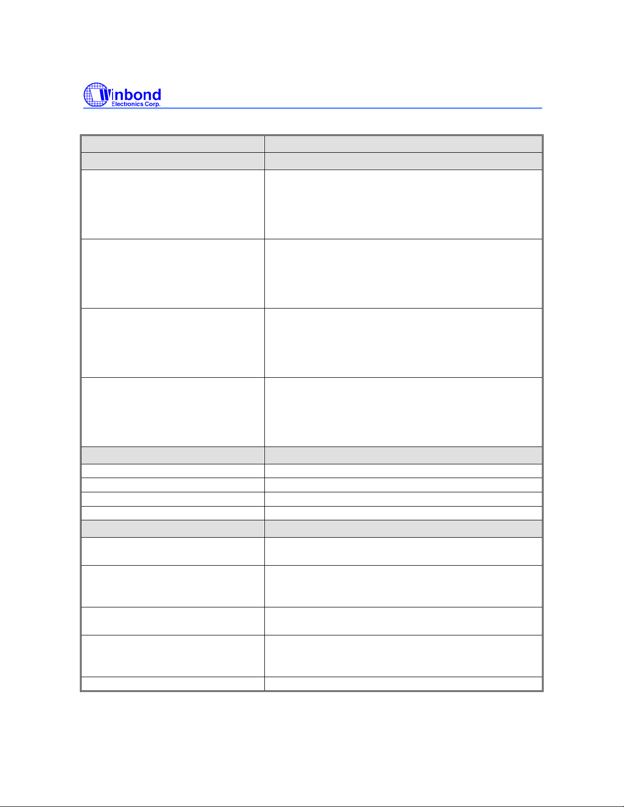
Table 4.1 W90P710 Pins Assignment (Continued)
PIN NAME 176-PIN LQFP
AC97/I2S/PWM/UART3 ( 5 pins )
AC97_DATAI /
I2S_DATAI /
PWM [0] /
DTR3 /
GPIO [1]
AC97_DATAO /
I2S_DATAO /
PWM [1] /
DSR3 /
GPIO [2]
AC97_SYNC /
I2S_LRCLK /
PWM [2] /
TXD3 /
GPIO [3]
AC97_BITCLK /
I2S_BITCLK /
PWM [3] /
RXD3
GPIO [4]
USB Interface ( 4 pins )
DP0 7
DN 0 6
DP1 2
DN1 3
Miscellaneous ( 7 pins )
nIRQ [3:2] /
GPIO [19:18]
nIRQ [1] /
GPIO [17] /
USB_OVRCUR
nIRQ [0] /
GPIO [16]
nWDOG /
GPIO [15] /
USB_PWREN
RTCVDD18 55
59
60
61
62
148,147
44
43
50
- 16 -
Page 17

W90P710CD/W90P710CDG
Table 4.1 W90P710 Pins Assignment (Continued)
NAME 176-PIN LQFP
I2C/USI(Microwire/SPI) ( 4 pins )
SCL0 /
SFRM /
Timer0 /
GPIO [11]
SDA0 /
SSPTXD /
Timer1 /
GPIO [12]
SCL1 /
SCLK /
GPIO [13] /
KPROW[3]
SDA1 /
SSPRXD /
GPIO [14] /
KPROW[2]
UART0/UART1/UART2/PS2 ( 6 pins )
TXD0 /
GPIO [5]
RXD0 /
GPIO [6]
TXD1 /
GPIO [7]
RXD1 /
GPIO [8]
CTS1 /
TXD2(IrDA) /
PS2_CLK /
GPIO [9]
RTS1 /
RXD2(IrDA) /
PS2_DATA /
GPIO [10]
17
18
19
20
10
11
12
13
14
15
Publication Release Date: September 19, 2006
- 17 - Revision B2
Page 18

W90P710CD/W90P710CDG
Table 4.1 W90P710 Pins Assignment (Continued)
NAME 176-PIN LQFP
SCHI/SD/XDMA ( 10 pins )
SC0_DAT /
SD_CMD /
GPIO [29] /
VD[17]
SC0_CLK /
SD_CLK /
GPIO [28] /
VD[16]
SC0_RST /
SD_DAT0 /
GPIO [27] /
VD[15]
SC0_PRES /
SD_DAT1 /
GPIO [26] /
VD[14]
SC0_PWR /
SD_DAT2 /
GPIO [25] /
VD[13]
SC1_DAT /
SD_DAT3 /
GPIO [24] /
VD[12]
SC1_CLK /
GPIO [23] /
VD[11]
SC1_RST /
SD_CD /
GPIO [22] /
VD[10]
SC1_PRES /
nXDREQ /
GPIO [21] /
VD[9]
SC1_PWR /
nXDACK /
GPIO [20] /
VD[8]
65
66
67
68
70
71
72
74
75
76
- 18 -
Page 19
W90P710CD/W90P710CDG
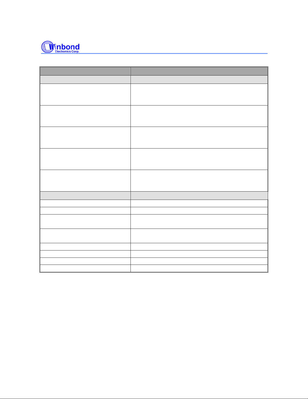
Table 4.1 W90P710 Pins Assignment (Continued)
NAME 176-PIN LQFP
LCDC ( 12 pins )
VD[7:0] /
GPIO [41:34]/
KPCOL[7:0]
HSYNC /
GPIO [33]/
KPROW[3]
VSYNC /
GPIO [32]/
KPROW[2]
VDEN /
GPIO [31]/
KPROW[1]
VCLK /
GPIO [30]/
KPROW[0]
Power/Ground ( 36 pins )
VDD18 21,63,109,160
VSS18 22,38,64,105,157
VDD33
VSS33
USBVDD 1,8
USBVSS 4,5
PLLVDD18 39,42
PLLVSS18 40,41
27-34
26
25
24
23
9,35,54,69,85,100,
120,127,139,165
16,36,51,73,80,94,
114,126,141,171
Publication Release Date: September 19, 2006
- 19 - Revision B2
Page 20
W90P710CD/W90P710CDG
5. PIN DESCRIPTION
Table 5.1 W90P710 Pins Description
PIN NAME IO TYPE DESCRIPTION
Clock & Reset
EXTAL (15M) I 15MHz External Clock / Crystal Input
XTAL (15M) O 15MHz Crystal Output
EXTAL32(32.768
K)
XTAL32(32.768K) O 32768Hz Crystal Output(for RTC)
nRESET IS System Reset, active-low
JTAG Interface
TCK IDS JTAG Test Clock, internal pull-down with 58K ohm
TMS IUS JTAG Test Mode Select, internal pull-up with 70K ohm
TDI IUS JTAG Test Data in, internal pull-up with 70K ohm
TDO O JTAG Test Data out
nTRST IUS JTAG Reset, active-low, internal pull-up with 70K ohm
External Bus Interface
A [21:18] O Address Bus (MSB) of external memory and IO devices.
A [17:0] IOS Address Bus of external memory and IO devices.
D [31:16] /
VD[23:8] /
GPIO [67:52]
D [15:0] / IOU Data Bus (LSB) of external memory and IO device.
nWBE [3:0] /
SDQM [3:0] /
GPIO[69:68]
nSCS [1:0] O SDRAM chip select for two external banks, active-low.
nSRAS O Row Address Strobe for SDRAM, active-low.
nSCAS O Column Address Strobe for SDRAM, active-low.
nSWE O SDRAM Write Enable, active-low
MCKE O SDRAM Clock Enable, active-high
MCLK O System Master Clock Out, SDRAM clock, output with slew-rate control
nWAIT /
GPIO[70] /
nIRQ5
nBTCS O ROM/Flash Chip Select, active-low.
nECS [3:0] O External I/O Chip Select, active-low.
nOE O ROM/Flash, External Memory Output Enable, active-low.
I 32768Hz External Clock / Crystal Input(for RTC)
Data Bus (MSB) of external memory and IO device, internal pull-up with 70K
IOU
IOU
IOU
ohm.
General Programmable In/Out Port GPIO[67:52].
Write Byte Enable for specific device (nECS [3:0]).
Data Bus Mask signal for SDRAM (nSCS [1:0]), active-low.
General Programmable In/Out Port [69:68]
External Wait, active-low.
This pin indicates that the external devices need more active cycle during
access operation.
General Programmable In/Out Port GPIO[70]. If memory and IO devices in EBI
do not need wait request, it can be configured as GPIO[7] or nIRQ5
- 20 -
Page 21

Table 5.1 W90P710 Pins Description (Continued)
Pin Name
Ethernet Interface
PHY_MDC /
GPIO [51] /
KPROW[1] /
VD[17]
PHY_MDIO /
GPIO [50] /
KPROW[0] /
VD[16]
PHY_TXD [1:0] /
GPIO [49:48] /
KPCOL[7:6] /
VD[15]
PHY_TXEN /
GPIO [47] /
KPCOL[5] /
VD[14:13]
PHY_REFCLK /
GPIO [46] /
KPCOL[4] /
VD[12]
PHY_RXD [1:0] /
GPIO [45:44] /
KPCOL[3:2] /
VD[11:10]
PHY_CRSDV /
GPIO [43] /
KPCOL[1] /
VD[9]
PHY_RXERR /
GPIO [42] /
KPCOL[0] /
VD[8]
IO
Type
IOU
IO
IOU
IOU
IOS
IOS
IOS
IOS
Description
RMII Management Data Clock for Ethernet. It is the reference clock of MDIO.
Each MDIO data will be latched at the rising edge of MDC clock.
General Programmable In/Out Port [51]
Keypad ROW[1] scan output.
LCD Pixel Data Output[17]
RMII Management Data I/O for Ethernet. It is used to transfer RMII control and
status information between PHY and MAC.
General Programmable In/Out Port [51]
Keypad ROW[0] scan output.
LCD Pixel Data Output[16]
2-bit Transmit Data bus for Ethernet.
General programmable In/Out Port [49:48]
Keypad Column input [7:6], active low
LCD Pixel Data Output[15].
PHY_TXEN shall be asserted synchronously with the first 2-bit of the preamble
and shall remain asserted while all di-bits to be transmitted are presented. Of
course, it is synchronized with PHY_REFCLK.
General Programmable In/Out Port [47]
Keypad column input [5], active low
LCD Pixel Data Output[14:13]
Reference Clock. The clock shall be 50MHz +/- 50 ppm with minimum 35%
duty cycle at high or low state.
General Programmable In/Out port [46]
Keypad column input [4], active low
LCD Pixel Data Output[12]
2-bit Receive Data bus for Ethernet.
General Programmable In/Out Port [45:44]
Keypad column input [3:2], active low
LCD Pixel Data Output[11:10].
Carrier Sense / Receive Data Valid for Ethernet. The PHY_CRSDV shall be
asserted by PHY when the receive medium is non-idle. Loss of carrier shall
result in the de-assertion of PHY_CRSDV synchronous to the cycle of
PHY_REFCLK, and only on 2-bit receive data boundaries.
General Programmable In/Out port [43]
Keypad column input [1], active low
LCD Pixel Data Output[9]
Receive Data Error for Ethernet. It indicates a data error detected by PHY.The
assertion should be lasted for longer than a period of PHY_REFCLK. When
PHY_RXERR is asserted, the MAC will report a CRC error.
General programmable In/Out port [42]
Keypad column input [0], active low
LCD Pixel Data Output[8]
W90P710CD/W90P710CDG
.
.
.
.
.
.
Publication Release Date: September 19, 2006
- 21 - Revision B2
Page 22
W90P710CD/W90P710CDG
Table 5.1 W90P710 Pins Description (Continued)
Pin Name
AC97/I2S/PWM/UART3
AC97_nRESET /
I2S_MCLK /
GPIO [0] /
nIRQ4 /
USB_PWREN
AC97_DATAI /
I2S_DATAI /
PWM [0] /
DTR4 /
GPIO [1]
AC97_DATAO /
I2S_DATAO /
PWM [1] /
DSR4 /
GPIO [2]
AC97_SYNC /
I2S_LRCLK /
PWM [2] /
TXD4 /
GPIO [3]
AC97_BITCLK /
I2S_BITCLK /
PWM [3] /
RXD4 /
GPIO [4]
USB Interface
DP0 IO Differential Positive USB IO signal
DN0 IO Differential Negative USB IO signal
DP1 IO Differential Positive USB IO signal
DN1 IO Differential Negative USB IO signal
Miscellaneous
nIRQ [3:2] /
GPIO [19:18]
nIRQ [1:0] /
GPIO [17:16]
USB_OVRCUR
nWDOG /
GPIO [15] /
USB_PWREN
RTCVDD P RTC independent battery power (1.8V)
IO
Type
IOU
IOU
IOU
IOU
IOS
IOU
IOU
IOU
Description
AC97 CODEC Host Interface RESET Output.
I2S CODEC Host Interface System Clock Output.
General Purpose In/Out port [0]
External interrupt request.
USB host power enable output
AC97 CODEC Host Interface Data Input.
I2S CODEC Host Interface Data Input.
PWM Channel 0 Output.
Data Terminal Ready for UART4.
General Purpose In /Out port [1]
AC97 CODEC Host Interface Data Output.
I2S CODEC Host Interface Data Output.
PWM Channel 1 Output.
Data Set Ready for UART4.
General Purpose In/Out port [2]
AC97 CODEC Host Interface Synchronous Pulse Output.
I2S CODEC Host Interface Left/Right Channel Select Clock.
PWM Channel 2 Output.
Transmit Data for UART4.
General Purpose In/Out port [3]
AC97 CODEC Host Interface Bit Clock Input.
I2S CODEC Host Interface Bit Clock.
PWM Channel 3 Output.
Receive Data for UART4.
General Purpose In/Out port [4].
External Interrupt Request
General Purpose I/O.
External Interrupt Request
General Purpose I/O
nIRQ1 is used as USB host over-current detection input
Watchdog Timer Timeout Flag and Keypad 3-keys reset output, active low
General Purpose In/output
USB host power switch enable output
- 22 -
Page 23
Table 5.1 W90P710 Pins Description (Continued)
Pin Name
I2C/USI(Microwire/SPI)
SCL0 /
SFRM /
Timer0 /
GPIO [11]
SDA0 /
SSPTXD /
Timer1 /
GPIO [12]
SCL1 /
SCLK /
GPIO [13]
KPROW[3]
SDA1 /
SSPRXD /
GPIO [14] /
KPROW[2]
UART0/UART1/UART2
TXD0 /
GPIO [5]
RXD0 /
GPIO [6]
TXD1 /
GPIO [7]
RXD1 /
GPIO [8]
CTS1/
TXD2(IrDA) /
PS2_CLK /
GPIO [9]
RTS1/
RXD2(IrDA) /
PS2_DATA /
GPIO [10]
SCHI/SD/XDMA
SC0_DAT/
SD_CMD /
GPIO [29] /
VD[17]
SC0_CLK /
SD_CLK /
GPIO [28] /
VD[16]
IO
Type
IOU
IOU
IOU
IDU
IOU
IOU
IOU
IOU
IOU
IOU
IOU
IO
Description
I2C Serial Clock Line 0.
USI Serial Frame.
Timer0 time out output.
General Purpose In/Out port [11].
I2C Serial Data Line 0
USI Serial Transmit Data
Timer1 time out output
General Purpose In/Out port [12]
I2C Serial Clock Line 1
USI Serial Clock
General Purpose In/Out port [13]
Keypad row scan output [3]
I2C Serial Data Line 1
USI Serial Receive Data
General Purpose In/Out port [14]
Keypad scan output [2]
UART0 Transmit Data.
General Purpose In/Out [5]
UART0 Receive Data.
General Purpose In/Out [6]
UART1 Transmit Data.
General Purpose In/Out [7]
UART1 Receive Data.
General Purpose In/Out [8]
UART1 Clear To Send for Bluetooth application
UART2 Transmit Data supporting SIR IrDA.
PS2 Interface Clock Input/Output
General Purpose In/Out [9]
UART1 Request To Send for Bluetooth application
UART2 Receive Data supporting SIR IrDA.
PS2 Interface Bi-Directional Data Line.
General Purpose In/Out [10]
Smart Card I/O Contact to Card 0.
SD Mode – Command/Response;
General Purpose In/Out [29]
LCD Pixel Data Output[17]
Smart Card Clock Output to Card 0.
SD Mode – Clock;
General Purpose In/Out [28]
LCD Pixel Data Output[16].
W90P710CD/W90P710CDG
.
Publication Release Date: September 19, 2006
- 23 - Revision B2
Page 24

Table 5.1 W90P710 Pins Description (Continued)
Pin Name
SCHI/SD/XDMA
SC0_RST /
SD_DAT0 /
GPIO [27] /
VD[15]
SC0_PRES /
SD_DAT1 /
GPIO [26]
VD[14]
SC0_nPWR /
SD_DAT2 /
GPIO [25] /
VD[13]
SC1_DAT /
SD_DAT3 /
GPIO [24] /
VD[12]
SC1_CLK /
GPIO [23] /
VD[11]
SC1_RST /
SD_CD /
GPIO [22] /
VD[10]
SC1_PRES /
nXDREQ /
GPIO [21] /
VD[9]
SC1_nPWR /
nXDACK /
GPIO [20] /
VD[8]
LCD Interface
VD [7:0] /
GPIO [41:34]/
KPCOL[7:0]
HSYNC /
GPIO [33]/
KPROW[3]
VSYNC /
GPIO [32]/
KPROW[2]
VDEN /
GPIO [31]/
KPROW[1]
IO
Type
IO
IO
IO
IO
IO
IO
IO
IO
IOU
IOU
IOU
IOU
Description
Smart Card Reset Output to Card 0.
SD Mode – Data Line Bit 0;
General Purpose In/Out [27]
LCD Pixel Data Output[15]
Smart Card 0 Presence Contact Input.
SD Mode – Data Line Bit 1.
General Purpose In/Out [26]
LCD Pixel Data Output[14]
Smart Card 0 Power FET Control Signal Output.
SD Mode – Data Line Bit 2.
General Purpose In/Out [25]
LCD Pixel Data Output[13].
Smart Card I/O Contact to Card 1.
SD Mode – Data Line Bit 3;
General Purpose In/Out [24]
LCD Pixel Data Output[12]
Smart Card Clock Output to Card 1.
General Purpose In/Out [23]
LCD Pixel Data Output[11]
Smart Card Reset Output to Card 1.
SD Mode – Card Detect.
General Purpose In/Out [22]
LCD Pixel Data Output[10]
Smart Card 1 Presence Contact Input.
External DMA Request.
General Purpose In/Out [21]
LCD Pixel Data Output[9]
Smart Card 1 Power FET Control Signal Output.
External DMA Acknowledgement.
General Purpose In/Out [20]
LCD Pixel Data Output[8]
LCD Pixel Data Output [7:0].
General Purpose In/Out [41:34]
Keypad Column input [7:0], active low
Horizontal Sync
General Purpose In/Out [33]
Keypad ROW[3] scan output.
Vertical Sync
General Purpose In/Out [32]
Keypad ROW[2] scan output.
Data Enable or Display Control Signal.
General Purpose In/Out [31]
Keypad ROW[1] scan output.
W90P710CD/W90P710CDG
.
.]
.
.
.
.
.
- 24 -
Page 25
Table 5.1 W90P710 Pins Description (Continued)
Pin Name
Power/Ground
VDD18 P Core Logic power (1.8V)
VSS18 G Core Logic ground (0V)
VDD33 P IO Buffer power (3.3V)
VSS33 G IO Buffer ground (0V)
USBVDD P USB power (3.3V)
USBVSS G USB ground (0V)
DVDD18 P PLL Digital power (1.8V)
DVSS18 G PLL Digital ground (0V)
AVDD18 P PLL Analog power (1.8V)
AVSS18 G PLL Analog ground (0V)
IO
Type
Description
W90P710CD/W90P710CDG
Publication Release Date: September 19, 2006
- 25 - Revision B2
Page 26
W90P710CD/W90P710CDG
Table 5.2 W90P710 176-pin LQFP Multi-function List
PIN
NO.
1 USB1VDD
2 DP1
3 DN1
4 USB1VSS
5 USB0VSS
6 DN0
7 DP0
8 USB0VDD
9 VDD33
10 GPIO[5]
11 GPIO[6]
12 GPIO[7]
13 GPIO[8]
14 GPIO[9]
DEFAULT FUNCTION0 FUNCTION1 FUNCTION2 FUNCTION3
USB1.1 Host/Device Interface
USB1VDD - - -
DP1 - - -
DN1 - - -
USB1VSS - - -
USB0VSS - - -
DN0 - - -
DP0 - - -
USB0VDD - - -
VDD33 - - -
UART[2:0]/PS2 Interface
GPIO[5] UART_TXD0 - -
GPIO[6] UART_RXD0 - -
GPIO[7] UART_TXD1 - -
GPIO[8] UART_RXD1 - -
GPIO[9] UART_TXD2 UART_CTS1 PS2_CLK
15 GPIO[10]
16 VSS33
17 GPIO[11]
18 GPIO[12]
19 GPIO[13]
20 GPIO[14]
21 VDD18
22 VSS18
23 GPIO[30]
24 GPIO[31]
25 GPIO[32]
26 GPIO[33]
27 GPIO[41]
GPIO[10] UART_RXD2 UART_RTS1 PS2_DATA
VSS33 - - -
I2C/USI Interface
GPIO[11] I2C_SCL0 SSP_FRAM TIMER0
GPIO[12] I2C_SDA0 SSP_TXD TIMER1
GPIO[13] I2C_SCL1 SSP_RXD KPROW[2]
GPIO[14] I2C_SDA1 SSP_SCLK KPROW[3]
VDD18 - - -
VSS18 - - -
LCD /KeyPad Interface
GPIO[30] LCD_VCLK KPROW[0] -
GPIO[31] LCD_VDEN KPROW[1] -
GPIO[32] LCD_VSYNC KPROW[2] -
GPIO[33] LCD_HSYNC KPROW[3] -
GPIO[41] LCD_VD[7] KPCOL[7] -
- 26 -
Page 27
Table 5.2 W90P710 176-pin LQFP Multi-function List (Continued)
W90P710CD/W90P710CDG
PIN
NO.
28 GPIO[40]
29 GPIO[39]
30 GPIO[38]
31 GPIO[37]
32 GPIO[36]
33 GPIO[35]
34 GPIO[34]
35 VDD33
36 VSS33
37 nRESET
38 VSS33
39 PLL0_VDD18
DEFAULT FUNCTION0 FUNCTION1 FUNCTION2 FUNCTION3
LCD /KeyPad Interface
GPIO[40] LCD_VD[6] KPCOL[6] -
GPIO[39] LCD_VD[5] KPCOL[5] -
GPIO[38] LCD_VD[4] KPCOL[4] -
GPIO[37] LCD_VD[3] KPCOL[3] -
GPIO[36] LCD_VD[2] KPCOL[2] -
GPIO[35] LCD_VD[1] KPCOL[1] -
GPIO[34] LCD_VD[0] KPCOL[0] -
VDD33 - - -
VSS33 - - -
System Reset
nRESET - - -
VSS33 - - -
PLL Power/Ground
PLL0_VDD18 - - -
40 PLL0_VSS18
41 PLL1_VSS18
42 PLL1_VDD18
43 GPIO[16]
44 GPIO[17]
45 TMS
46 TDI
47 TDO
48 TCK
49 nTRST
50 GPIO[15]
51 VSS33
PLL0_VSS18 - - -
PLL1_VSS18 - - -
PLL1_VDD18 - - -
External IRQ[1:0]/USB Over Current
GPIO[16] nIRQ[0] - -
GPIO[17] nIRQ[1] USB_OVRCUR -
JTAG Interface
TMS - - -
TDI - - -
TDO - - -
TCK - - -
nTRST - - -
WatchDog/USB Power Enable
GPIO[15] nWDOG USB_PWREN -
VSS33 - - -
Publication Release Date: September 19, 2006
- 27 - Revision B2
Page 28
Table 5.2 W90P710 176-pin LQFP Multi-function List (Continued)
W90P710CD/W90P710CDG
PIN
NO.
52 EXTAL(15M)
53 XTAL(15M)
54 VDD33
55 RTCVDD18
56 XTAL32 (32K)
57 EXTAL32 (32K)
58 GPIO[0]
59 GPIO[1]
60 GPIO[2]
61 GPIO[3]
62 GPIO[4]
63 VDD18
DEFAULT FUNCTION0 FUNCTION1 FUNCTION2 FUNCTION3
System/RTC Clock
EXTAL(15M) - - -
XTAL(15M) - - -
VDD33 - - -
RTCVDD18 - - -
XTAL32 (32K) - - -
EXTAL32 (32K) - - -
AC97/I2S/PWM/UART3 Interface
GPIO[0]
GPIO[1]
GPIO[2]
GPIO[3]
GPIO[4]
VDD18
AC97_nRESET
AC97_DATAI
AC97_DATAO
AC97_SYNC
AC97_BITCLK
-
IRQ4 USB_PWREN
PWM0 UART_DTR3
PWM1 UART_DSR3
PWM2 UART_TXD3
PWM3 UART_RXD3
- -
64 VSS18
SmartCard/SD/USB Power/XDMAREQ/LCD Interace
65 GPIO[29]
66 GPIO[28]
67 GPIO[27]
68 GPIO[26]
69 VDD33
70 GPIO[25]
71 GPIO[24]
72 GPIO[23]
73 VSS33
74 GPIO[22]
75 GPIO[21]
76 GPIO[20]
VSS18 - - -
GPIO[29] SD_CMD SC0_IO LCD_VD[17]
GPIO[28] SD_CLK SC0_CLK LCD_VD[16]
GPIO[27] SD_DAT[0] SC0_RST LCD_VD[15]
GPIO[26] SD_DAT[1] SC0_PRES LCD_VD[14]
VDD33
GPIO[25] SD_DAT[2] SC0_PWR LCD_VD[13]
GPIO[24] SD_DAT[3] SC1_IO LCD_VD[12]
GPIO[23] USBPWREN SC1_CLK LCD_VD[11]
VSS33
GPIO[22] SD_CD SC1_RST LCD_VD[10]
GPIO[21] nXQREQ SC1_PRES LCD_VD[9]
GPIO[20] nXDACK SC1_PWR LCD_VD[8]
- 28 -
Page 29
Table 5.2 W90P710 176-pin LQFP Multi-function List (Continued)
W90P710CD/W90P710CDG
PIN
NO.
77 GPIO[42]
78 GPIO[43]
79 GPIO[44]
80 VSS33
81 GPIO[45]
82 GPIO[46]
83 GPIO[47]
84 GPIO[48]
85 VDD33
86 GPIO[49]
87 GPIO[50]
88 GPIO[51]
89 A[0]
DEFAULT FUNCTION0 FUNCTION1 FUNCTION2 FUNCTION3
Ethernet RMII/KeyPad Interface
GPIO[42] PHY_RXERR KPCOL[0] LCD_VD[8]
GPIO[43] PHY_CRSDV KPCOL[1] LCD_VD[9]
GPIO[44] PHY_RXD[0] KPCOL[2] LCD_VD[10]
VSS33 - - -
GPIO[45] PHY_RXD[1] KPCOL[3] LCD_VD[11]
GPIO[46] PHY_REFCLK KPCOL[4] LCD_VD[12]
GPIO[47] PHY_TXEN KPCOL[5] LCD_VD[13]
GPIO[48] PHY_TXD[0] KPCOL[6] LCD_VD[14]
VDD33 - -
GPIO[49] PHY_TXD[1] KPCOL[7] LCD_VD[15]
GPIO[50] PHY_MDIO KPROW[0] LCD_VD[16]
GPIO[51] PHY_MDC KPROW[1] LCD_VD[17]
Memory Address/Data/Control
A[0] - - -
90 A[1]
91 A[2]
92 A[3]
93 A[4]
94 VSS33
95 A[5]
96 A[6]
97 A[7]
98 A[8]
99 A[9]
100 VDD33
101 A[10]
102 A[11]
103 A[12]
104 A[13]
A[1] - - -
A[2] - - -
A[3] - - -
A[4] - - -
VSS33 - - -
A[5] - - -
A[6] - - -
A[7] - - -
A[8] - - -
A[9] - - -
VDD33 - - -
A[10] - - -
A[11] - - -
A[12] - - -
A[13] - - -
Publication Release Date: September 19, 2006
- 29 - Revision B2
Page 30
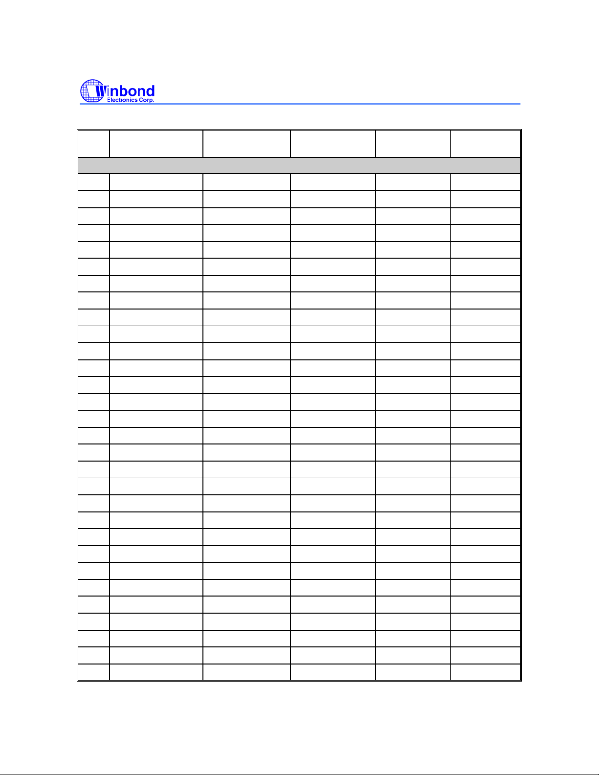
Table 5.2 W90P710 176-pin LQFP Multi-function List (Continued)
W90P710CD/W90P710CDG
PIN
NO.
105 VSS18
106 A[14]
107 A[15]
108 A[16]
109 VDD18
110 A[17]
111 A[18]
112 A[19]
113 A[20]
114 VSS33
115 A[21]
116 D[31]
117 D[30]
118 D[29]
119 D[28]
DEFAULT FUNCTION0 FUNCTION1 FUNCTION2 FUNCTION3
Memory Address/Data/Control
VSS18 - - -
A[14] - - -
A[15] - - -
A[16] - - -
VDD18 - - -
A[17] - - -
A[18] - - -
A[19] - - -
A[20] - - -
VSS33 - - -
A[21] - - -
GPIO[67] D[31] LCD_VD[23] -
GPIO[66] D[30] LCD_VD[22] -
GPIO[65] D[29] LCD_VD[21] -
GPIO[64] D[28] LCD_VD[20] -
120 VDD33
121 D[27]
122 D[26]
123 D[25]
124 D[24]
125 nECS[3]
126 VSS33
127 VDD33
128 nECS[2]
129 nECS[1]
130 nECS[0]
131 nOE
132 nWAIT
133 nBTCS
134 MCKE
VDD33 - - -
GPIO[63] D[27] LCD_VD[19] -
GPIO[62] D[26] LCD_VD[18] -
GPIO[61] D[25] LCD_VD[17] -
GPIO[60] D[24] LCD_VD[16] -
nECS[3] - - -
VSS33 - - -
VDD33 - - -
nECS[2] - - -
nECS[1] - - -
nECS[0] - - -
nOE - - -
GPIO[71] nWAIT IRQ5 -
nBTCS - - -
MCKE - - -
- 30 -
Page 31
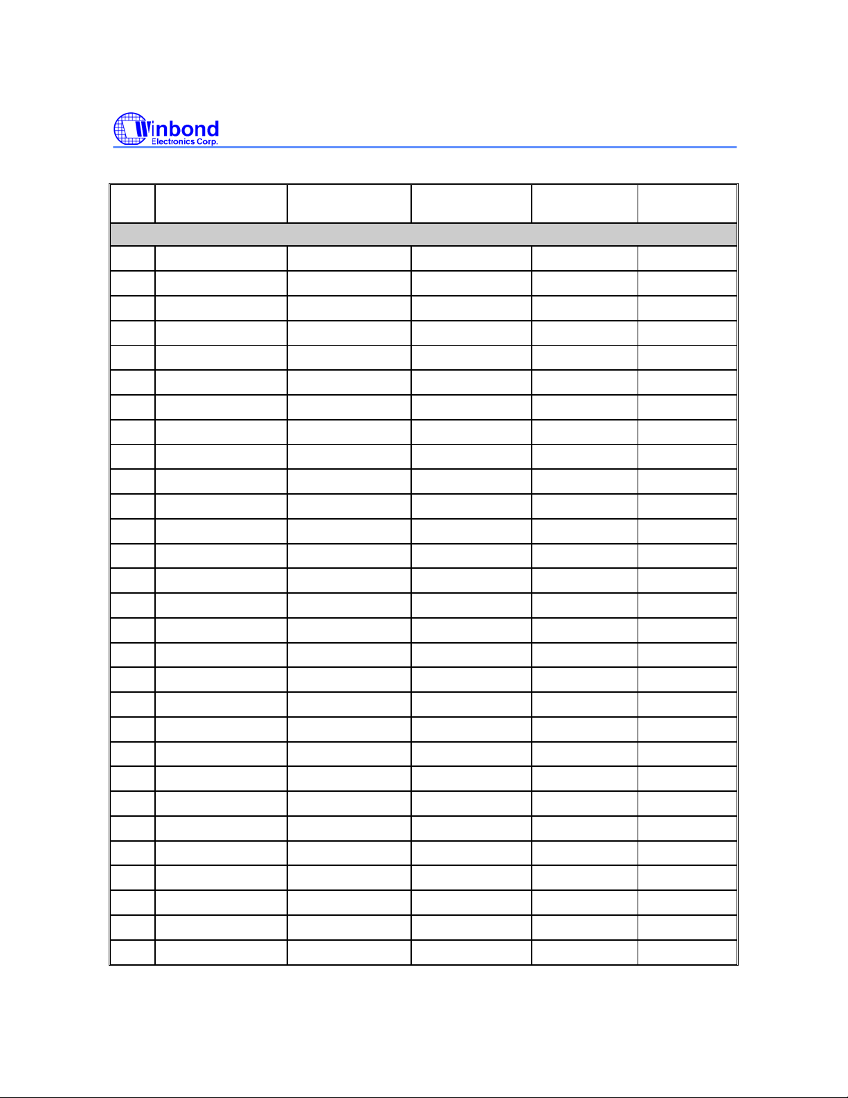
Table 5.2 W90P710 176-pin LQFP Multi-function List (Continued)
W90P710CD/W90P710CDG
PIN
NO.
135 nSCS[0]
136 nSCS[1]
137 nSRAS
138 nSCAS
139 VDD33
140 MCLK
141 VSS33
142 nWE
143 nWBE_SDQM[0]
144 nWBE_SDQM[1]
145 nWBE_SDQM[2]
146 nWBE_SDQM[3]
147 GPIO[18]
148 GPIO[19]
DEFAULT FUNCTION0 FUNCTION1 FUNCTION2 FUNCTION3
Memory Address/Data/Control
nSCS[0] - - -
nSCS[1] - - -
nSRAS - - -
nSCAS - - -
VDD33 - - -
MCLK - - -
VSS33 - - -
nWE - - -
nWBE_SDQM[0] - - -
nWBE_SDQM[1] - - -
GPIO[69] nWBE_SDQM[2] - -
GPIO[68] nWBE_SDQM[3] - -
GPIO[18] nIRQ[2] - -
GPIO[19] nIRQ[3] - -
149 GPIO[59]
150 D[22]
151 D[21]
152 D[20]
152 D[20]
153 D[19]
154 D[18]
155 D[17]
156 D[16]
157 VSS18
158 D[15]
159 D[14]
160 VDD18
161 D[13]
162 D[12]
GPIO[59] D[23] LCD_VD[15] -
GPIO[58] D[22] LCD_VD[14] -
GPIO[57] D[21] LCD_VD[13] -
GPIO[56] D[20] LCD_VD[12] -
GPIO[56] D[20] LCD_VD[12] -
GPIO[55] D[19] LCD_VD[11] -
GPIO[54] D[18] LCD_VD[10] -
GPIO[53] D[17] LCD_VD[9] -
GPIO[52] D[16] LCD_VD[8] -
VSS18 - - -
D[15] - - -
D[14] - - -
VDD18 - - -
D[13] - - -
D[12] - - -
Publication Release Date: September 19, 2006
- 31 - Revision B2
Page 32
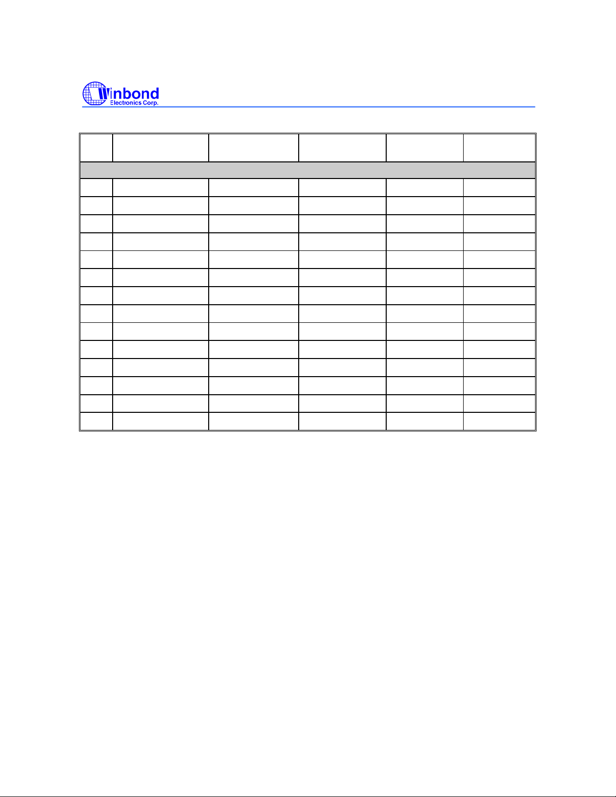
Table 5.2 W90P710 176-pin LQFP Multi-function List (Continued)
W90P710CD/W90P710CDG
PIN
NO.
163 D[11]
164 D[10]
165 VDD33
166 D[9]
167 D[8]
168 D[7]
169 D[6]
170 D[5]
171 VSS33
172 D[4]
173 D[3]
174 D[2]
175 D[1]
176 D[0]
DEFAULT FUNCTION0 FUNCTION1 FUNCTION2 FUNCTION3
Memory Address/Data/Control
D[11] - - -
D[10] - - -
VDD33 - - -
D[9] - - -
D[8] - - -
D[7] - - -
D[6] - - -
D[5] - - -
VSS33 - - -
D[4] - - -
D[3] - - -
D[2] - - -
D[1] - - -
D[0] - - -
- 32 -
Page 33
W90P710CD/W90P710CDG
6. FUNCTIONAL DESCRIPTION
6.1 ARM7TDMI CPU CORE
The ARM7TDMI CPU core is a member of the Advanced RISC Machines (ARM) family of generalpurpose 32-bit microprocessors, which offer high performance for very low power consumption. The
architecture is based on Reduced Instruction Set Computer (RISC) principles, and the instruction set and
related decode mechanism are much simpler than those of micro-programmed Complex Instruction Set
Computers. Pipelining is employed so that all parts of the processing and memory systems can operate
continuously. The high instruction throughput and impressive real-time interrupt response are the major
benefits.
The ARM7TDMI CPU core has two instruction sets:
(1) The standard 32-bit ARM set
(2) A 16-bit THUMB set
The THUMB set’s 16-bit instruction length allows it to approach twice the density of standard ARM core
while retaining most of the ARM’s performance advantage over a traditional 16-bit processor using 16-bit
registers. THUMB instructions operate with the standard ARM register configuration, allowing excellent
interoperability between ARM and THUMB states. Each 16-bit THUMB instruction has a corresponding
32-bit ARM instruction with the same effect on the processor model.
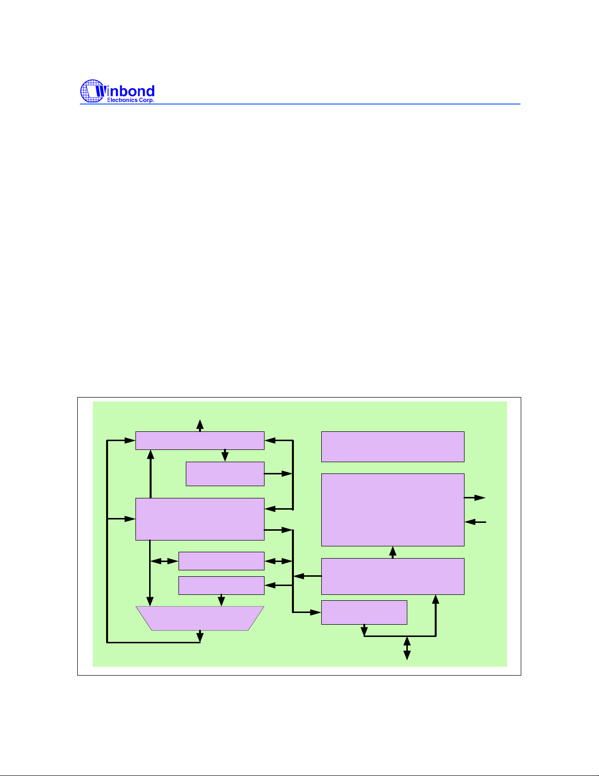
ARM7TDMI CPU core has 31 x 32-bit registers. At any one time, 16 sets are visible; the other registers
are used to speed up exception processing. All the register specified in ARM instructions can address
any of the 16 registers. The CPU also supports 5 types of exception, such as two levels of interrupt,
memory aborts, attempted execution of an undefined instruction and software interrupts.
A[31:0]
Address Register
PC Bus
Register Bank
(31 x 32-bit registers)
(6 status registers)
ALU Bus
A Bus
32-bit ALU
Address
Incrementer
32 x8 Multiplier
Barrel Shifter
Incrementer Bus
B Bus
Scan Control
Instruction Decoder
Control Logic
Instruction Pipeline
Read Data Register
Thumb Instruction Decoder
Writer Data
Register
D[31:0]
Fig 6.1 ARM7TDMI CPU Core Block Diagram
Publication Release Date: September 19, 2006
- 33 - Revision B2
Page 34

W90P710CD/W90P710CDG
6.2 System Manager
6.2.1 Overview
The W90P710 System Manager has the following functions.
y System memory map
y Data bus connection with external memory
y Product identifier register
y Bus arbitration
y PLL module
y Clock select and power saving control register
y Power-On setting
6.2.2 System Memory Map
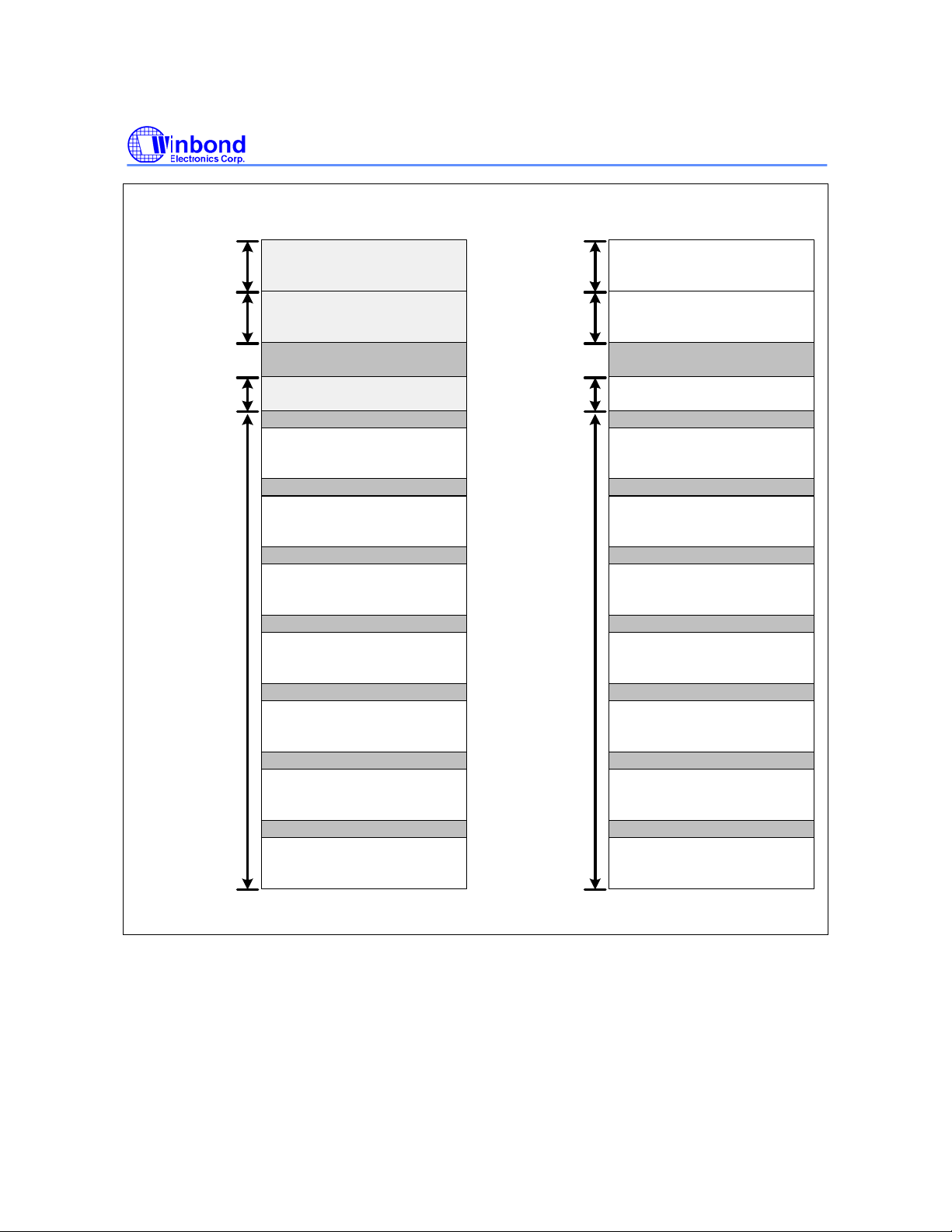
W90P710 provides 2G bytes cacheable address space and the other 2G bytes are non-cacheable. The
On-Chip Peripherals bank is on 1M bytes top of the space (0xFFF0_0000 – 0xFFFF_FFFF) and the OnChip RAM bank’s start address is 0xFFE0.0000, the other banks can be located anywhere (cacheable
space: 0x0000_0000 ~ 0x7FDF_FFFF if Cache ON; non-cacheable space: 0x8000_0000 ~
0xFFDF_FFFF).
The size and location of each bank is determined by the register settings for “current bank base address
pointer” and “current bank size”. Please note that when setting the bank control registers, the address
boundaries of consecutive banks must not overlap.
Except On-Chip Peripherals and On-Chip RAM, the start address of each memory bank is not fixed. You
can use bank control registers to assign a specific bank start address by setting the bank’s base pointer
(13 bits). The address resolution is 256K bytes. The bank’s start address is defined as “base pointer <<
18” and the bank’s size is “current bank size”.
In the event of an access requested to an address outside any programmed bank size, an abort signal is
generated. The maximum accessible memory size of each external IO bank is 16M bytes (by word
format), and 64M bytes on each SDRAM bank.
- 34 -
Page 35
0x7FFF_FFFF
512KB
(Fixed)
0x7FF8.0000
512KB
(Fixed)
0x7FF0_0000
W90P710CD/W90P710CDG
Cacheable space Non-Cacheable space
RESERVED
RESERVED
RESERVED
0xFFFF_FFFF
512KB
(Fixed)
0xFFF8_0000
512KB
(Fixed)
0xFFF0_0000
On-Chip APB
Peripherals
On-Chip AHB
Peripherals
RESERVED
8KB
0x7FE0_0000
EBI Space
RESERVED
External I/O Bank 3
256KB - 16MB
External I/O Bank 2
256KB - 16MB
External I/O Bank 1
256KB - 16MB
External I/O Bank 0
256KB - 16MB
SDRAM Bank 1
2MB - 64MB
SDRAM Bank 0
2MB - 64MB
8KB
0xFFE0_0000
EBI Space
On-Chip RAM
4KB,4KB
External I/O Bank 3
256KB - 16MB
External I/O Bank 2
256KB - 16MB
External I/O Bank 1
256KB - 16MB
External I/O Bank 0
256KB - 16MB
SDRAM Bank 1
2MB - 64MB
SDRAM Bank 0
2MB - 64MB
0x0000_0000
ROM/FLASH
256KB - 16MB
Fig6.2.1 System Memory Map
ROM/FLASH
256KB - 32MB
0x8000_0000
Publication Release Date: September 19, 2006
- 35 - Revision B2
Page 36

W90P710CD/W90P710CDG
Table 6.2.1 On-Chip Peripherals Memory Map
BASE ADDRESS DESCRIPTION
AHB Peripherals
0xFFF0_0000 Product Identifier Register (PDID)
0xFFF0_0004 Arbitration Control Register (ARBCON)
0xFFF0_0008 PLL Control Register 0(PLLCON0)
0xFFF0_000C Clock Select Register (CLKSEL)
0xFFF0_0010 PLL Control Register 1 (PLLCON1)
0xFFF0_0014 Audio IIS Clock Control Register (I2SCKCON)
0xFFF0_0020 IRQ Wakeup Control Register (IRQWAKEUPCON)
0xFFF0_0024 IRQ Wakeup Flag Register (IRQWAKEFLAG)
0xFFF0_0028 Power Manager Control Register (PMCON)
0xFFF0_0030 USB Transceiver Control Register (USBTXRCON)
0xFFF0_1000 EBI Control Register (EBICON) Control Registers
0xFFF0_1004 ROM/FLASH (ROMCON) Control Registers
0xFFF0_1008 SDRAM bank 0 – 1 Control Registers
0xFFF0_1018 External I/O 0 – 3 Control Registers
0xFFF0_2000 Cache Controller Control Registers
0xFFF0_3000 Ethernet MAC Controller Control Registers
0xFFF0_4000 GDMA 0 – 1 Control Registers
0xFFF0_5000 USB Host Controller Control Registers
0xFFF0_6000 USB Device Controller Control Registers
0xFFF0_7000 SD Host Controller Control Registers
0xFFF0_8000 LCD Controller Control Registers
0xFFF0_9000 AC97/I2S Controller Control Registers
APB Peripherals
0xFFF8_0000 UART 0 (Tx, RX for console)
0xFFF8_0100 UART 1 (Tx, Rx, for blue-tooth)
0xFFF8_0200 UART 2 (blue-tooth CTS, RTS/ IrDA Tx, Rx)
0xFFF8_0300 UART 3 (micro-print DTR, DTS, Tx, Rx)
0xFFF8_1000 Timer 0 – 1, WDOG Timer
0xFFF8_2000 Interrupt Controller
0xFFF8_3000 GPIO
0xFFF8_4000 Real Time Clock Controller Control Registers (RTC)
0xFFF8_5000 Smart Card Host Interface Control Registers (SCHI)
0xFFF8_6000 I2C-0 Control Registers
0xFFF8_6100 I2C-1 Control Registers
0xFFF8_6200 USI Control Registers
- 36 -
Page 37
W90P710CD/W90P710CDG
Table 6.2.1 On-Chip Peripherals Memory Map (Continued)
BASE ADDRESS DESCRIPTION
APB Peripherals
0xFFF8_7000 Pulse Width Modulation (PWM) Control Registers
0xFFF8_8000 KeyPad Interface Control Register (KPI)
0xFFF8_9000 PS2 Control Registers
6.2.3 Address Bus Generation
The W90P710 address bus generation is depended on the required data bus width of each memory
bank. The data bus width is determined by DBWD bits in each bank’s control register.
The maximum accessible memory size of each external IO bank is 16M bytes.
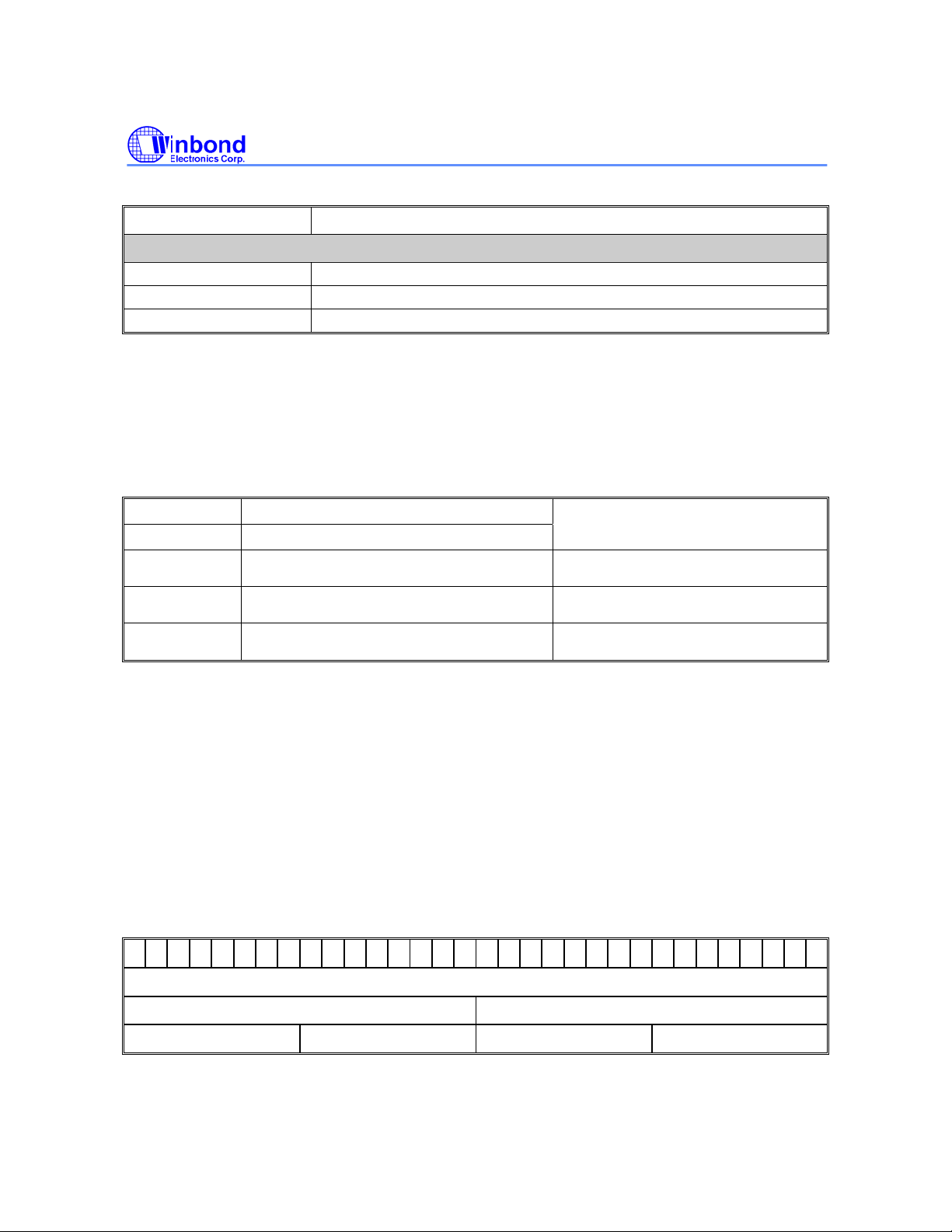
Table 6.2.2 Address Bus Generation Guidelines
DATA BUS EXTERNAL ADDRESS PINS
WIDTH A [21:0]
8-bit
16-bit
32-bit
A21 – A0
(Internal)
A22 – A1
(Internal)
A23 – A2
(Internal)
MAXIMUM ACCESSIBLE MEMORY
SIZE
4M bytes
4M half-words
4M words
6.2.4 Data Bus Connection with External Memory
6.2.4.1 Memory formats
The W90P710 can be configured as big endian or little endian mode by pull up or down the external data
bus D14 pin. If D14 is pull-up then it is a little endian mode, otherwise, it is a big endian mode.
Little endian
In little endian format, the lowest addressed byte in a word is considered the least significant byte of the
word and the highest addressed byte is the most significant. So the byte at address 0 of the memory
system connects to data lines 7 through 0.
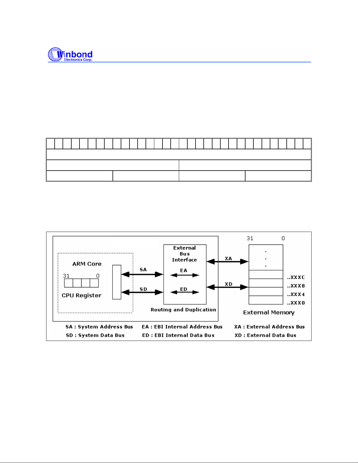
For a word aligned address A, Fig6.2.2 shows how the word at address A, the half-word at addresses A
and A+2, and the bytes at addresses A, A+1, A+2, and A+3 map on to each other when D14 pin is High.
31 30 29 28 27 26 25 24 23 22 21 20 19 18 17 16 15 14 13 12 11 10 9 8 7 6 5 4 3 2 1 0
Word at address A
Half-word at address A+2 Half-word at address A
Byte at address A+3 Byte at address A+2 Byte at address A+1 Byte at address A
Fig6.2.2 Little endian addresses of bytes and half-words within words
Publication Release Date: September 19, 2006
- 37 - Revision B2
Page 38
W90P710CD/W90P710CDG
Big endian
In Big endian format, the W90P710 stores the most significant byte of a word at the lowest numbered
byte, and the least significant byte at the highest-numbered byte. So the byte at address 0 of the memory
system connects to data lines 31 through 24.
For a word aligned address A, Fig6.2.3 shows how the word at address A, the half-word at addresses A
and A+2, and the bytes at addresses A, A+1, A+2, and A+3 map on to each other when the D14 pin is
Low.
31 30 29 28 27 26 25 24 23 22 21 20 19 18 17 16 15 14 13 12 11 10 9 8 7 6 5 4 3 2 1 0
Word at address A
Half-word at address A Half-word at address A+2
Byte at address A Byte at address A+1 Byte at address A+2 Byte at address A+3
Fig6.2.3 Big endian addresses of bytes and half-words within words
6.2.4.2 Connection of External Memory with Various Data Width
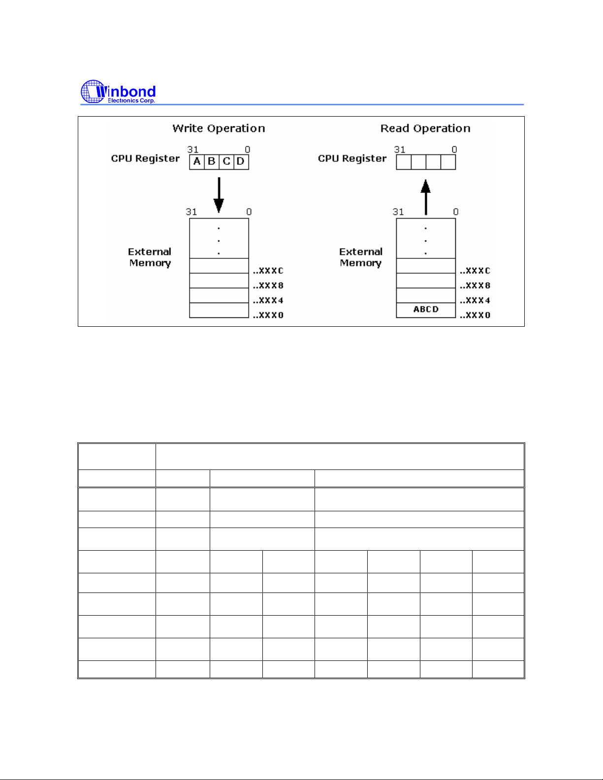
The system diagram for W90P710 connecting with the external memory is shown in Fig6.2.4. Below
tables (Table6.2.3 through Table6.2.14) show the program/data path between CPU register and the
external memory using little / big endian and word/half-word/byte access.
W90P710
Fig6.2.4 Address/Data bus connection with external memory
- 38 -
Page 39
W90P710CD/W90P710CDG
Fig6.2.5 CPU registers Read/Write with external memory
Table 6.2.3 and Table 6.2.4
Using big-endian and word access, Program/Data path between register and external memory
WA = Address whose LSB is 0,4,8,C X = Don’t care
nWBE [3-0] / SDQM [3-0] = A means active and U means inactive
Table6.2.3 Word access write operation with Big Endian
ACCESS
OPERATION
XD WIDTH WORD HALF WORD BYTE
Bit Number
CPU Reg Data
SA
Bit Number
SD
Bit Number
ED
XA
nWBE [3-0] /
SDQM [3-0]
Bit Number
XD
Bit Number
Ext. Mem Data
Timing Sequence 1st write 2nd write 1st write 2nd write 3rd write 4th write
31 0
ABCD
WA WA WA
31 0
ABCD
31 0
ABCD
WA WA WA+2 WA WA+1 WA+2 WA+3
AAAA XXAA XXAA XXXA XXXA XXXA XXXA
31 0
ABCD
31 0
ABCD
WRITE OPERATION (CPU REGISTER Î EXTERNAL MEMORY)
15 0
AB
15 0
AB
15 0
AB
31 0
ABCD
31 0
AB CD
15 0
CD
15 0
CD
15 0
CD
7 0
A
7 0
A
7 0
A
31 0
A B C D
7 0
B
7 0
B
7 0
B
31 0
ABCD
7 0
C
7 0
C
7 0
C
7 0
D
7 0
D
7 0
D
Publication Release Date: September 19, 2006
- 39 - Revision B2
Page 40
W90P710CD/W90P710CDG
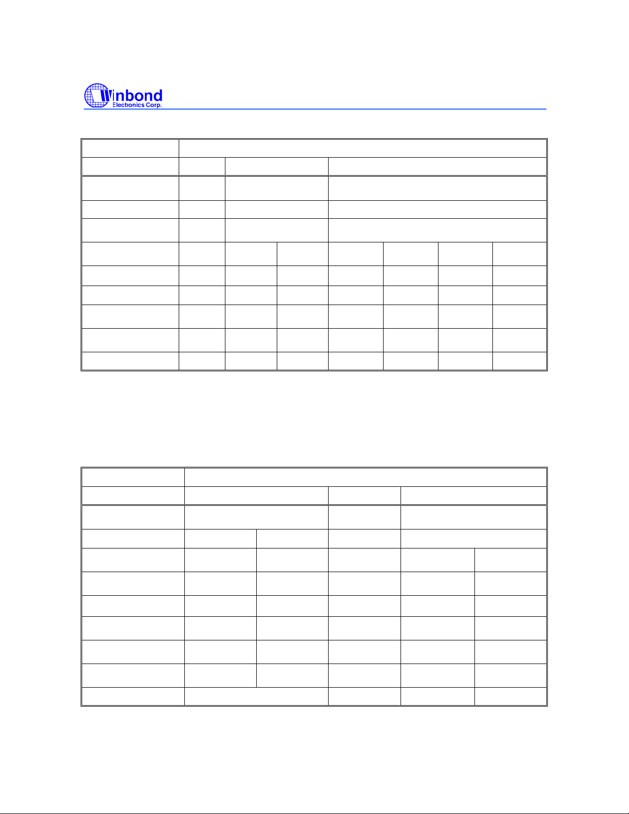
Table6.2.4 Word access read operation with Big Endian
ACCESS OPERATION READ OPERATION (CPU REGISTER Í EXTERNAL MEMORY)
XD WIDTH WORD HALF WORD BYTE
Bit Number
CPU Reg Data
SA
Bit Number
SD
Bit Number
ED
XA
31 0
ABCD
WA WA WA
31 0
ABCD
31 0
ABCD
WA WA WA+2 WA WA+1 WA+2 WA+3
31 0
CD AB
31 0
CD XX
31 0
CDAB
31 0
CD AB
31 0
D X X X
31 0
D C B A
31 0
D C X X
31 0
DCBA
31 0
D C B X
31 0
D C B A
SDQM [3-0]
Bit Number
XD
Bit Number
Ext. Mem Data
Timing Sequence 1st read 2nd read 1st read 2nd read 3rd read 4th read
AAAA XXAA XXAA XXXA XXXA XXXA XXXA
31 0
ABCD
31 0
ABCD
15 0
CD
15 0
CD
15 0
AB
15 0
AB
7 0
D
7 0
D
7 0
C
7 0
C
7 0
B
7 0
B
7 0
A
7 0
A
Table 6.2.5 and Table 6.2.6
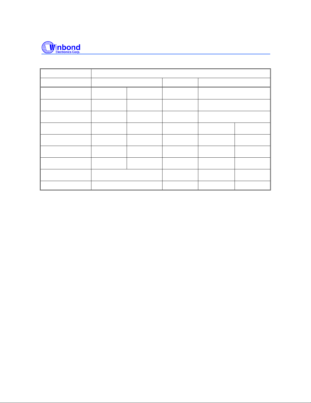
Using big-endian and half-word access, Program/Data path between register and external memory.
HA = Address whose LSB is 0,2,4,6,8,A,C,E HAL = Address whose LSB is 0,4,8,C
HAU = Address whose LSB is 2,6,A,E X = Don’t care
nWBE [3-0] / SDQM [3-0] = A means active and U means inactive
Table6.2.5 Half-word access write operation with Big Endian
ACCESS OPERATION WRITE OPERATION (CPU REGISTER Î EXTERNAL MEMORY)
XD WIDTH WORD HALF WORD BYTE
Bit Number
CPU Reg Data
SA
Bit Number
SD
Bit Number
ED
XA
nWBE [3-0] /
SDQM [3-0]
Bit Number
XD
Bit Number
Ext. Mem Data
Timing Sequence 1st write 2nd write
HAL HAU HA HA
31 0
CD CD
31 0
CD CD
HAL HAL HA HA HA+1
AAUU UUAA XXAA XXXA XXXA
31 0
CD CD
31 16
CD
31 0
ABCD
31 0
CD CD
31 0
CD CD
31 0
CD CD
15 0
CD
31 0
ABCD
31 0
CD CD
31 0
CD CD
15 0
CD
15 0
CD
31 0
CD CD
7 0
C
7 0
C
7 0
C
31 0
ABCD
31 0
CD CD
7 0
D
7 0
D
7 0
D
- 40 -
Page 41
W90P710CD/W90P710CDG
Table6.2.6 Half-word access read operation with Big Endian
ACCESS OPERATION READ OPERATION (CPU REGISTER Í EXTERNAL MEMORY)
XD WIDTH WORD HALF WORD BYTE
Bit Number
CPU Reg Data
15 0
AB
15 0
CD
15 0
CD
15 0
DC
SA
Bit Number
SD
Bit Number
ED
XA
SDQM [3-0]
Bit Number
XD
Bit Number
Ext. Mem Data
Timing Sequence 1st read 2nd read
HAL HAU HA HA
15 0
AB
15 0
AB
HAL HAL HA HA HA+1
AAUU UUAA XXAA XXXA XXXA
31 0
AB CD
31 0
ABCD
15 0
CD
15 0
CD
31 0
AB CD
15 0
CD
15 0
CD
15 0
CD
15 0
CD
15 0
DX
7 0
D
7 0
D
15 0
DC
15 0
DC
7 0
7 0
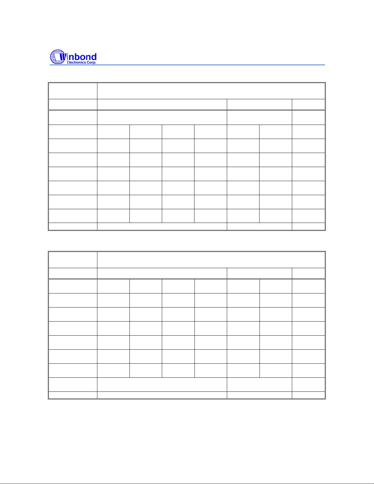
Table 6.2.7 and Table 6.2.8
Using big-endian and byte access, Program/Data path between register and external memory.
BA = Address whose LSB is 0,1,2,3,4,5,6,7,8,9,A,B,C,D,E,F
BAL = Address whose LSB is 0,2,4,6,8,A,C,E BAU = Address whose LSB is 1,3,5,7,9,B,D,F
BA0 = Address whose LSB is 0,4,8,C BA1 = Address whose LSB is 1,5,9,D
BA2 = Address whose LSB is 2,6,A,E BA3 = Address whose LSB is 3,7,B,F
C
C
Publication Release Date: September 19, 2006
- 41 - Revision B2
Page 42
W90P710CD/W90P710CDG
Table6.2.7 Byte access write operation with Big Endian
ACCESS
OPERATION
XD WIDTH WORD HALF WORD BYTE
Bit Number
CPU Reg Data
SA
Bit Number
SD
Bit Number
ED
XA
nWBE [3-0] /
SDQM [3-0]
Bit Number
XD
Bit Number
Ext. Mem Data
Timing Sequence
BA0 BA1 BA2 BA3 BAL BAU BA
31 0
D D D D
31 24
BA0 BA0 BA0 BA0 BAL BAL BA
AUUU UAUU UUAU UUUA XXAU XXUA XXXA
31 0
D X X X
31 24
WRITE OPERATION (CPU REGISTER Î EXTERNAL MEMORY)
D
D
31 0
D D D D
23 16
D
31 0
X D X X
23 16
D
31 0
ABCD
31 0
D D D D
15 8
D
31 0
X X D X
15 8
D
31 0
D D D D
7 0
D
31 0
X X X D
7 0
D
31 0
D D D D
31 0
ABCD
15 8
D
15 0
D X
15 8
D
31 0
D D D D
7 0
D
15 0
X D
7 0
D
Table6.2.8 Byte access read operation with Big Endian
ACCESS
OPERATION
XD WIDTH WORD HALF WORD BYTE
Bit Number
CPU Reg Data
7 0
A
READ OPERATION (CPU REGISTER Í EXTERNAL MEMORY)
7 0
B
7 0
C
7 0
D
7 0
C
7 0
D
31 0
ABCD
31 0
D D D D
7 0
D
7 0
D
7 0
D
7 0
D
SA
Bit Number
SD
Bit Number
ED
XA
SDQM [3-0]
Bit Number
XD
Bit Number
Ext. Mem Data
Timing Sequence
BA0 BA1 BA2 BA3 BAL BAU BA
7 0
A
7 0
A
BA0 BA0 BA0 BA0 BAL BAL BA
AUUU UAUU UUAU UUUA XXAU XXUA XXXA
31 0
ABCD
7 0
B
15 8
B
31 0
ABCD
7 0
C
23 16
C
31 0
ABCD
31 0
ABCD
7 0
D
31 24
D
31 0
ABCD
7 0
C
7 0
C
15 0
CD
15 0
CD
7 0
D
15 8
D
15 0
CD
7 0
D
7 0
D
7 0
D
7 0
D
- 42 -
Page 43
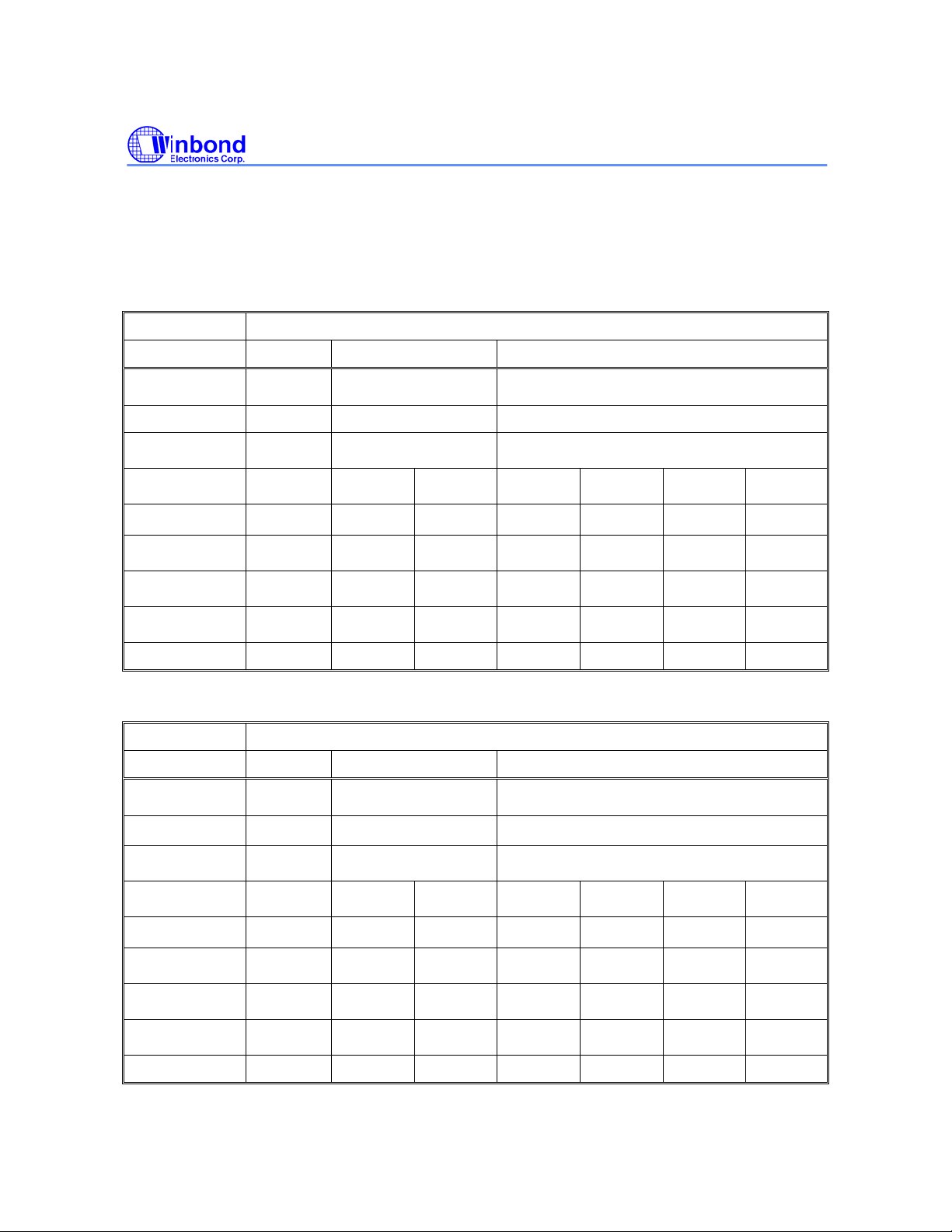
W90P710CD/W90P710CDG
Table 6.2.9 and Table 6.2.10
Using little-endian and word access, Program/Data path between register and external memory
WA = Address whose LSB is 0,4,8,C X = Don’t care
nWBE [3-0] / SDQM [3-0] = A means active and U means inactive
Table6.2.9 Word access write operation with little Endian
Access Operation Write Operation (CPU Register Î External Memory)
XD Width Word Half Word Byte
Bit Number
CPU Reg Data
SA
Bit Number
SD
Bit Number
ED
XA
nWBE [3-0] /
SDQM [3-0]
Bit Number
XD
Bit Number
Ext. Mem Data
Timing Sequence 1st write 2nd write 1st write 2nd write 3rd write 4th write
31 0
ABCD
WA WA WA
31 0
ABCD
31 0
ABCD
WA WA WA+2 WA WA+1 WA+2 WA+3
AAAA XXAA XXAA XXXA XXXA XXXA XXXA
31 0
ABCD
31 0
ABCD
15 0
CD
15 0
CD
15 0
CD
31 0
ABCD
31 0
AB CD
15 0
AB
15 0
AB
15 0
AB
7 0
D
7 0
D
7 0
D
31 0
A B C D
7 0
C
7 0
C
7 0
C
31 0
ABCD
7 0
B
7 0
B
7 0
B
7 0
A
7 0
A
7 0
A
Table6.2.10 Word access read operation with Little Endian
Access Operation Read Operation (CPU Register Í External Memory)
XD Width Word Half Word Byte
Bit Number
CPU Reg Data
SA
Bit Number
SD
Bit Number
ED
XA
31 0
ABCD
WA WA WA
31 0
ABCD
31 0
ABCD
WA WA WA+2 WA WA+1 WA+2 WA+3
31 0
XX CD
31 0
ABCD
31 0
AB CD
31 0
AB CD
31 0
X X X D
31 0
A B C D
31 0
X X C D
31 0
ABCD
31 0
X B C D
31 0
A B C D
SDQM [3-0]
Bit Number
XD
Bit Number
Ext. Mem Data
Timing Sequence 1st read 2nd read 1st read 2nd read 3rd read 4th read
AAAA XXAA XXAA XXXA XXXA XXXA XXXA
31 0
ABCD
31 0
ABCD
15 0
CD
15 0
CD
15 0
AB
15 0
AB
7 0
D
7 0
D
7 0
C
7 0
C
7 0
B
7 0
B
7 0
A
7 0
A
Publication Release Date: September 19, 2006
- 43 - Revision B2
Page 44
W90P710CD/W90P710CDG
Table 6.2.11 and Table 6.2.12
Using little-endian and half-word access, Program/Data path between register and external memory.
HA = Address whose LSB is 0,2,4,6,8,A,C,E HAL = Address whose LSB is 0,4,8,C
HAU = Address whose LSB is 2,6,A,E X = Don’t care
nWBE [3-0] / SDQM [3-0] = A means active and U means inactive
Table6.2.11 Half-word access write operation with little Endian
Access Operation Write Operation (CPU Register Î External Memory)
XD Width Word Half Word Byte
Bit Number
CPU Reg Data
SA
Bit Number
SD
Bit Number
ED
XA
nWBE [3-0] /
SDQM [3-0]
Bit Number
XD
Bit Number
Ext. Mem Data
Timing Sequence 1st write 2nd write
HAL HAU HA HA
31 0
CD CD
31 0
CD CD
HAL HAL HA HA HA+1
UUAA AAUU XXAA XXXA XXXA
31 0
CD CD
15 0
CD
31 0
ABCD
31 0
CD CD
31 0
CD CD
31 0
CD CD
31 16
CD
31 0
ABCD
31 0
CD CD
31 0
CD CD
15 0
CD
15 0
CD
31 0
CD CD
7 0
D
7 0
D
7 0
D
31 0
ABCD
31 0
CD CD
7 0
C
7 0
C
7 0
C
Table6.2.12 Half-word access read operation with Little Endian
Access Operation Read Operation (CPU Register Í External Memory)
XD Width Word Half Word Byte
Bit Number
CPU Reg Data
SA
Bit Number
SD
Bit Number
ED
XA
15 0
CD
HAL HAU HA HA
15 0
CD
15 0
CD
HAL HAL HA HA HA+1
15 0
AB
15 0
AB
15 0
AB
15 0
CD
15 0
CD
15 0
CD
15 0
XD
15 0
CD
15 0
CD
15 0
CD
SDQM [3-0]
Bit Number
XD
Bit Number
Ext. Mem Data
Timing Sequence 1st read 2nd read
UUAA AAUU XXAA XXXA XXXA
31 0
AB CD
31 0
ABCD
31 0
AB CD
15 0
CD
15 0
CD
7 0
D
7 0
D
- 44 -
7 0
C
7 0
C
Page 45
W90P710CD/W90P710CDG
Table 6.2.13 and Table 6.2.14
Using little-endian and byte access, Program/Data path between register and external memory.
BA = Address whose LSB is 0,1,2,3,4,5,6,7,8,9,A,B,C,D,E,F
BAL = Address whose LSB is 0,2,4,6,8,A,C,E BAU = Address whose LSB is 1,3,5,7,9,B,D,F
BA0 = Address whose LSB is 0,4,8,C BA1 = Address whose LSB is 1,5,9,D
BA2 = Address whose LSB is 2,6,A,E BA3 = Address whose LSB is 3,7,B,F
Table6.2.13 Byte access write operation with little Endian
Access Operation Write Operation (CPU Register Î External Memory)
XD Width Word Half Word Byte
Bit Number
CPU Reg Data
SA
Bit Number
SD
Bit Number
ED
XA
nWBE [3-0] /
SDQM [3-0]
Bit Number
XD
Bit Number
Ext. Mem Data
Timing Sequence
BA0 BA1 BA2 BA3 BAL BAU BA
31 0
D D D D
7 0
D
BA0 BA0 BA0 BA0 BAL BAL BA
UUUA UUAU UAUU AUUU XXUA XXAU XXXA
31 0
X X X D
7 0
D
31 0
D D D D
31 0
X X D X
15 8
D
15 8
D
31 0
ABCD
31 0
D D D D
23 16
D
31 0
X D X X
23 16
D
31 0
D D D D
31 24
D
31 0
D X X X
31 24
D
31 0
D D D D
7 0
D
15 0
X D
7 0
D
31 0
ABCD
D D D D
31 0
15 8
D
15 0
D X
15 8
D
31 0
ABCD
31 0
D D D D
7 0
D
7 0
D
7 0
D
Table6.2.14 Byte access read operation with Little Endian
Access Operation Read Operation (CPU Register Í External Memory)
XD Width Word Half Word Byte
Bit Number
CPU Reg Data
SA
Bit Number
SD
Bit Number
ED
XA
SDQM [3-0]
Bit Number
XD
Bit Number
Ext. Mem Data
Timing Sequence
7 0
D
BA0 BA1 BA2 BA3 BAL BAU BA
7 0
D
7 0
D
BA0 BA0 BA0 BA0 BAL BAL BA
UUUA UUAU UAUU AUUU XXUA XXAU XXXA
31 0
ABCD
7 0
C
7 0
C
7 0
C
31 0
ABCD
7 0
B
7 0
B
7 0
B
31 0
ABCD
31 0
ABCD
7 0
A
7 0
A
7 0
A
31 0
ABCD
7 0
D
7 0
D
7 0
D
15 0
CD
7 0
C
7 0
C
7 0
C
15 0
CD
15 0
CD
Publication Release Date: September 19, 2006
- 45 - Revision B2
7 0
D
7 0
D
7 0
D
7 0
D
7 0
D
Page 46

W90P710CD/W90P710CDG
6.2.5 Bus Arbitration
The W90P710’s internal function blocks or external devices can request mastership of the system bus
and then hold the system bus in order to perform data transfers. Because the design of W90P710 bus
allows only one bus master at a time, a bus controller is required to arbitrate when two or more internal
units or external devices simultaneously request bus mastership. When bus mastership is granted to an
internal function block or an external device, other pending requests are not acknowledged until the
previous bus master has released the bus.
W90P710 supports two priority modes, the Fixed Priority Mode and the Rotate Priority Mode, depends
on the ARBCON register PRTMOD bit setting.
6.2.5.1 Fixed Priority Mode
In Fixed Priority Mode (PRTMOD=0, default value), to facilitate bus arbitration, priorities are assigned to
each internal W90P710 function block. The bus controller arbitration requests for the bus mastership
according to these fixed priorities. In the event of contention, mastership is granted to the function block
with the highest assigned priority. These priorities are listed in Table 6.2.15.
W90P710 allows raising ARM Core priority to second if an unmasked interrupt occurred. If IPEN bit, Bit 1
of the Arbitration Control Register (ARBCON), is set to “0”, the priority of ARM Core is fixed to lowest.
If IPEN bit is set to “1” and if no unmasked interrupt request, then the ARM Core’s priority is still lowest
and the IPACT=0, Bit 2 of the Arbitration Control Register (ARBCON) ; If there is an unmasked
interrupt request, then the ARM Core’s priority is raised to first and IPACT=1.
If IPEN is set, an interrupt handler will normally clear IPACT at the end of the interrupt routine to allow an
alternate bus master to regain the bus; however, if IPEN is cleared, no additional action need be taken in
the interrupt handler. The IPACT bit can be read and written. Writing with “0”, the IPACT bit is cleared,
but it will be no effect as writing with “1”.
Table 6.2.15 Bus Priorities for Arbitration in Fixed Priority Mode
BUS FUNCTION BLOCK
PRIORITY IPACT = 0 IPEN = 1 AND IPACT = 1
1 (Highest) Audio Controller (AC97 & I2S) ARM Core
2 LCD Audio Controller (AC97 & I2S)
3 General DMA0 LCD Controller
4 General DMA1 General DMA0
5 EMC DMA General DMA1
6 SD EMC DMA
7 USB Host SD
8 USB Device USB Host
9(Lowest) ARM Core USB Device
- 46 -
Page 47
W90P710CD/W90P710CDG
6.2.5.2 Rotate Priority Mode
In Rotate Priority Mode (PRTMOD=1), the IPEN and IPACT bits have no function (i.e. can be ignored).
W90P710 uses a round robin arbitration scheme ensures that all bus masters have equal chance to gain
the bus and that a retracted master does not lock up the bus.
6.2.6 Power management
W90P710 provide three power management scenarios to reduce power consumption. The
peripherals’ clocks can be enabled / disabled individually by controlling the co-responding bit in
CLKSEL control register. Software can turn-off the unused modules’ clocks to saving the unnecessary
power consumption. It also provides idle and power-down modes to reduce power consumption.
PD
EXTAL
XTAL
Crystal
Oscillator
16-bit
Counter
480MHz
PLL
CLKS
W90P710 Clock Generator
Fig. 6.2.6 W90P710 system clock generation diagram
MIDLE
IDLE
HCLK
EnEMCclk
EnLCDclk
.
.
.
.
.
HCLK_memc
HCLK_cache
HCLK_EMC
.
.
.
.
.
.
.
.
.
.
HCLK_LCD
IDLE MODE
If the IDLE bit in Power Management Control Register (PMCON) is set, the ARM CORE clock source
will be halted, the ARM CORE will not go forward. The AHB or APB clocks still active except the clock
to cache controller and ARM are stopped. W90P710 will exit idle state when nIRQ or nFIQ from any
peripheral is revived; like keypad, timer overflow interrupts and so on. The memory controller can also
be forced to enter idle state if both MIDLE and IDLE bits are set. Software must switch SDRAM into
self-refresh mode before forcing memory to enter idle mode.
Publication Release Date: September 19, 2006
- 47 - Revision B2
Page 48
FOUT
(PLL)
HCLK
idle_state
MCLK
(ARM)
HCLK
(cache)
HCLK
(memc)
W90P710CD/W90P710CDG
IDLE Period
Case1. IDLE=1, PD=0, MIDLE=0
Fig. 6.2.7 Clock management for system idle mode
IDLE Period
FOUT
(PLL)
HCLK
idle_state
MCLK
(ARM)
HCLK
(cache)
HCLK
(memc)
Case2. IDLE=1, PD=0, MIDLE=1
Fig. 6.2.8 Clock management for system and memory idle mode
Power Down Mode
This mode provides the minimum power consumption. When the W90P710 system is not working or
waiting an external event, software can write PD bit “1” to turn off all the clocks includes system crystal
oscillator to let ARM CORE enter sleep mode. In this state, all peripherals are also in sleep mode
since the clock source is stopped. W90P710 will exit power down state when nIRQ/nFIQ is detected.
W90P710 provides external interrupt nIRQ[3:0], keypad, and USB device interfaces to wakeup the
system clock.
- 48 -
Page 49
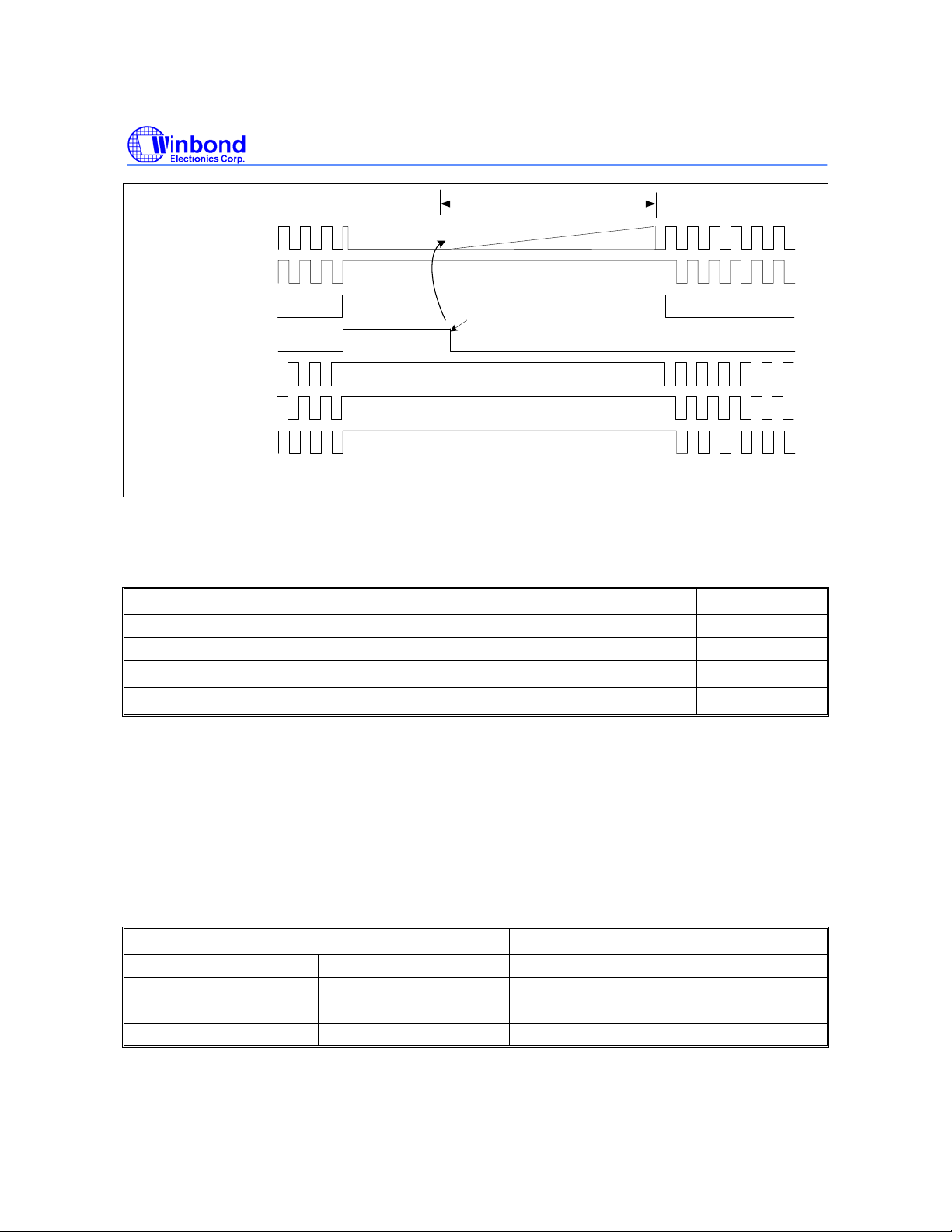
EXTAL
HCLK
W90P710CD/W90P710CDG
65536 clocks
idle _state
pd_state
HCLK
(cache)
Case3. IDLE=0, PD=1, MIDLE=0
Fig 6.2.9 Clock management for system power down mode and wake up
wake up by pheripheral's
interrupts
6.2.7 Power-On Setting
After power on reset, there are eight Power-On setting pins to configure W90P710 system configuration.
POWER-ON SETTING PIN
Internal System Clock Select D15
Little/Big Endian Mode Select D14
Boot ROM/FLASH Data Bus Width
D [13:12]
Default (Always pull-up in normal operation) D [11:8]
D15 pin:Internal System Clock Select
If pin D15 is pull-down, the external clock from EXTAL pin is served as internal system clock.
If pin D15 is pull-up, the PLL output clock is used as internal system clock.
D14 pin:Little/Big Endian Mode Select
If pin D14 is pull-down, the external memory format is Big Endian mode.
If pin D14 is pull-up, the external memory format is Little Endian mode.
D [13:12] : Boot ROM/FLASH Data Bus Width
D [13:12] BUS WIDTH
Pull-down Pull-down 8-bit
Pull-down Pull-up 16-bit
Pull-up Pull-down 32-bit
Pull-up Pull-up RESERVED
Publication Release Date: September 19, 2006
- 49 - Revision B2
Page 50
W90P710CD/W90P710CDG
6.2.8 System Manager Control Registers Map
REGISTER ADDRESS R/W DESCRIPTION RESET VALUE
PDID 0xFFF0_0000 R Product Identifier Register 0xX090_0710
ARBCON 0xFFF0_0004 R/W Arbitration Control Register 0x0000_0000
PLLCON0 0xFFF0_0008 R/W PLL Control Register 0 0x0000_2F01
CLKSEL 0xFFF0_000C R/W Clock Select Register 0x1FFF_3FX8
PLLCON1 0xFFF0_0010 R/W PLL Control Register 1 0x0001_0000
I2SCKCON 0xFFF0_0014 R/W Audio IIS Clock Control Register 0x0000_0000
IRQWAKECON 0xFFF0_0020 R/W IRQ Wakeup Control register 0x0000_0000
IRQWAKEFLAG 0xFFFF_0024 R/W IRQ wakeup Flag Register 0x0000_0000
PMCON 0xFFF0_0028 R/W Power Manager Control Register 0x0000_0000
USBTxrCON 0xFFF0_0030 R/W USB Transceiver Control Register 0x0000_0000
Product Identifier Register (PDID)
This register is read only and lets software use to recognize certain characteristics of the chip ID and the
version number.
REGISTER ADDRESS R/W DESCRIPTION RESET VALUE
PDID 0xFFF0_0000 R Product Identifier Register 0xX090_0710
31 30 29 28 27 26 25 24
PACKAGE VERSION
23 22 21 20 19 18 17 16
CHPID
15 14 13 12 11 10 9 8
CHPID
7 6 5 4 3 2 1 0
CHPID
- 50 -
Page 51
W90P710CD/W90P710CDG
BITS DESCRIPTION
Package Type Select
[31:30] PACKAGE
These two bits are power-on setting latched from pin D[9:8]
Package [31:30] Package Type
1 1 176-pin Package
[29:24] VERSION
[23:0] CHIPID
Version of chip
The chip identifier 0x090.0710
Arbitration Control Register (ARBCON)
REGISTER ADDRESS R/W DESCRIPTION RESET VALUE
ARBCON
31 30 29 28 27 26 25 24
23 22 21 20 19 18 17 16
15 14 13 12 11 10 9 8
7 6 5 4 3 2 1 0
BITS DESCRIPTION
[31:3] RESERVED -
[2] IPACT
[1] IPEN
[0] PRTMOD
0xFFF0_0004 R/W
RESERVED IPACT IPEN PRTMOD
Interrupt priority active.
When IPEN=”1”, this bit will be set when the ARM core has an
unmasked interrupt request. This bit is available only when the
PRTMOD=0.
Interrupt priority enable bit
0 = the ARM core has the lowest priority.
1 = enable to raise the ARM core priority to second
This bit is available only when the PRTMOD=0.
Priority mode select
0 = Fixed Priority Mode (default)
1 = Rotate Priority Mode
Arbitration Control Register
RESERVED
RESERVED
RESERVED
0x0000_0000
Publication Release Date: September 19, 2006
- 51 - Revision B2
Page 52
W90P710CD/W90P710CDG
PLL Control Register0 (PLLCON0)
W90P710 provides two clock generation options – crystal and oscillator. The external clock via
EXTAL(15M) Minput pin as the reference clock input of PLL module. The external clock can bypass the
PLL and be used to the internal system clock by pull-down the data D15 pin. Using PLL’s output clock
for the internal system clock, D15 pin must be pull-up.
REGISTER ADDRESS R/W DESCRIPTION RESET VALUE
PLLCON
31 30 29 28 27 26 25 24
23 22 21 20 19 18 17 16
0xFFF0_0008 R/W
RESERVED
RESERVED PWDEN
PLL Control Register
0x0000_2F01
15 14 13 12 11 10 9 8
FBDV
7 6 5 4 3 2 1 0
FBDV OTDV INDV
BITS DESCRIPTION
[31:17] RESERVED -
Power down mode enable
[16] PWDEN
[15:7] FBDV
[6:5] OTDV
[4:0] INDV
0 = PLL is in normal mode (default)
1 = PLL is in power down mode
PLL VCO output clock feedback divider
Feedback Divider divides the output clock from VCO of PLL.
PLL output clock divider
OTDV [6:5] DIVIDED BY
0 0 1
0 1 2
1 0 2
PLL input clock divider
Input divider divides the input reference clock into the PLL.
1 1 4
- 52 -
Page 53
W90P710CD/W90P710CDG
O
EXTAL
FIN
INDV[4:0]
FBDV[8:0]
Input Divider
(NR)
PFD
Feedback
Divider
(NF)
Charge
Pump
Fig 6.2.8.1 System PLL block diagram
The formula of output clock of PLL is:
NF 1
FOUT = FIN
NR
∗∗
N
FOUT:Output clock of Output Divider
FIN:External clock into the Input Divider
NR:Input divider value (NR = INDV + 2)
NF:Feedback divider value (NF = FBDV + 2)
NO:Output divider value (NO = OTDV)
PLL
VCO
Output
Divider
(NO)
OTDV[1:0]
480MHz
FOUT
GP0
48MHz
Gen
Clock
Divider
&
Selector
CLKS[2:0]
USBCKS
1
0
0
1
ECLKS
USB
Module
Internal
System
Clock
Clock Select Register (CLKSEL)
REGISTER ADDRESS R/W DESCRIPTION RESET VALUE
CLKSEL
0xFFF0_000C R/W
31 30 29 28 27 26 25 24
RESERVED PS2 KPI SCH1 SCH0 SSP
23 22 21 20 19 18 17 16
UART3 UART2 UART1 I2C1 I2C0 RTC PWM AC97
15 14 13 12 11 10 9 8
USBCKS USBD GDMA SD LCD EMC RESERVED WDT
7 6 5 4 3 2 1 0
USBH TIMER UART ECLKS CLKS RESET
Clock Select Register
0x1FFF_7FX8
Publication Release Date: September 19, 2006
- 53 - Revision B2
Page 54

W90P710CD/W90P710CDG
BITS DESCRIPTION
[31:29] RESERVED -
PS2 controller clock enable bit
[28] PS2
[27] KPI
[26] SCH1
[25] SCH0
[24] USI
[23] UART3
[22] UART2
[21] UART1
[20] I2C1
[19] I2C0
[18] RTC
0 = Disable PS2 controller clock
1 = Enable PS2 controller clock
Keypad controller clock enable bit
0 = Disable keypad controller clock
1 = Enable keypad controller clock
Smart Card Host controller 1 clock enable bit
0 = Disable smart card host controller 1 clock
1 = Enable smart card host controller 1 clock
Smart Card Host controller 0 clock enable bit
0 = Disable smart card host controller 0 clock
1 = Enable smart card host controller 0 clock
USI controller clock enable bit
0 = Disable USI controller clock
1 = Enable USI controller clock
UART3 controller clock enable bit
0 = Disable UART3 controller clock
1 = Enable UART3 controller clock
UART2 controller clock enable bit
0 = Disable UART2 controller clock
1 = Enable UART2 controller clock
UART1 controller clock enable bit
0 = Disable UART1 controller clock
1 = Enable UART1 controller clock
I2C1 controller clock enable bit
0 = Disable I2C1 controller clock
1 = Enable I2C1 controller clock
I2C0 controller clock enable bit
0 = Disable I2C0 controller clock
1 = Enable I2C0 controller clock
RTC unit clock enable bit
0 = Disable RTC controller clock
1 = Enable RTC controller clock
- 54 -
Page 55

W90P710CD/W90P710CDG
Continued.
BITS DESCRIPTION
PWM controller clock enable bit
[17] PWM
[16] AC97
[15] USBCKS
[14] USBD
[13] GDMA
[12] SD
[11] LCD
[10] EMC
[9] RESERVED
[8] WDT
[7] USBH
[6] TIMER
0 = Disable PWM controller clock
1 = Enable PWM controller clock
Audio Controller clock enable bit
0 = Disable AC97 controller clock
1 = Enable AC97 controller clock
USB host/device 48MHz clock source Select bit
0 = USB clock 48MHz input from internal PLL (480MHz/10)
1 = USB clock 48MHz input from external GPIO0 pin, this pin direction
must set to input.
USB device clock enable bit
0 = Disable USB device controller clock
1 = Enable USB device controller clock
GDMA controller clock enable bit
0 = Disable GDMA clock
1 = Enable GDMA clock
SD host controller clock enable bit
0 = Disable SD controller clock
1 = Enable SD controller clock
LCD controller clock enable bit
0 = Disable LCD controller clock
1 = Enable LCD controller clock
EMC controller clock enable bit
0 = Disable EMC controller clock
1 = Enable EMC controller clock
-
WDT clock enable bit
0 = Disable WDT counting clock
1 = Enable WDT counting clock
USB host clock enable bit
0 = Disable USB host controller clock
1 = Enable USB host controller clock
Timer clock enable bit
0 = Disable timer clock
1 = Enable timer clock
Publication Release Date: September 19, 2006
- 55 - Revision B2
Page 56
W90P710CD/W90P710CDG
Continued.
BITS DESCRIPTION
UART0 controller clock enable bit
[5] UART0
[4] ECLKS
[3:1] CLKS
0 = Disable UART0 controller clock
1 = Enable UART0 controller clock
External clock select
0 = External clock from EXTAL pin is used as system clock
1 = PLL output clock is used as system clock
After power on reset, the content of ECLKS is the Power-On Setting
value. You can program this bit to change the system clock source.
PLL output clock select
CLKS [3:1] System clock
0 0 0 58.594 KHz*
0 0 1 24 MHz
0 1 0 48 MHz
0 1 1 60 MHz
1 0 0 80 MHz
1 0 1 RESERVED
1 1 0 RESERVED
1 1 1 RESERVED
[0] RESET
Note:
1. This values are based on PLL output(FOUT) is 480MHz.
2. When 24Mhz ~ 80MHz is selected, the ECLKS bit must be set to 1.
3. About 58.594KHz setting, two steps are needed. First, clear ECLKS
bit, and then clear CLKS.
Software Reset bit
This is a software reset control bit. Set logic 1 to generate an internal
reset pulse. This bit is auto-clear to logic 0 at the end of the reset pulse.
- 56 -
Page 57
W90P710CD/W90P710CDG
PLL Control Register 1(PLLCON1)
W90P710 provides extra PLL for LCD controller programmable pixel clock and provide 12.288/16.934
MHz clock source to Audio Controller. It uses the same 15MHz crystal clock input source with system
PLL mentioned above.
REGISTER ADDRESS R/W DESCRIPTION RESET VALUE
PLLCON1
31 30 29 28 27 26 25 24
23 22 21 20 19 18 17 16
15 14 13 12 11 10 9 8
0xFFF0_0010 R/W
RESERVED PWDEN1
PLL Control Register 1
RESERVED
FBDV1
0x0001_0000
7 6 5 4 3 2 1 0
FBDV1 OTDV1 INDV1
BITS DESCRIPTION
[31:17] RESERVED -
PLL1 power down enable
[16] PWDEN1
[15:7] FBDV1
[6:5] OTDV1
[4:0] INDV1
0 = PLL1 is in normal mode
1 = PLL1 is in power down mode (default)
PLL1 VCO output clock feedback divider
Feedback Divider divides the output clock from VCO of PLL1.
PLL1 output clock divider
OTDV1 [6:5] Divided by
0 0 1
0 1 2
1 0 2
1 1 4
PLL1 input clock divider
Input divider divides the input reference clock into the PLL1.
Publication Release Date: September 19, 2006
- 57 - Revision B2
Page 58
INDV1[4:0]
EXTAL
FIN
Input Divider
(NR)
PLL1
W90P710CD/W90P710CDG
to LCD controller
Charge
Pump
Fig 6.2.8.2 LCD PLL block diagram
FBDV1[8:0]
PFD
Feedback
Divider
(NF)
The formula of output clock of PLL is:
FOUT = FIN
NF 1
∗∗
NONR
FOUT:Output clock of Output Divider
FIN:External clock into the Input Divider
NR:Input divider value (NR = INDV1 + 2)
NF:Feedback divider value (NF = FBDV1 + 2)
NO:Output divider value (NO = OTDV1)
VCO
Output
Divider
OTDV1[1:0]
480MHz
(NO)
FOUT
to Audio Controller
- 58 -
Page 59
W90P710CD/W90P710CDG
IIS Clock Control Register (I2SCKCON)
REGISTER ADDRESS R/W DESCRIPTION RESET VALUE
I2SCKCON
31 30 29 28 27 26 25 24
23 22 21 20 19 18 17 16
15 14 13 12 11 10 9 8
7 6 5 4 3 2 1 0
BITS DESCRIPTION
[31:9] RESERVED -
[8] I2SPLLEN
0xFFF0_0014 R/W
RESERVED IISPLLEN
IIS PLL clock source enable
Set this bit will enable PLL1 clock output to audio I2S clock input.
1 = Enable PLL1 clock source for audio I2S
0 = Disable PLL1 clock source for audio I2S
I2S PLL clock Control Register
RESERVED
RESERVED
PRESCALE
0x0000_0000
The PLL1 is shared with LCD controller, if both the LCD and I2S are
using the PLL at the same time, software can using this prescaler
[7:0] PRESCALE
to generate an appropriate clock nearly 12.288M or 16.934M. The
clock is generated as below, and if PRESCALE =0, the
PLL_AUDIO is the same frequency as FOUT “PLL_AUDIO =
PLL_FOUT/(PRESCALE +1)”
IRQ Wakeup Control Register (IRQWAKECON)
REGISTER ADDRESS R/W DESCRIPTION RESET VALUE
IRQWAKECON
31 30 29 28 27 26 25 24
23 22 21 20 19 18 17 16
15 14 13 12 11 10 9 8
7 6 5 4 3 2 1 0
0xFFF0_0020 R/W
RESERVED
IRQWAKEUPPOL IRQWAKEUPEN
IRQ Wakeup Control Register
RESERVED
RESERVED
0x0000_0000
Publication Release Date: September 19, 2006
- 59 - Revision B2
Page 60
W90P710CD/W90P710CDG
BITS DESCRIPTION
[31:8] RESERVED
nIRQ3 wake up polarity
[7] IRQWAKEUPPOL[3]
[6] IRQWAKEUPPOL[2]
[5] IRQWAKEUPPOL[1]
[4] IRQWAKEUPPOL[0]
1 = nIRQ3 is high level wake up
0 = nIRQ3 is low level wake up
nIRQ2 wake up polarity
1 = nIRQ2 is high level wake up
0 = nIRQ2 is low level wake up
nIRQ1 wake up polarity
1 = nIRQ1 is high level wake up
0 = nIRQ1 is low level wake up
nIRQ0 wake up polarity
1 = nIRQ0 is high level wake up
0 = nIRQ0 is low level wake up
nIRQ3 wake up enable bit
[3] IRQWAKEUPEN[3]
[2] IRQWAKEUPEN[2]
[1] IRQWAKEUPEN[1]
[0] IRQWAKEUPEN[0]
1 = nIRQ3 wake up enable
0 = nIRQ3 wake up disable
nIRQ2 wake up enable bit
1 = nIRQ2 wake up enable
0 = nIRQ2 wake up disable
nIRQ1 wake up enable bit
1 = nIRQ1 wake up enable
0 = nIRQ1 wake up disable
nIRQ0 wake up enable bit
1 = nIRQ0 wake up enable
0 = nIRQ0 wake up disable
IRQ Wakeup Flag Register (IRQWAKEFLAG)
REGISTER ADDRESS R/W DESCRIPTION RESET VALUE
IRQWAKEFLAG
0xFFF0_0024 R/W
IRQ Wakeup Flag Register
0x0000_0000
- 60 -
Page 61
W90P710CD/W90P710CDG
31 30 29 28 27 26 25 24
RESERVED
23 22 21 20 19 18 17 16
RESERVED
15 14 13 12 11 10 9 8
RESERVED
7 6 5 4 3 2 1 0
RESERVED
This register is used to record the wakeup events, after clock recovery, software should check these
flags to identify which nIRQ is used to wakeup the system. And clear the flags in IRQ interrupt sevice
routine.
BITS DESCRIPTION
[31:4] RESERVED -
nIRQ3 wake up flag
[3] IRQWAKEFLAG[3]
[2] IRQWAKEFLAG[2]
[1] IRQWAKEFLAG[1]
[0] IRQWAKEFLAG[0]
1 = Chip is waked up by nIRQ3
0 = No active
nIRQ2 wake up flag
1 = Chip is waked up by nIRQ2
0 = No active
nIRQ1 wake up flag
1 = Chip is waked up by nIRQ1
0 = No active
nIRQ0 wake up flag
1 = Chip is waked up by nIRQ0
0 = No active
IRQWAKEFLAG
Power Management Control Register (PMCON)
REGISTER ADDRESS R/W DESCRIPTION RESET VALUE
PMCON
31 30 29 28 27 26 25 24
23 22 21 20 19 18 17 16
15 14 13 12 11 10 9 8
7 6 5 4 3 2 1 0
0xFFF0_0028 R/W
RESERVED
Power Management Control Register
RESERVED
RESERVED
RESERVED
MIDLE PD IDLE
Publication Release Date: September 19, 2006
- 61 - Revision B2
0x0000_0000
Page 62
W90P710CD/W90P710CDG
e
e
p
e
s
E
BITS DESCRIPTION
[31:3] RESERVED
Memory controller IDLE enable
Setting both MIDLE and IDLE bits HIGH will let memory controller
enter IDLE mode, the clock source of memory controller will be halted
while ARM CORE enter IDLE mode.
[2] MIDLE
[1] PD
1=memory controller will be forced into IDLE mode, (clock of memory
controller will be halted), when IDLE bit is set.
0 = memory controller still active when IDLE bit is set.
NOTE: Software must let SDRAM enter self-refresh mode before
enable this function because SDRAM MCLK will be stopped.
Power down enable
Setting this bit HIGH will let W90P710 enter power saving mode. Th
clock source 15M crystal oscillator and PLLs are stopped to generat
clock. User can use nIRQ[3:0], keypad and external RESET to wakeu
W90P710.
1 = Enable power down
0 = Disable
IDLE mode enable
Setting this bit HIGH will let ARM Core enter power saving mode. Th
peripherals can still keep working if the clock enable bit in CLKSEL i
[0] IDLE
set. Any nIRQ or nFIQ to ARM Core will let ARM CORE to exit IDL
state.
1 = IDLE mode
0 = Disable
USB Transceiver Control Register (USBTXRCON)
REGISTER ADDRESS R/W DESCRIPTION RESET VALUE
USBTXRCO
N
31 30 29 28 27 26 25 24
23 22 21 20 19 18 17 16
15 14 13 12 11 10 9 8
7 6 5 4 3 2 1 0
0xFFF0_0030 R/W
RESERVED
USB Transceiver Control Register
RESERVED
RESERVED
RESERVED
0x0000_0000
USBHnD
- 62 -
Page 63

W90P710CD/W90P710CDG
BITS DESCRIPTION
[31:1] RESERVED -
USBHnD[0]: USB transceiver control
There are two USB1.1 built-in transceivers for data transmission. One
[0]
USBHnD
is dedicated for USB host and the other is shared with USB device.
Software can program this bit to switch the transceiver path.
1 = HOST
0 = Device
Publication Release Date: September 19, 2006
- 63 - Revision B2
Page 64

W90P710CD/W90P710CDG
6.3 External Bus Interface
6.3.1 EBI Overview
W90P710 supports External Bus Interface (EBI), which controls the access to the external memory
(ROM/FLASH, SDRAM) and External I/O devices. The EBI has seven chip selects to select one
ROM/FLASH bank, two SDRAM banks, and four External I/O banks.The address bus is 22 bits. It
supports 8-bit, 16-bit, and 32-bit external data bus width for each bank.
The EBI has the following functions:
y SDRAM controller
y EBI control register
y ROM/FLASH interface
y External I/O interface
y External bus mastership
6.3.2 SDRAM Controller
The SDRAM controller module within W90P710 contains configuration registers 、 timing control
registers、common control register and other logic to provide 8、16、32 bits SDRAM interface with a
single 8、16、32 bits SDRAM device or two 8-bit devices wired to give a 16-bit data path or two 16-bit
devices wired to give a 32-bit data path. The maximum size of each bank is 64M bytes, and maximum
memory size can span up to 128MB.
The SDRAM controller has the following features:
y Supports up to 2 external SDRAM banks
y Maximum size of each bank is 64M bytes
y 8、16、32-bit data interface
y Programmable CAS Latency: 1、2 and 3
y Fixed Burst Length: 1
y Sequential burst type
y Auto Refresh Mode and Self Refresh Mode
y Adjustable Refresh Rate
y Power up sequence
- 64 -
Page 65
W90P710CD/W90P710CDG
6.3.2.1 SDRAM Components Supported
Table 6.3.2.1 SDRAM supported by W90P710
SIZE TYPE BANKS ROW ADDRESSING COLUMN ADDRESSING
16M bits 2Mx8 2 RA0~RA10 CA0~CA8
1Mx16 2 RA0~RA10 CA0~CA7
64M bits 8Mx8 4 RA0~RA11 CA0~CA8
4Mx16 4 RA0~RA11 CA0~CA7
2Mx32 4 RA0~RA10 CA0~CA7
128M bits 16Mx8 4 RA0~RA11 CA0~CA9
256M bits 32Mx8 4 RA0~RA12 CA0~CA9
16Mx16 4 RA0~RA12 CA0~CA8
AHB Bus Address Mapping to SDRAM Bus
Note: * indicates the signal is not used; ** indicates the signal is fixed at logic 0 and is not used;
The HADDR prefixes have been omitted on the following tables.
A14 ~ A0 are the Address pins of the W90P710 EBI interface;
A14 and A13 are the Bank Select Signals of SDRAM.
SDRAM Data Bus Width: 32-bit
Total Type R x C R/C
16M 2Mx8 11x9 R ** 11 ** 11* 22 21 20 19 18 17 16 15 14 13 12
C ** 11 ** 11* AP 25* 10 9 8 7 6 5 4 3 2
16M 1Mx16 11x8 R ** 10 ** 10* 11 21 20 19 18 17 16 15 14 13 12
C ** 10 ** 10* AP 25* 10* 9 8 7 6 5 4 3 2
64M 8Mx8 12x9 R 11 12 11* 23 22 21 20 19 18 17 16 15 14 13 24
C 11 12 11* 23* AP 25* 10 9 8 7 6 5 4 3 2
64M 4Mx16 12x8 R 11 10 11* 23 22 21 20 19 18 17 16 15 14 13 12
C 11 10 11* 23* AP 25* 24* 9 8 7 6 5 4 3 2
64M 2Mx32 11x8 R 11 10 11* 23* 22 21 20 19 18 17 16 15 14 13 12
C 11 10 11* 23* AP 25* 24* 9 8 7 6 5 4 3 2
128M* 16Mx8 12x10 R 11 12 11* 23 22 21 20 19 18 17 16 15 14 13 24
C 11 12 11* 23* AP 25 10 9 8 7 6 5 4 3 2
128M 8Mx16 12x9 R 11 12 11* 23 22 21 20 19 18 17 16 15 14 13 24
C 11 12 11* 23* AP 25* 10 9 8 7 6 5 4 3 2
128M 4Mx32 12x8 R 11 10 11* 23 22 21 20 19 18 17 16 15 14 13 12
C 11 10 11* 23* AP 25* 10* 9 8 7 6 5 4 3 2
256M* 32Mx8 13x10 R 11 12 24 23 22 21 20 19 18 17 16 15 14 13 25
C 11 12 24* 23* AP 26* 10 9 8 7 6 5 4 3 2
256M* 16Mx16 13x9 R 11 12 24 23 22 21 20 19 18 17 16 15 14 13 25
C 11 12 24* 23* AP 26* 10* 9 8 7 6 5 4 3 2
8Mx16 4 RA0~RA11 CA0~CA8
4Mx32 4 RA0~RA11 CA0~CA7
A14
A13
(BS1)
(BS0)
A12 A11 A10 A9 A8 A7 A6 A5 A4 A3 A2 A1 A0
Publication Release Date: September 19, 2006
- 65 - Revision B2
Page 66

W90P710CD/W90P710CDG
SDRAM Data Bus Width: 16-bit
A14
Total Type R x C R/C
16M 2Mx8 11x9 R
C
16M 1Mx16 11x8 R
C
64M 8Mx8 12x9 R 10 11
C 10 11
64M 4Mx16 12x8 R 10 9
C 10 9
64M 2Mx32 11x8 R 10 9
C 10 9
128M 16Mx8 12x10 R 10 11
C 10 11
128M 8Mx16 12x9 R 10 11
C 10 11
128M 4Mx32 12x8 R 10 9
C 10 9
256M* 32Mx8 13x10 R 10 11 23 22 21 20 19 18 17 16 15 14 13 12
C 10 11
256M 16Mx16 13x9 R 10 11 23 22 21 20 19 18 17 16 15 14 13 12
C 10 11
(BS1)
A13
(BS0)
**
** 10 ** 10*
**
**
A12 A11 A10 A9 A8 A7 A6 A5 A4 A3 A2 A1 A0
10
** 10*
9
** 9* 10
9
** 9*
22 21 20 19 18 17 16 15 14 13 12
10*
10* 22*
22 21 20 19 18 17 16 15 14 13 12 11
10*
10* 22*
10* 22*
10* 22*
22 21 20 19 18 17 16 15 14 13 12
10*
10* 22*
22 21 20 19 18 17 16 15 14 13 12
10*
10* 22*
22 21 20 19 18 17 16 15 14 13 12 11
10*
10* 22*
23* 22*
23* 22*
21 20 19 18 17 16 15 14 13 12 11
AP
24* 9 8 7 6 5 4 3
20 19 18 17 16 15 14 13 12 11
AP
24* 9* 8765 4 3
AP
24* 9 8 7 6 5 4 3
AP
24* 23* 8765 4 3
21 20 19 18 17 16 15 14 13 12 11
AP
24* 23* 8765 4 3
AP
24 9 8 7 6 5 4 3
AP
24* 9 8 7 6 5 4 3
AP
24* 9* 8765 4 3
AP
25* 9 8 7 6 5 4 3
AP
25*
9
8765 4 3
21
21
23
21
21
21
23
21
23
21
21
24
21
24
21
- 66 -
Page 67

W90P710CD/W90P710CDG
SDRAM Data Bus Width: 8-bit
A14
Total Type R x C R/C
16M 2Mx8 11x9 R
C
16M 1Mx16 11x8 R
C
64M 8Mx8 12x9 R 9 10
C 9 10
64M 4Mx16 12x8 R 9 8
C 9 8
64M 2Mx32 11x8 R 9 8
C 9 8
128M 16Mx8 12x10 R 9 10
C 9 10
128M 8Mx16 12x9 R 9 10
C 9 10
128M 4Mx32 12x8 R 9 8
C 9 8
256M 32Mx8 13x10 R 9 10 22 21 20 19 18 17 16 15 14 13 12 11
C 9 10
256M 16Mx16 13x9 R 9 10 22 21 20 19 18 17 16 15 14 13 12 11
C 9 10
A13
(BS1)
(BS0)
**
** 9 ** 9*
**
**
A12 A11 A10 A9 A8 A7 A6 A5 A4 A3 A2 A1 A0
9
** 9*
8
** 8* 9
8
** 8*
9*
9* 21*
9*
9* 21*
9* 21*
9* 21*
9*
9* 21*
9*
9* 21*
9*
9* 21*
22* 21*
22* 21*
20 19 18 17 16 15 14 13 12 11 10
AP
23* 87654 3
19 18 17 16 15 14 13 12 11 10
AP
23* 8* 7654 3
21 20 19 18 17 16 15 14 13 12 11
AP
23* 87654 3
21 20 19 18 17 16 15 14 13 12 11 10
AP
23* 22* 7654 3
20 19 18 17 16 15 14 13 12 11 10
AP
23* 22* 7654 3
21 20 19 18 17 16 15 14 13 12 11
AP
23 8 7 6 5 4 3
21 20 19 18 17 16 15 14 13 12 11
AP
23* 87654 3
21 20 19 18 17 16 15 14 13 12 11 10
AP
23* 8* 7654 3
AP 24
AP
87654 3
8
24*
7654 3
2 1 0
2 1 0
2 1 1
2 1 0
2 1 0
2 1 0
2 1 0
2 1 0
2 1 0
2 1 0
22
22
22
23
23
6.3.2.2 SDRAM Power Up Sequence
The SDRAM must be initialized predefined manner after power on.W90P710 SDRAM Controller
automatically executes the commands needed for initialion and set the mode register of each bank to
default value. The default value is:
— Burst Length = 1
— Burst Type = Sequential (fixed)
— CAS Latency = 2
— Write Burst Length = Burst (fixed)
The value of mode register can be changed after power up sequence by setting the value of
corresponding bank’s configuration register “LENGTH” and “LATENCY” bits and set the MRSET bit
enable to execute the Mode Register Set command.
Publication Release Date: September 19, 2006
- 67 - Revision B2
Page 68
6.3.2.3 SDRAM Interface
W90P710CD/W90P710CDG
A[21:0]
D[31:0]
MCLK
MCKE
nSCS[1:0]
nSRAS
nSCAS
nSWE
nSDQM[3:0]
W90P710
A[10:0]
nSCS0
nSDQM[3:0]
Fig 6.3.1 SDRAM Interface
A13
A14
A[10:0]
BS0
BS1
DQ[[31:0]
CLK
CKE
nCS
nRAS
nCAS
nWE
DQM[3:0]
SDRAM
64Mb 512Kx4x32
6.3.3 EBI Control Registers Map
REGISTER ADDRESS R/W DESCRIPTION RESET VALUE
EBICON
ROMCON
0xFFF0_1000
0xFFF0_1004
SDCONF0 0xFFF0_1008 R/W SDRAM bank 0 configuration register
SDCONF1 0xFFF0_100C R/W SDRAM bank 1 configuration register
SDTIME0 0xFFF0_1010 R/W SDRAM bank 0 timing control register
SDTIME1
EXT0CON
EXT1CON
EXT2CON
EXT3CON
CKSKEW
0xFFF0_1014
0xFFF0_1018
0xFFF0_101C
0xFFF0_1020
0xFFF0_1024
0xFFF0_1F00
R/W EBI control register
R/W ROM/FLASH control register
R/W SDRAM bank 1 timing control register
R/W External I/O 0 control register
R/W External I/O 1 control register
R/W External I/O 2 control register
R/W External I/O 3 control register
R/W Clock skew control register (for testing)
0x0001_0000
0x0000_0XFC
0x0000_0800
0x0000_0800
0x0000_0000
0x0000_0000
0x0000_0000
0x0000_0000
0x0000_0000
0x0000_0000
0xXXXX_0038
- 68 -
Page 69
W90P710CD/W90P710CDG
EBI Control Register (EBICON)
REGISTER ADDRESS R/W DESCRIPTION RESET VALUE
EBICON
31 30 29 28 27 26 25 24
23 22 21 20 19 18 17 16
15 14 13 12 11 10 9 8
7 6 5 4 3 2 1 0
0xFFF0_1000
RESERVED EXBE3 EXBE2 EXBE1 EXBE0
RESERVED REFEN REFMOD CLKEN
REFRAT WAITVT LITTLE
R/W EBI control register
REFRAT
0x0001_0000
BITS DESCRIPTION
[31:28] RESERVED
External IO bank 3 byte enable
This function is used for some devices that with high and low bytes
enable signals to control which byte will be write or mask data output
[27] EXBE3
[26] EXBE2
[25] EXBE1
when read. For this kind device, software can set this bit HIGH to
implement this function. Detail pin interconnection is showed as Fig6.3.8.
1 = nWBE[3:0] pin is byte enable signals, nWE will be used as write
strobe signal to SRAM.
0 = nWBE[3:0] pin is byte write strobe signal.
External IO bank 2 byte enable
The bit function description is the same as EXBE3 above.
1 = nWBE[3:0] pin is byte enable signals, nWE will be used as write
strobe signal to SRAM.
0 = nWBE[3:0] pin is byte write strobe signal.
External IO bank 1 byte enable
The bit function description is the same as EXBE3 above.
1 = nWBE[3:0] pin is byte enable signals, nWE will be used as write
strobe signal to SRAM
0 = nWBE[3:0] pin is byte write strobe signal
Publication Release Date: September 19, 2006
- 69 - Revision B2
Page 70

W90P710CD/W90P710CDG
Continued.
BITS DESCRIPTION
External IO bank 0 byte enable
This bit function description is the same as EXBE3 above.
[24] EXBE0
[23:19] RESERVED
[18] REFEN
[17] REFMOD
[16] CLKEN
1 = nWBE[3:0] pin is byte enable signals, nWE will be used as write
strobe signal to SRAM
0 = nWBE[3:0] pin is byte write strobe signal
Enable SDRAM refresh cycle for SDRAM bank0 & bank1
This bit set will start the auto-refresh cycle to SDRAM. The refresh rate is
according to REFRAT bits.
1 = Enable refresh function
0 = Disable refresh function
Refresh mode of SDRAM for SDRAM bank
Defines the refresh mode type of external SDRAM bank
Software can write this bit “1” to force SDRAM enter self-refresh mode.
0 = Auto refresh mode
1 = Self refresh mode
NOTE: If any read/write to SDRAM occurs then this bit will be cleared to
“0” by hardware automatically and SDRAM will enter auto-refresh mode.
Clock enable for SDRAM
Enables the SDRAM clock enable (CKE) control signal
0 = Disable (power down mode)
1 = Enable (Default)
Refresh count value for SDRAM
The SDRAM Controller automatically provides an auto refresh cycle for
every refresh period programmed into the REFRAT bits when the
[15:3] REFRAT
REFEN bit of each bank is set
The refresh period is calculated as
- 70 -
period =
value
fMCLK
Page 71
W90P710CD/W90P710CDG
Continued.
BITS DESCRIPTION
Valid time of nWAIT signal
W90P710 recognizes the nWAIT signal at the next “nth” MCLK rising
edge after the nOE or nWBE active cycle. WAITVT bits determine the n.
[2:1] WAITVT
Little Endian mode
After power on reset, the content of LITTLE is the Power-On Setting
value from D14 pin. If pin D14 is pull-down, the external memory format
[0] LITTLE
is Big Endian mode. If pin D14 is pull-up, the external memory format is
Little Endian mode. For more detail, refer to Power-On Setting of System
Manager.
NOTE: This bit is read only.
WAITVT [2:1] nth MCLK
0 0 1
0 1 2
1 0 3
1 1 4
ROM/Flash Control Register (ROMCON)
REGISTER ADDRESS R/W DESCRIPTION RESET VALUE
ROMCON
31 30 29 28 27 26 25 24
23 22 21 20 19 18 17 16
15 14 13 12 11 10 9 8
7 6 5 4 3 2 1 0
0xFFF0_1004
BASADDR SIZE
RESERVED tPA
tACC BTSIZE PGMODE
R/W ROM/FLASH control register
BASADDR
0x0000_0XFC
Publication Release Date: September 19, 2006
- 71 - Revision B2
Page 72
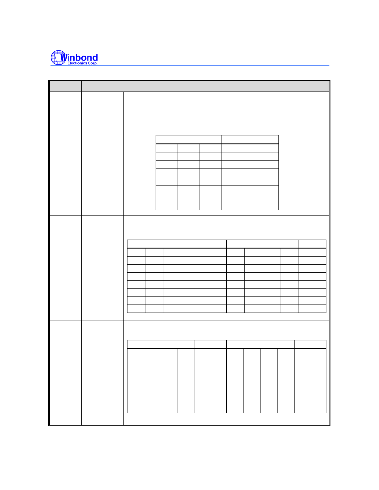
W90P710CD/W90P710CDG
BITS DESCRIPTION
Base address pointer of ROM/Flash bank
[31:19] BASADDR
[18:16] SIZE
The start address is calculated as ROM/Flash bank base pointer << 18.
The base address pointer together with the “SIZE” bits constitutes the
whole address range of each bank.
The size of ROM/FLASH memory
SIZE [10:8] Byte
0 0 0 256K
0 0 1 512K
0 1 0 1M
0 1 1 2M
1 0 0 4M
1 0 1 8M
1 1 0 16M
1 1 1 RESERVED
[15:12] RESERVED
[11:8] tPA
[7:4] tACC
-
Page mode access cycle time
tPA[11:8] MCLK tPA[11:8] MCLK
0 0 0 0 1 1 0 0 0 10
0 0 0 1 2 1 0 0 1 12
0 0 1 0 3 1 0 1 0 14
0 0 1 1 4 1 0 1 1 16
0 1 0 0 5 1 1 0 0 18
0 1 0 1 6 1 1 0 1 20
0 1 1 0 7 1 1 1 0 22
0 1 1 1 8 1 1 1 1 24
Access cycle time
tACC[11:8] MCLK tACC[11:8] MCLK
0 0 0 0 1 1 0 0 0 10
0 0 0 1 2 1 0 0 1 12
0 0 1 0 3 1 0 1 0 14
0 0 1 1 4 1 0 1 1 16
0 1 0 0 5 1 1 0 0 18
0 1 0 1 6 1 1 0 1 20
0 1 1 0 7 1 1 1 0 22
0 1 1 1 8 1 1 1 1 24
- 72 -
Page 73
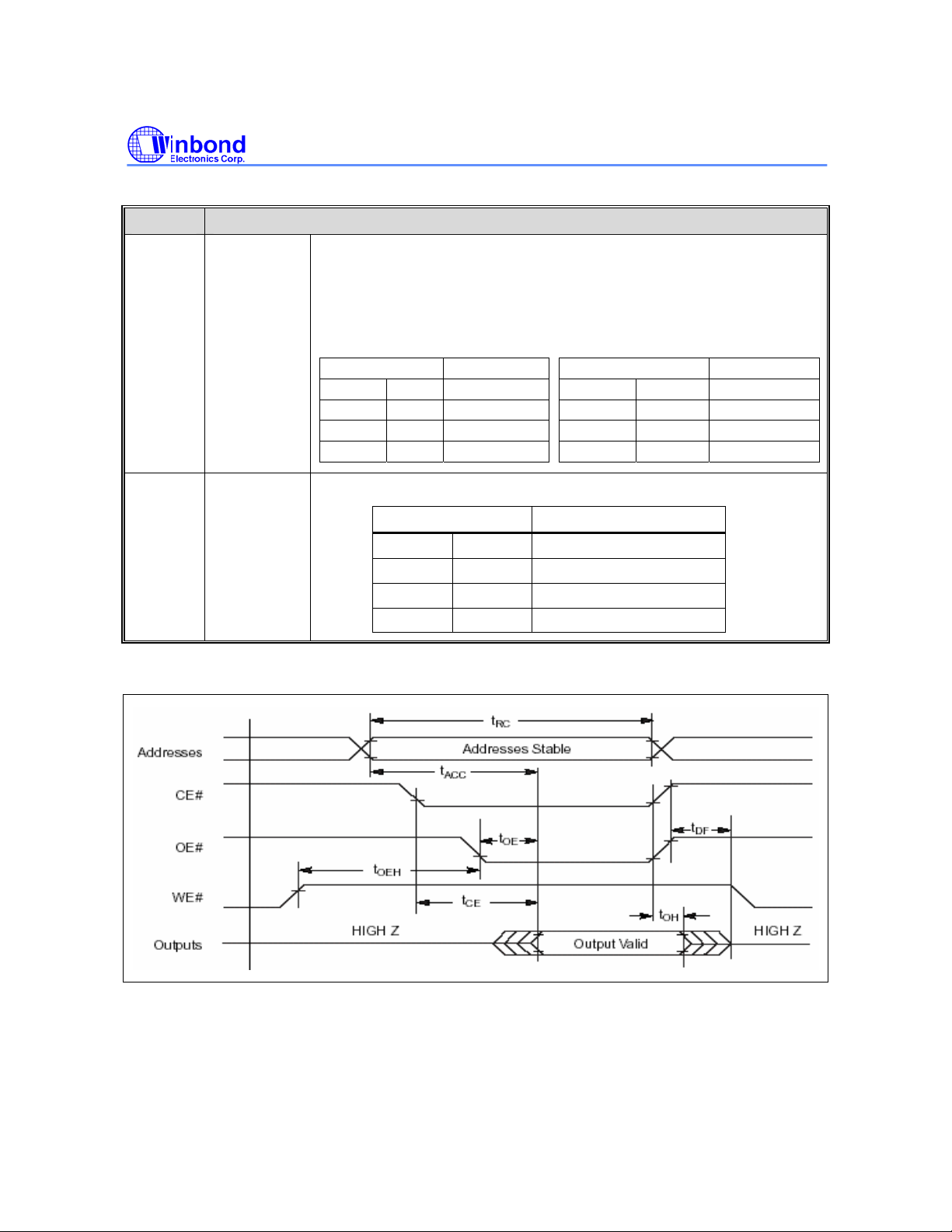
W90P710CD/W90P710CDG
Continued.
BITS DESCRIPTION
Boot ROM/FLASH data bus width
This ROM/Flash bank is designed for a boot ROM. BASADDR bits
determine its start address. The external data bus width is determined by
the data bus signals D [13:12] power-on setting.
[3:2] BTSIZE
[1:0] PGMODE
BTSIZE [3:2] Bus Width D [13:12] Bus Width
0 0 8-bit Pull-down Pull-down 8-bit
0 1 16-bit Pull-down Pull-up 16-bit
1 0 32-bit Pull-up Pull-down 32-bit
1 1 RESERVED Pull-up Pull-up RESERVED
Page mode configuration
PGMODE [1:0] Mode
0 0 Normal ROM
0 1 4 word page
1 0 8 word page
1 1 16 word page
Fig6.3.2 ROM/FLASH Read Operation Timing
Publication Release Date: September 19, 2006
- 73 - Revision B2
Page 74
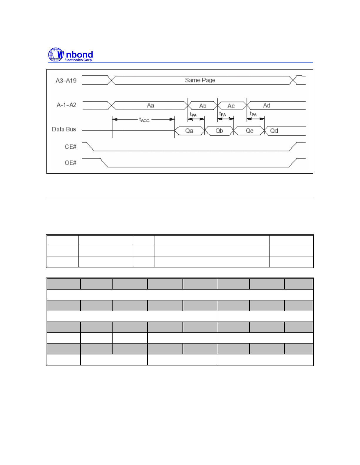
W90P710CD/W90P710CDG
Fig 6.3.3 ROM/FLASH Page Read Operation Timing
Configuration Registers(SDCONF0/1)
The configuration registers enable software to set a number of operating parameters for the SDRAM
controller. There are two configuration registers SDCONF0、SDCONF1 for SDRAM bank 0、bank 1
respectively. Each bank can have a different configuration.
REGISTER ADDRESS R/W DESCRIPTION RESET VALUE
SDCONF0 0xFFF0_1008 R/W SDRAM bank 0 configuration register 0x0000_0800
SDCONF1 0xFFF0_100C R/W SDRAM bank 1 configuration register 0x0000_0800
31 30 29 28 27 26 25 24
BASADDR
23 22 21 20 19 18 17 16
BASADDR RESERVED
15 14 13 12 11 10 9 8
MRSET RESERVED AUTOPR LATENCY RESERVED
7 6 5 4 3 2 1 0
COMPBK DBWD COLUMN SIZE
- 74 -
Page 75
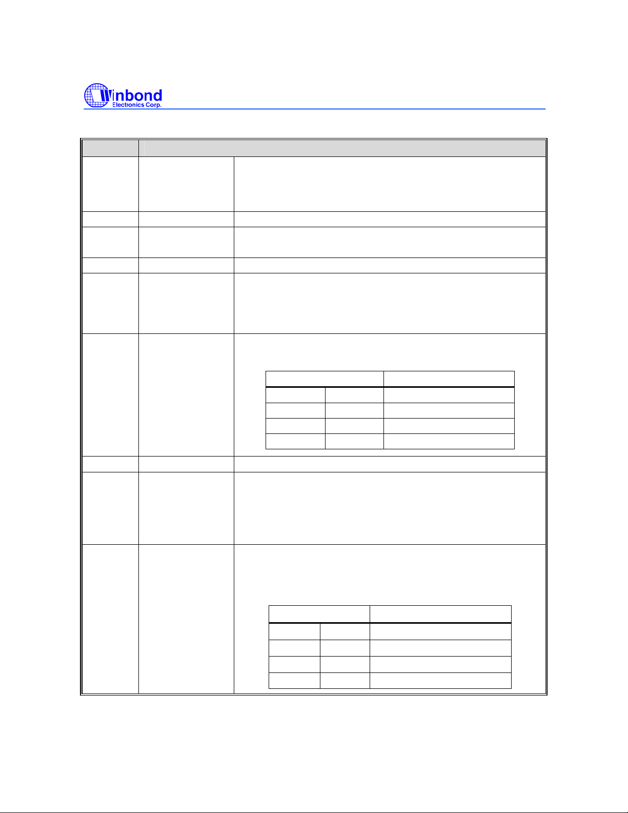
W90P710CD/W90P710CDG
BITS DESCRIPTION
Base address pointer of SDRAM bank 0/1
[31:19] BASADDR
[18:16] RESERVED
[15] MRSET
[14] RESERVED
[13] AUTOPR
[12:11] LATENCY
The start address is calculated as SDRAM bank 0/1 base pointer
<< 18. The SDRAM base address pointer together with the “SIZE”
bits constitutes the whole address range of each SDRAM bank.
-
SDRAM Mode register set command for SDRAM bank 0/1
This bit set will issue a mode register set command to SDRAM.
-
Auto pre-charge mode of SDRAM for SDRAM bank 0/1
Enable the auto pre-charge function of external SDRAM bank 0/1
1= Auto pre-charge
0 = No auto pre-charge
The CAS Latency of SDRAM bank 0/1
Defines the CAS latency of external SDRAM bank 0/1
LATENCY [12:11] MCLK
0 0 1
0 1 2
1 0 3
1 1 REVERSED
[10:8] RESERVED
[7] COMPBK
[6:5] DBWD
-
Number of component bank in SDRAM bank 0/1
Indicates the number of component bank (2 or 4 banks) in external
SDRAM bank 0/1.
0 = 2 banks
1 = 4 banks
Data bus width for SDRAM bank 0/1
Indicates the external data bus width connect with SDRAM bank 0/1
If DBWD = 00, the assigned SDRAM access signal is not generated
i.e. disable.
DBWD [6:5] Bits
0 0 Bank disable
0 1 8-bit (byte)
1 0 16-bit (half-word)
1 1 32-bit (word)
Publication Release Date: September 19, 2006
- 75 - Revision B2
Page 76
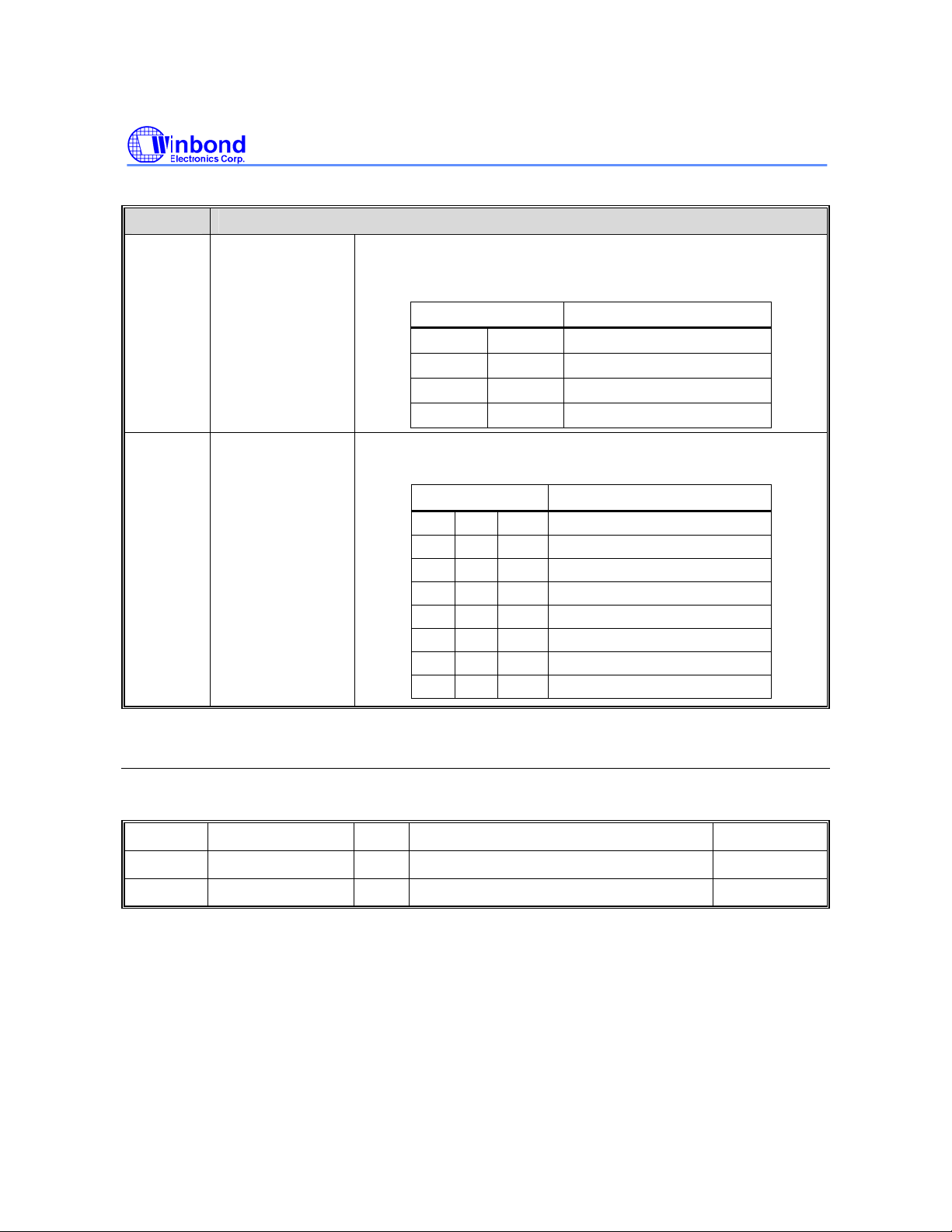
W90P710CD/W90P710CDG
Continued.
BITS DESCRIPTION
Number of column address bits in SDRAM bank 0/1
Indicates the number of column address bits in external SDRAM
bank 0/1.
COLUMN [4:3] Bits
[4:3] COLUMN
Size of SDRAM bank 0/1
Indicates the memory size of external SDRAM bank 0/1
[2:0] SIZE
0 0 8
0 1 9
1 0 10
1 1 REVERSED
SIZE [2:0] Size of SDRAM (Byte)
0 0 0 Bank disable
0 0 1 2M
0 1 0 4M
0 1 1 8M
1 0 0 16M
1 0 1 32M
1 1 0 64M
1 1 1 REVERSED
Timing Control Registers (SDTIME0/1)
W90P710 offers the flexible timing control registers to control the generation and processing of the
control signals and can achieve you use different speed of SDRAM
REGISTER ADDRESS R/W DESCRIPTION RESET VALUE
SDTIME0 0xFFF0_1010 R/W SDRAM bank 0 timing control register
SDTIME1
0xFFF0_1014
R/W SDRAM bank 1 timing control register
- 76 -
0x0000_0000
0x0000_0000
Page 77
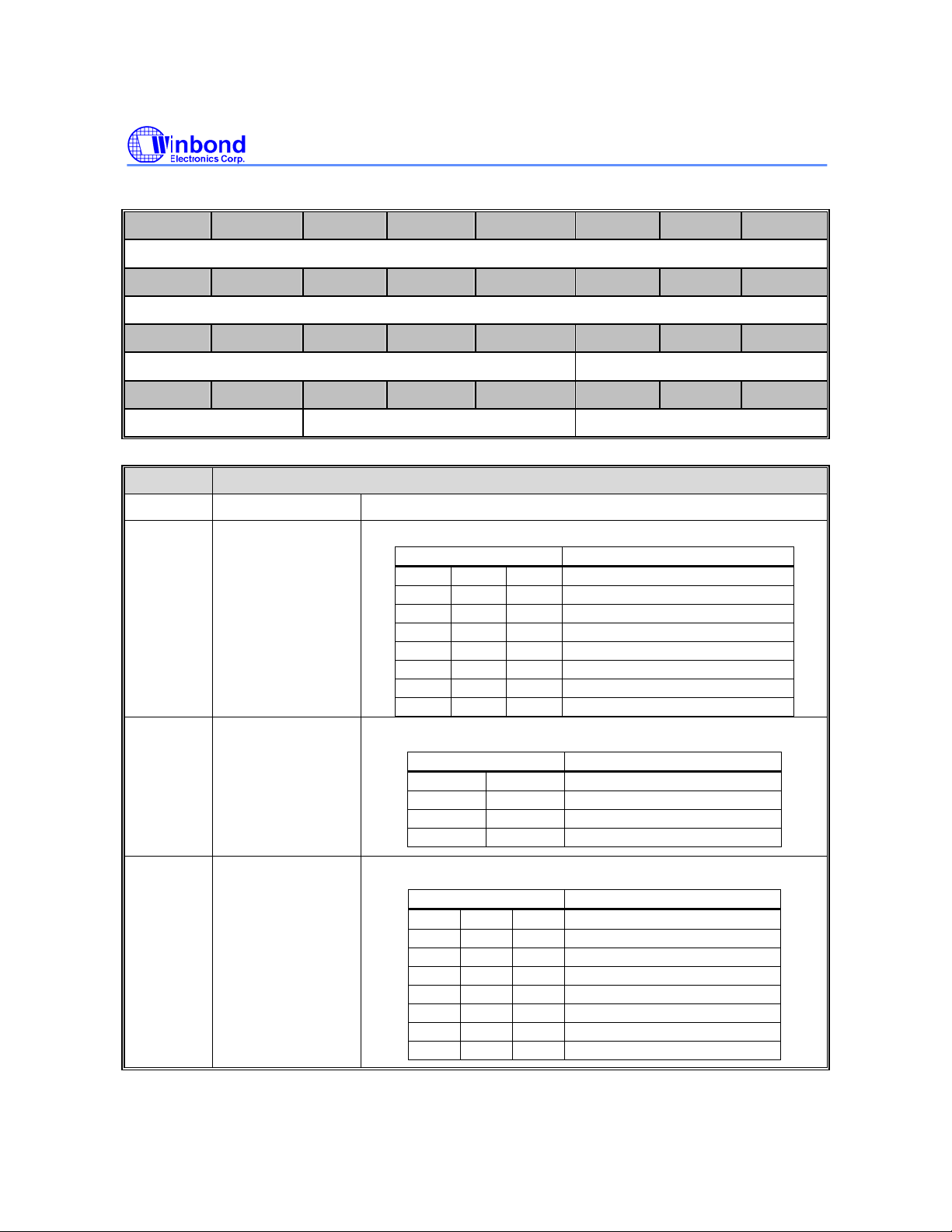
W90P710CD/W90P710CDG
31 30 29 28 27 26 25 24
RESERVED
23 22 21 20 19 18 17 16
RESERVED
15 14 13 12 11 10 9 8
RESERVED tRCD
7 6 5 4 3 2 1 0
tRDL tRP tRAS
BITS DESCRIPTION
[31:11] RESERVED -
SDRAM bank 0/1, /RAS to /CAS delay
tRCD [10:8] MCLK
0 0 0 1
0 0 1 2
[10:8] tRCD
0 1 0 3
0 1 1 4
1 0 0 5
1 0 1 6
1 1 0 7
1 1 1 8
SDRAM bank 0/1, Last data in to pre-charge command
[7:6] tRDL
SDRAM bank 0/1, Row pre-charge time
[5:3] tRP
tRDL [7:6] MCLK
0 0 1
0 1 2
1 0 3
1 1 4
tRP [5:3] MCLK
0 0 0 1
0 0 1 2
0 1 0 3
0 1 1 4
1 0 0 5
1 0 1 6
1 1 0 7
1 1 1 8
Publication Release Date: September 19, 2006
- 77 - Revision B2
Page 78
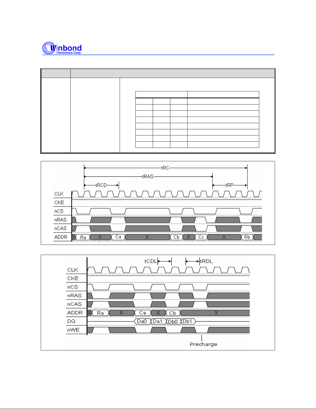
W90P710CD/W90P710CDG
Continued.
BITS DESCRIPTION
SDRAM bank 0/1, Row active time
tRAS [2:0] MCLK
0 0 0 1
0 0 1 2
[2:0] tRAS
0 1 0 3
0 1 1 4
1 0 0 5
1 0 1 6
1 1 0 7
1 1 1 8
Fig 6.3.4 Access timing 1 of SDRAM
Fig 6.3.5 Access timing 2 of SDRAM
- 78 -
Page 79
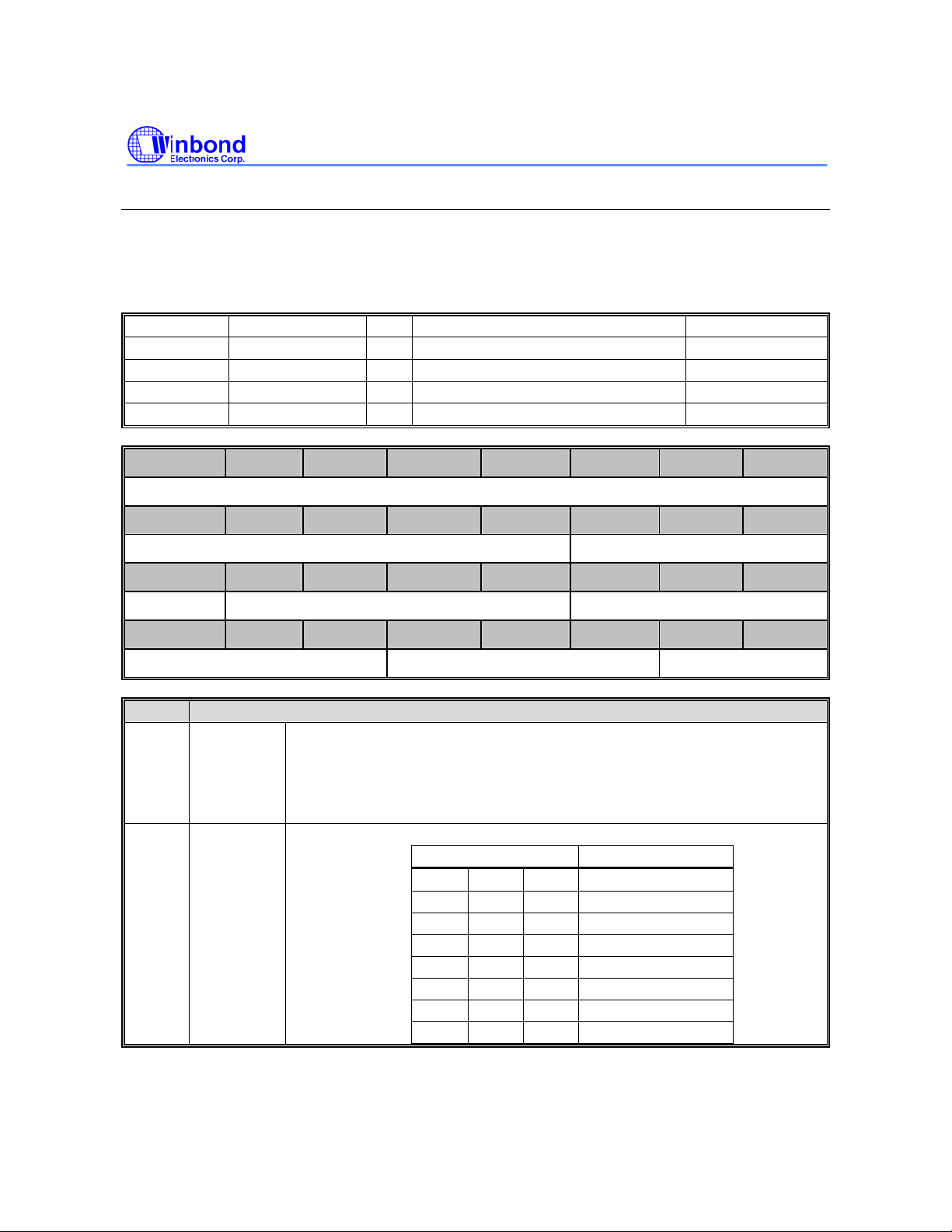
W90P710CD/W90P710CDG
External I/O Control Registers(EXT0CON – EXT3CON)
The W90P710 supports an external device control without glue logic. It is very cost effective because
address decoding and control signals timing logic are not needed. Using these control registers you can
configure special external I/O devices for providing the low cost external devices control solution.
REGISTER ADDRESS R/W DESCRIPTION RESET VALUE
EXT0CON 0xFFF0_1018 R/W External I/O 0 control register 0x0000_0000
EXT1CON 0xFFF0_101C R/W External I/O 1 control register 0x0000_0000
EXT2CON 0xFFF0_1020 R/W External I/O 2 control register 0x0000_0000
EXT3CON 0xFFF0_1024 R/W External I/O 3 control register 0x0000_0000
31 30 29 28 27 26 25 24
BASADDR
23 22 21 20 19 18 17 16
BASADDR SIZE
15 14 13 12 11 10 9 8
ADRS tACC tCOH
7 6 5 4 3 2 1 0
tACS tCOS DBWD
BITS DESCRIPTION
Base address pointer of external I/O bank 0~3
The start address of each external I/O bank is calculated as “BASADDR”
[31:11] BASADDR
[18:16] SIZE
base pointer << 18.
Each external I/O bank base address pointer together with the “SIZE” bits
constitutes the whole address range of each external I/O bank.
The size of the external I/O bank 0~3
SIZE [18:16] Byte
0 0 0 256K
0 0 1 512K
0 1 0 1M
0 1 1 2M
1 0 0 4M
1 0 1 8M
1 1 0 16M
1 1 1 REVERSED
Publication Release Date: September 19, 2006
- 79 - Revision B2
Page 80
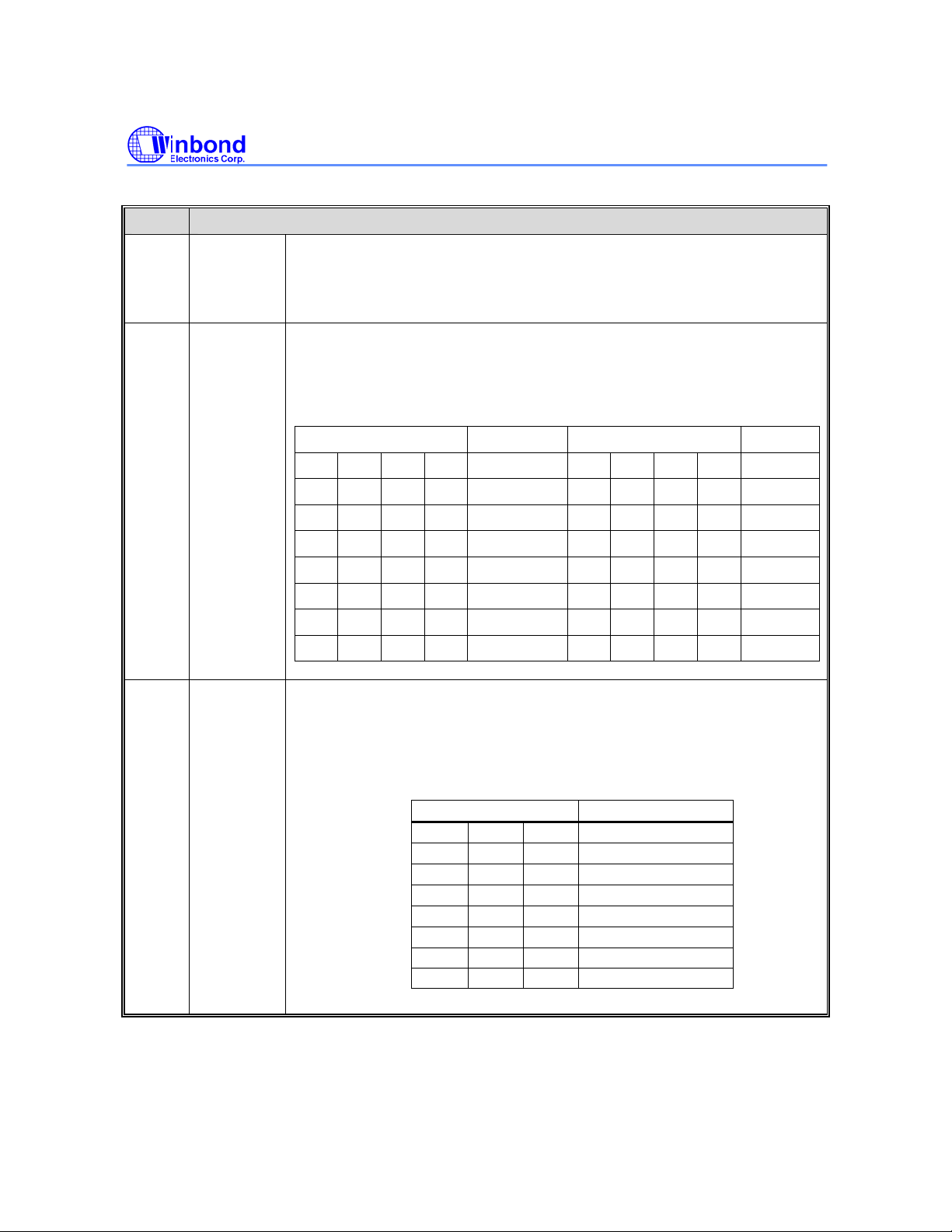
W90P710CD/W90P710CDG
Continued.
BITS DESCRIPTION
Address bus alignment for external I/O bank 0~3
[15] ADRS
[14:11] tACC
When ADRS is set, external address (A21~A0) bus is alignment to byte
address format, that is, A0 is internal AHB address bus HADDR[0] and A1 is
AHB bus HADDR[1] and so forth. And it ignores DBWD [1:0] setting.
Access cycles of external I/O bank 0~3
This parameter means nWE, nWBE and nOE active time clock. Detail timing
diagram please refer to Fig. 6.3.6 and 6.3.7
tACC[14:11] MCLK tACC[14:11] MCLK
0 0 0 0 Reversed 1 0 0 0 9
0 0 0 1 1 1 0 0 1 11
0 0 1 0 2 1 0 1 0 13
0 0 1 1 3 1 0 1 1 15
0 1 0 0 4 1 1 0 0 17
0 1 0 1 5 1 1 0 1 19
0 1 1 0 6 1 1 1 0 21
0 1 1 1 7 1 1 1 1 23
[10:8] tCOH
Chip selection hold time of external I/O bank 0~3
This parameters control nWBE and nOE hold time. Detail timing diagram
please refer to Fig. 6.3.6 and 6.3.7
tCOH [10:8] MCLK
0 0 0 0
0 0 1 1
0 1 0 2
0 1 1 3
1 0 0 4
1 0 1 5
1 1 0 6
1 1 1 7
- 80 -
Page 81
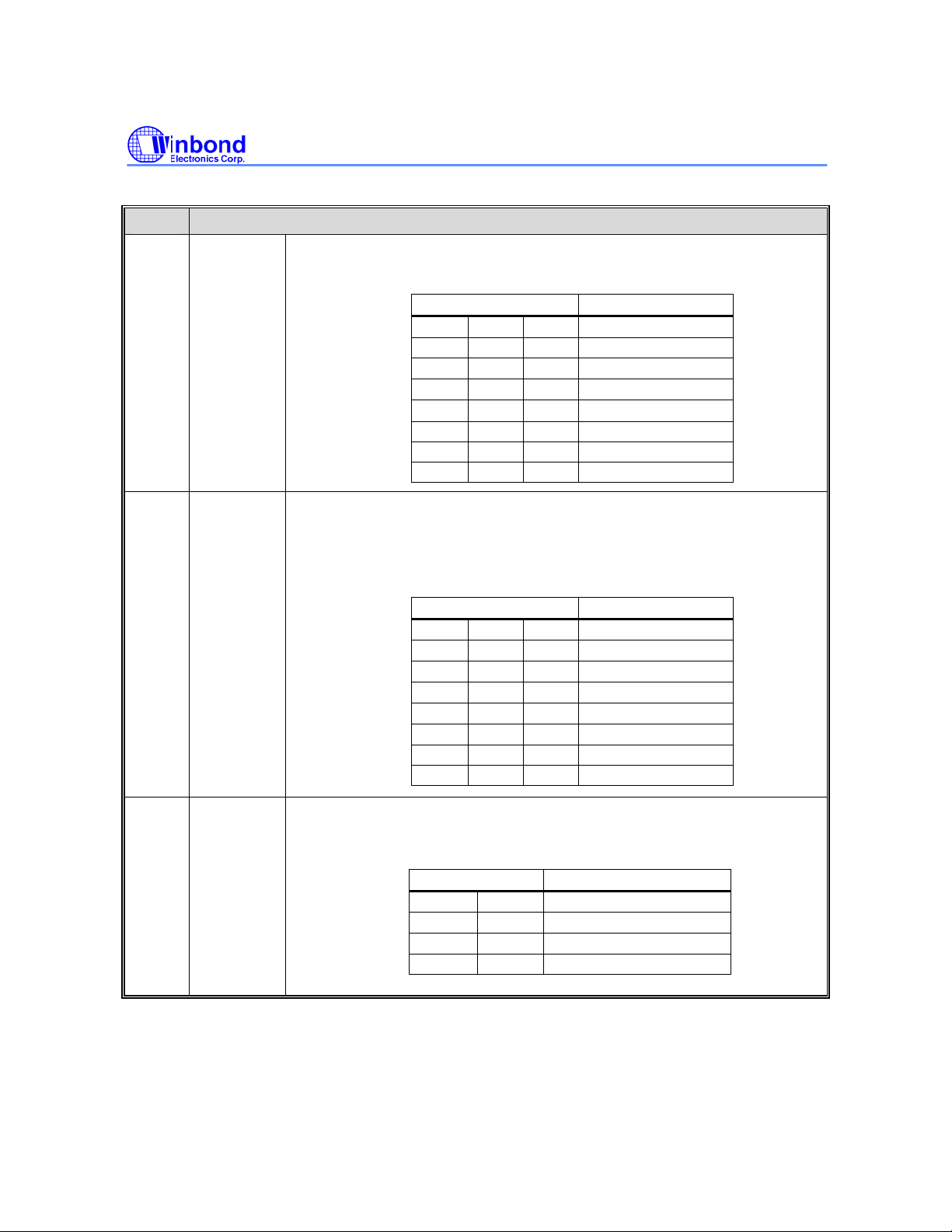
W90P710CD/W90P710CDG
Continued.
BITS DESCRIPTION
Address set-up before nECS for external I/O bank 0~3
tACS [7:5] MCLK
0 0 0 0
0 0 1 1
[7:5] tACS
Chip selection set-up time of external I/O bank 0~3
When ROM/Flash memory bank is configured, the access to its bank
stretches chip selection time before the nOE or new signal is activated.
[4:2] tCOS
0 1 0 2
0 1 1 3
1 0 0 4
1 0 1 5
1 1 0 6
1 1 1 7
tCOS [4:2] MCLK
0 0 0 0
0 0 1 1
0 1 0 2
0 1 1 3
1 0 0 4
1 0 1 5
1 1 0 6
1 1 1 7
[1:0] DBWD
Programmable data bus width for external I/O bank 0~3
DBWD [1:0] Width of Data Bus
0 0 Disable bus
0 1 8-bit
1 0 16-bit
1 1 32-bit
Publication Release Date: September 19, 2006
- 81 - Revision B2
Page 82
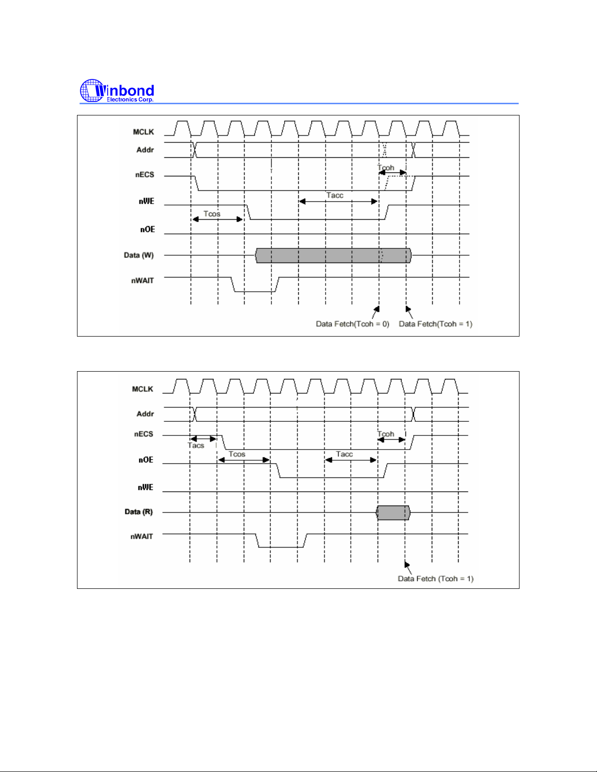
W90P710CD/W90P710CDG
Fig 6.3.6 External I/O write operation timing
Fig 6.3.7 External I/O read operation timing
- 82 -
Page 83
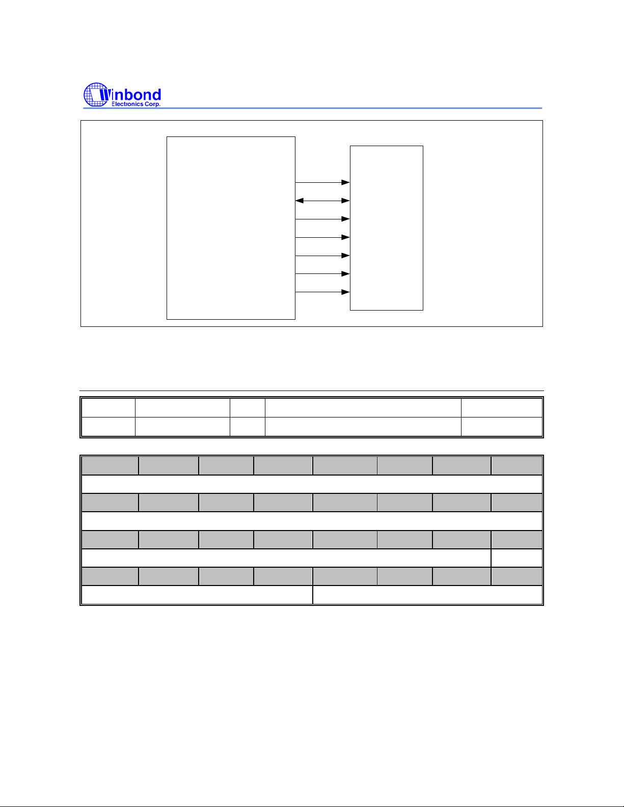
W90P710
W90P710CD/W90P710CDG
2Mx16 SRAM
A[21:0]
D[31:0]
nECSn
nWE
nOE
nWBE_SDQM[1]
nWBE_SDQM[0]
Fig. 6.3.8 External IO bank with 16-bit SRAM
A[21:0]
DQ[15:0]
nCS
nWE
nOE
nUB
nLB
Clock Skew Control Register (CKSKEW)
Register Address R/W Description Reset Value
CKSKEW
31 30 29 28 27 26 25 24
0xFFF0_1F00
R/W Clock skew control register 0xXXXX_0018
DLH_CLK_REF
23 22 21 20 19 18 17 16
DLH_CLK_REF
15 14 13 12 11 10 9 8
RESVERED SWPON
7 6 5 4 3 2 1 0
DLH_CLK_SKEW MCLK_O_D
Publication Release Date: September 19, 2006
- 83 - Revision B2
Page 84
W90P710CD/W90P710CDG
BITS DESCRIPTION
Latch DLH_CLK clock tree by HCLK positive edge
[31:16] DLH_CLK_REF
[15:9] RESERVED -
[8] SWPON
The SDRAM MCLK is generated by inserting a delay (XOR2) chain in
HCLK positive or negedge edge to adjust the MCLK skew. So software
can read these bits to expore MCLK and HCLK relationship. [31:24] is
used for positive edge and [23:16] is for negedge edge.
SDRAM Initialization by Software
Set this bit “1” will issue a SDRAM power on default setting command
sequence like system power on, this bit will be auto-clear by hardware
while SDRAM initialization finish.
Data latch Clock Skew Adjustment
Due to PC board loading or too many devices connect to external
address and data bus, it may causes SDRAM can not work correctly at
high frequency (usually, > 80MHz) software can control
MCLK_O_D[3:0] to adjust address and data bus to adjust setup/hold
time.
DLH_CLK_SKEW[7:4] Gate
Delay
DLH_CLK_SKEW[7:4] Gate
Delay
[7:4] DLH_CLK_SKEW
0 0 0 0 P-0 1 0 0 0 N-0
0 0 0 1 P-1 1 0 0 1 N-1
0 0 1 0 P-2 1 0 1 0 N-2
0 0 1 1 P-3 1 0 1 1 N-3
0 1 0 0 P-4 1 1 0 0 N-4
0 1 0 1 P-5 1 1 0 1 N-5
0 1 1 0 P-6 1 1 1 0 N-6
0 1 1 1 P-7 1 1 1 1 N-7
NOTE: P-x means Data latched Clock shift “X” gates delays by refer
MCLKO positive edge, N-x means Data latched Clock shift “X” gates
delays by refer MCLKO negative edge.
- 84 -
Page 85
W90P710CD/W90P710CDG
Continued.
BITS DESCRIPTION
MCLK output delay adjustment
MCLK_O_D [3:0] Gate
0 0 0 0 P-0 1 0 0 0 N-0
0 0 0 1 P-1 1 0 0 1 N-1
0 0 1 0 P-2 1 0 1 0 N-2
0 0 1 1 P-3 1 0 1 1 N-3
[3:0] MCLK_O_D
0 1 0 0 P-4 1 1 0 0 N-4
0 1 0 1 P-5 1 1 0 1 N-5
0 1 1 0 P-6 1 1 1 0 N-6
0 1 1 1 P-7 1 1 1 1 N-7
NOTE: “P-x” means MCLKO shift “X” gates delay by refer HCLK
positive edge, “N-x” means MCLKO shift “X” gates delay by refer HCLK
negative edge. MCLK is the output pin of MCLKO, which is an internal
signal on chip.
Delay
MCLK_O_D [3:0] Gate
Delay
Publication Release Date: September 19, 2006
- 85 - Revision B2
Page 86
W90P710CD/W90P710CDG
6.4 Cache Controller
The W90P710 incorporates a 4KB Instruction cache, 4KB Data cache and 8 words write buffer. The ICache and D-Cache have similar organization except the cache size. To raise the cache-hit ratio, these
two caches are configured two-way set associative addressing. Each cache has four words cache line
size. When a miss occurs, four words must be fetched consecutively from external memory. The
replacement algorithm is a LRU (Least Recently Used).
If disabling the I-Cache / D-Cache, these cache memories can be treated as On-Chip RAM. The
W90P710 also provides a write buffer to improve system performance. The write buffer can buffer up to
eight words of data.
6.4.1 On-Chip RAM
If I-Cache or D-Cache is disabled, it can be served as On-Chip RAM. If D-Cache is disabled, there has
4KB On-Chip RAM, its start address is 0xFFE01000. If I-Cache is disabled, there has 4KB On-Chip RAM
and the start address of this RAM is 0xFFE00000. If both the I-Cache and D-Cache are disabled, it has
8KB On-Chip RAM starting from 0xFFE00000.
The size of On-Chip RAM is depended on the I-Cache and D-Cache enable bits ICAEN, DCAEN in
Cache Control Register (CAHCON).
Table6.4.1 The size and start address of On-Chip RAM
ICAEN DCAEN
SIZE START ADDRESS
0 0 8KB 0xFFE0_0000
0 1 4KB 0xFFE0_0000
1 0 4KB 0xFFE0.1000
1 1 Unavailable
ON-CHIP RAM
6.4.2 Non-Cacheable Area
Although the cache affects the entire 2GB system memory, it is sometimes necessary to define noncacheable areas when the consistency of data stored in memory and the cache must be ensured. To
support this, the W90P710 provides a non-cacheable area control bit in the address field, A[31].
If A[31] in the ROM/FLASH, SDRAM, or external I/O bank’s access address is “0”, then the accessed
data is cacheable. If the A [31] value is “1”, the accessed data is non-cacheable.
- 86 -
Page 87

W90P710CD/W90P710CDG
6.4.3 Instruction Cache
The Instruction cache (I-cache) is a 4K bytes two-way set associative cache. The cache organization is
128 sets, two lines per set, and four words per line. Cache lines are aligned on 4-word boundaries in
memory. The cache access cycle begins with an instruction request from the instruction unit in the core.
In the case of a cache hit, the instruction is delivered to the instruction unit. In case of a cache miss, the
cache initiates a burst read cycle on the internal bus with the address of the requested instruction. The
first word received from the bus is the requested instruction. The cache forwards this instruction to the
instruction unit of the core as soon as it is received from the internal bus. A cache line is then selected to
receive the data that will be coming from the bus. A least recently used (LRU) replacement algorithm is
used to select a line when no empty lines are available. When I-Cache is disabled, the cache memory is
served as 4KB On-chip RAM. The I-Cache is always disabled on reset.
The following is a list of the instruction cache features:
y 4K bytes instruction cache
y Two-way set associative
y Four words in a cache line
y LRU replacement policy
y Lockable on a per-line basis
y Critical word first, burst access
Instruction Cache Operation
On an instruction fetch, bits 10-4 of the instruction’s address point into the cache to retrieve the tags and
data of one set. The tags from both ways are then compared against bits 30-11 of the instruction’s
address. If a match is found and the matched entry is valid, then it is a cache hit. If neither tags match nor
the matched tag is not valid, it is a cache miss.
Instruction Cache Hit
In case of a cache hit, bits 3-2 of the instruction address is used to select one word from the cache line
whose tag matches. The instruction is immediately transferred to the instruction unit of the core.
Instruction Cache Miss
On an instruction cache miss, the address of the missed instruction is driven on the internal bus with a 4word burst transfer read request. A cache line is then selected to receive the data that will be coming
from the bus. The selection algorithm gives first priority to invalid lines. If neither of the two lines in the
selected set is invalid, then the least recently used line is selected for replacement. Locked lines are
never replaced. The transfer begins with the word requested by the instruction unit (critical word first),
followed by the remaining words of the line, then by the word at the beginning of the lines (wraparound).
Instruction Cache Flushing
The W90P710 does not support external memory snooping. Therefore, if self-modifying code is written,
the instructions in the I-Cache may become invalid. The entire I-Cache can be flushed by software in one
operation, or can be flushed one line at a time by setting the CAHCON register bit FLHS or FLHA with
the ICAH bit is set. As flushing the cache line, the “V” bit of the line is cleared to “0”. The I-Cache is
automatically flushed during reset.
Publication Release Date: September 19, 2006
- 87 - Revision B2
Page 88

W90P710CD/W90P710CDG
Instruction Cache Load and Lock
The W90P710 supports a cache-locking feature that can be used to lock critical sections of code into ICache to guarantee quick access. Lockdown can be performed with a granularity of one cache line. The
smallest space, which can be locked down, is 4 words. After a line is locked, it operates as a regular
instruction SRAM. Lines locked are not replaced during misses and not affected by flush per line
command.
To load and lock instruction, the following sequence should be followed:
1. Write the start address of the instructions to be locked into CAHADR register.
2. Set LDLK and ICAH bits in the CAHCON register.
3. Increased the address by 16 and written into CAHADR register.
4. Set LDLK and ICAH bits in the CAHCON register.
5. Repeat the steps 3 and 4, until the desired instructions are all locked.
When using I-Cache load and lock command, there are some notes should be cared.
y The programs executing load and lock operation should be held in a non-cacheable area of
memory.
y The cache should be enabled and interrupts should be disabled.
y Software must flush the cache before execute load and lock to ensure that the code to be locked
down is not already in the cache.
Instruction Cache Unlock
The unlock operation is used to unlock previously locked cache lines. After unlock, the “L” bit of the line
is cleared to “0”. W90P710 has two unlock command, unlock line and unlock all.
The unlock line operation is performed on a cache line granularity. In case the line is found in the cache,
it is unlocked and starts to operate as a regular valid cache line. In case the line is not found in the
cache, no operation is done and the command terminates with no exception. To unlock one line the
following unlock line sequence should be followed:
1. Write the address of the line to be unlocked into the CAHADR Register.
2. Set the ULKS and ICAH bits in the CAHCON register.
The unlock all operation is used to unlock the whole I-Cache. This operation is performed on all cache
lines. In case a line is locked, it is unlocked and starts to operate as regular valid cache line. In case a
line is not locked or if it is invalid, no operation is performed. To unlock the whole cache, set the ULKA
and ICAH bits.
- 88 -
Page 89

W90P710CD/W90P710CDG
6.4.4 Data Cache
The W90P710 data cache (D-Cache) is a 4KB two-way set associative cache. The cache organization is
128 sets, two lines per set, and four words per line. Cache lines are aligned on 4-word boundaries in
memory. The cache is designed for buffer write-through mode of operation and a least recently used
(LRU) replacement algorithm is used to select a line when no empty lines are available.
When D-Cache is disabled, the cache memory is served as 4KB On-chip RAM.
The D-Cache is always disabled on reset.
The following is a list of the data cache features:
y 4K bytes data cache
y Two-way set associative
y Four words in a cache line
y LRU replacement policy
y Lockable on a per-line basis
y Critical word first, burst access
y Buffer Write-through mode
y 8 words write buffer
y Drain write buffer
Data Cache Operation
On a data fetch, bits 10-4 of the data’s address point into the cache to retrieve the tags and data of one
set. The tags from both ways are then compared against bits 30-11 of the data’s address. If a match is
found and the matched entry is valid, then it is a cache hit. If neither tags match nor the matched tag is
not valid, it is a cache miss.
Data Cache Read
Read Hit:On a cache hit, the requested word is immediately transferred to the core.
Read Miss:A line in the cache is selected to hold the data, which will be fetched from memory. The
selection algorithm gives first priority to invalid lines and if both lines are invalid the line in way zero is
selected first. If neither of the two candidate lines in the selected set is invalid, then one of the lines is
selected by the LRU algorithm to replace. The transfer begins with the aligned word containing the
missed data (critical word first), followed by the remaining word in the line, then by the word at the
beginning of the line (wraparound). As the missed word is received from the bus, it is delivered directly to
the core.
Data Cache Write
As buffer write-through mode, store operations always update memory. The buffer write-through mode is
used when external memory and internal cache images must always agree.
Publication Release Date: September 19, 2006
- 89 - Revision B2
Page 90

W90P710CD/W90P710CDG
Write Hit:Data is written into both the cache and write buffer. The processor then continues to access
the cache, while the cache controller simultaneously downloads the contents of the write buffer to main
memory. This reduces the effective write memory cycle time from the time required for a main memory
cycle to the cycle time of the high-speed cache.
Write Miss:Data is only written into write buffer, not to the cache (write no allocate).
Data Cache Flushing
The W90P710 allows flushing of the data cache under software control. The data cache may be
invalidated through writing flush line (FLHS) or flush all (FLHA) commands to the CAHCON register.
Flushing the entire D-Cache also flushed any locked down code. As flushing the data cache, the “V” bit
of the line is cleared to “0”. The D-cache is automatically flushed during reset.
Data Cache Load and Lock
The W90P710 supports a cache-locking feature that can be used to lock critical sections of data into DCache to guarantee quick access. Lockdown can be performed with a granularity of one cache line. The
smallest space, which can be locked down, is 4 words. After a line is locked, it operates as a regular
instruction SRAM. The locked lines are not replaced during misses and it is not affected by flush per line
command.
To load and lock data, the following sequence should be followed:
1. Write the start address of the data to be locked into CAHADR register.
2. Set LDLK and DCAH bits in the CAHCON register.
3. Increased the address by 16 and written into CAHADR register.
4. Set LDLK and DCAH bits in the CAHCON register.
5. Repeat the steps 3 and 4, until the desired data are all locked.
When using D-Cache load and lock command, there are some notes should be cared.
y The programs executing load and lock operation should be held in a non-cacheable area of
memory.
y The cache should be enabled and interrupts should be disabled.
y Software must flush the cache before execute load and lock to ensure that the data to be locked
down is not already in the cache.
Data Cache Unlock
The unlock operation is used to unlock previously locked cache lines. After unlock, the “L” bit of the line
is cleared to “0”. W90P710 has two unlock command, unlock line and unlock all.
The unlock line operation is performed on a cache line granularity. In case the line is found in the cache,
it is unlocked and starts to operate as a regular valid cache line. In case the line is not found in the
cache, no operation is done and the command terminates with no exception. To unlock one line the
following unlock line sequence should be followed:
1. Write the address of the line to be unlocked into the CAHADR Register.
2. Set the ULKS and DCAH bits in the CAHCON register.
- 90 -
Page 91
W90P710CD/W90P710CDG
The unlock all operation is used to unlock the whole D-Cache. This operation is performed on all cache
lines. In case a line is locked, it is unlocked and starts to operate as regular valid cache line. In case a
line is not locked or if it is invalid, no operation is performed. To unlock the whole cache, set the ULKA
and DCAH bits.
6.4.5 Write Buffer
The W90P710 provides a write buffer to improve system performance. The write buffer can buffer up to
eight words of data. The write buffer may be enabled or be disabled via the WRBEN bit in the CAHCNF
register, and the buffer is disabled and flushed on reset.
Drain write buffer
To force data, this is in write buffer, to be written to external main memory. This operation is useful in real
time applications where the processor needs to be sure that a write to a peripheral has completed before
program execution continues.
To perform this command, you can set the DRWB and DCAH bits in CAHCON register.
6.4.6 Cache Control Registers Map
REGISTER ADDRESS R/W DESCRIPTION RESET VALUE
CAHCNF
CAHCON
0xFFF0_2000
0xFFF0_2004
R/W Cache configuration register 0x0000_0000
R/W Cache control register
0x0000_0000
CAHADR 0xFFF0_2008 R/W Cache address register 0x0000_0000
CTEST0
CTEST1
0xFFF6_0000
0xFFF6_0004
R/W Cache test register 0 0x0000_0000
R Cache test register 1
0x0000_0000
Configuration Register (CAHCNF)
Cache controller has a configuration register to enable or disable the I-Cache, D-Cache, and Write
buffer.
REGISTER ADDRESS R/W DESCRIPTION RESET VALUE
CAHCNF
0xFFF0_2000
R/W Cache configuration register 0x0000_0000
Publication Release Date: September 19, 2006
- 91 - Revision B2
Page 92
W90P710CD/W90P710CDG
31 30 29 28 27 26 25 24
RESERVED
23 22 21 20 19 18 17 16
RESERVED
15 14 13 12 11 10 9 8
RESERVED
7 6 5 4 3 2 1 0
RESERVED WRBEN DCAEN ICAEN
BITS DESCRIPTION
[31:3] RESERVED
[2] WRBEN
-
Write buffer enable
Write buffer is disabled after reset.
1 = Enable write buffer
0 = Disable write buffer
D-Cache enable
[1] DCAEN
[0] ICAEN
D-Cache is disabled after reset.
1 = Enable D-cache
0 = Disable D-cache
I-Cache enable
I-Cache is disabled after reset.
1 = Enable I-cache
0 = Disable I-cache
Control Register (CAHCON)
Cache controller supports one Control register used to control the following operations.
y Flush I-Cache and D-Cache
y Load and lock I-Cache and D-Cache
y Unlock I-Cache and D-Cache
y Drain write buffer
These command set bits in CAHCON register are auto-clear bits. As the end of execution, that command
set bit will be cleared to “0” automatically.
- 92 -
Page 93
W90P710CD/W90P710CDG
REGISTER ADDRESS R/W DESCRIPTION RESET VALUE
CAHCON
31 30 29 28 27 26 25 24
23 22 21 20 19 18 17 16
15 14 13 12 11 10 9 8
7 6 5 4 3 2 1 0
DRWB ULKS ULKA LDLK FLHS FLHA DCAH ICAH
BITS DESCRIPTION
[31:8] RESERVED
[7] DRWB
[6] ULKS
[5] ULKA
[4] LDLK
[3] FLHS
[2] FLHA
[1] DCAH
[0] ICAH
0xFFF0_2004
R/W Cache control register
RESERVED
RESERVED
RESERVED
-
Drain write buffer
Forces write buffer data to be written to main memory.
Unlock I-Cache/D-Cache single line
Unlocks the I-Cache/D-Cache per line. Both WAY and ADDR bits in
CAHADR register must be specified.
Unlock I-Cache/D-Cache entirely
Unlocks the entire I-Cache/D-Cache, the lock bit “L” will be cleared
to 0.
Load and Lock I-Cache/D-Cache
Loads the instruction or data from external memory and locks into
cache. Both WAY and ADDR bits in CAHADR register must be
specified.
Flush I-Cache/D-Cache single line
Flushes the entire I-Cache/D-Cache per line. Both WAY and ADDR
bits in CAHADR register must be specified.
Flush I-Cache/D-Cache entirely
To flush the entire I-Cache/D-Cache, also flushes any locked-down
code. If the I-Cache/D-Cache contains locked down code, the
programmer must flush lines individually
D-Cache selected
When set to “1”, the command set is executed with D-Cache.
I-Cache selected
When set to “1”, the command set is executed with I-Cache.
0x0000_0000
Publication Release Date: September 19, 2006
- 93 - Revision B2
Page 94
W90P710CD/W90P710CDG
NOTE:When using the FLHA or ULKA command, you can set both ICAH and DCAH bits to execute
entire I-Cache and D-Cache flushing or unlocking. But, FLHS and ULKS commands can only be
executed with a cache line specified by CAHADR register in I-Cache or D-Cache at a time. If you set
both ICAH and DCAH bits, and set FLHS or ULKS command bit, it will be treated as an invalid
command and no operation is done and the command terminates with no exception.
The Drain Write Buffer operation is only for D-Cache. To perform this operation, you must set DRWB
and DCAH bits. If the ICAH bit is set when using DRWB command, it will be an invalid command and no
operation is done and the command terminates with no exception.
Address Register (CAHADR)
W90P710 Cache Controller supports one address register. This address register is used with the
command set in the control register (CAHCON) by specifying instruction/data address.
REGISTER ADDRESS R/W DESCRIPTION RESET VALUE
CAHADR 0xFFF0_2008 R/W Cache address register 0x0000_0000
31 30 29 28 27 26 25 24
WAY ADDR
23 22 21 20 19 18 17 16
ADDR
15 14 13 12 11 10 9 8
ADDR
7 6 5 4 3 2 1 0
ADDR
BITS DESCRIPTION
Way selection
[31] WAY
[30:0] ADDR The absolute address of instruction or data
0 = Way0 is selected
1 = Way1 is selected
- 94 -
Page 95
W90P710CD/W90P710CDG
Cache Test Register 0 (CTEST0)
Cache test control register that configures the cache and tag ram testing enable or disable. In addition,
this register controls the built-in-self-test (BIST) function of SRAM.
REGISTER ADDRESS R/W DESCRIPTION RESET VALUE
CTEST0 0xFFF6_0000 R/W Cache test register 0 0x0000_0000
31 30 29 28 27 26 25 24
RESERVED
23 22 21 20 19 18 17 16
RESERVED
15 14 13 12 11 10 9 8
BISTEN RESERVED BST_GP3 BST_GP2 BST_GP1 BST_GP0
7 6 5 4 3 2 1 0
RESERVED CATEST
BITS DESCRIPTION
[31:16] RESERVED
[15] BISTEN
[14:12] RESERVED
[11] BIST_GP3
[10] BIST_GP2
[9] BIST_GP1
[8] BIST_GP0
[7:0] RESERVED
-
BIST mode enable
When set to “1”, BIST mode will be enabled, the selected memory
groups begins to be tested by BIST.
-
Memory group 3 is selected to test by BIST
When set to “1”, memory group 3, including data cache tag ram
way 0 and way 1, are selected to be tested by BIST.
Memory group 2 is selected to test by BIST
When set to “1”, memory group 2, including program cache tag
ram way 0 and way 1, are selected to be tested by BIST.
Memory group 1 is selected to test by BIST
When set to “1”, memory group 1, including data cache ram way 0
and way 1, are selected to be tested by BIST.
Memory group 0 is selected to test by BIST
When set to “1”, memory group 0, including program cache ram
way 0 and way 1, are selected to be tested by BIST.
-
** Note: The 4 memory groups can be selected and tested simultaneously by BIST.
Publication Release Date: September 19, 2006
- 95 - Revision B2
Page 96
W90P710CD/W90P710CDG
Cache Test Register 1 (CTEST1)
Cache Test Register that will be read back to provide the status of cache RAM BIST. Whether the BIST
is finish and all of bank of SRAM are tested successfully will be presented in this register.
Register Address R/W Description Reset Value
CTEST1
31 30 29 28 27 26 25 24
FINISH RESERVED
23 22 21 20 19 18 17 16
15 14 13 12 11 10 9 8
7 6 5 4 3 2 1 0
BFAIL7 BFAIL6 BFAIL5 BFAIL4 BFAIL3 BFAIL2 BFAIL1 BFAIL0
BITS DESCRIPTION
[31] FINISH
[30:8] RESERVED
[7] BFAIL7
[6] BFAIL6
[5] BFAIL5
[4] BFAIL4
[3] BFAIL3
0xFFF6_0004
R Cache test register 1
RESERVED
RESERVED
BIST completed
This bit is “0” initially. When BIST mode enabled, this bit will be “1”
after BIST test completed. The values of BFAIL0-7 are valid only
after FINISH = 1.
-
BIST test fail for data cache tag ram way 1
If this bit equals to “1”, it indicates the data cache tag ram for way
1 is tested fail by BIST. “0” means the test is passed.
BIST test fail for data cache tag ram way 0
If this bit equals to “1”, it indicates the data cache tag ram for way
0 is tested fail by BIST. “0” means the test is passed.
BIST test fail for instruction cache tag ram way 1
If this bit equals to “1”, it indicates the instruction cache tag ram for
way 1 is tested fail by BIST. “0” means the test is passed.
BIST test fail for instruction cache tag ram way 0
If this bit equals to “1”, it indicates the instruction cache tag ram for
way 0 is tested fail by BIST. “0” means the test is passed.
BIST test fail for data cache ram way 1
If this bit equals to “1”, it indicates the data cache ram for way 1 is
tested fail by BIST. “0” means the test is passed.
0x0000_0000
- 96 -
Page 97

W90P710CD/W90P710CDG
Continued.
BITS DESCRIPTION
BIST test fail for data cache ram way 0
[2] BFAIL2
[1] BFAIL1
[0] BFAIL0
6.5 Ethernet MAC Controller
If this bit equals to “1”, it indicates the data cache ram for way 0 is
tested fail by BIST. “0” means the test is passed.
BIST test fail for instruction cache ram way 1
If this bit equals to “1”, it indicates the instruction cache ram for
way 1 is tested fail by BIST. “0” means the test is passed.
BIST test fail for instruction cache ram way 0
If this bit equals to “1”, it indicates the instruction cache ram for
way 0 is tested fail by BIST. “0” means the test is passed.
Overview
The W90P710 provides an Ethernet MAC Controller (EMC) for LAN application. This EMC has its
DMA controller, transmit FIFO, and receive FIFO.
The Ethernet MAC controller consists of IEEE 802.3/Ethernet protocol engine with internal CAM
function for Ethernet MAC address recognition, Transmit-FIFO, Receive-FIFO, TX/RX state machine
controller and status controller. The EMC only supports RMII (Reduced MII) interface to connect with
PHY operating on 50MHz REF_CLK.
Features
y Supports IEEE Std. 802.3 CSMA/CD protocol.
y Supports both half and full duplex for 10M/100M bps operation.
y Supports RMII interface.
y Supports MII Management function.
y Supports pause and remote pause function for flow control.
y Supports long frame (more than 1518 bytes) and short frame (less than 64 bytes) reception.
y Supports 16 entries CAM function for Ethernet MAC address recognition.
y Supports internal loop back mode for diagnostic.
y Supports 256 bytes embedded transmit and receive FIFO.
y Supports DMA function.
Publication Release Date: September 19, 2006
- 97 - Revision B2
Page 98

W90P710CD/W90P710CDG
6.5.1 EMC Functional Description
MII Management State Machine
The MII management function of EMC is compliant to IEEE 802.3 Std. Through the MII management
interface, software can access the control and status registers of the external PHY chip. Tow
programmable register MIID (MAC MII Management Data Register) and MIIDA (MAC MII
Management Data Control and Address Register) are for MII management function. Set the bit BUSY
of MIIDA register will trigger the MII management state machine. After the MII management cycle is
finished, the BUSY bit will be cleared automatically.
Media Access Control (MAC)
The function of W90P710 MAC fully meets the requirements defined by the IEEE802.3u specification.
The following paragraphs will describe the frame structure and the operation of the transmission and
receive.
The transmission data frame sent from the transmit DMA will be encapsulated by the MAC before
transmitting onto the MII bus. The sent data will be assembled with the preamble, the start frame
delimiter (SFD), the frame check sequence and the padding for enforcing those less than 64 bytes to
meet the minimum size frame and CRC sequence. The out going frame format will be as following
10101010 --- 10101010 10101011 d0 d1 d2
As mentioned by the above format, the preamble is a consecutive 7-byte long with the pattern
“10101010” and the SFD is a one byte 10101011 data. The padding data will be all 0 value if the sent
data frame is less than 64 bytes. The padding disable function specified in the bit P of the transmit
descriptor is used to control if the MAC needs to pad data at the end of frame data or not when the
transmitted data frame is less than 64 bytes. The padding data will not be appended if the padding
disable bit is set to be high. The bits CRC0 ... CRC31 are the 32 bits cyclic redundancy check (CRC)
sequence. The CRC encoding is defined by the following polynomial specified by the IEEE802.3. This
32 bits CRC appending function will be disabled if the Inhibit CRC of the transmission descriptor is set
to high.
The MAC also performs many other transmission functions specified by the IEEE802.3, including the
inter-frame spacing function, collision detection, collision enforcement, collision back off and
retransmission. The collision back-off timer is a function of the integer slot time, 512 bit times. The
number of slot times to delay between the current transmissions attempts to the next attempt is
determined by a uniformly distributed random integer algorithm specified by the IEEE802.3. The MAC
performs the receive functions specified by the IEEE 802.3 including the address recognition function,
the frame check sequence validation, the frame disassembly, framing and collision filtering.
dn Padding CRC31 CRC30 --- CRC0
- 98 -
Page 99
W90P710CD/W90P710CDG
EMC Descriptors
A link-list data structure named as descriptor is used to keep the control, status and data
information of each frame. Through the descriptor, CPU and EMC exchange the information for frame
reception and transmission.
Two different descriptors are defined in W90P710. One named as Rx descriptor for frame
reception and the other names as Tx descriptor for frame transmission. Each Rx descriptor consists of
four words. There is much information kept in the descriptors and details are described as below.
6.5.1.1 Rx Buffer Descriptor
31 30 2
9
O Rx Status Receive Byte Count
Receive Buffer Starting Address BO
Next Rx Descriptor Starting Address
161
5
Reserved
0
Rx Descriptor Word 0
31 30 29 28 27 26 25 24
Owner Reserved
23 22 21 20 19 18 17 16
Reserved RP ALIE RXGD PTLE Reserved CRCE RXINTR
15 14 13 12 11 10 9 8
RBC
7 6 5 4 3 2 1 0
RBC
Owner [31:30]: Ownership
The ownership field defines which one, the CPU or EMC, is the owner of each Rx descriptor. Only the
owner has right to modify the Rx descriptor and the others can read the Rx descriptor only.
00: The owner is CPU
01: Undefined
10: The owner is EMC
11: Undefined
If the O=2’b10 indicates the EMC RxDMA is the owner of Rx descriptor and the Rx descriptor is
available for frame reception. After the frame reception completed, if the frame needed NAT
translation, EMC RxDMA modify ownership field to 2’b11. Otherwise, the ownership field will be
modified to 2’b00.
Publication Release Date: September 19, 2006
- 99 - Revision B2
Page 100

W90P710CD/W90P710CDG
If the O=2’b00 indicates the CPU is the owner of Rx descriptor. After the CPU completes processing
the frame, it modifies the ownership field to 2’b10 and releases the Rx descriptor to EMC RxDMA.
Rx Status [29:16]: Receive Status
This field keeps the status for frame reception. All status bits are updated by EMC. In the receive
status, bits 29 to 23 are undefined and reserved for the future.
RP [22]: Runt Packet
The RP indicates the frame stored in the data buffer pointed by Rx descriptor is a short frame (frame
length is less than 64 bytes).
1’b0: The frame is not a short frame.
1’b1: The frame is a short frame.
ALIE [21]: Alignment Error
The ALIE indicates the frame stored in the data buffer pointed by Rx descriptor is not a multiple of
byte.
1’b0: The frame is a multiple of byte.
1’b1: The frame is not a multiple of byte.
RXGD [20]: Frame Reception Complete
The RXGD indicates the frame reception has completed and stored in the data buffer pointed by Rx
descriptor.
1’b0: The frame reception not complete yet.
1’b1: The frame reception completed.
PTLE [19]: Packet Too Long
The PTLE indicates the frame stored in the data buffer pointed by Rx descriptor is a long frame (frame
length is greater than 1518 bytes).
1’b0: The frame is not a long frame.
1’b1: The frame is a long frame.
CRCE [17]: CRC Error
The CRCE indicates the frame stored in the data buffer pointed by Rx descriptor incurred CRC error.
1’b0: The frame doesn’t incur CRC error.
1’b1: The frame incurred CRC error.
- 100 -
 Loading...