

Page 1

Preliminary W89C982AF
INTEGRATED MULTIPLE REPEATER II
GENERAL DESCRIPTION................................................................................................................. 2
FEATURES........................................................................................................................................ 2
ORDERING INFORMATION.............................................................................................................. 2
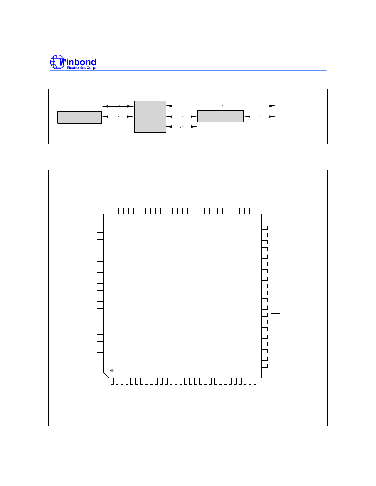
SYSTEM DIAGRAM .......................................................................................................................... 3
PIN CONFIGURATION...................................................................................................................... 3
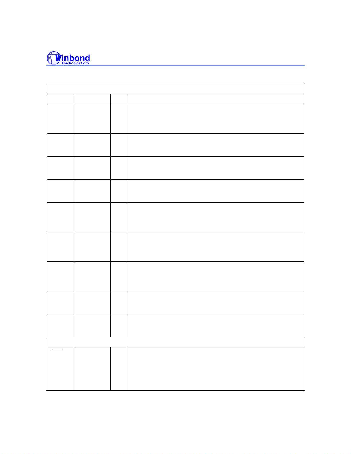
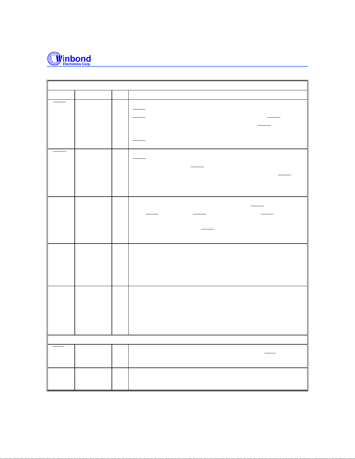
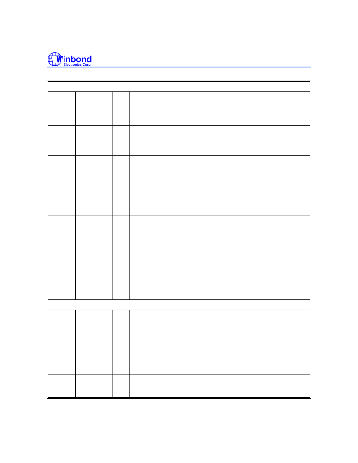
PIN DESCRIPTION ........................................................................................................................... 4
BLOCK DIAGRAM............................................................................................................................. 8
FUNCTIONAL DESCRIPTION........................................................................................................... 8
AUI Interface and Twisted Pair Line Transceiver..........................................................................................8
Link Test Function.........................................................................................................................................8
Automatic Polarity Reversal Function...........................................................................................................9
Port Partition/Reconnection Logic.................................................................................................................9
Port Status Direct Report Function...............................................................................................................9
Initial State After Reset...............................................................................................................................11
Management Logic and Management Interface .........................................................................................11
IMPR II Programmable Options..................................................................................................................15
The IMPR II Kernel Logic............................................................................................................................15
Inter-IMPR II Interface.................................................................................................................................16
ABSOLUTE MAXIMUM RATINGS................................................................................................... 17
DC CHARACTERISTICS................................................................................................................. 17
AC CHARACTERISTICS ................................................................................................................. 19
System Clock Timing..................................................................................................................................19
Reset Timing...............................................................................................................................................19
Management Bus Clock Timing..................................................................................................................20
Management Bus Carrier Sense Timing.....................................................................................................20
Inter-IMPR II Interface Input Timing............................................................................................................21
Inter-IMPR II Interface Output Timing .........................................................................................................22
Inter-IMPR II Interface Collision Timing.......................................................................................................23
Inter-IMPR II Interface to AUI/TP Port Timing.............................................................................................23
Output Driver Timing...................................................................................................................................24
Repetition Timing (part 1) ...........................................................................................................................24
Repetition Timing (part 2) ...........................................................................................................................25
Link Test Timing..........................................................................................................................................26
PACKAGE DIMENSIONS................................................................................................................ 28
Publication Release Date: November 1996
- 1 - Revision A1
Page 2

Preliminary W89C982AF
GENERAL DESCRIPTION
The Integrated Multiple Port Repeater II (IMPR II) implements the repeater functions specified by
section 9 of the IEEE 802.3 standard and twisted pair line transceiver functions conforming to the
10BASE-T standard. The IMPR II provides eight Twisted Pair (TP) Line Transceiver Ports and an
Attachment Unit Interface (AUI) port. Each Twisted Pair (TP) Line Transceiver Port can connect to an
Ethernet segment through a twisted pair line. The AUI port can connect to a thick Ethernet segment
by means of a 50-meter AUI cable. The IMPR II provides an AUI/TP port status direct report function,
which uses the ten port status pins and two select pins to indicate collisions, port link/activity,
partition, polarity, and network utilization. The inter-IMPR II interface includes signals for connecting
more than one IMPR II to increase the total number of hub ports. The manageable functions of the
repeater and twisted pair line transceiver in the IMPR II can be accessed through a serial interface.
FEATURES
• Functions conform to IEEE 802.3 section 9 specifications
• Single 5V power supply
• CMOS process for lower power dissipation
• Twisted-Pair (TP) line media interface compatible with 10 BASE-T specifications
• Differential interface compatible with AUI specifications
• Port status direct report function
• Asynchronous Inter-IMPR II interface for large hub applications
• Serial management interface allows for network management and makes port status information
accessible
• AUI and TP port carrier sense signals observable through a port activity monitor port
• Internal main state machine performs fragment extension, packet repetition, and collision handling
functions
• Internal jabber lockup protection state machine monitors the length of each input packet to prevent
transmission of excessively large packets
• Separate partition state machine for each TP port and AUI port can isolate ports when an excessive
number of collisions occur and reconnect them using certain algorithms
• On-chip PLL, Manchester encoder/decoder, and FIFO
ORDERING INFORMATION
TYPE NO. PACKAGE
W89C982AF 100-pin QFP
- 2 -
Page 3
SYSTEM DIAGRAM
Preliminary W89C982AF
Inter-IMPR II
Interface
Mngrmnt
Controller
Mngrmnt
Bus
PIN CONFIGURATION
R R
0
DD
81
82
83
84
85
86
87
88
89
90
91
92
93
94
95
96
97
98
99
100
1
2 3 4
RD6RD6+
RD5RD5+
RD4RD4+
AV
RD3RD3+
RD2RD2+
RD1RD1+
AVss
RD0RD0+
DIDI+
CICI+
IMPR II
D D D DVD D D D DD D D D DVD D
V
D
s s
D
s
+ - + - + - + -+ - + - + -
D
55556666777777
D
77777777778
Preequalizer
Port status direct report
VTT D D TT D D TT D D TT D D
s s
-
+
+
6666666666
1234567890123456789
W89C982AF
5 678 9 0
1 1 1 1 1 1 1 1 1
1 2 3 4
5 6 7 8 9 0
1
2 2 2 22 2 2 2 2 2 3
1 2
444 4
-
T
T
P
P
7
6
R
R
P
P
T
T
3
4
T
T
T
P
P
P
5
4
3
R
R
R
VD D
P
P
P
s
T
T
T
5 6 7 8 9
AUI
Twisted-pair
Media
T
P
2
R
V
D
P
D
T
5155555555
234567890
50
TP1RPT
49
TP0RPT
48
AUIRPT
47
XCOLRPT
46
ICRS
45
IDAT
44
IDCLK
43
DVss
42
IJAM
41
DV
DD
40
ICOL
39
IBEN
38
RST
37
TEST
36
DVss
35
X2
34
X1
33
DV
DD
32
PCRS
31
STR
0
P P D D D D D DV
L L
O O
TT
-
L L
+
0 0
V
D
D
+ -V
s
s
ssD D
0 0
+ -TT+ -
D D D D D D D D
V
D D
D
D
1 1
1 1
+ -
+ -
D D D DV MM MM M D
V
TT
D D
D
D
+ -TT+ -
D D
s
s2 2 2 2 3 3 3 3
+ -
10S SIC
OVs
L
s
K
Publication Release Date: November 1996
- 3 - Revision A1
Page 4
Preliminary W89C982AF
ICRS
PIN DESCRIPTION
NETWORK INTERFACE PINS
NAME NO. I/O DESCRIPTION
DO+
DO-
DI+
DI-
CI+
CI-
DT0+
to
DT7+
DT0to
DT7-
DD0+
to
DD7+
DD0to
DD7-
4
3
98, 97 I AUI Receive Input:
100, 99 I AUI Collision Input:
5, 11, 15,
20, 63, 68,
72, 78
6, 12, 16,
21, 62, 67,
71, 77
8, 13, 17,
23, 60, 66,
70, 75
9, 14, 18,
24, 59, 65,
69, 74
O AUI Transmit Output:
Differential line driver that sends differential signal to Medium
Attached Unit (MAU). These pins require a 270 ohm pull-down
resistor to GND.
Differential receiver that receives the AUI-compliant receive signal
from MAU.
Differential receiver that receives the AUI-compliant collision
signal from MAU.
O Data Positive:
Transmit data driver positive that transmits data on the twisted pair
line. The driver will source or sink 32 mA. The driver is low during idle.
O Data Negative:
Transmit data driver negative that transmits inverted data on the
twisted pair line. The driver will source or sink 32 mA. Driver is low
during idle.
O Delayed Data Positive:
Transmit data driver positive that transmits delayed inverted data
on the twisted pair line. The driver will source or sink 32 mA.
Driver is low during idle.
O Delayed Data Negative:
Transmit data driver negative that transmits delayed data on the
twisted pair line. The driver will source or sink 32 mA. Low during
idle.
RD0+
to
RD7+
RD0to
RD7-
96, 93, 91,
89, 86, 84,
82, 80
95, 92, 90,
88, 85, 83,
81, 79
46 O Inter-IMPR II Carrier Output:
I Twisted Pair Line Receive Positive:
Positive data from the twisted pair line are received by the internal
receiver through this pin.
Twisted Pair Line Receive Negative:
I
Negative data from the twisted pair line are received by the
internal receiver through this pin.
INTER-IMPR II INTERFACE PINS
The inter-IMPR II carrier (an active low on this pin) will be present
when the IMPR II is repeating packets. The IMPR IIs output this
signal to the interface of inter-IMPR II for retransmitting valid
packets or propogating network collision messages to other IMPR
IIs.
- 4 -
Page 5
Preliminary W89C982AF
IBEN
IBEN
IBEN
ICRS
ICRS
IBEN
ICOL
ICOL
ICRS
ICOL
ICRS
IBEN
ICRS
IBEN
IBEN
RST
RST
Continued
INTER-IMPR II INTERFACE PINS
NAME NO. I/O DESCRIPTION
39 I
40 I
IDCLK 44 IOInter-IMPR II Data Clock:
IDAT 45 I
IJAM 42 I
38 I IMPR II Reset:
MCLK 28 I Management Bus Clock:
Inter-IMPR II interface Enable:
is driven by HUB integrator. The integrator will drive the
low if there is only one IMPR II which outputs
inter-IMPR II interface. The IMPR II that asserts
allowed to transmit valid messages to the IMPR II integrator when
is low.
Inter-IMPR II Collision:
will be driven low when more than one IMPR II
simultaneously output
will not transmit any data to the IMPR II integrator when
low. On this situation the collision messages will still be sent to all
ports of the IMPR II.
IDCLK will drive a 10 MHz clock output when
and
IDCLK will be driven by the IDCLK signal of another IMPR II. If a
dumb hub is used, i.e., no
impedance. This pin is synchronous to IDAT data.
Inter-IMPR II Data:
The IMPR II sends/receives valid packets or inter-port collision
O
messages to/from other IMPR IIs through the IDAT pin in NRZ
Z
format. IDAT is in high-Z state during inter-IMPR II collisions or
when the network is idle. IDAT remains high when there is a
transmit collision in the IMPR II.
Inter-IMPR II IJAM:
IJAM is driven low when a valid packet is being sent. IJAM is
O
driven high when IDAT carries a collision message (i.e., always
Z
high or always low). IDAT = 0 indicates a multiport collision and
IDAT = 1 indicates a single port collision condition.
During inter-IMPR II collisions or when the network is idle, IJAM
should be in high-Z state.
MANAGEMENT BUS PINS
The IMPR II will be forced into its initial state when
low.
The management data are clocked by MCLK serially. The rising
edge of MCLK will latch the data into or out of the IMPR II.
is driven. If
to the IMPR II integrator. The IMPR II
is not asserted and
is present, this pin is in high
to the
will be
is
is asserted
is driven,
is driven
Publication Release Date: November 1996
- 5 - Revision A1
Page 6
Preliminary W89C982AF
Continued
MANAGEMENT BUS PINS
NAME NO. I/O DESCRIPTION
MSI 27 I Management Data in:
The management command is serially clocked into IMPR II by
MCLK.
MSO 29 O Management Data Out:
The network status or the internal management status of the IMPR
II is serially read out from MSO whenever the IMPR II receives a
status read command.
TEST 37 I IMPR II Test Mode:
This pin should be tied high during test mode and tied low during
normal operations.
PCRS 32 O Network Port Carrier Sense:
The carrier sense signals for the IMPR II's internal logic from the
AUI port and eight TP ports are serially sampled and output
through PCRS. The output bits are stream synchronized to X1
clock.
STR 31 O Network Port Carrier Sense Strobe:
The serial bit stream on PCRS can be latched by an external latch
using the STR signal. The STR goes high for two X1 clock cycles
after the nine carrier sense bits are output through PCRS.
X1 34 I System Clock Input:
An external 20 MHz system clock source is connected to this pin to
provide the operating clock. For crystal applications, a 20 MHz
crystal may be connected across pins X1 and X2.
X2 35 O Crystal Clock Feedback:
Pin X2 should be left floating when an external clock source is
used.
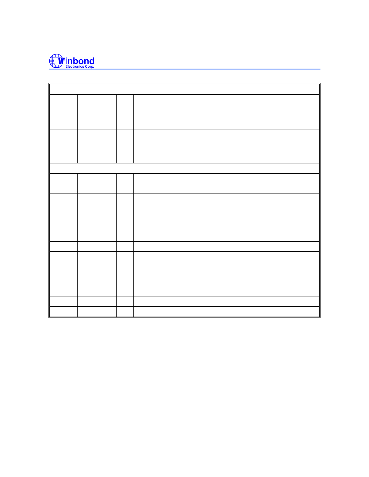
PORT STATUS DIRECT REPORT INTERFACE PINS
M1
M0
XCOLRPT
25
26
47 O Collision Status Direct Report Output: Whenever a collision event
I Port Status Direct Report Select Pins:
These two pins control the output status of the port status pins.
Four output states can be selected by M1, M0:
TP Link/Activity Partition Polarity error Utilization
AUI COL/Activity Partition Loopback error Utilization
M1 0 0 1 1
M0 0 1 0 1
occurs, this pin is active high. This pin drives a TTL data buffer,
which directly drives an LED.
- 6 -
Page 7
Preliminary W89C982AF
Continued
PORT STATUS DIRECT REPORT INTERFACE PINS
NAME NO. I/O DESCRIPTION
AUI RPT
TP0 RPT
TP7 RPT
VDD 10, 19, 52,
VSS 7, 22, 53,
AVDD 87 I TP Receive Power Supply: +5V DC power supply.
AVSS 94 I TP Receive Ground: Grounding pins.
PLL -
VDD
PLL VSS
48 O AUI Port Status Direct Report Output: This pin outputs the AUI port
status selected by M0/M1. This pin drives a TTL data buffer, which
directly drives an LED.
49−51,
54−58
64, 73
61, 76
1 I PLL Power Supply: +5V DC power supply.
2 I PLL Ground: Grounding pins.
O TP Port Status Direct Report Output: These pins output the TP
port status selected by M0/M1.
These pins drive a TTL data buffer, which directly drives an LED.
POWER GROUND PINS
I Power Supply for TP Transmit/Port Status Pins: +5V DC power
supply.
I Ground for TP Transmit/Port Status Pins.
This pin should be decoupled with a 22 µF capacitor and kept
separate from other power and ground planes.
This pin should be decoupled with a 22 µF capacitor and kept
separate from other power and ground planes.
DVDD 33, 41 I Digital Power Supply: +5V DC power supply.
DVSS 30, 36, 43 I Digital Ground: Grounding pins.
Publication Release Date: November 1996
- 7 - Revision A1
Page 8
BLOCK DIAGRAM
Preliminary W89C982AF
Twisted Pair Line
Transceiver 1
.
.
.
.
.
.
Twisted Pair Line
Transceiver 8
AUI
Interface
Management
Interface
Port status
direct report
Port Partition/
Reconnection
Logic
Timer and
Counters
Jabber lockup and
Fragment extension
Logic
Encoder and
Transmitter
Logic
Management
Logic
Rx MUX
Main state
Machine
and
Glue logic
Tx MUX
PLL
Decoder
FIFO
Control
Logic
Preamble/
JAM
Generator
MUX
FIFO
Inter-IMPR II
Interface
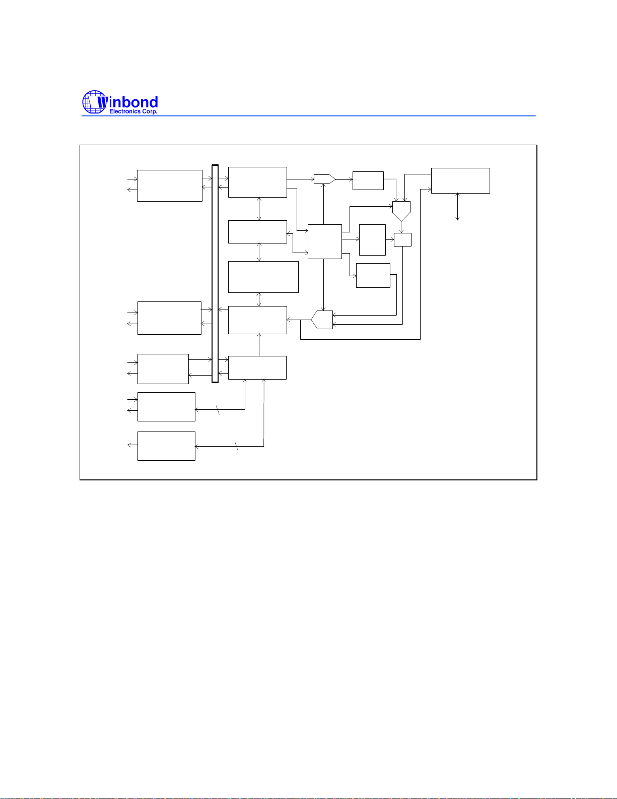
FUNCTIONAL DESCRIPTION
The Integrated Multiple Port Repeater II implements the functions stipulated in the IEEE repeater
specifications, the functions specified by 10BASE-T standards, and functions for network
management. It provides an Inter-IMPR II interface to allow implementation of a repeater set with
more network ports. The block functions of the IMPR II are described below.
AUI Interface and Twisted Pair Line Transceiver
The AUI provides an interface for an external Medium Attached Unit (MAU) connected to the IMPR II.
The IMPR II can be used to connect a 10BASE2 or 10BASE5 Ethernet to a 10BASE-T Ethernet via a
coaxial transceiver. The Twisted Pair Line Transceiver provides the interface used to connect IEEE
802.3 LAN stations (Data Terminal Equipment, or DTEs) into Ethernet networks constructed from
twisted pair media. The Twisted Pair Line Transceiver also contains a link test function and
autopolarity reversal function for wiring detection.
Link Test Function
The link test function of the TP port is used to check whether the TP port is linked to an active TP
port. The TP port will enter link fail state if it does not receive any packets or link test pulses for more
than 60 mS, until it receives either six consecutive link pulses or a packet. When the TP port is in link
- 8 -
Page 9

Preliminary W89C982AF
fail state, the IMPR II will not transmit any signal (packets or link pulses) on the TP port and the first
input packet will not be retransmitted. The IMPR II will transmit link test pulses to any TP port after
the transmitter of the TP port has been inactive for more than 16 mS after the TP port enters link
good state. The link test function of the TP port is user-programmable using the management
functions of the IMPR II. The TP port is forced into link good status if the link test function is disabled.
The link test function is enabled by default each time the IMPR II is reset.
Automatic Polarity Reversal Function
The automatic polarity reversal function checks the polarity of the input data packets or link pulses.
The polarity of the TP port will be set to negative when the polarity of the first input packet or the first
three consecutive link pulses following reset or following entry of the TP port into link fail state are
detected to be negative. Once the polarity of the TP port is set to negative, all consequent input
packets will be retransmitted with data that are inverted with respect to the input packet after the TP
port enters link good state. If the polarity of the TP port is not set to negative, all input packets will be
retransmitted without any modification of the data polarity. Once the polarity of the TP port is
determined, the polarity of this port will not be updated until the IMPR II is either reset or re-enters link
fail state, regardless of whether the automatic polarity reversal function is disabled or enabled. The
automatic polarity reversal function is user-programmable using the management functions of the
IMPR II and is enabled by default each time the IMPR II is reset. The default status of polarity is
"correct" when the IMPR II is in reset state.
Port Partition/Reconnection Logic
The port partition/reconnection logic implements the segment partitioning algorithm and the segment
reconnection algorithm. These algorithms are defined by IEEE specifications and are used to protect
the network from malfunctioning segments. There are nine partition/reconnection machines in an
IMPR II. Each port partition reconnection machine controls an individual network port.
A network port will be partitioned by the IMPR II when either of the following conditions is detected:
(1) A collision condition exists continuously for a period of up to 1024 bit times.
(2) Thirty-two consecutive collisions occur.
A collision condition is defined as more than two network ports attempting to transmit simultaneously
or as a receive collision from the AUI.
The IMPR II can reconnect a partitioned network port using algorithms selected by programming the
management logic. The following are the two reconnection algorithms:
(1) Standard reconnection algorithm:
A partitioned network port will be reconnected if a data packet longer than 512 bit times is
retransmitted to or received from that port without collision.
(2) Alternative reconnection algorithm:
A partitioned network port will be reconnected if a data packet longer than 512 bit times is
retransmitted to that port without collision.
The reconnection algorithms for all the TP ports and the AUI port are programmed individually;
however, all the TP ports use the same algorithm. The standard algorithm is selected by default each
time the IMPR II is reset.
Port Status Direct Report Function
Publication Release Date: November 1996
- 9 - Revision A1
Page 10
Preliminary W89C982AF
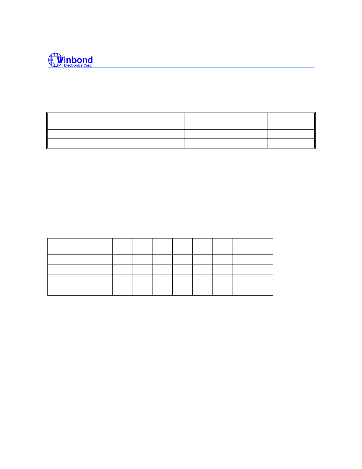
The IMPR II provides one pin (XCOLRPT) for collision status report, two pins (M0/M1) for port status
report mode selection, and nine pins for port status report (AUIRPT, TP0-7RPT). XCOLRPT is active
when a collision occurs. Each of the nine port status report pins can directly report four aspects of the
port status. Which aspect of the network status is reported by these pins is determined by the two
mode selection pins, M1 and M0, as shown in the table below.
UTILIZATION
UTILIZATION
M1
M0
TP LINK/ACTIVITY
AUI COL/ACTIVITY
0 0 1 1
0 1 0 1
PARTITION TP POLARITY
AUI LOOPBACK ERROR
When M0 and M1 are set to "0," the pins report TP link/activity and AUI COL/activity. In this mode, a
low output on AUIRPT and TP0-7RPT means all the TP ports are in the link fail state, a high means
all the TP ports are in link good state, and the AUI is in collision state, and a 10 Hz signal means
incoming packets are being received by the AUI/TP ports. (Note that the 10 Hz signal is still reported
if the ports are partitioned or disabled.) If M0 is set to "1" and M1 to "0," the port partition status will be
reported. In this mode, a "0" output means that all the ports are connected correctly, and a "1" means
that the AUI/TP ports are in a partition state. When M0 is set to "0" and M1 to "1," AUI loopback
errors and TP polarity status will be reported. In this mode, a "0" output means that the AUI loopback
and TP polarity are correct, and a "1" means that an AUI loopback error has been detected and the
TP port polarity is reversed. If M0 and M1 are both set to "1," the network utilization will be reported.
In this mode, each LED stands for 10% of utilization. The percentage of network utilization is shown
the following table.
% OF
UTILIZATION
AUI
LED
TP0
LED
TP1
LED
TP2
LED
TP3
LED
TP4
LED
TP5
LED
TP6
LED
TP7
LED
10% v
30% v v v
50% v v v v v
90% v v v v v v v v v
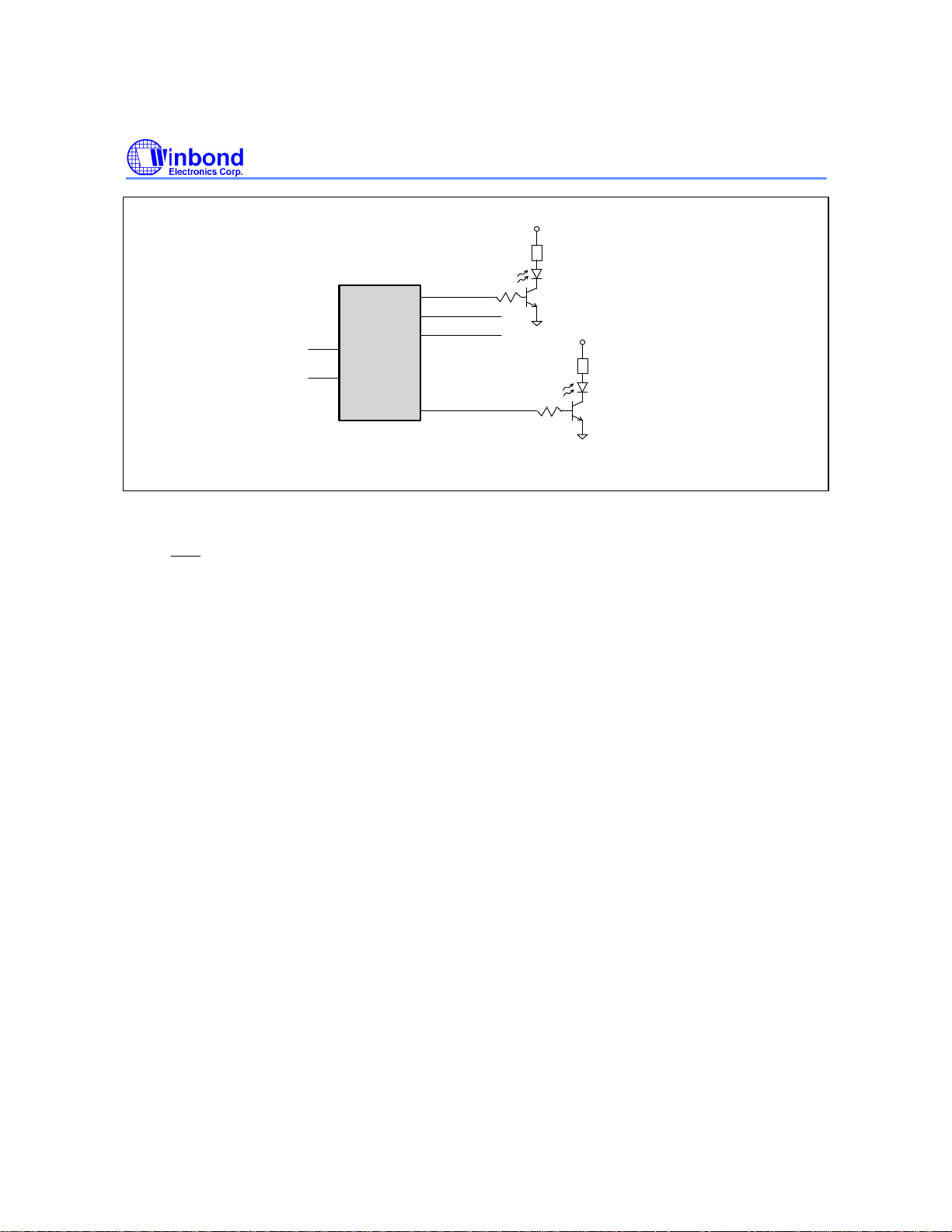
Using pins M1 and M0 and external transistors, the IMPR II can drive LEDs to indicate the status of
the AUI/TP ports sequentially; the application circuit for the LEDs is shown below. If a simple decoder
is connected to pins M1 and M0 and a switch circuit is connected to TP0RPT to TP7RPT, the TP port
link/activity, partition, polarity, and network utilization can be displayed simultaneously.
- 10 -
Page 11
M1
RST
M0
Initial State After Reset
W89C982AF
* Set M1, M0 to select port status output.
XCOLRPT
AUIRPT
TP0RPT
.
.
.
.
.
TP7RPT
Preliminary W89C982AF
R
R = 330
Collision LED
.
.
.
R
.
R = 330
TP7 status LED
When
is driven low, the IMPR II is reset. The minimum time the reset signal must be held low to
trigger a reset is 100 µS. During reset, the IMPR II places all outputs in the inactive state (except for
the auto polarity reversal function). Active low outputs stay high, active high outputs stay low, link test
is enabled, and the TP link is in a fail state. The AUI/TP auto partition/reconnection uses the standard
algorithm, AUI/TP transmitters are idle, AUI/TP receivers are enabled, IDAT and IJAM are in highimpedance state, STR is low, and the auto polarity reversal function is enabled.
Management Logic and Management Interface
The major functions of the management logic are enabling/disabling networks, partitioning/reconnecting network ports, enabling/disabling the link test and autopolarity reversal functions of the
twisted pair line transceiver, and accessing the link status and polarity status of the twisted pair line
transceiver. The management interface is a signal bus that contains input/output signals to/from the
management logic and the internal carrier sense signals for the nine network ports of the IMPR II.
The management logic can accept and execute management commands when the IMPR II is in
normal mode, i.e., the TEST pin of the IMPR II is tied low. All management commands are byteoriented and are clocked into the IMPR II serially by an external clock. Some of the commands
require an output from the IMPR II in response and some do not. At least 20 clocks are required to
send a command that requires an output response from the IMPR II; 14 clocks are needed to send a
command that requires no response. The serial command data stream and any associated output
response data stream are structured in a manner compatible with the RS232 serial data format, i.e.,
one start bit followed by eight data bits, with the LSB sent first and the MSB last.
Publication Release Date: November 1996
- 11 - Revision A1
Page 12
Preliminary W89C982AF
The following table summarizes the management commands. The LSBs of both the MSI data and the
MSO data are shown on the right and the MSBs are shown on the left. Each command is described in
more detail below.
MSI INPUT DATA MSO READ DATA FUNCTIONS
11010000 P7 . . . P0 Read link test status of TP ports
11100000 P7 . . . P0 Read polarity status of TP ports
10000000 P7 . . . P0 Read partition status of TP ports
10001111 P7 . . . P0 Read bit rate error status of TP ports
11110000 M0000000 Read MJLP status
10001111 PBSL0000 Read AUI port status (B, S, L cleared)
10001011 PBSL0000 Read AUI port status (S, L cleared)
10001101 PBSL0000 Read AUI port status (B cleared)
10001001 PBSL0000 Read AUI port status (None cleared)
00111111 None Enable AUI port
00101111 None Disable AUI port
00110bbb None Enable TP ports
00100bbb None Disable TP ports
01010bbb None Enable TP port link test function
01000bbb None Disable TP port link test function
01110bbb None Enable TP ports auto polarity reversal function
01100bbb None Disable TP ports auto polarity reversal function
00011111 None Set AUI port alternate reconnection algorithm
00010000 None Set TP port alternate reconnection algorithm
00001CSA None Set IMPR II programmable option
Read Link Test Status of TP Ports
The link test status of all eight TP ports can be read using this command. Bits 0 through 7 correspond
to the link test status of TP ports 0 through 7. A "1" on the MSO bit indicates "Link Good" status and a
"0" indicates "Link Fail" status.
Read Polarity Status of TP Ports
The polarity status of all eight TP ports can be read using this command. Bits 0 through 7 correspond
to the polarity status of TP ports 0 through 7. A "1" on the MSO bit indicates reversed polarity and a
"0" indicates positive polarity.
Read Partition Status of TP Ports
The partition status of all eight TP ports can be read using this command. Bits 0
through 7 correspond to the polarity status of TP ports 0 through 7. A "1" on the MSO
bit indicates a connected status and a "0" indicates a partitioned status.
- 12 -
Page 13
Preliminary W89C982AF
Read Bit Rate Error Status of TP Ports
The bit rate error status of the TP ports can be read using this command. Bits 0 through 7 correspond
to the polarity status of TP ports 0 through 7. A "1" on the MSO bit indicates that a bit rate error has
occurred and a "0" indicates no bit rate error has occurred.
Read MJLP Status
The MAU jabber lock-up protection status can be accessed using this command. A "1" on the MSB
indicates the transmit function of the IMPR II has been inhibited. The status can also be cleared using
this command.
Read AUI Port Status
The AUI port status, including partition, bit rate error, SQE test, and loopback error, can be accessed
using different variations of this command. Four different specific commands can be used, as shown
in the following table.
MSI DATA MSO DATA CLEAR BITS
10001111 PBSL0000 B, S, L read cleared. P not cleared.
10001011 PBSL0000 S, L read cleared. P, B not cleared.
10001101 PBSL0000 B read cleared. P, S, L not cleared.
10001001 PBSL0000 P, B, S, L not cleared.
Enable AUI Port
When disabled, the AUI port can be re-enabled using this command. The AUI port will then carry out
normal transmitting and receiving operations. To reconnect a partitioned AUI port, the port must first
be disabled and then re-enabled using this command.
Disable AUI Port
This command is used to disable the AUI port. When the AUI port is disabled, all inputs (the carrier
sense and the SQE) to the AUI port will be ignored by the IMPR II and the IMPR II will not transmit
any signal on the AUI port. In addition, the partition machine for the AUI port will be forced into idle
status.
Enable TP Ports
This command is used to enable a disabled TP port, allowing it to perform normal transmitting and
receiving operations. To reconnect a partitioned TP port or force a TP port into link fail state, the port
must first be disabled and then re-enabled using this command.
Disable TP Ports
Each TP port can be disabled individually. Bits 0, 1, and 2 are used to indicate the TP port that is to
be disabled, as follows:
Publication Release Date: November 1996
- 13 - Revision A1
Page 14
Preliminary W89C982AF
B2 B1 B0 TP PORT DISABLED
0 0 0 TP0
0 0 1 TP1
0 1 0 TP2
0 1 1 TP3
1 0 0 TP4
1 0 1 TP5
1 1 0 TP6
1 1 1 TP7
When a TP port is disabled, all inputs (the carrier sense) to that port will be ignored by the IMPR II
and the IMPR II will not transmit any signal on the port. The partition machine for the port will be
forced into the idle state and the link test will indicate that the port is in the "Link Fail" state.
Enable TP Port Link Test Function
This command is used to re-enable a link-test disabled TP port. Using this command on a TP port
that is already enabled will have no effect on the port.
Disable TP Port Link Test Function
The TP port link test function can be enabled or disabled port-by-port. Bits 0, 1, and 2 are used to
select which TP port is to be disabled in the manner described under the "Disable TP ports" command
above. Once the link test function is disabled, the TP port will not enter the link fail state.
Enable TP Port Auto Polarity Reversal Function
The auto polarity reversal function of the TP ports can be enabled or disabled port-by-port. Bits 0, 1,
and 2 are used to indicate which TP port is to be enabled, in the manner described under the "Disable
TP ports" command above. When the auto polarity reversal function is enabled, the TP port will
check the polarity of input packets once it enters the link fail state. This function is enabled by default
each time the IMPR II is reset.
Disable TP Port Auto Polarity Reversal Function
This command is used to disable the auto polarity reversal function of a TP port so that the port will
no longer check the polarity of input packets. If an input packet with reversed data is received, the
IMPR II will not correct the polarity and retransmit the packet to all the network ports. In this case,
failure to reverse the polarity may cause a network error.
Set AUI Port Alternative Reconnection Algorithm
The partition/reconnection scheme can be programmed for the alternative (transmit only)
reconnection algorithm using this command. To return the partition/reconnection logic of the AUI port
back to the standard reconnection (transmit or receive) algorithm, the IMPR II must be reset.
Set TP Port Alternative Reconnection Algorithm
The partition/reconnection scheme can be programmed for the alternative (transmit only)
reconnection algorithm using this command. To return the partition/reconnection logic of a TP port
back to the standard reconnection (transmit or receive) algorithm, the IMPR II must be reset.
- 14 -
Page 15

Preliminary W89C982AF
The other main function of the management logic is the port activity monitoring function. The internal
carrier sense signal of all network ports is sampled out serially. The accuracy of the carrier sense
signals is 10 bit times. The first bit samples the internal carrier sense signal of the AUI port, the
second bit samples TP0, the third bit samples TP1, and so forth. The tenth bit time is idle, and a
strobe signal will be active during the tenth bit time. With the help of the strobe signal, the serial
sampled carrier sense signal can be latched to a serial-to-parallel shifter.
IMPR II Programmable Options
Three IMPR II programmable options can set by this command via the appropriate bit in MSI data.
The three programmable options are CI reporting, AUI SQE test mask, and alternative port activity
monitor function, which correspond to bits C, S, and A, respectively.
CI Reporting
Setting bit C = 1 will alter the function of the STR pin. STR will become an input pin for repeater
management devices and PCRS will insert the CI bit immediately before the AUI bit.
AUI SQE Test Mask
Setting S = 1 will disable the AUI SQE test when the SQE signal is within the SQE test window and
no jam pattern will be asserted after transmitted packets. The SQE test window is from 6 bit times to
34 bit times. When the SQE signal is larger than the SQE test window, a collision condition has
occurred.
Alternative Port Activity Monitor
Setting A = 1 will enable the alternative PAM function, so that repeater management devices can
monitor the status of each port using the unmodified PCRS signal.
The IMPR II Kernel Logic
The kernel logic of the IMPR II includes a main state machine and glue logic, timers and counters,
jabber lockup and fragment extension logic, a PLL decoder, encoder and transmitter, a 64-bit FIFO
with FIFO control logic, and a preamble/jam generator. These blocks perform most of the operations
needed to fulfill the requirements of the IEEE repeater specification. When a packet is received by a
connected port, it is sent via the receive multiplexer to the PLL decoder. Data and collision status are
sent to the main state machine via the port partition/reconnection logic. This enables the main state
machine to determine the source of data to be repeated and the type of data to be transmitted. The
transmit data may be either the received packet's data field or a preamble/jam pattern consisting of a
1010... bit pattern.
Associated with the main state machine are a series of timers and counters which ensure that various
IEEE specification times (referred to as the TW1 to TW6 times) are fulfilled. The PLL decoder
decodes the received data from Manchester code format into NRZ format and recovers the jitter
accumulated over the receiving segment.
The preamble/jam generator and the FIFO compensate for the preamble bit loss caused by
receptions by the twisted pair line transceiver. The FIFO is used to store the bits of the data field
temporarily while the preamble/jam generator is sending the preamble of the transmitting packet. A
1010... jam pattern is generated under network collision conditions.
The jabber lockup and fragment extension logic monitors the retransmitted packet. A jam pattern will
be appended to short packets (less than 96 bits in length) to extend them to a full 96 bits. The jabber
Publication Release Date: November 1996
- 15 - Revision A1
Page 16
Preliminary W89C982AF
ICRS
IBEN
ICOL
ICRS
IBEN
ICOL
ICRS
IBEN
ICOL
ICRS
IBEN
ICOL
ICRS
IBEN
ICOL
IBEN
ICOL
lockup and fragment extension logic will inhibit the encoder/transmitter logic when the retransmitted
packet is more than 65536 bits in length.
Packet repetition and network collision handling are performed by the main state machine according
to IEEE specifications. Soon after the network port receiving data packet has been identified, the
main state machine enables the preamble/jam generator to generate a preamble pattern onto the
encoder/transmitter. While the preamble is being transmitted, the received data are still being
monitored. The main state machine will enable the FIFO control logic to read the valid data into the
FIFO when the start of frame delimiter "SFD" is detected. A 1011 bit pattern is filled into the FIFO
before the SFD is detected. Removal of the FIFO data begins after a 60-bit preamble pattern has
been sent.
Inter-IMPR II Interface
The inter-IMPR II interface are designed for large hub applications. The inter-IMPR II interface allows
a minimum of four IMPR IIs to be integrated together to implement a hub with 32 twisted pair line
ports and four AUI ports. An external integrator is needed to handle the IMPR IIs. The data transfers
on the inter-IMPR II interface are in NRZ format and certain signals are used to indicate the network
status. Signals included on the inter-IMPR II interface allow the IMPR IIs to cooperate with each other
in an appropriate manner. Those signals include IDAT, IDCLK, IJAM,
,
receive data when the IMPR II asserts
deasserted
IMPR II integrator. When the IMPR II has not asserted
and deasserted
,
, IJAM, are the control signals. The IDAT and IDCLK are used to transmit or
and the external integrator asserted
to each IMPR II. The IDAT and IDCLK transmit data and a 10 MHz clock to the
and the integrator has asserted
to each IMPR II , the IMPR II receives the data and a 10 MHz clock from IDAT
and IDCLK. When IJAM is asserted, it indicates that a single port collision (IDAT = 1) or a multiport
collision (IDAT = 0) is occurring.
,
, and
. The
and
IMPR II Integrator
ICRSBa
X1a X1b X1c
IDATa,
IDCLKa,
IJAMa
982Aa
IBENBa,
ICOLBa
ICRSBb
IDATb,
IDCLKb,
IJAMb
982Ab
IBENBb,
ICOLBb
ICRSBc
IDATc,
IDCLKc,
IJAMc
982Ac
IBENBc,
ICOLBc
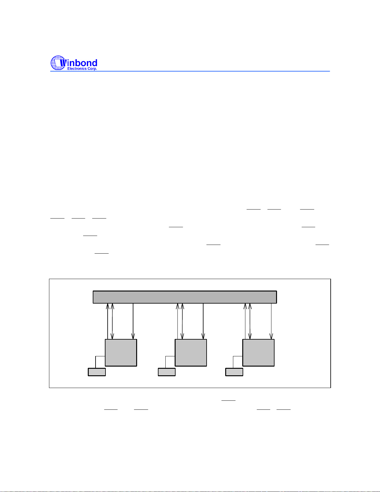
The figure above depicts an inter-IMPR II application circuit. The circuit requires an external inter
IMPR II integrator. The external integrator integrated the
generates signals,
and
, to the IMPR II. Each IMPR II checks
signal from each IMPR II and
,
to handle the
IDAT, IDCLK, IJAM signal direction.
Note that the inter-IMPR II uses different clocks source (X1a, X1b, X1c, etc.) to construct a large scale repeater application.
- 16 -
Page 17
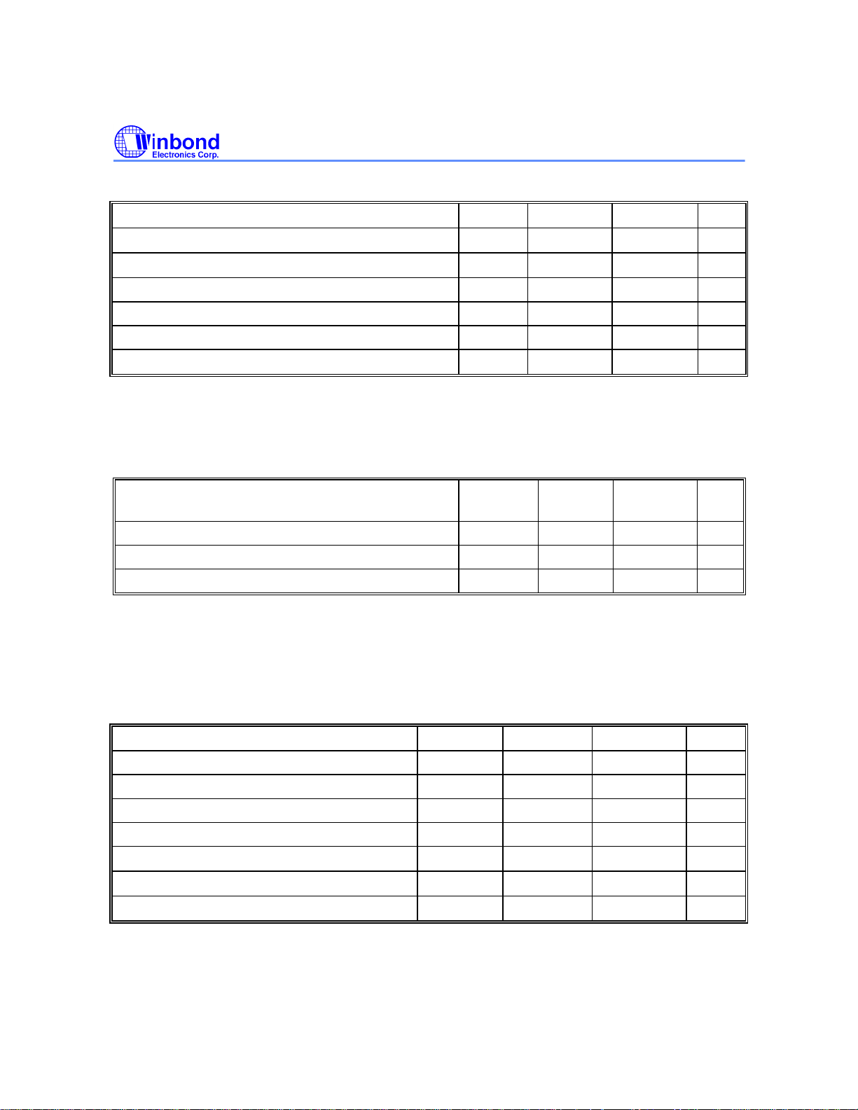
ABSOLUTE MAXIMUM RATINGS
PARAMETER SYM. MINIMUM MAXIMUM UNIT
Preliminary W89C982AF
Operating Temperature TA 0 70
Storage Temperature TS -55 150
°C
°C
Supply Voltage VDD -0.5 7.0 V
Input Voltage VIN VSS -0.5 VDD +0.5 V
Output Voltage VOUT VSS -0.5 VDD +0.5 V
Lead Temperature (soldering 10 seconds maximum) Tl -55 250
Note: Exposure to conditions beyond those listed under Absolute Maximum Ratings may adversely affect the life and reliability of the
device.
°C
Power Supply
(VDD = 4.75 to 5.25V, VSS = 0V, TA = 0° C to 70° C)
PARAMETER SYMBOL TYPICALMAXIMUMUNI
T
Power Supply Current (idle) IDDI - 100 mA
Power Supply Current (transmitting with no TP load) IDDT - 300 mA
Power Supply Current (transmitting with TP load) IDDL - Note mA
Note: For a TP typical load, each TP port will require an additional IDD current (maximum 32 mA). Less than 20% of the power will
be dissipated by the IMPR II, the remaining power is dissipated by the external TP load.
DC CHARACTERISTICS
(VDD = 4.75V to 5.25V, VSS = 0V, TA = 0° C to 70° C)
Digital
PARAMETER SYMBOL MINIMUM MAXIMUM UNIT
Low Input Voltage VIL VSS -0.5 0.8 V
High Input Voltage VIH 3.85 VDD +0.5 V
High Output Voltage (VDD = 4.5V) VOL 0.4 V
High Output Voltage (VDD = 4.5V) VOH 2.4 V
Input Leakage Current (Note 1) IIL1 10
Input Current (Note 2) IIL2 500
Output Leakage Current (VDD = 5.5V) IOL 10
Notes:
1. All of the input pins except those stated in Note 2.
2. TEST, IBENB, ICOLB, MSI, X1, M0, M1, these pins had been pull low or pull high.
Publication Release Date: November 1996
- 17 - Revision A1
µA
µA
µA
Page 18
Preliminary W89C982AF
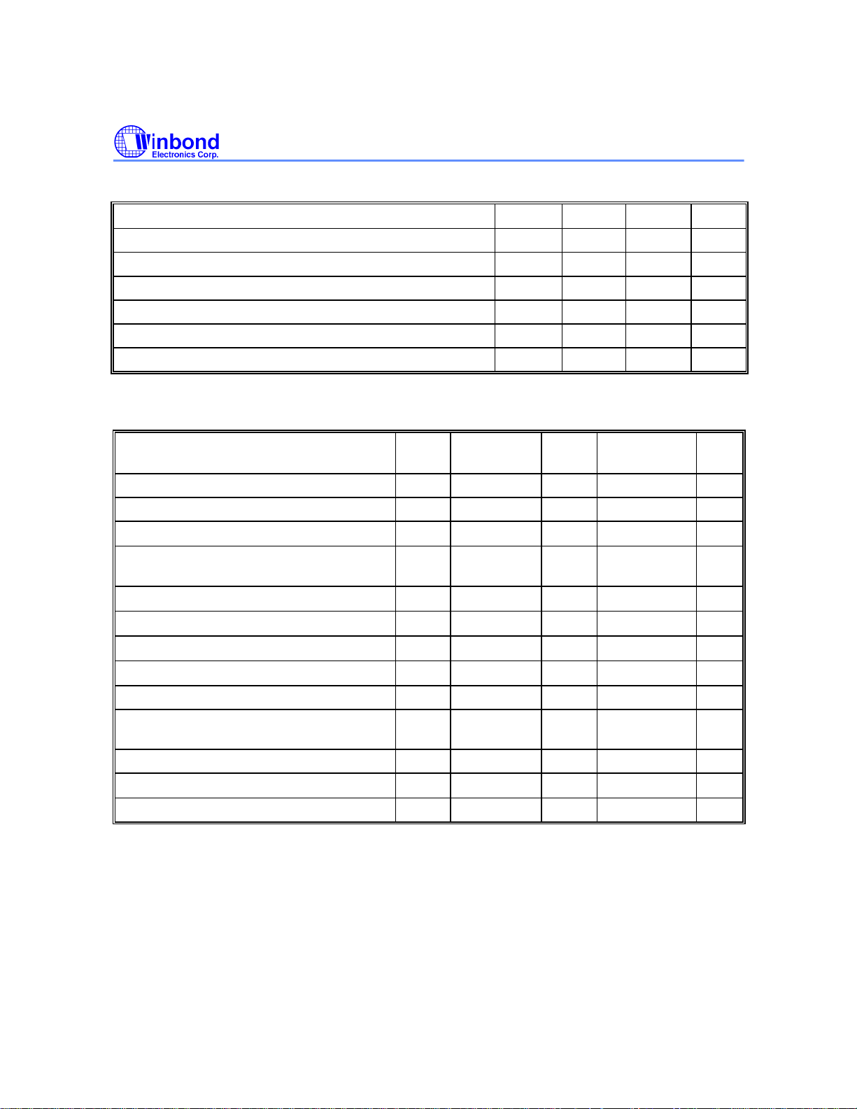
AUI
PARAMETER SYM. MIN. MAX. UNIT
Input Current at CI+/-, DI+/- pairs IIA 2 mA
Differential Output Voltage (DO+/-) VDD +/-550 +/-1200 mV
Differential Output Voltage Imbalance (DO+/-) VOB 40 mV
Undershoot Voltage (DO+/-) VU 100 mV
Differential Squelch Threshold (CI+/-, DI+/-) VDS -175 -300 mV
Differential Input Common Mode Voltage (DI+/-, CI+/-) VCM 1 4.0 V
Twisted Pair
PARAMETER SYM. MIN. TYP. MAX. UNI
Power Supply Voltage VDD 4.5 5.0 5.5 V
Input Voltage VIN -0.3 VDD +0.3
T
RD+/- Differential Input Resistance RTI 10
RD+/- Differential Input Voltage (VDD =
5V)
RD+/- Squelched Threshold VTPS
RD+/- low Squelched Threshold VTPU
RD+/- Input Switching Threshold VRDT
DT+, DT-, DD+, DD- Imbalance Voltage VTDU
DT+, DT-, DD+, DD- High Output Voltage VTOH
DT+, DT-, DD+, DD- Low Output Voltage
(I = 32 mA)
DT+, DT-, DD+, DD- Output Current ITO 32 mA
DT+, DT-, DD+, DD- Output Resistance RTO 5 8
Pad Capacitance CLD 7 10 pF
VTIV
VTOL VSS TP
±0.3 ±3.1
±300 ±400 ±585
±150 ±220 ±300
±5 ±10 ±20
VDD TP -0.44
±40
VDD TP V
VDD TP +0.44
KΩ
V
mV
mV
mV
mV
V
Ω
- 18 -
Page 19
Preliminary W89C982AF
43521
X1
RST
RST
X1
32RST
1
AC CHARACTERISTICS
(VDD = 4.75V to 5.25V, VSS = 0V, TA = 0° C to 70° C)
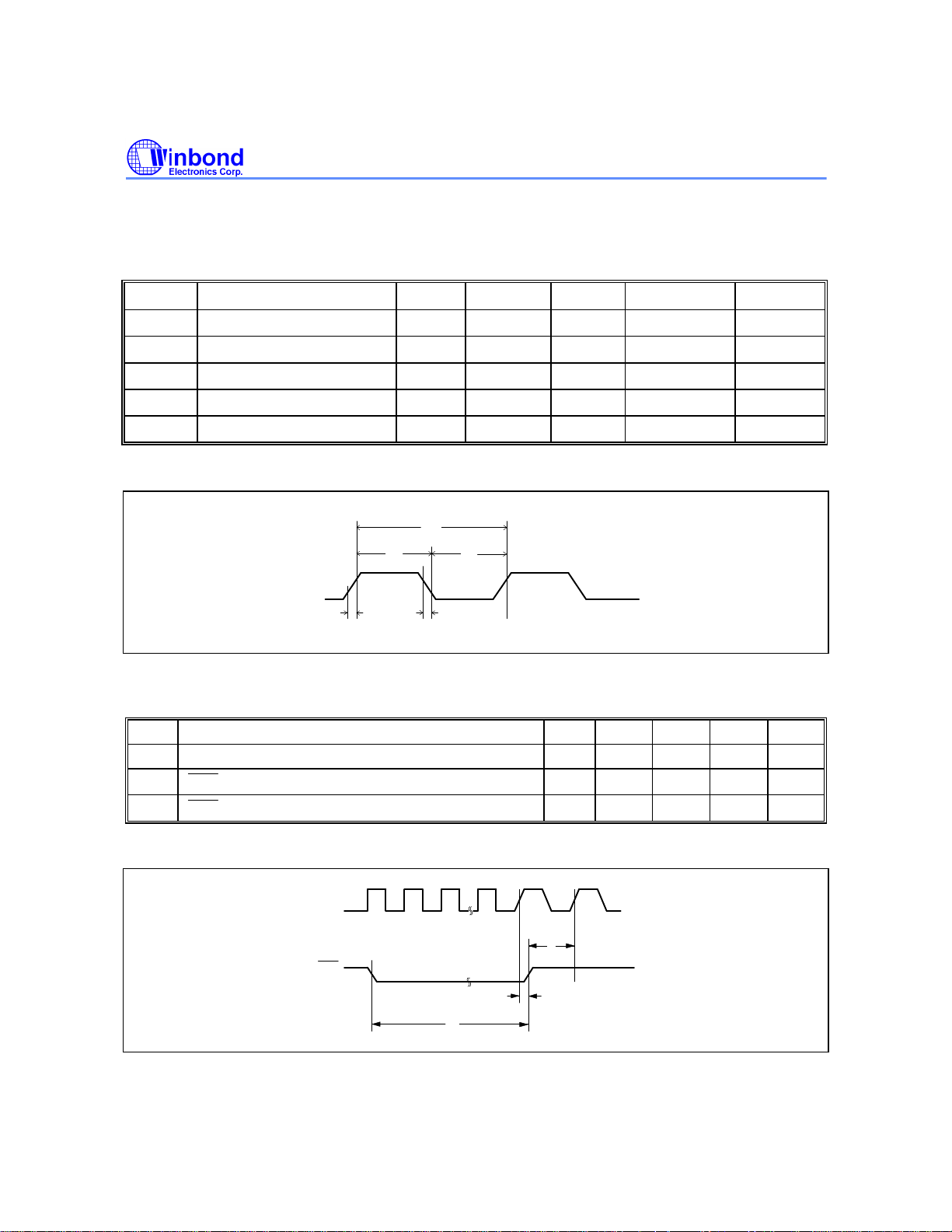
System Clock Timing
NO. DESCRIPTION FIG. MIN. TYP. MAX. UNIT
1 X1 clock rising time 1 10 nS
2 X1 clock falling time 1 10 nS
3 X1 clock period 1 49.995 50.005 nS
4 X1 clock high 1 22.5 27.5 nS
5 X1 clock low 1 22.5 27.5 nS
System Clock Timing Diagram
Figure 1
Reset Timing
NO. DESCRIPTION FIG. MIN. TYP. MAX. UNIT
1 Reset pulse width 2 100
2
3
Low hold time with respect to X1 clock
High setup time with X1 clock rising time
2 5 nS
2 20 nS
Reset Timing Diagram
Figure 2
µS
Publication Release Date: November 1996
- 19 - Revision A1
Page 20
Preliminary W89C982AF
321
MCLK4567
MSI
MSO
8
X1
PCRS
STR123AUI
TPO
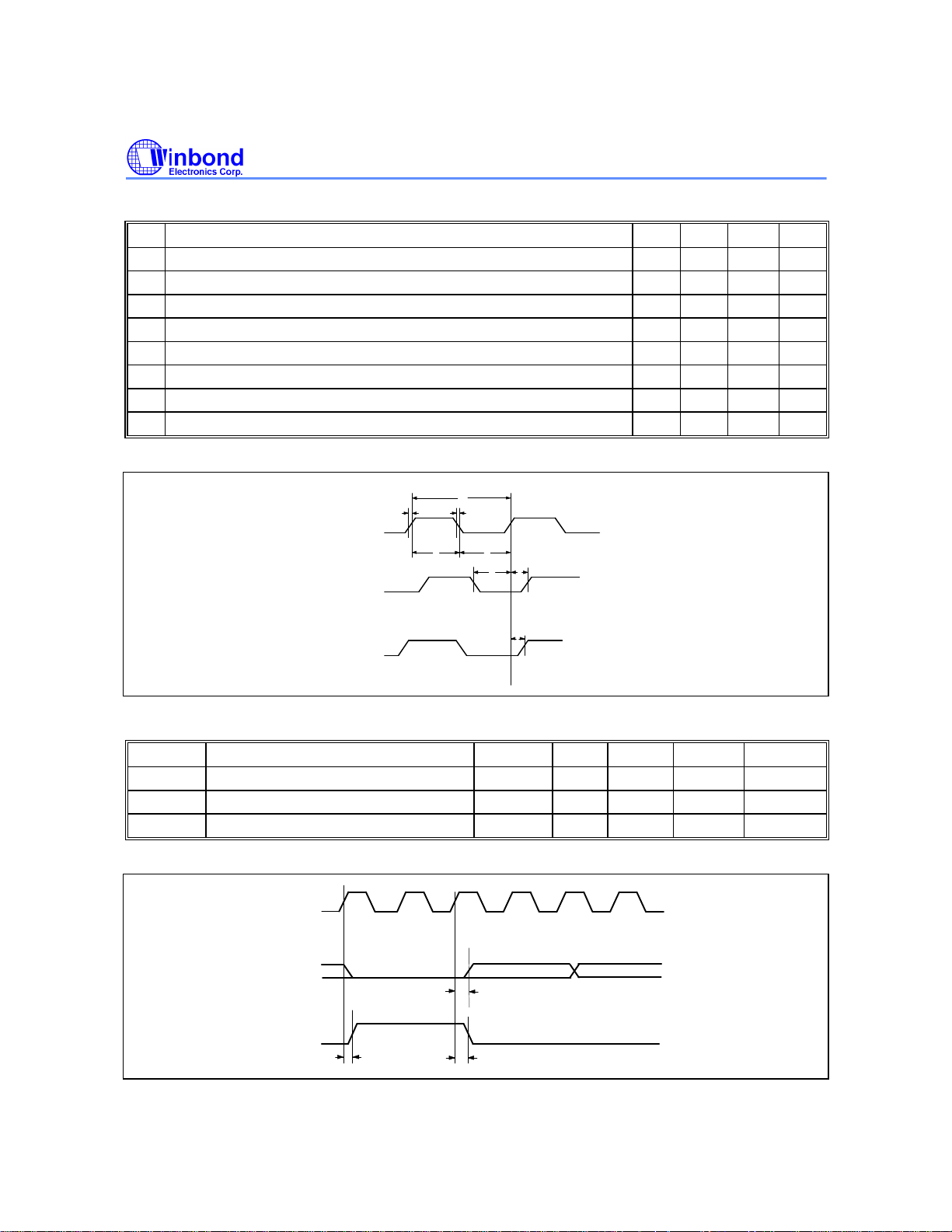
Management Bus Clock Timing
NO. DESCRIPTION FIG. MIN. MAX. UNIT
1 MCLK Clock Rising Time 3 10 nS
2 MCLK Clock Falling Time 3 10 nS
3 MCLK Clock Period 3 100 nS
4 MCLK Clock High 3 30 nS
5 MCLK Clock Low 3 30 nS
6 MSI Input Data Setup Time with Respect to MCLK Rising Edge 3 10 nS
7 MSI Input Data Hold Time with Respect to MCLK Rising Edge 3 10 nS
8 MSO Output Data Delay with Respect to MCLK Rising Edge 3 40 nS
Management Bus Clock Timing Diagram
Figure 3
Management Bus Carrier Sense Timing
NO. DESCRIPTION FIG. MIN. TYP. MAX. UNIT
1 X1 Rising Edge to STR High 4 40 nS
2 X1 Rising Edge to STR Low 4 40 nS
3 X1 Rising Edge to Valid PCRS 4 40 nS
Management Bus Carrier Sense Timing Diagram
Figure 4
- 20 -
Page 21
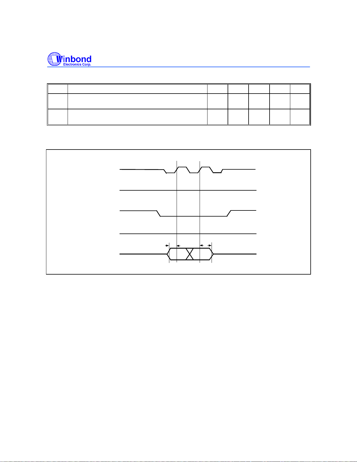
Preliminary W89C982AF
Inter-IMPR II Interface Input Timing
NO. DESCRIPTION FIG. MIN. TYP. MAX. UNIT
1 Receive-in IDAT/IJAM setup time to receive-in
IDCLK rising
2 Receive-in IDAT/IJAM hold time from receive-in
IDCLK rising
Inter-IMPR II Interface Input Timing Diagram
5 20 nS
5 20 nS
IDCLK
ICRSB
IBENB
ICOLB
IDAT
IJAM
High_Z
1
Figure 5
High_Z
2
Publication Release Date: November 1996
- 21 - Revision A1
Page 22
Preliminary W89C982AF
ICRS
IBEN
ICRS
IBEN
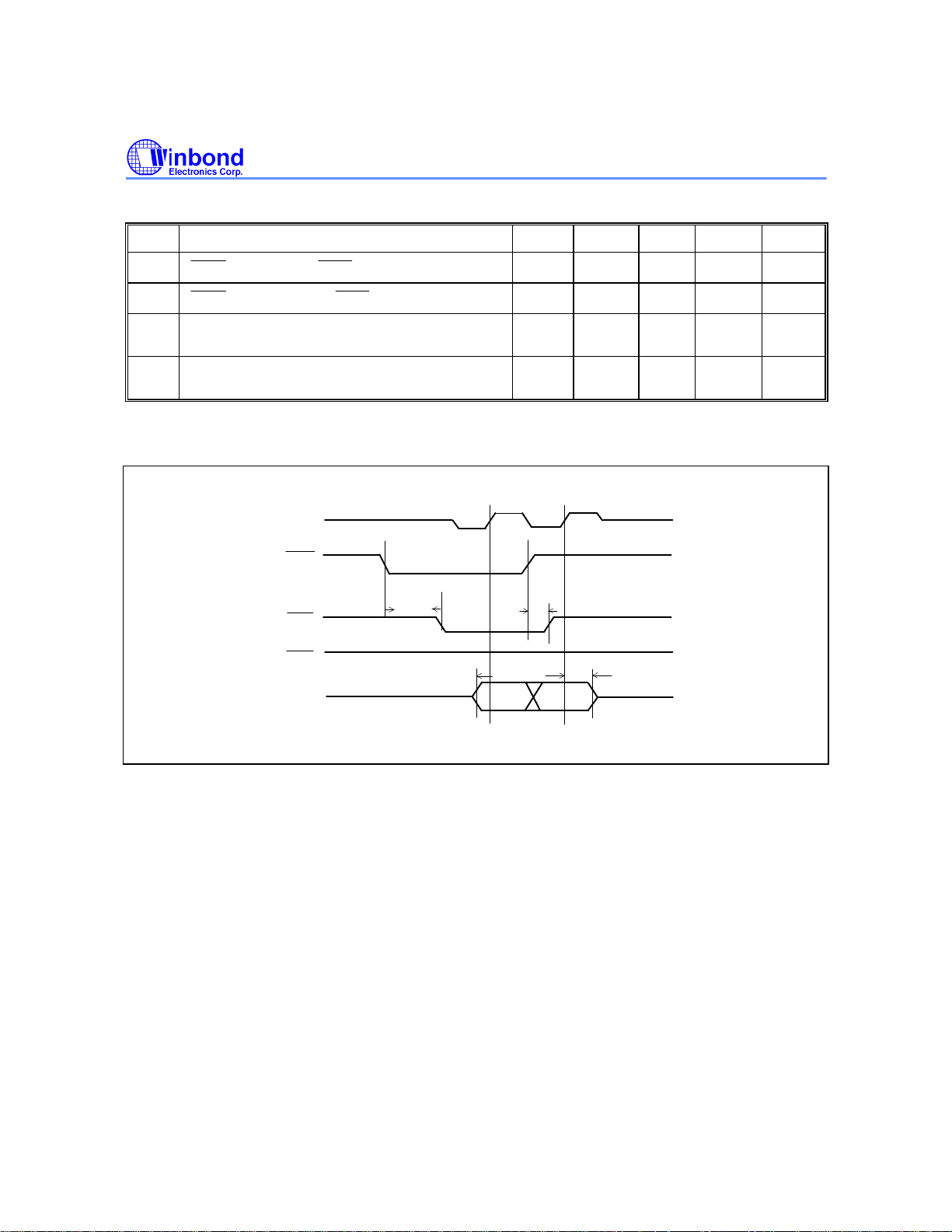
Inter-IMPR II Interface Output Timing
NO. DESCRIPTION FIG. MIN. TYP. MAX. UNIT
1
2
3
asserted to
deasserted to
asserted
deasserted
Transmit-out IDAT/IJAM setup time to
transmit-out IDCLK rising
Transmit-out IDAT/IJAM hold time from
4
transmit-out IDCLK rising
Inter-IMPR II Interface Output Timing Diagram
IDCLK
ICRS
IBEN
ICOL
IDAT
IJAM
High_Z High_Z
1
3
6 35 nS
6 35 nS
6 30 nS
6 30 nS
2
4
Figure 6
- 22 -
Page 23
Preliminary W89C982AF
ICRS
ICOL
ICRS
ICOL
2
1
DI+/-
DT-
IDAT
Valid Data
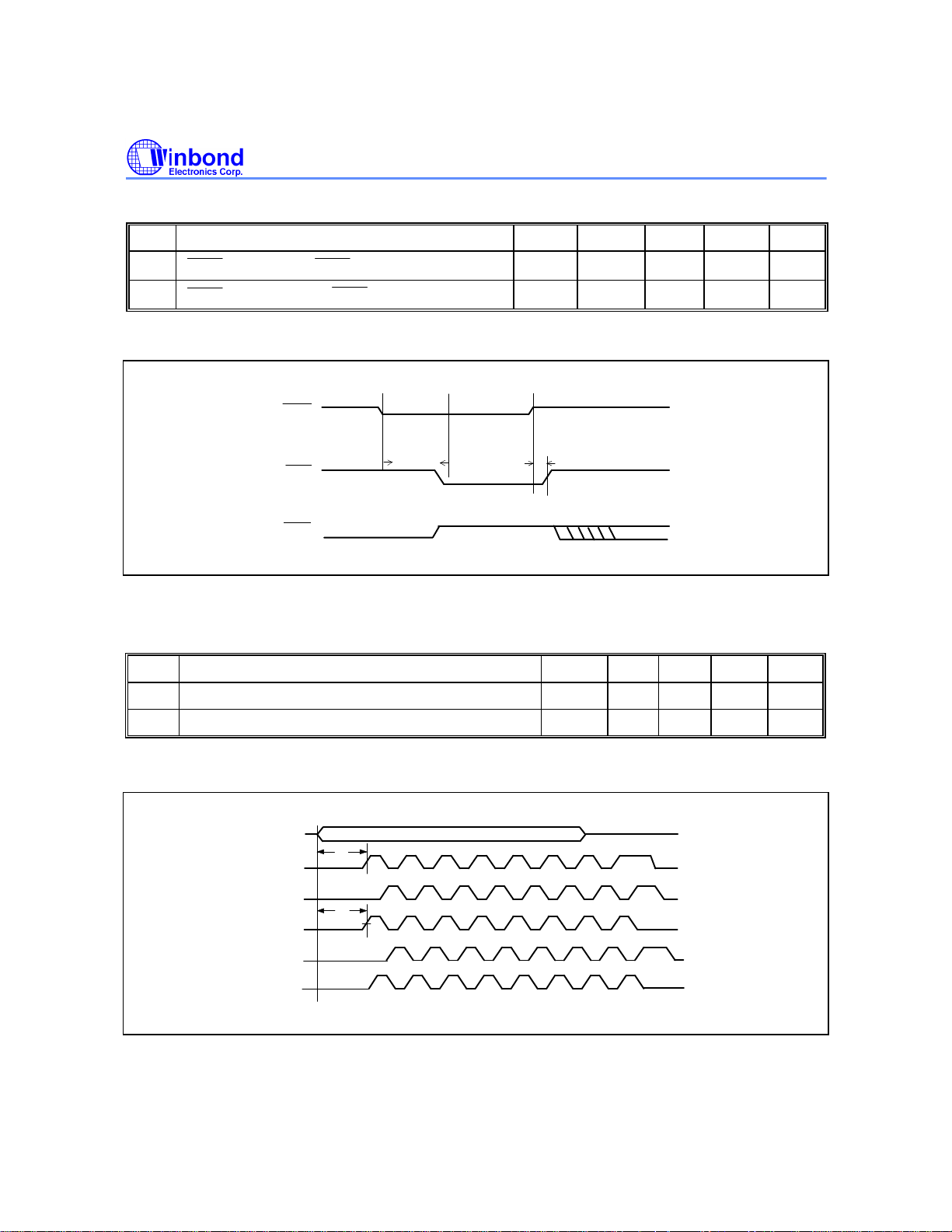
Inter-IMPR II Interface Collision Timing
NO. DESCRIPTION FIG. MIN. TYP. MAX. UNIT
1
2
asserted to
deasserted to
assertion
dessertion
Inter-IMPR II Interface Collision Timing Diagram
ICRS
7 35 nS
7 35 nS
ICOL
1
IBEN
Figure 7
2
Inter-IMPR II Interface to AUI/TP Port Timing
NO. DESCRIPTION FIG. MIN. TYP. MAX UNIT
1 Inter-IMPR II Interface to AUI Propagation Delay 8 5 Bits
2 Inter-IMPR II Interface to TP Propagation Delay 8 5 Bits
Inter-IMPR II Interface to AUI/TP port Timing Diagram
DT+
DD-
DD+
Figure 8
Publication Release Date: November 1996
- 23 - Revision A1
Page 24
Preliminary W89C982AF
312
DI+/-
DT+
DT-
DD-
DD+
IDAT
Valid Data
4
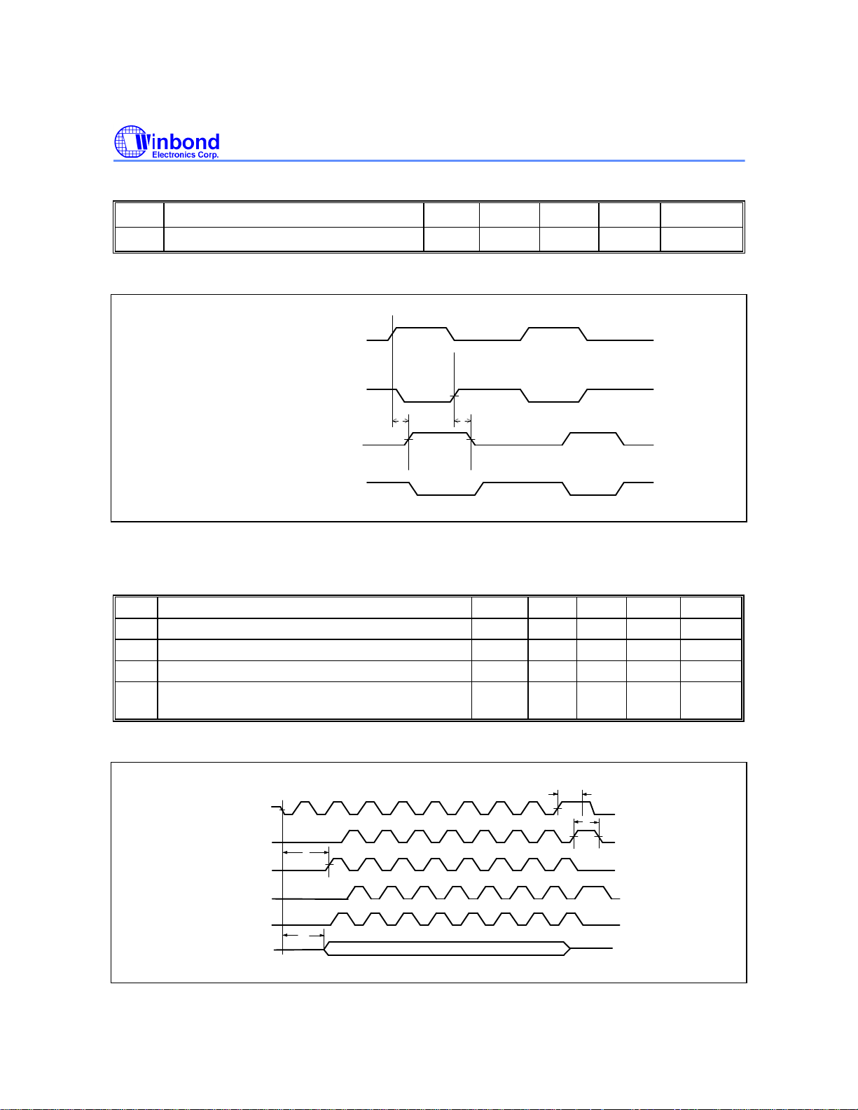
Output Driver Timing
NO. DESCRIPTION FIG. MIN. TYP. MAX. UNIT
1 DT+ to DD+ and DT- to DD- delay 9 47 53 nS
Output Driver Timing Diagram
Twister Pair Drivers
DT+
DT-
DD-
1
DD+
Figure 9
1
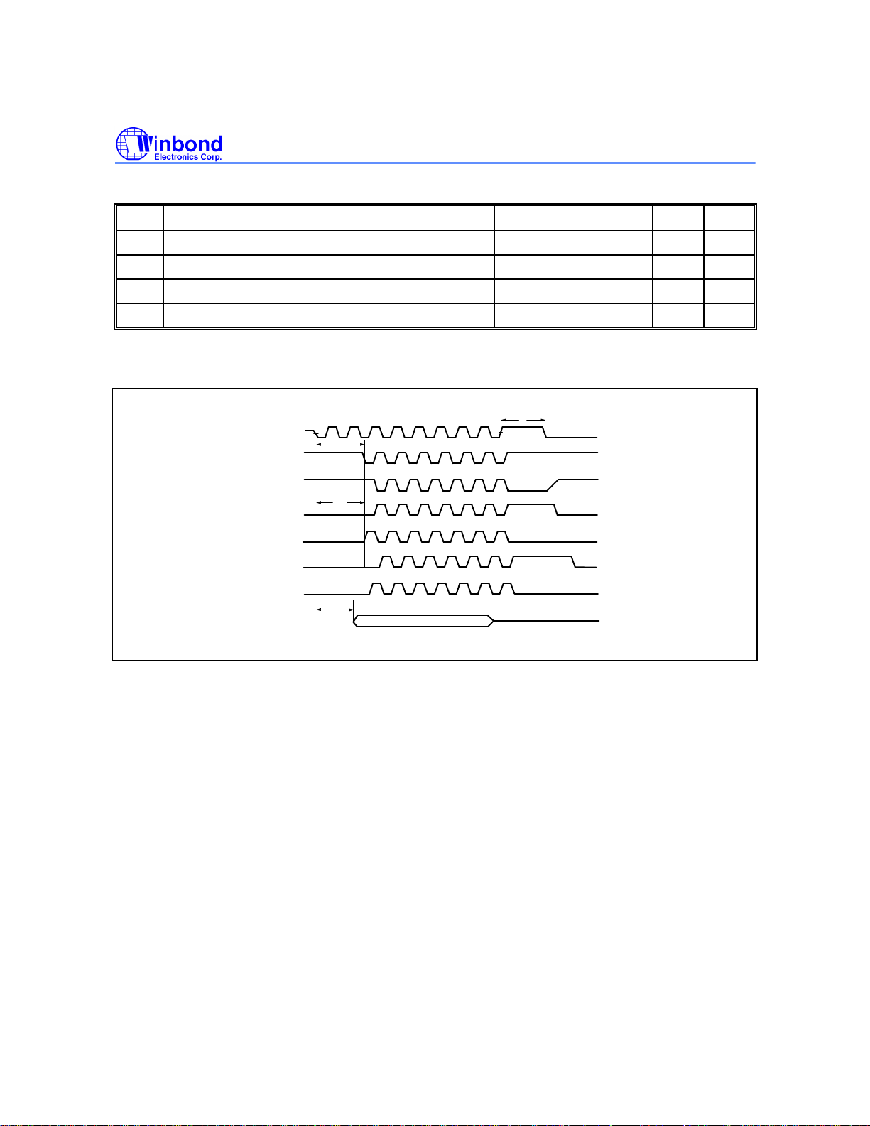
Repetition Timing (part 1)
NO. DESCRIPTION FIG. MIN. TYP. MAX. UNIT
1 Minimum AUI Start of Idle (SOI) Pulse Width 10 200 nS
2 Start of Idle Generated on Twisted Pair 10 250 300 350 nS
3 AUI to TP Propagation Delay 10 6 Bits
4 AUI to Inter-IMPR II interface Propagation
Delay
10 5 Bits
Repetition Timing Diagram (part 1)
Figure 10
- 24 -
Page 25
Preliminary W89C982AF
RD+/-
1
3
2
DO+
DO-
DT+
DT-
DD-
DD+
IDAT
Valid Data
4
Repetition Timing (part 2)
NO. DESCRIPTION FIG. MIN. TYP. MAX UNIT
1 Minimum Twisted Pair (SOI) Pulse Width 11 200 nS
2 TP to AUI Propagation Delay 11 7 Bits
3 TP to TP Propagation Delay 11 7 Bits
4 TP to Inter-IMPR II Interface Propagation Delay 11 6 Bits
Repetition Timing Diagram (part 2)
Figure 11
Publication Release Date: November 1996
- 25 - Revision A1
Page 26
Preliminary W89C982AF
27 uH
78 ohm
270 ohm
DO+
DO-
270 ohm
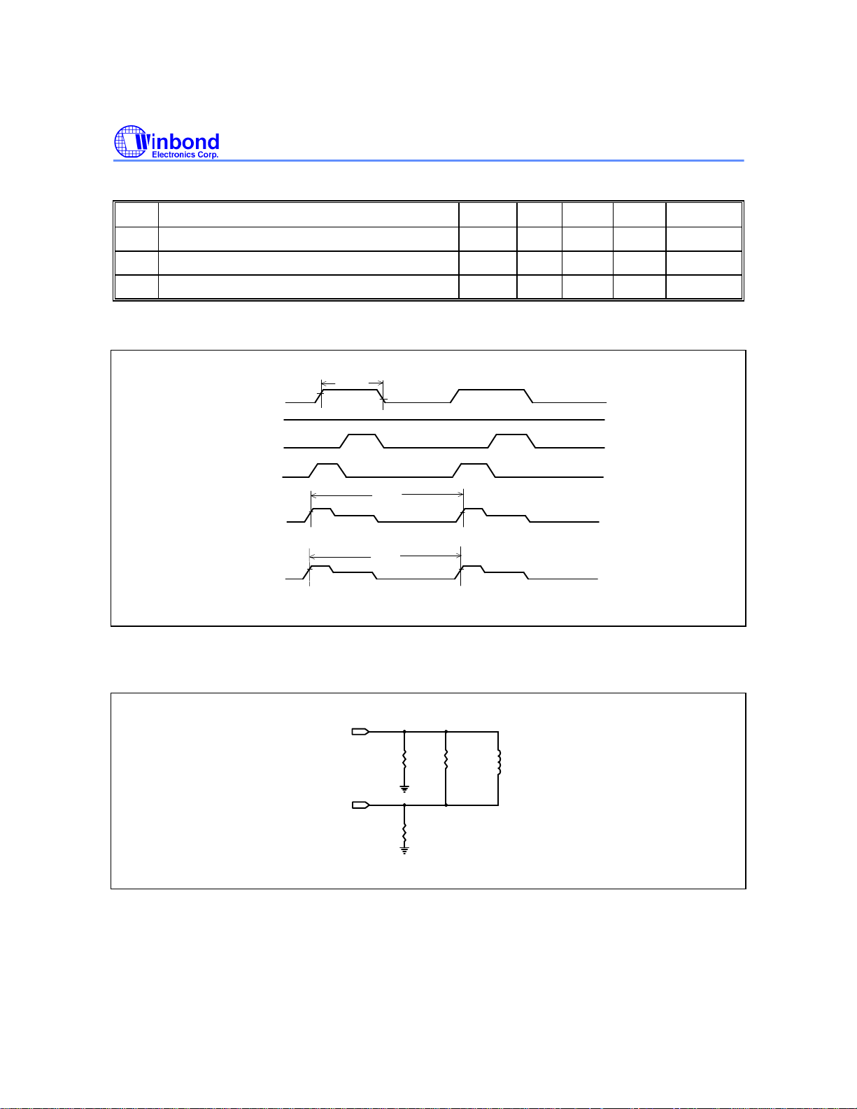
Link Test Timing
NO. DESCRIPTION FIG. MIN. TYP. MAX. UNIT
1 DT+ link pulse width 12 100 nS
2 Duration between transmitted link pulses 12 16 64 mS
3 Duration between received link pulses 12 3.8 64 mS
Link Test Timing Diagram
1
DT+
DT-
DD-
DD+
2
TX+/-
Transmitted Link Pulse
3
RX+/-
Received Link Pulse
AUI and DO+/- Switch Test Load
Figure 12
- 26 -
Page 27
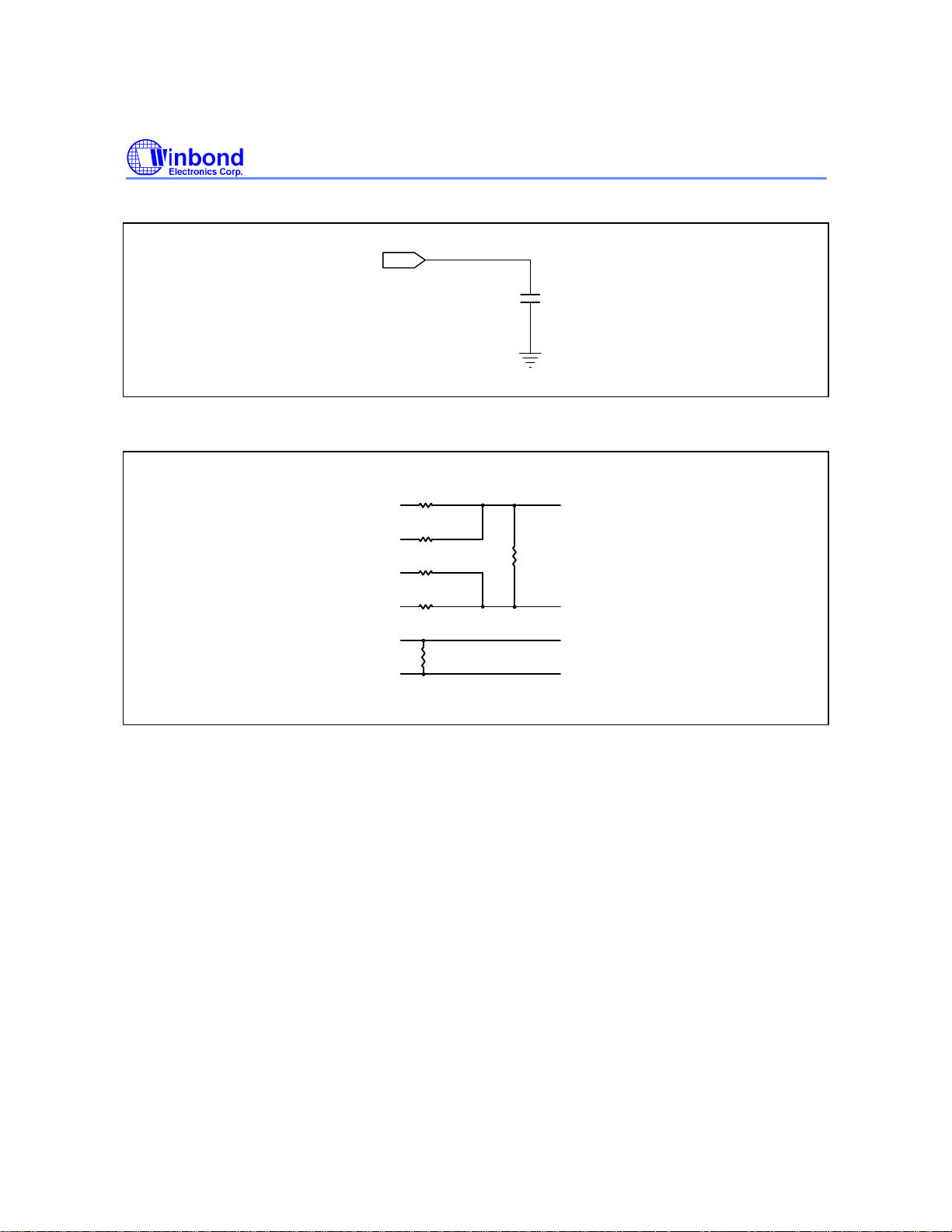
Digital Output Switching Test Load
Pre-equalization Network
Preliminary W89C982AF
50 pF
DTX+
DDX+
DTX-
DDX-
RDX+
RDX-
56 ohm
390 ohm
56 ohm
390 ohm
100 ohm
Tx+
1.21 Kohm
Tx-
Rx+
Rx-
Publication Release Date: November 1996
- 27 - Revision A1
Page 28
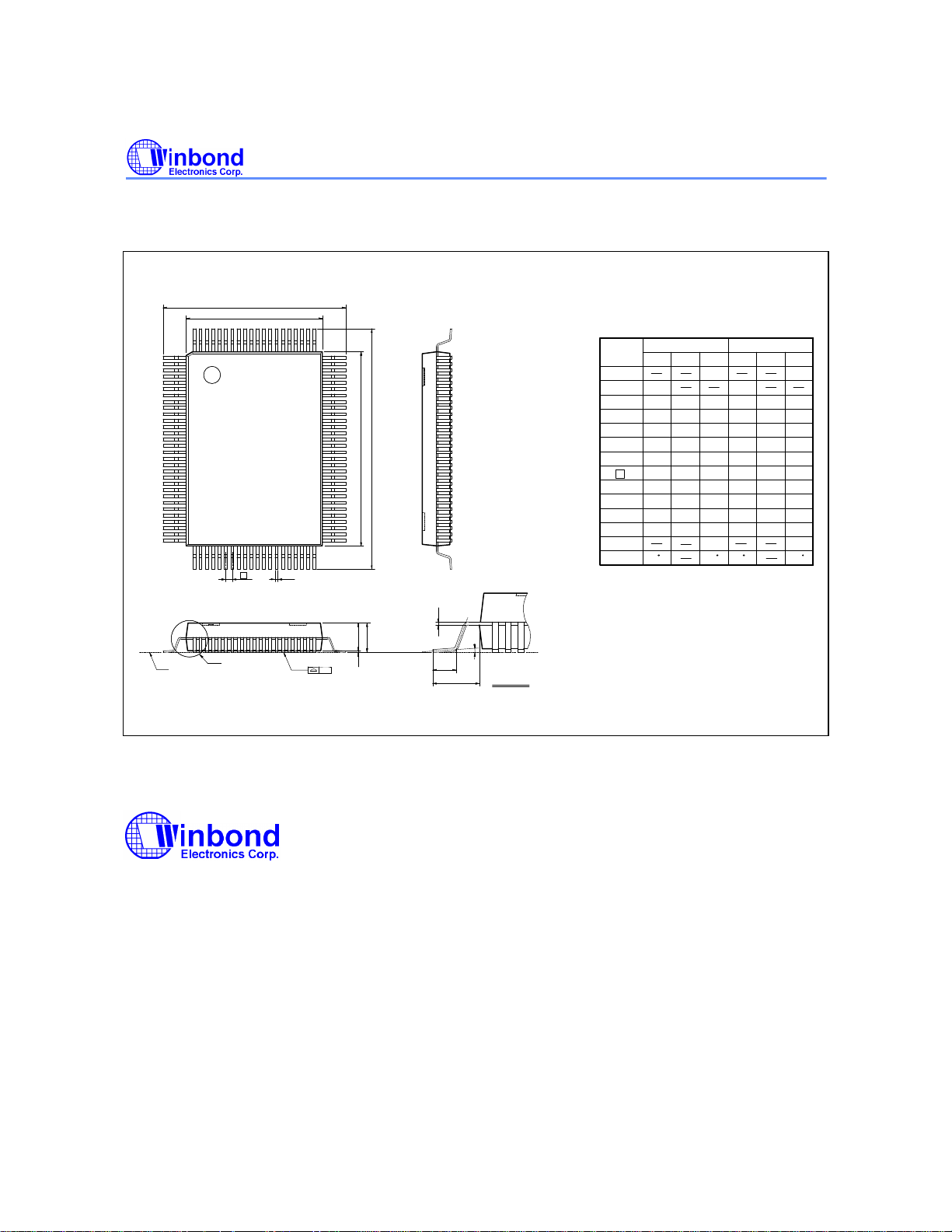
PACKAGE DIMENSIONS
Note: All data and specifications are subject to change without notice.
100-pin QFP
H
D
1
30
Seating Plane
D
e
See Detail F
81100
5031
b
y
Preliminary W89C982AF
Dimension in inches Dimension in mm
80
E
HE
51
c
AA
2
A
1
θ
L
L
1
Detail F
Symbol
A
A
1
2
A
b
c
D
E
e
D
H
H E
L
1
L
y
θ
Notes:
1. Dimension D & E do not include interlead
flash.
2. Dimension b does not include dambar
protrusion/intrusion.
3. Controlling dimension: Millimeters
4. General appearance spec. should be based
on final visual inspection spec.
Nom
Min
0.004
0.107
0.010
0.004
0.546
0.782
0.020
0.728
0.964
0.039
0.087
Max Max
0.130
0.117
0.112
0.016
0.012
0.006 0.152
0.010
0.556
0.551
0.792
0.787
0.026
0.032
0.752
0.740
0.988
0.976
0.055
0.047
0.095
0.103
0.004
Min
0.10
2.718
0.254
0.101
13.87
19.87
0.498 0.802
18.49
24.49
0.991
2.21 2.616
0120
Nom
3.30
2.972
2.845
0.407
0.305
0.254
14.00
14.13
20.00
20.13
0.65
19.10
18.80
24.80 25.10
1.397
1.194
2.413
0.102
12
Headquarters
No. 4, Creation Rd. III,
Science-Based Industrial Park,
Hsinchu, Taiwan
TEL: 886-3-5770066
FAX: 886-3-5792646
http://www.winbond.com.tw/
Voice & Fax-on-demand: 886-2-7197006
Taipei Office
11F, No. 115, Sec. 3, Min-Sheng East Rd.,
Taipei, Taiwan
TEL: 886-2-7190505
FAX: 886-2-7197502
Winbond Electronics (H.K.) Ltd.
Rm. 803, World Trade Square, Tower II,
123 Hoi Bun Rd., Kwun Tong,
Kowloon, Hong Kong
TEL: 852-27513100
FAX: 852-27552064
- 28 -
Winbond Electronics North America Corp.
Winbond Memory Lab.
Winbond Microelectronics Corp.
Winbond Systems Lab.
2727 N. First Street, San Jose,
CA 95134, U.S.A.
TEL: 1-408-9436666
FAX: 1-408-5441798
 Loading...