

Page 1

W88111AF/W88112F
ATAPI CD-ROM Decoder & Controller
This specification is subject to change without notice.
Preliminary/Confidential
Table Of Contents
GENERAL DESCRIPTION ________________________________________________________________5
BLOCK DIAGRAM_______________________________________________________________________6
PIN CONFIGURATION ___________________________________________________________________7
PIN DESCRIPTIONS______________________________________________________________________8
REGISTERS DESCRIPTION______________________________________________________________12
IR - Index Register (read/write) ____________________________________________________________12
PFAR - Packet FIFO Access Register - (read 00h) _____________________________________________12
INTCTL - Interrupt Control Register - (write 01h) _____________________________________________12
INTREA - Interrupt Reason Register - (read 01h) ______________________________________________ 13
TBCL/TBCH - Transfer Byte/Word Counter - (read/write 02h/03h) ________________________________15
TACL/TACH - Transfer Address Counter - (write 04h/05h) ______________________________________15
TBL/TBH - Transfer Block Register - (read/write 24h/25h) ______________________________________ 15
THTRG - Transfer to Host Trigger Register - (write 06h)________________________________________15
TACK - Transfer Acknowledge - (write 07h) __________________________________________________16
HEAD0 to HEAD3 - Header Registers - (read 03h to 07h)_______________________________________16
BIAL/BIAH - Buffering Initial Address Register - (write 08h/09h) _________________________________16
BACL, BACH - Buffering Address Counter - (read 0Ah/0Bh)_____________________________________16
EIAL/EIAH - ECC Initial Address Register- (read 08h/09h, write 0Ch/0Dh)_________________________16
SCBL/SCBH - Subcode Block Register - (read/write 26h/27h) ____________________________________17
DDBL/DDBH - Decoded Data Block Register - (read/write 28h/29h) ______________________________17
CTRL0 - Control Register 0 - (write 0Ah) ____________________________________________________17
CTRL1 - Control Register 1 - (write 0Bh) ____________________________________________________18
STAT0 - Status Register 0 - (read 0Ch) ______________________________________________________19
STAT1 - Status Register 1 - (read 0Dh) ______________________________________________________20
DHTACK - DRAM to Host Transfer Acknowledge - (write 0Eh) __________________________________21
STAT2 - Status Register 2 - (read 0Eh) ______________________________________________________ 21
FRST - Firmware Reset Register - (write 0Fh) ________________________________________________22
Publication Release Date: Aug, 1996
- 1 - Preliminary/Confidential Revision A0.1
Page 2

W88111AF/W88112F
ATAPI CD-ROM Decoder & Controller
This specification is subject to change without notice.
STAT3 - Status Register 3 - (read 0Fh) ______________________________________________________22
CTRLW - Control-Write Register - (write 10h) ________________________________________________ 23
STAT4 - Status Register 4 - (read 10h) ______________________________________________________24
CRTRG - Correction Retry Trigger - (write 11h) ______________________________________________24
MBTC0 - Multi-Block Transfer Control 0 - (read/write 12h) _____________________________________25
MBTC1 - Multi-Block Transfer Control 1 - (read/write 13h) _____________________________________26
ECTRL - Enhanced Control Register - (write 14h) _____________________________________________26
SUBH0 to SUBH3 - Subheader Registers - (read 14h to 17h) ____________________________________27
ASTRG - Automatic Sequence Trigger Register (write 17h) ______________________________________27
ASCTRL - Automatic Sequence Control register - (read/write 18h) ________________________________29
CCTL0 - Clock Control Register 0 - (write 19h) ______________________________________________31
CCTL1 - Clock Control Register 1 - (write 1Ah) _______________________________________________ 32
VER - Version Register - (read 1Ah) ________________________________________________________ 32
DSPSL - DSP Selection Register - (write 1Bh) ________________________________________________32
C2BEB - C2 Block Error Byte - (read 1Bh)___________________________________________________33
Preliminary/Confidential
RACL, RACH, and RACU - RAM Address Counter - (write 1Ch, 1Dh, 2Dh)_________________________ 33
RAMWR - RAM Write Register - (write 1Eh)__________________________________________________34
RAMRD - RAM Read Register - (read 1Eh) __________________________________________________34
HICTL0 - Host Interface Control Register - (write 1Fh)_________________________________________34
STAT5 - Status Register 5 - (read 1Fh) ______________________________________________________35
HICTL1 - Host Interface Control Register - (write 20h) _________________________________________36
SICTL0 - Subcode Interface Control Register 0 - (write 21h) ____________________________________37
SCIACK - Subcode Interrupt Acknowledge - (write 22h) ________________________________________ 37
SUBSTA - Subcode Status Register - (read 22h) _______________________________________________38
RAMCF - RAM Configuration Register - (read/write 2Ah)_______________________________________38
MEMCF - Memory Layout Configuration Register - (write 2Bh) __________________________________39
SICTL1 - Subcode Interface Control Register 1 - (write 2Ch) ____________________________________ 40
MISC0 - Miscellaneous Control Register 0 - (write 2Eh) ________________________________________41
MISS0 - Miscellaneous Status Register 0 - (read 2Eh) __________________________________________42
MISC1 - Miscellaneous Control Register 1 (write 2Fh) _________________________________________ 43
MISS1 - Miscellaneous Status Register 0 - (read 2Fh) __________________________________________ 44
ARSTACK - ATAPI Soft Reset Acknowledge (write 30h)_________________________________________ 45
MISS2 - Miscellaneous Status Register 0 (read 30h)____________________________________________46
Publication Release Date: Aug, 1996
- 2 - Preliminary/ Confidential Revision A0.1
Page 3

W88111AF/W88112F
ATAPI CD-ROM Decoder & Controller
This specification is subject to change without notice.
ATERR - ATAPI Error Register (write 31h)___________________________________________________47
ATFEA - ATAPI Feature Register (read 31h) _________________________________________________ 47
ATINT - ATAPI Interrupt Reason Register (read/write 32h) ______________________________________ 47
ATSPA - ATAPI SAM Tag Bytes Register (read/write 33h)_______________________________________48
ATBLO - ATAPI Byte Count Low (read/write 34h) _____________________________________________48
ATBHI - ATAPI Byte Count High (read/write 35h) _____________________________________________48
ATDRS - ATAPI Drive Select (read/write 36h) ________________________________________________ 48
ATSTA - ATAPI Status Register (read 38h, write 37h) __________________________________________ 48
ATCMD - ATAPI Command Register (read 37h)_______________________________________________48
ASSTA - ATAPI Shadow Status Register - (write 38h)___________________________________________49
ASERR - ATAPI Shadow Error Register - (write 39h)___________________________________________49
APKSTA - Status Register for Automatic Packet Transfer - (write 3Dh) ____________________________49
ASCSTA - Status Register for Automatic Status Completion - (write 3Eh) ___________________________49
SHDC - Shadow Drive Control Register _____________________________________________________50
DF0 to DF7 - uP to Host Data Transfer Registers - (write 40h to 47h) _____________________________ 50
Preliminary/Confidential
Ring Control Registers - (read/write 50h to 57h) ______________________________________________51
DTRBL/DTRBH - Data Transfer Ring Base Register - (read/write 50h/51h) _________________________51
DTRCL/DTRCH - Data Transfer Ring Ceiling Register - (read/write 52h/53h)_______________________51
WBRBL/WBRBH - Write Buffer Ring Base Register - (read/write 54h/55h)__________________________51
WBRCL/WBRCH - Write Buffer Ring Ceiling Register - (read/write 56h/57h) _______________________ 51
SCTC - Subcode Timer Control Register - (write 5Ah) __________________________________________51
TARCTL - Target Control Register - (write 80h)_______________________________________________52
TARSTA - Target Status Register - (read 80h)_________________________________________________52
DSTH/DSTL - Decoding Sector Threshold Register - (write 82h/81h) ______________________________53
DSCH/DSCL - Decoding Sector Counter - (read 82h/81h)_______________________________________53
TSL - Target Search Limit Register - (write 83h) ______________________________________________53
TSC - Target Search Counter - (read 83h)____________________________________________________54
Target Header Register - (read/write 84h-86h) ________________________________________________54
TMIN - Target Minute Register - (read/write 84h) _____________________________________________ 54
TSEC - Target Second Register - (read/write 85h) _____________________________________________ 54
TFRAM - Target Frame Register - (read/write 86h) ____________________________________________54
FEACTL - Feature Control Register - (write 88h)______________________________________________54
Status Mask Register - (write 8Ch-8Fh)______________________________________________________ 55
Publication Release Date: Aug, 1996
- 3 - Preliminary/ Confidential Revision A0.1
Page 4

W88111AF/W88112F
ATAPI CD-ROM Decoder & Controller
This specification is subject to change without notice.
STA0M - Status 0 Mask Register - (write 8Ch) ________________________________________________55
STA1M - Status 1 Mask Register - (write 8Dh) ________________________________________________ 55
STA2M - Status 2 Mask Register - (write 8Eh) ________________________________________________56
STA3M - Status 3 Mask Register - (write 8Fh) ________________________________________________56
REGISTER TABLE______________________________________________________________________57
D.C. CHARACTERISTICS________________________________________________________________ 61
PACKAGE DIMENSIONS ________________________________________________________________62
Preliminary/Confidential
Publication Release Date: Aug, 1996
- 4 - Preliminary/ Confidential Revision A0.1
Page 5

W88111AF/W88112F
ATAPI CD-ROM Decoder & Controller
This specification is subject to change without notice.
Preliminary/Confidential
GENERAL DESCRIPTION
The Winbond W88111AF/W88112F supports ATAPI CD-ROM specification (SFF 8020). Some
ATAPI operations are executed by hardware to minimize system overhead, including ATAPI
command and packet transfer, data transfer, ATAPI Soft Reset command, and Executive Drive
Diagnostics command. It also features shadow drive support.
The Winbond W88111AF/W88112F supports various types of microprocessors, DRAMs, and DSPs.
The W88111AF/W88112F supports up to 12/20-fold drive speed. It also supports CD-ROM, CD-
ROM/XA, CD-I, Video-CD, Photo-CD , and CD-Plus formats.
The functions of W88111AF/W88112F include CD-ROM data de-scrambling, real-time error
correction of Layer 3 Reed-Solomon Product-like Code (RSPC), error detection, and data transfer to
the host.
The W88111AF/W88112F features real-time ECC correction of one byte per P-word and Q-word. It
can also perform repeated ECC passes to increase the reliability of data.
The W88111AF/W88112F supports up to 1Mbytes of DRAM. It also supports ring-control-register to
add flexibility of external RAM control.
The host interface of W88111AF/W88112F supports data transfer using PIO, single word DMA, and
multi-word DMA modes. There is an 8-byte FIFO to improve the IDE interface throughput.
The W88111AF/W88112F supports multi-block-transfer from external RAM to the host.
* The W88112F supports accelerated error correction/detection to improve system performance.
* The W88112F supports automatic target header search, automatic header comparison, and decoder
interrupt status collection to reduce firmware overhead.
W88111AF/W88112F GENERAL FEATURES
⇒ Supports ATAPI CD-ROM standard (SFF 8020)
⇒ Supports CD-ROM, CD-ROM/XA, CD-I, Video-CD, Photo-CD, and CD-Plus formats
⇒ Supports drive speed up to 12-fold
⇒ Supports various types of microprocessors and DSPs
⇒ Supports various types of industry-standard DRAMs
⇒ Supports ring-control-register to add flexibility of DRAM control
⇒ Supports CD-ROM data descrambling
⇒ Supports real-time correction of one byte error per P-word and Q-word
⇒ Supports error detection of CD-ROM data
⇒ Supports repeated error correction and error detection passes
⇒ 8-byte FIFO to improve IDE interface throughput
⇒ Data transfer to host in PIO, single word DMA, and multi-word DMA modes
⇒ Multi-block transfer
⇒ 100-pin PQFP
Publication Release Date: Aug, 1996
- 5 - Preliminary/ Confidential Revision A0.1
Page 6
W88111AF/W88112F
ATAPI CD-ROM Decoder & Controller
This specification is subject to change without notice.
W88112F ENHANCED FEATURES
⇒ Supports drive speed up to 20-fold with 45ns DRAM
⇒ Up to 33% acceleration of error correction/detection
⇒ Automatic target header search
⇒ Automatic header comparison
⇒ Decoder interrupt status collection
⇒ Status valid timing control for high drive speed
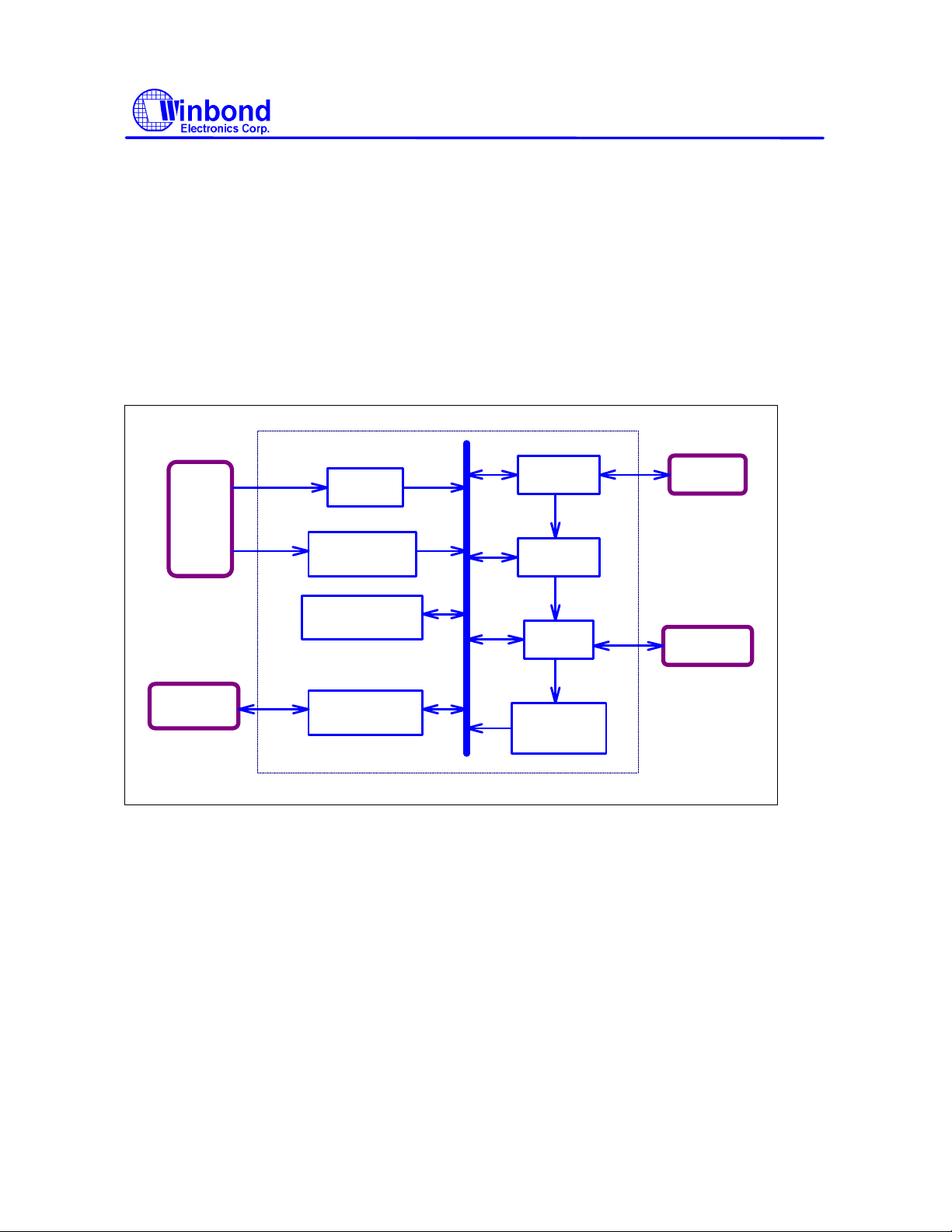
BLOCK DIAGRAM
Subcode
Interface
DSP
Sync Detector
& Descrambler
External RAM
Manager
Data FIFO
8 bytes
Preliminary/Confidential
DRAM
Micro-
Processor
ECC Corrector
& EDC Checker
Microprocessor
Interface
HOST
Interface
Command
Packet FIFO
12 bytes
ATAPI
Interface
Publication Release Date: Aug, 1996
- 6 - Preliminary/ Confidential Revision A0.1
Page 7
W88111AF/W88112F
ATAPI CD-ROM Decoder & Controller
This specification is subject to change without notice.
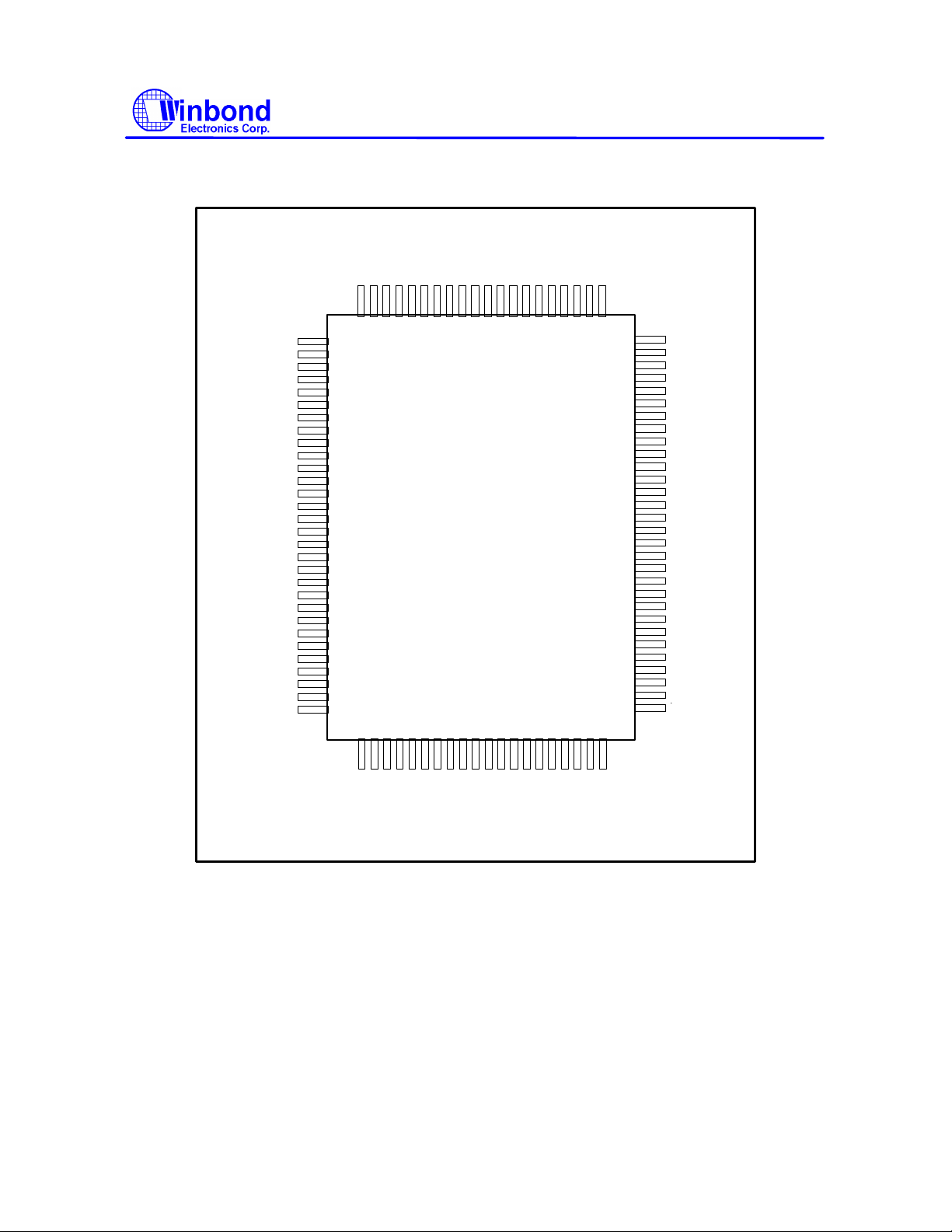
PIN CONFIGURATION
R
R
A
A
1
2
GND
RA3
RA11
RA12
RA13
RA15
NC
LRCK
SDATA
BCK
C2PO
PAR/DJ
CLKO
XOUT
XIN
GND
SCSB
WFCK
SCSYN
EXCK
HRSTb
UD0
UD1
NC
UD2
UD3
UD4
UD5
UD6
GND
0
1
0
2
3
4
5
6
7
8
9
10
11
12
13
14
15
16
17
18
19
20
21
22
23
24
25
26
27
28
29
30
313233343536373839404142434445464748495
R
A
A
A
5
4
0
R
R
N
A
A
A
A
D
9
7
6
8
G
R
R
R
R
W88111AF
/W88112F
Preliminary/Confidential
R
R
A
R
V
W
D
D
1
E
1
D
4
b
R
R
R
R
A
R
O
N
D
C
0
D
D
1
E
3
2
0
b
818283848586878889909192939495969798991
80
79
78
77
76
75
74
73
72
71
70
69
68
67
66
65
64
63
62
61
60
59
58
57
56
55
54
53
52
51
0
GND
RD6
RD7
RD5
RD4
CRSTb
DD7
DD8
NC
DD6
DD9
DD5
DD10
DD4
GND
DD11
NC
DD3
DD12
DD2
ARSTb
DD13
NC
DD1
DD14
DD0
DD15
DMARQ
HWR
GND
U
U
U
U
U
U
D
C
D
R
R
W
7
C
S
D
R
S
b
b
b
C
I
A
S
S
S
N
3
1
P
T
b
b
b
b
P
D
V
D
D
I
G
H
I
D
D
A
D
A
A
O
N
I
2
D
0
1
C
D
A
S
G
1
b
6
b
H
I
O
M
R
R
R
A
D
Q
D
C
b
Y
K
b
Publication Release Date: Aug, 1996
- 7 - Preliminary/ Confidential Revision A0.1
Page 8

W88111AF/W88112F
ATAPI CD-ROM Decoder & Controller
This specification is subject to change without notice.
PIN DESCRIPTIONS
The following convention is used in the pin description table below:
• (I) denotes an input
• (O) denotes an output
• (OZ) denotes a tri-state output
• (OD) denotes an open-drain output
• (I/O) denotes a bi-directional signal
Miscellaneous Pins
NAME NO. TYPE PIN DESCRIPTION
PAR/PJ
CLKO
XIN
XOUT
HRSTb
ARSTb
CRSTb
VDD
GND
NC
12
13
15
14
21
60
75
41, 89
1, 16, 30, 46,
51, 66, 80, 94
7, 24, 58, 64,
72, 86
I/O RAM Parity Data/Drive Jumper - As a RAM parity bit when
PJSEL (19h.6) is high and as a drive select jumper when PJSEL
is low.
O Clock Output - If CLKOS (1Ah.3) is low, CLKO pin will supply
clock signal of one-half the crystal frequency. If CLKOS is high,
CLKO pin will supply normal crystal frequency.
I
Crystal Input/Output - Normally, XIN and XOUT are connected to
a crystal.
O
I Host Reset - A pin receives reset signal from the host.
OD ATAPI Reset - After receiving an ATAPI Soft Reset command,
this pin becomes active-low when ARSTEN (2Fh.3) is enabled.
I Chip Reset - Forcing this input low to reset the whole chip.
Power Supply Pin - 5.0V ± 5%
Ground Pin
No Connected Pin
Preliminary/Confidential
Micro-controller Interface
NAME NO. TYPE PIN DESCRIPTION
UD[7:0]
URS
URDb
UWRb
UCSb
22, 23, 25, 26,
27, 28, 29, 31
32
33
34
35
I/OZ Microprocessor Data Bus - Bi-directional processor data lines.
I Register Select - To select address register or internal register.
I Microprocessor Read Strobe - A low-active signal.
I Microprocessor Write Strobe - A low-active signal.
I Microprocessor Chip Select - A low-active signal.
- 8 - Preliminary/ Confidential Revision A0.1
Publication Release Date: Aug, 1996
Page 9

W88111AF/W88112F
ATAPI CD-ROM Decoder & Controller
This specification is subject to change without notice.
UINTb
36
OD Microprocessor Interrupt - A signal can be externally wired-OR
Host Interface
NAME
DD[15:0]
DA[2:0]
DASPb
CS3b
CS1b
PDIAGb
IOCS16b
HIRQ
DMACKb
IORDY
HRDb
HWRb
DMARQ
NO.
54, 56, 59, 62,
65, 68, 70, 73,
74, 71, 69, 67,
63, 61, 57, 55
40, 44, 42
37
38
39
43
45
47
48
49
50
52
53
TYPE PIN DESCRIPTION
I/OZ Host Data Bus - Signals enable data transfer between the host
I Host Address Bus - Signals to access various ATAPI registers.
I/OD Drive Active/Drive 1 Present - A time-multiplexed signal
I Host Chip Select 1 - A signal used to select the host Control
I Host Chip Select 0 - A signal used to select the host Command
I/OD Passed Diagnostics - A signal asserted by Drive 1 to indicate to
OD 16-bit I/O Select - During PIO transfer, this signal becomes
OZ Host Interrupt - A signal to request an interrupt service from
I DMA Acknowledge - A signal used for DMA transfer by the host
OZ I/O Channel Ready - When W88111AF/W88112F is not ready
I Host I/O Read - The read strobe signal.
I Host I/O Write - The write strobe signal.
OZ DMA Request - A signal asserted for DMA data transfer when
Preliminary/Confidential
with other interrupt sources.
and W88111AF/W88112F.
indicating whether a drive is active, or Drive 1 is present.
Block Registers.
Block Registers.
Drive 0 that diagnostics is completed.
active-high to indicate a 16-bit data transfer.
host.
when DMARQ is ready.
for a data transfer request, this signal is negated for extension of
the host data transfer cycle within any host register access.
W88111AF/W88112F is ready to transfer data to or from the
host.
ATAPI Register Definition
ADDRESSES FUNCTIONS
CS1b CS3b DA2 DA1 DA0 Read Write
Control block registers
N A 1 1 0 Alternate status Device control
Publication Release Date: Aug, 1996
- 9 - Preliminary/ Confidential Revision A0.1
Page 10

W88111AF/W88112F
ATAPI CD-ROM Decoder & Controller
This specification is subject to change without notice.
Command block registers
A N 0 0 0 Data
A N 0 0 1 ATAPI Error Register ATAPI Features
A N 0 1 0 ATAPI Interrupt Reason Register
A N 0 1 1 Reserved for SAM TAG Bytes
A N 1 0 0 ATAPI Byte Count Register (bits 0-7)
A N 1 0 1 ATAPI Byte Count Register (bits 8-15)
A N 1 1 0 Drive Select
A N 1 1 1 ATAPI Status ATA Command
Note : A = signal asserted, N = signal negated
Preliminary/Confidential
DSP Interface
NAME NO. TYPE PIN DESCRIPTION
LRCK 8 I L/R Channel Clock - Left and right channels are distinguished by
this signal.
SDATA 9 I Serial Data - Serial data from DSP is received from this input.
BCK 10 I Bit Clock - Bit clock from DSP is received from this input.
C2PO 11 I C2 Pointer - C2 error flag from DSP is received from this input.
Subcode Interface
NAME NO. TYPE PIN DESCRIPTION
SCSD 17 I Subcode Serial Data - Subcode serial data from DSP is
received from this input.
WFCK 18 I Write Frame Clock - Write frame clock from DSP is received
from this input.
SCSYN 19 I Subcode Sync - Subcode sync from DSP is received from this
input.
EXCK 20 I/O External Clock - A pin programmed as input or output to supply
bit clock for subcode.
External RAM Interface
NAME NO. TYPE PIN DESCRIPTION
ROEb
RWEb
84
88
O External RAM Output Enable - External RAM read strobe.
O External RAM Write Enable - External RAM write strobe.
Publication Release Date: Aug, 1996
- 10 - Preliminary/ Confidential Revision A0.1
Page 11

W88111AF/W88112F
ATAPI CD-ROM Decoder & Controller
This specification is subject to change without notice.
RD[7:0]
RA[9:0]
RA[13:10]
RA[15:14]
78, 79, 77, 76,
81, 82, 87, 85
91, 92, 93, 95,
96, 97, 2, 100,
99, 98
5, 4, 3, 83
6, 90
I/O RAM Data Bus - Data bus for external RAM.
O RAM Address Bus - Address bus for external RAM.
O External RAM Column Address Strobe - External RAM column
O External RAM Row Address Strobe - External RAM row
Preliminary/Confidential
address strobe.
address strobe.
Publication Release Date: Aug, 1996
- 11 - Preliminary/ Confidential Revision A0.1
Page 12

W88111AF/W88112F
ATAPI CD-ROM Decoder & Controller
This specification is subject to change without notice.
Preliminary/Confidential
REGISTERS DESCRIPTION
IR - Index Register (read/write)
When URS(pin 32) is low, the Index Register can be accessed by the microprocessor. The value in
IR specifies which internal register to be accessed by microprocessor when URS(pin 32) is high. Note
that the 4 least significant bits of IR will increase following each read or write to any register except
for PFAR(00h). Since IR does not automatically increase from 00h to 01h, consecutive reads to
address 00h will repeatedly read register PFAR(00h). This feature accelerates read operation of
ATAPI Command Packet.
PFAR - Packet FIFO Access Register - (read 00h)
While SCoD(20h.2) is high, the ATAPI Command Packet issued from host is received by the 12-byte
Packet FIFO. Flag TENDb(01h.6) is used to check if the Packet FIFO is full. The microprocessor
can read the ATAPI Command Packet by repeatedly read register PFAR(00h). Once the FIFO
becomes empty, the value FFh will be returned if microprocessor read PFAR.
The Packet FIFO can also be used to receive command parameter less than 12 bytes. First, the
control bit SCoD(20h.2) is set high to select the Packet FIFO to be addressed by the ATAPI Data
port. When DRQ(37h.3) changes from 0 to 1, the lower 4 bits of ATBLO(34h) is latched as the FIFO
threshold. Upon the number of bytes in the FIFO reaches the threshold, flag TENDb(01h.6) becomes
active-low and flag FPKT(30h.1) becomes active-high. Once FPKT becomes high, any data writes to
the ATAPI Data port is rejected.
INTCTL - Interrupt Control Register - (write 01h)
Bit 7: PFNEEN - Packet FIFO Not Empty Interrupt Enable
UINTb(pin 36) is activated when PFNEb(01h.7) becomes active-low if this bit is high.
Bit 6: TENDEN - Transfer End Interrupt Enable
UINTb(pin36) is activated when TENDb(01h.6) becomes active-low if this bit is high. TENDEN is
also automatically enabled if the host issues the Packet Command(A0h) while HIIEN(2Eh.7) is
high and drive is selected.
Bit 5: SRIEN - Sector Ready Interrupt Enable
UINTb(pin36) is activated when SRIb(01h.5) becomes active-low if this bit is high.
Publication Release Date: Aug, 1996
- 12 - Preliminary/ Confidential Revision A0.1
Page 13

W88111AF/W88112F
ATAPI CD-ROM Decoder & Controller
This specification is subject to change without notice.
Preliminary/Confidential
Bits 4, 3, 2: Reserved
Bit 1: DTEN - Data Transfer Enable
Set DTEN high enables the data transfer logic. This bit should be set before any of the following
data transfers is triggered:
• Host write to the Packet FIFO
• Host read from external RAM
• Host read from DF0 to DF7
In order to reduce the interference of microprocessor, DTEN is also automatically enabled during
the following operation:
• Trigger ADTT(17h.2)
• Host issues ATAPI Packet Command(A0h) while APKTEN(18h.7) is enabled and drive is
selected
Bit 0: Reserved
INTREA - Interrupt Reason Register - (read 01h)
Bit 7: PFNEb - Packet FIFO Not Empty Interrupt Flag
This bit becomes active-low after Packet FIFO receives any data issued by the host through
ATAPI Data port. UINTb(pin 36) is activated when PFNEb becomes active-low if PFNEEN(01h.7)
is enabled. PFNEb is deactivated after the last byte is read by microprocessor through register
PFAR(00h).
Bit 6: TENDb - Transfer End Interrupt Flag
This bit becomes active-low at the end of the following data transfers:
• Host writes to the Packet FIFO
• Host read from external RAM
• Host read from registers DF0(40h) to DF7(47h)
Flags TDIR(30h.5) and FPKT(30h.1) can be used to determine which type of transfer end occurs.
UINTb(pin36) is activated when TENDb becomes active-low if TENDEN(01h.6) is enabled.
Writing any value to register TACK(07h) deactivates this flag.
Bit 5: SRIb - Sector Ready Interrupt Flag
This bit is used to indicate that one sector is ready to be accessed. Reading register STAT3(0Fh)
deactivates SRIb.
Publication Release Date: Aug, 1996
- 13 - Preliminary/ Confidential Revision A0.1
Page 14

W88111AF/W88112F
ATAPI CD-ROM Decoder & Controller
This specification is subject to change without notice.
Preliminary/Confidential
Bit 4: HCIb - Host Command Interrupt Flag
This bit is activated by the following events:
• Host issues ATAPI Soft Reset Command, if ARSTIEN(2Fh.1) is enabled
• Host issues command to a non-exist slave drive, if SHIEN(2Eh.2) is enabled
• Host issues Execute Drive Diagnostics Command, if HIIEN(2Eh.7) is enabled
• ATAC(2Fh.6) becomes active-high, if HIIEN(2Eh.7) is enabled
• Host set bit SRST in ATAPI Device Control Register, if HIIEN(2Eh.7) is enabled
Bit 3: TBSYb - Transfer Busy Flag
This bit becomes active-low when the data transfer to host is triggered by the following events:
• Writing any value to register THTRG(06h)
• Setting bit ADTT(17h.2) high
After host reads the last byte to be transferred, TBSYb is deactivated.
Bit 2: MBTIb - Multi-Block Transfer Interrupt Flag
This bit is activated by the following events:
• RPINT(30h.3) becomes active-high while RPIEN(2Ah.5) is enabled
• MBTI(30h.4) becomes active-high while MBKIEN(13h.2) is enabled
The microprocessor can read register MISS2(30h) to tell which event occurs.
Bit 1: DFRDYb - Data FIFO Ready
After data transfer is triggered, the 8-byte Data FIFO is automatically filled. This bit is used to
indicate that the Data FIFO is ready to be read by the host.
Bit 0: SCIb - Subcode Interrupt Flag
If SCIEN(2Ch.4) is enabled, this bit becomes active-low when one of the following events occurs:
• ISS(22h.0) becomes active-high
• NESBK(22h.1) becomes active-high
• MSS(22h.2) becomes active-high
When Subcode Interrupt is activated, the microprocessor can read register SUBSTA(22h) to
determine the reason of interrupt. Writing register SCIACK(22h) deactivates Subcode Interrupt.
Publication Release Date: Aug, 1996
- 14 - Preliminary/ Confidential Revision A0.1
Page 15

W88111AF/W88112F
ATAPI CD-ROM Decoder & Controller
This specification is subject to change without notice.
Preliminary/Confidential
TBCL/TBCH - Transfer Byte/Word Counter - (read/write 02h/03h)
Before triggering data transfer, the number of bytes or words to be transferred should be set through
12-bit Transfer Byte/Word Counter. The number of bytes minus 1 should be written to this counter
while using 8-bit data transfer. The number of words minus 1 should be written to this counter while
using 16-bit data transfer. After host reads one byte or word, the counter is decreased by one till
Transfer End Interrupt is activated when this counter becomes zero.
TACL/TACH - Transfer Address Counter - (write 04h/05h)
Before triggering data transfer, the external RAM address of data to be transferred should be set
through 16-bit Transfer Address Counter. This number in this counter specifies the first available
data address relative to the beginning of the block. The block number should also be specified
through Transfer Block registers TBL/TBH(24h/25h). After one byte/word is read by host,
TACL/TACH are increased to the next available data address.
TBL/TBH - Transfer Block Register - (read/write 24h/25h)
Before triggering data transfer, the external RAM block of data to be transferred should be set through
Transfer Block Registers. TBL/TBH form a 9-bit register that is used to specify the first RAM block to
be transferred, while TACL/TACH(04h/ 05h) specify the starting address relative to the beginning of
this RAM block. The RAM block number in TBL/TBH is not increased automatically at the end of
each transfer unless multi-block transfer is used by specifying register MBTC0(12h).
THTRG - Transfer to Host Trigger Register - (write 06h)
This register is used to trigger data transfer regardless of what value is written.
When bit UDTS(1Fh.6) is low, the data transfer from external RAM to the host after THTRG is
triggered. Triggering THTRG automatically fills the Data FIFO and then flag DFRDYb(01h.1)
becomes active-low when the Data FIFO becomes ready.
When bit UDTS(1Fh.6) is high, the path of data transfer is from registers DF0-DF7(40h-47h) to the
host. In this case, the data count, less than 8, should be set using registers TBCL(02h) before
triggering THTRG and bit UDTT(1Fh.7) should be set to 1 followed by 0 after triggering THTRG.
Publication Release Date: Aug, 1996
- 15 - Preliminary/ Confidential Revision A0.1
Page 16

W88111AF/W88112F
ATAPI CD-ROM Decoder & Controller
This specification is subject to change without notice.
Preliminary/Confidential
TACK - Transfer Acknowledge - (write 07h)
Writing register TACK deactivates TENDb(01h.6) and its corresponding microprocessor interrupt
regardless of what data is written.
HEAD0 to HEAD3 - Header Registers - (read 03h to 07h)
These four registers are used to hold the information of Header Bytes of each sector. Header
Registers should be read soon after STAVAb(0F.7) becomes active-low. Note that the header bytes
are untrustful if wrong mode is set while ECC is enabled. If the bit SHDEN(0Bh.0) is enabled,
registers HEAD0-3 are used to hold subheader bytes instead.
BIAL/BIAH - Buffering Initial Address Register - (write 08h/09h)
Before enabling the external RAM buffering, BIAL/BIAH should be set to control the location of the
first byte follows data sync for each data sector. The RAM block for buffering is controlled by the
number in registers DDBL/DDBH(28h/29h) plus one. For convenience of following data transfer, the
microprocessor should set proper value to BIAH/BIAL(FF,F0h for mode-1 and FF,E8h for mode-2)
after the mode is determined so that the first user data byte will locate at offset 00h of each data
block.
BACL, BACH - Buffering Address Counter - (read 0Ah/0Bh)
After enabling the external RAM buffering, Buffering Write Counter are automatically increased by
two , beginning from the value specified by BIAL/BIAH, every time a data word is buffered.
EIAL/EIAH - ECC Initial Address Register- (read 08h/09h, write 0Ch/0Dh)
EIAL/EIAH are used to hold the initial address offset of the data block to be corrected. The content of
BIAL/BIAH(08h/09h) will be automatically loaded to EIAL/EIAH at the beginning of each data sync,
making it unnecessary to read or write EIAL/EIAH during normal operation. The RAM block for ECC
is controlled by the number in registers DDBL/DDBH(28h/29h).
Publication Release Date: Aug, 1996
- 16 - Preliminary/ Confidential Revision A0.1
Page 17

W88111AF/W88112F
ATAPI CD-ROM Decoder & Controller
This specification is subject to change without notice.
Preliminary/Confidential
SCBL/SCBH - Subcode Block Register - (read/write 26h/27h)
SCBL/SCBH form a 9-bit register that contains a block number of the latest available subcode data
that can be read by the host. The number in SCBL/SCBH plus 1 points to the RAM block that is
buffering incoming subcode. The number in SCBL/SCBH is increased by one at the end of subcode
block buffering.
DDBL/DDBH - Decoded Data Block Register - (read/write 28h/29h)
DDBL/DDBH form a 9-bit register that contains the number of the latest available decoded data block
after decoder interrupt occurs. This block number should be used to specify TBL/TBH(24h/25h)
before triggering data transfer to the host. This decoded-data-block-number plus 1 points to the
DRAM block that is buffering incoming serial data and increases by one at the end of each data block
buffering.
CTRL0 - Control Register 0 - (write 0Ah)
Bit 7: DECEN - Decoding Logic Enable
Setting this bit high enables the decoding logic.
Bit 5: EDCEN - Error Detect and Correct Enable
Setting this bit high enables the ECC and EDC logic.
Bit 4: ACEN - Automatic Correction Enable
When this bit is set high during MODE 2 ECC, the type of error correction is automatically
determined by the setting of the FORM bit in the subheader byte. When this bit is low during
MODE 2 ECC, the type of error correction is controlled by F2RQ(0Bh.2).
Bit 2: BUFEN - Buffering Enable
Setting this bit high enables incoming DSP data buffering. When this bit is high, the values of
register HEAD0-3(04h-07h) and SUBH0-3(14h-17h) are retrieved from external RAM rather than
from incoming serial data. When BUFEN is low, any setting of QCEN or PCEN is meaningless.
Bit 1: QCEN - Q-codeword Correction Enable
When this bit is high, Q-codeword RSPC correction logic is enabled.
Publication Release Date: Aug, 1996
- 17 - Preliminary/ Confidential Revision A0.1
Page 18

W88111AF/W88112F
ATAPI CD-ROM Decoder & Controller
This specification is subject to change without notice.
Bit 0: PCEN - P-codeword Correction Enable
When this bit is high, P-codeword RSPC correction logic is enabled.
Bit 6,3: Reserved
DECEN
0Ah.7
1 1 1 1 1 Q-P correction
1 1 1 1 0 Q-correction
1 1 1 0 1 P-correction
1 1 1 0 0 Write-only CRC
1 0 0 0 0 Disk-monitor no buffering
0 X X X X Decoder
BUFEN
0Ah.2
EDCEN
0Ah.5
QCEN
0Ah.1
PCEN
0Ah.0
Decoder
Mode
disable
Preliminary/Confidential
Operation
Flow
Q → P → CRC
Q → CRC
P → CRC
no operation
CTRL1 - Control Register 1 - (write 0Bh)
Bit 7: SIEN - Sync Insertion Enable
When this bit is high, the sector boundary is determined by internal sync insertion logic.
Bit 6: SDEN - Sync Detection Enable
When this bit is high, the sector boundary is determined by incoming serial data.
Bit 5: DSCREN - Descrambler Enable
Setting this bit high enables the descrambling logic.
Bit 4: CWEN - Corrected Data Write Enable
Setting this bit high enables corrected data to be written to the external RAM.
Bit 3: M2RQ - Mode 2 ECC Request
Setting this bit high enables the mode 2 ECC correction logic. Mode 1 ECC correction will be
performed if this bit is low.
Publication Release Date: Aug, 1996
- 18 - Preliminary/ Confidential Revision A0.1
Page 19

W88111AF/W88112F
ATAPI CD-ROM Decoder & Controller
This specification is subject to change without notice.
Preliminary/Confidential
Bit 2: F2RQ - Form 2 Request
Setting this bit high requests the data to be processed by the mode-2 form-2 format if
M2RQ(0Bh.3) is high.
Bit 1: MCRQ - Mode Byte Check Request
When this bit is high, ECC logic will check the 4th header byte with the setting of M2RQ(0Bh.3) to
determine if ECC correction needs to be performed.
Bit 0: SHDEN - Subheader Switch Enable
When this bit is high, registers HEAD0-3 are used to provide subheader bytes.
STAT0 - Status Register 0 - (read 0Ch)
Bit 7: CRCOK - Cyclic Redundancy Check OK
This bit is used to indicate whether the Cyclic Redundancy Check of the latest available sector is
passed.
Bit 6: ILSYN - Illegal Sync Pattern
If SDEN(0Bh.6) is high, this bit becomes high when a sync pattern is detected less than 2352
bytes after last sync pattern was detected/inserted.
Bit 5: NOSYN - No Sync Pattern
If SIEN(0Bh.7) is high, this bit becomes high when a sync pattern is not detected at 2352 bytes
after last sync pattern was detected/inserted.
Bit 4: LBKF - Long Block Flag
If SIEN(0Bh.7) is low, this bit becomes high when a sync pattern is not detected at 2352 bytes
after last sync pattern was detected/inserted.
Bit 3: WSHORT - Word Short
This bit becomes high when the incoming serial data rate is too high to be processed by
W88111AF/W88112F.
Bit 2: SBKF - Short Block Flag
If SDEN(0Bh.6) is low, this bit becomes high when a sync pattern is detected less than 2352 bytes
after last sync pattern was detected/inserted.
Publication Release Date: Aug, 1996
- 19 - Preliminary/ Confidential Revision A0.1
Page 20

W88111AF/W88112F
ATAPI CD-ROM Decoder & Controller
This specification is subject to change without notice.
Status Flag
ILSYN(0Ch.6) x 1 re-synchronize internal sync logic
NOSYN(0Ch.5) 1 x internal sync logic provide internal sector
LBKF(0Ch.4) 0 x internal sync logic do not provide internal
SBKF(0Ch.2) x 0 do not re-synchronize internal sync logic
SIEN
(0Bh.7)
SDEN
(0Bh.6)
Internal Operation
boundary
sector boundary
Preliminary/Confidential
Bit 1: FDIF - Fast Decoder Interrupt Flag
If FDIEN(10h.3) is enabled, this bit becomes high when the Header/Subheader bytes are ready
after ECC is complete and before CRC is complete. Meanwhile, UINTb(pin 36) and
STAVAb(0Fh.7) become active-low thus accelerate the following microprocessor operations.
FDIF is deactivated when CRC is complete. UINTb(pin 36) also becomes low-active when CRC is
complete. So if FDIEN(10h.3) is enabled, CRCVAb(10h.7) should be used to determine whether
the CRCOK(0Ch.7) is available when interrupt becomes active.
Bit 0: UEBK - Incorrectable Errors in Block
This bit is used to indicate that at least one data is corrected in the latest available data block.
STAT1 - Status Register 1 - (read 0Dh)
Bit 4: HDERA - Header Erasure
This bit is high if there is at least one erasure flag detected in header bytes excluding mode byte.
Erasure in mode byte will cause RMOD3-0(0Eh.7-4) all become high.
Bit 0: SHDERA - Subheader Erasure
This bit is high if erasure flags are detected for both bytes in at least one subheader byte-pairs.
Erasures are latched from pin C2PO if BUFEN(0Ah.2) is disabled. Otherwise, header and subheader
bytes are retrieved from external RAM while the following sector is being buffered.
Publication Release Date: Aug, 1996
- 20 - Preliminary/ Confidential Revision A0.1
Page 21

W88111AF/W88112F
ATAPI CD-ROM Decoder & Controller
This specification is subject to change without notice.
Preliminary/Confidential
DHTACK - DRAM to Host Transfer Acknowledge - (write 0Eh)
Writing DHTACK, regardless of what data is written, deactivates TENDb(0Eh.6) caused by datatransfer-end from external RAM to the host.
STAT2 - Status Register 2 - (read 0Eh)
Bit 7-4: RMOD[3:0] - Raw Mode Bit
RMOD[2:0] are directly latched from bit 2-0 from the 4th header byte and RMOD3 is high if any
one of the other 5 bits in the mode byte is high. RMOD3 is also high if a mode byte erasure is
detected.
Bit 3: MODE2 - Mode 2 Selected Flag
This bit reflects the setting of M2RQ(0Bh.3).
Bit 2: NOCOR - No Correction
If ECC logic is enabled by bit EDCEN(0Ah.5), and QCEN(0Ah.1) or PCEN(0Ah.0), this bit
becomes high if ECC logic is interrupted the followings:
• CWEN(0Bh.4) is disabled.
• Mode mismatch is detected while MCRQ(0Bh.1) is enabled.
• Mode erasure is detected while MCRQ(0Bh.1) is enabled. A mode erasure occurs if the
incoming C2PO flag is set for the fourth header byte, indicating unreliable mode data.
• Form 2 enabled while ECC logic is set to mode 2. Form 2 blocks should not be corrected.
Form 2 can be enabled by control bit F2RQ(0Bh.2), or by the Form bit in the Subheader
byte if ACEN(0Ah.4) is enabled.
• Form bit erasure while ECC logic is set to mode 2 and ACEN is enabled. A form bit erasure
is detected if the incoming C2PO flags are set for both Form bits in the Subheader bytes.
• ILSYN(0Ch.6) becomes high while SDEN(0Bh.6) is enabled.
Bit 1: RFERA - Raw Form Erasure
This bit becomes high when a form bit erasure was detected. A form bit erasure is detected if the
incoming C2PO flags are set for both Form bits in the Submode bytes(bit 5 in byte 18 and 22).
RFERA becomes valid when SRIb(01h.5) becomes active-low, and remains valid until the next
block sync.
Bit 0: RFORM - Raw Form Bit
This bit is high if the Form bit is high in the Submode bytes of the incoming serial data. RFORM
becomes valid when flag SRIb(01h.5) becomes active-low, and remains valid until the next block
sync.
Publication Release Date: Aug, 1996
- 21 - Preliminary/ Confidential Revision A0.1
Page 22

W88111AF/W88112F
ATAPI CD-ROM Decoder & Controller
This specification is subject to change without notice.
Preliminary/Confidential
FRST - Firmware Reset Register - (write 0Fh)
Writing register FRST, regardless of what value is written, reset most of the W88111AF/W88112F
logic except the followings:
• Register CCTL1 (1Ah) and output pin CLKO
• Register DSPSL (1Bh)
• Register HICTL1 (20h)
• Register SICTL0 (21h)
• Register RAMCF (2Ah)
• Register MEMCF (2Bh)
• Register SICTL1 (2Ch)
• Register MISC0 (2Eh)
• Register MISS1 (2Fh)
• Register MISC1 (2Fh.7-5,3-0)
• Bit DRV in the ATAPI Drive Select Register
• Bits SRST and nIEN in the ATAPI Device Control Register
Flag FRST (2Fh.1) is set by firmware reset.
STAT3 - Status Register 3 - (read 0Fh)
Bit 7: STAVAb - Valid Status Valid
This bit is used to indicate that the header, pointer, and status registers about decoder logic are
available.
Bit 5: ECF - Error Corrected Flag
This bit is used to indicate that there is at least one byte was corrected in the latest available
block.
Bit 4: EINC - ECC Incomplete Flag
If EINCEN (10h.1) is enabled, EINC becomes high when correction of the following block is
triggered before that of the previous block is complete. SRIb(01h.5) becomes active-low when
EINC becomes high if EINCEN is enabled.
Bit 1: C2DF - C2 Detected in Block Flag
If C2WEN (10h.2) is high, C2DF becomes high when there is at least one C2PO flag was detected
in the previous block.
Publication Release Date: Aug, 1996
- 22 - Preliminary/ Confidential Revision A0.1
Page 23

W88111AF/W88112F
ATAPI CD-ROM Decoder & Controller
This specification is subject to change without notice.
Preliminary/Confidential
Bit 6,3,2,0: Reserved
CTRLW - Control-Write Register - (write 10h)
Bit 7: Define 0
Bit 6: SWEN - Synchronized Write Enable
If this bit is high, the change of BUFEN (0Ah.2) will be synchronized to the end of next sector
sync. The buffering of C2PO flags is also controlled by SWEN if C2WEN (10h.2) and BUFEN
(0AH.2) are both enabled.
Bit 5: SDSS - Subcode and DSP Sync Synchronization
This bit provides synchronization of CD-DA format data. If this bit is high, the writing of incoming
serial data to the external RAM will start at the first left-channel lower-byte following the end of
subcode block.
Bit 4: DCKEN - DSP Clock Enable
If this bit is high, clock from DSP is used by internal decoder logic. DCKEN should be set high
before DECEN (0Ah.7) is set high.
Bit 3: FDIEN - Fast Decoder Interrupt Enable
If FDIEN (10h.3) is set high, the following events occur when the Header/Subheader bytes are
ready after ECC is complete and before CRC is complete:
• FDIF (0Ch.1) ← 1
• STAVAb (0Fh.7) ← 0
• SRIb (01h.5) ← 0
Read register STAT3 (0Fh) de-activates the above SRIb(01h.5) to 1.
If FDIEN (10h.3) is set high, the following events occur when CRC is complete:
• FDIF (0Ch.1) ← 0
• CRCVAb (10h.7) ← 0
• SRIb (01h.5) ← 0
• CRCOK (0Ch.7) becomes available
Read register STAT4 (10h) de-activates the above SRIb to 1.
SRIb(01h.5) becomes active-low upon fast interrupt and CRC ends if FDIEN is enabled. CRCVAb
should be used to determine whether CRCOK is ready when SRIb becomes active-low.
Publication Release Date: Aug, 1996
- 23 - Preliminary/ Confidential Revision A0.1
Page 24

W88111AF/W88112F
ATAPI CD-ROM Decoder & Controller
This specification is subject to change without notice.
Preliminary/Confidential
Bit 2: C2WEN - C2 Flag Write Enable
If this bit is set high and BUFEN (0Ah.2) is high, the C2 flags of incoming serial data will be
latched into the external RAM. This operation is synchronized to the end of sync if SWEN (10h.6)
is high.
Bit 1: DRST - Decoder Reset
Setting this bit high resets decoding logic. DRST is automatically cleared by itself.
Bit 0: EINCEN - ECC Incomplete Interrupt Enable
If this bit is set high, EINC (0Fh.4) becomes high when correction of the following block is
triggered before the correction of the previous block is complete.
STAT4 - Status Register 4 - (read 10h)
Bit 7: CRCVAb - CRC Valid
If FDIEN (10h.3) is enabled, CRCVAb becomes active-low when CRC is complete. Reading this
register deactivates SRIb(01h.5) caused by completion of CRC if FDIEN is enabled.
Bit 6-0: Reserved
CRTRG - Correction Retry Trigger - (write 11h)
Writing register CRTRG, regardless of what data is written, triggers the decoding logic to perform
another correction sequence to the same block.
Bit 7-1: Reserved
Bit 0: CRRL - Correction Retry Register Load
Setting this bit high while writing register CRTRG (11h) re-loads the setting of EDCEN (0Ah.5),
QCEN (0Ah.1), or PCEN (0Ah.0) to decoding logic.
Publication Release Date: Aug, 1996
- 24 - Preliminary/ Confidential Revision A0.1
Page 25

W88111AF/W88112F
ATAPI CD-ROM Decoder & Controller
This specification is subject to change without notice.
Decoder Parameter Updated at the end of sync Updated by writing CRRL
EDCEN (0Ah.5) yes yes
QCEN (0Ah.1) yes yes
PCEN (0Ah.0) yes yes
ACEN (0Ah.4) yes no
BUFEN (0Ah.2) yes no
M2RQ (0Bh.3) yes no
F2RQ (0Bh.2) yes no
MCRQ (0Bh.1) yes no
FDIEN (10h.3) yes no
Preliminary/Confidential
MBTC0 - Multi-Block Transfer Control 0 - (read/write 12h)
This register is available for W88111AF only to specify the behavior of multi-block transfer logic. The
host interface supports multi-block transfer without microprocessor intervention by following
sequence:
• MBC[4:0] ← the number of block to be transferred minus 1 (ex. 3)
• TBCL (02h), TBCH (03h) ← the number of bytes/words to be transferred in each block
minus 1 (ex. 1175)
• TACL (04h), TACH (05h) ← the starting point of the block (ex. F4h, FFh)
• TBL (24h), TBH (25h) ← the RAM block number of the first block to be transferred (ex. 5)
• ATBLO (34h), ATBLH (35h) ← the total bytes to be transferred (ex. 9408)
• ADTT (17h.4) ← 1
PS: STBCEN (18h.3) should not be set in multi-block transfer operation.
When ADTT is set, host will receive HIRQ, check status, and then start to read data.
After the last bytes/words of one block (except the last one) is read by the host, the following
hardware sequence is executed:
• TBCL (02h), TBCH (03h) ← reload
• TACL (04h), TACH (05h) ← reload
• TBL (24h), TBH (25h) ← auto-increment
• MBC[4:0] ← auto-decrement
TENDb only becomes active at the end of data transfer of the last block.
Bit 7: MBVAb - Multi-Block Counter Valid Flag
This bit is used to indicate that Multi-Block Counter MBC[4:0] is stable enough to be monitored by
microprocessor.
Publication Release Date: Aug, 1996
- 25 - Preliminary/ Confidential Revision A0.1
Page 26

W88111AF/W88112F
ATAPI CD-ROM Decoder & Controller
This specification is subject to change without notice.
Preliminary/Confidential
Bit 6: MBINC - Multi-Block Increment Flag
This bit becomes active-high if microprocessor sets INCMBC (13h.0) and multi-block number
increment has not completed.
Bit 4-0: MBC[4:0] - Multi-Block Counter
Before triggering multi-block transfer, the number of blocks to be transferred minus 1 should be
written to MBC[4:0]. Single block transfer is performed if MBC[4:0] is zero.
MBTC1 - Multi-Block Transfer Control 1 - (read/write 13h)
Bit 7-3: Reserved
Bit 2: MBTIEN - Multi-Block Transfer Interrupt Enable
If MBTIEN and MBTFEN are both enabled, UINTb will activate at the end of data transfer of each
block if the block count in MBC[4:0] is not zero.
Bit 1: MBTFEN - Multi-Block Transfer Interrupt Flag Enable
If this bit is high, MBTI (30h.4) will be activated at the end of data transfer of each block if the
block count in MBC[4:0] is not zero.
Bit 0: INCMBC - Increment Multi-Block Counter
Setting this bit high increases Multi-Block Counter MBC[4:0] by one. This function is useful in data
transfer to host by DMA mode. Because data count is not specified in DMA mode transfer, the
number of block to be transferred can be increased when a new block becomes available before
the transfer is completed.
ECTRL - Enhanced Control Register - (write 14h)
Bit 7-2: Reserved
Bit 1: IR7F - Provide Flag UTBY at IR7
When this bit is high, flag UTBY (1Fh.7) can be monitored by read bit-7 of the Index Register.
Publication Release Date: Aug, 1996
- 26 - Preliminary/ Confidential Revision A0.1
Page 27

W88111AF/W88112F
ATAPI CD-ROM Decoder & Controller
This specification is subject to change without notice.
Preliminary/Confidential
Bit 0: DISAI - Disable Auto-Increment
When this bit is high, the automatic increment of the RACU/RACH/RACL address counter is
disabled. Note that DISAI should be 0 before RFTRG (2Ah.6) is triggered.
SUBH0 to SUBH3 - Subheader Registers - (read 14h to 17h)
These registers are used to hold the information of subheader bytes. If BUFEN(0Ah.2) is disabled,
subheader bytes are latched from incoming serial data. If BUFEN(0Ah.2) is enabled, subheader
bytes are retrieved from the external RAM.
ASTRG - Automatic Sequence Trigger Register (write 17h)
The following bits will clear themselves after the triggered operation is completed.
Bit 7: Reserved
Bit 6: CSRT - Clear Soft Reset Trigger
Setting this bit high clears bit SRST in the ATAPI Device Control Register.
Bit 5: DSCT - Disk Seek Complete Trigger
If ABYEN (18h.1) is high, setting DSCT high triggers the following operations:
• Set BSY
• DSC (37h.4) ← 1
• Clear BSY
If ABYEN (18h.1) is low, setting DSCT high sets DSC(37h.4) to 1.
Bit 4: SIGT - ATAPI Signature Trigger
Setting this bit high initializes the Task Registers with ATAPI signature.
• ATFEA (31h) ← 00h
• ATERR (31h) ← 01h
• ATINT (32h) ← 01h
• ATSPA (33h) ← 01h
• ATBLO (34h) ← 14h
• ATBHI (35h) ← EBh
• ATSTA (37h) ← 00h
Note that register ATDRS (36h) is not cleared by triggering SIGT to abide by the ATAPI protocol.
Publication Release Date: Aug, 1996
- 27 - Preliminary/ Confidential Revision A0.1
Page 28

W88111AF/W88112F
ATAPI CD-ROM Decoder & Controller
This specification is subject to change without notice.
Preliminary/Confidential
Bit 3: CPFT - Clear Packet FIFO Trigger
Setting this bit high clears the Packet FIFO.
Bit 2: ADTT - Automatic Data Transfer Trigger
If PIO (1Fh.2) is high, setting ADTT high triggers the following PIO Data Transfer sequence:
• Set BSY
• DTEN (01h.2) ← 1
• SCoD (20h.2) ← 0
• ATINT (32h) ← 02h
• If STBCEN (18h.3) is enabled, then ATBLO/ATBHI ← (TBCL,H+1)×2
The data transfer logic will start to fill the Data FIFO automatically. The following sequence will be
executed when DFRDYb (01h.1) become active-low:
• DRQ (37h.3) ← 1
• Clear BSY
• HIRQ (2Eh.3) ← 1
After detecting the interrupt, the host will check the status and then read the data.
STBCEN (18h.3) should not be used for Automatic Multiple Block Transfer. Instead, ATBLO,
ATBHI should be set by firmware to: (MBKC+1)×((TBCL,H+1)×2)
If PIO (1Fh.2) is low, setting ADRTG high triggers the following DMA Data Read sequence:
• Set BSY
• DTEN (01h.1) ← 1
• SCoD (20h.2) ← 0
• ATINT (32h) ← 02h
Bit 1: DRQT - DRQ Trigger
If bit PIO (1Fh.2) is high, setting this bit high triggers the following hardware sequence:
• DRQ (37h.3) ← 1
• BSY ← 0
• HIRQ (2Eh.3) ← 1
When bit PIO is low (DMA mode), this bit should not be triggered.
Bit 0: SCT - Status Completion Trigger
Setting this bit high triggers the following hardware sequence:
Publication Release Date: Aug, 1996
- 28 - Preliminary/ Confidential Revision A0.1
Page 29

W88111AF/W88112F
ATAPI CD-ROM Decoder & Controller
This specification is subject to change without notice.
• CHECK (37h.0) ← ACHECK (3Eh.0)
• CORR (37h.2) ← ACORR (3Eh.2)
• DRDY (37h.6) ← ADRDY (3EH.6)
• ATINT (32h) ← 03h
• Clear BSY
• HIRQ (2Eh.3) ← 1
• APKTEN (18h.7) ← 1, if AUTOEN (18h.4) is high
• ASCEN (18h.5) ← 0
After detecting the interrupt, the host reads the ATAPI Status Register and if necessary, the Error
Register for the command completion status.
Preliminary/Confidential
ASCTRL - Automatic Sequence Control register - (read/write 18h)
Bit 7: APKTEN - Automatic Packet Transfer Enable
Setting this bit high enables Automatic Packet Transfer logic. When APKTEN is high, the
following hardware sequence is performed if host issues opcode A0h to the ATA Command
Register if drive has been selected:
• Set BSY (37h.7)
• APKT (30h.0) ← 1
• Clear Packet FIFO
• ATERR (31h) ← 00h
• ATINT (32h) ← 01h
• DTEN (01h.1) ← 1
• TENDEN (01h.6) ← 1, if HIIEN (2Eh.7) is high
• SCoD (20h.2) ← 1
• CHECK (37h.0) ← 0
• CORR (37h.2) ← 0
• DRQ (37h.3) ← 1
• DSC (37h.4) ← 1, if ASDSC (3Dh.4) is high
• DRDY(37h.6) ← 1
• HIRQ (2Eh,3) ← 1, if A0IEN (18h.0) is high
• APKTEN ← 0
• Clear BSY (37h.7)
ATAC (2Fh.6) will not be activated during Automatic Packet Transfers.
When the drive becomes ready after BSY is cleared, the host starts to issue 12-byte ATAPI
Command Packet. Reception of the 6th packet word activates the following events.
Publication Release Date: Aug, 1996
- 29 - Preliminary/ Confidential Revision A0.1
Page 30

W88111AF/W88112F
ATAPI CD-ROM Decoder & Controller
This specification is subject to change without notice.
• FPKT (30h.1) ← 1
• TENDb (01h.6) ← 0
• Pin UINTb activate if TENDEN (01h.6) has been enabled
Writing any value to register TACK (07h) deactivates APKT, TENDb, and corresponding interrupt.
Preliminary/Confidential
Bit 6: ADCEN - Automatic DRQ Clearing Enable
When this bit is high, DRQ (37h.3) is cleared to 0 and BSY (37h.7) is set to 1 after the end of
following transfers:
• Host reads from external RAM
• Host reads from DF0-DF7
• Host writes to Command Packet FIFO
Bit 5: ASCEN - Automatic Status Completion Enable
When this bit is high, Status Completion is performed after the end of the following transfers:
• Host reads from external RAM
• Host reads from DF0-DF7
• Host writes to Command Packet FIFO
ADCEN (18h.6) should be enabled when ASCEN is enabled to provide clearing of DRQ (37h.3)
and setting of BSY (37h.7). If both ADCEN and ASCEN are enabled, the following hardware
sequence is executed at the end of one of the above data transfers:
• Set BSY
• DRQ (37h.3) ← 0
• CHECK (37h.0) ← ACHECK (3Eh.0)
• CORR (37h.2) ← ACORR (3Eh.2)
• DRDY(37h.6) ← ADRDY (3Eh.6)
• ATINT (32h) ← 03h
• Clear BSY
• HIRQ (2Eh.3) ← 1
• APKTEN (18h.7) ← 1, if AUTOEN (18h.4) is high
• ASCEN (18h.5) ← 0
After detecting the interrupt, the host reads the ATAPI Status Register and if necessary, the Error
Register for the command completion status.
Bit 4: AUTOEN - Automatic APKTEN Set After Status Completion Enable
When this bit is high, APKTEN (18h.7) will be set after Automatic Status Completion sequence
triggered by either SCT (17h.0) or ASCEN (18h.5).
Bit 3: STBCEN - Set Transfer Byte Count Enable
When this bit is high, the value (TBCL,H+1)×2 is loaded into ATBLO and ATBHI when ADTT
(17h.2) is triggered and PIO (1Fh.2) has been set high. STBCEN should not be set for Multiple
Block Transfer. Instead, ATBLO/ATBHI should be set by firmware to: (MBKC+1)×(TBCL,H+2).
Publication Release Date: Aug, 1996
- 30 - Preliminary/ Confidential Revision A0.1
Page 31

W88111AF/W88112F
ATAPI CD-ROM Decoder & Controller
This specification is subject to change without notice.
Preliminary/Confidential
Bit 1: ABYEN - Automatic BSY Set Enable
When this bit is high, the following sequence is executed when Disk Seek Complete is triggered by
DSCT (17h.5):
• Set BSY
• DSC (37h.4) ← 1
• Clear BSY
• DSCT ← 0
Bit 0: A0IEN - A0h Command Interrupt Enable
If this bit is high and APKTEN (18h.7) has been enabled, HIRQ (2Eh.3) becomes active-high after
an opcode A0h is issued to ATA Command Register.
CCTL0 - Clock Control Register 0 - (write 19h)
Bit 7: CKSTP - Clock Stop
Setting this bit high stops the internal clock and the clock output at pin CLKO.
CKSTP is de-activated by the following events:
• Chip reset or host reset or firmware reset
• Command write from the host while the drive is selected
• Host issues Diagnostic Command, regardless of drive selection
• Host issues command to shadow drive if SHDRV (3Fh.6) is enabled
• Host sets bit SRST in ATAPI Device Control Register high, regardless of drive selection
Bit 6: PJSEL - Parity/Jumper Select
When this pin is high, pin PAR/JP is used as buffer RAM Parity Pin. When this pin is low, the
inverted value of pin PAR/JP is sampled into control bit DRV1b (2Eh.4). The timing of sampling is
controlled by JPSS (19h.5).
Bit 5: JPSS - Jumper Sampling Select
This bit is used to control the sampling of pin PAR/JP if PJSEL (19h.6) is low. When JPSS is
high, pin PAR/JP is sampled while chip reset is active. When this bit is low, PAR/JP is sampled
while chip reset or host reset are active.
Bit 4: Reserved
Bit 3-0: CKS[3:0] - Clock Skew Control
CKS[3:0] are used to control the duty cycle of the internal clock.
Publication Release Date: Aug, 1996
- 31 - Preliminary/ Confidential Revision A0.1
Page 32

W88111AF/W88112F
ATAPI CD-ROM Decoder & Controller
This specification is subject to change without notice.
Preliminary/Confidential
CCTL1 - Clock Control Register 1 - (write 1Ah)
Bit 7: FLOW - Flow Control
This bit is used to control pin IORDY according to the status of 8-byte Data FIFO. It should be set
high for 8-bit DRAM and low for 4-bit DRAM. FLOW is de-activated by chip reset or host reset.
Bit 6: TSYNC - Test Synchronization Control
When this bit is high, the detected/inserted DSP data sync can be monitored from CLKO (pin 13).
Bit 5, 4: Reserved
Bit 3: CLKOS - Pin CLKO Select
When CLKOS is low, CLKO pin supplies clock signal of one-half the crystal frequency. When this
bit CLKOS is high, CLKO pin supplies normal crystal frequency.
Bit 2, 1: Reserved
Bit 0: XTALD2 - Crystal Divided by 2
The internal clock frequency is half of crystal frequency if this bit is high.
VER - Version Register - (read 1Ah)
This register is used to hold the version number. The current version of W88111AF is 1Bh. The
current version of W88112F is 2Ah.
DSPSL - DSP Selection Register - (write 1Bh)
Bit 7: C2ML - C2 MSB to LSB
When this bit is high, the sequence of erasures form C2PO(pin 11) is from MSB to LSB.
Publication Release Date: Aug, 1996
- 32 - Preliminary/ Confidential Revision A0.1
Page 33

W88111AF/W88112F
ATAPI CD-ROM Decoder & Controller
This specification is subject to change without notice.
Preliminary/Confidential
Bit 6: S16O - Select 16 Offset
The incoming serial data is latched one clock after LRCK changes if this bit is high.
Bit 5: LCHP - Left Channel Polarity
The incoming serial data is latched as left channel when pin LRCK is high if this bit is high.
Bit 4: SFT8 - Shift 8 Clocks
The incoming serial data is latched by delay 8 clocks if this bit is high.
Bit 3: Reserved
Bit 2: SEL16 - Select 16 Bits Per Channel
The incoming serial data is latched 16 times per channel if this bit is high.
Bit 1: DIR - Data Direction
Setting this bit high selects the direction of data from SDATA(pin 9) from MSB to LSB.
Bit 0: EDGE - Latching Edge Select
Setting this bit high selects the rising edge of BCK for latching data from pin SDATA(pin 9).
C2BEB - C2 Block Error Byte - (read 1Bh)
The Block Error Byte is the OR of all the C2 Error Flag bytes.
RACL, RACH, and RACU - RAM Address Counter - (write 1Ch, 1Dh, 2Dh)
Before accessing the external RAM through registers RAMRD/RAMWR, microprocessor should set
these address registers to specify the logical address of data. The microprocessor should write the
RAM starting address into the counter while busy flag UTBY(1Fh.7) is low. Then this counter
increases automatically each time when a byte is read or written.
Publication Release Date: Aug, 1996
- 33 - Preliminary/ Confidential Revision A0.1
Page 34

W88111AF/W88112F
ATAPI CD-ROM Decoder & Controller
This specification is subject to change without notice.
Preliminary/Confidential
RAMWR - RAM Write Register - (write 1Eh)
To gain access to external RAM, the microprocessor should first wait for flag UTBY (1Fh.7) to
become low, then set the address through RACL (1Ch), RACH (1Dh), and RACU (2Dh).
Writing data into register RAMWR triggers the following sequence:
• Data is transferred from the microprocessor to register RAMWR.
• Data is transferred from RAMWR to the RAM located by the address counter.
• RACL, RACH, and RACU increases by one
• Clear flag UTBY
RAMRD - RAM Read Register - (read 1Eh)
To gain access to external RAM, the microprocessor should first wait for flag UTBY (1Fh.7) to
become low, , then set the address through RACL (1Ch), RACH (1Dh), and RACU (2Dh).
Writing data into register RAMRD triggers the following sequence:
• Data previously stored in RAMRD is transferred to the microprocessor.
• RAM data located by the address counter is transferred to the RAMRD register.
• RACL, RACH, and RACU increases by one
• Clear flag UTBY
Note that the first data read from RAMRD is invalid.
HICTL0 - Host Interface Control Register - (write 1Fh)
Bit 7: UDTS - Microprocessor Data Transfer Select
Setting UDTS to high enables microprocessor writes to data registers DF0-DF7(40h-47h) and data
transfers from DF0-DF7 to the host.
Bit 6: UDTT - Microprocessor Data Transfer Trigger
Change from 0 to 1 of UDTT triggers the data transfer from DF0-DF7 to the host. This type of
transfer is efficient for up to 8-byte data transfer. The host will receive data from DF0 to DF7 after
the following sequence.
Publication Release Date: Aug, 1996
- 34 - Preliminary/ Confidential Revision A0.1
Page 35

W88111AF/W88112F
ATAPI CD-ROM Decoder & Controller
This specification is subject to change without notice.
• DTEN (01h.1) ← 1
• Loading the number of bytes/words minus 1 to TBCL and TBCH
• UDTS (1Fh.6) ← 1
• Writing registers DF0-7
• Writing any value to register THTRG (06h)
• Set UDTT (1Fh.7) high
• Set UDTT (1Fh.7) low
The end of data transfer can be monitored by TENDb (01h.6). The corresponding interrupt can be
cleared by writing any value to TACK (07h) if TENDEN (01h.6) is enabled. However, DFRDYb
(01h.1) is meaningless because DATA FIFO is not used. Register TACL (04h) and TACH (05h)
are useless in this case.
Preliminary/Confidential
Bit 5: H16S - Host 16-bit Data Select
To abide by ATAPI protocol, this bit should be high to select 16-bit data transfer between
W88111AF/W88112F and host.
Bit 4: LAEN - Latch Enable
If this bit is high, host address and chip-select signals will be latched when pins HRDb or HWRb
change from high to low.
Bit 3: MDMA - Multi-word DMA mode
Setting this bit high enables multi-word DMA mode if PIO (1Fh.2) is low.
Bit 2: PIO - PIO/DMA mode select
Setting this bit high causes data transfer to/from host using PIO mode.
Bit 1: WDMA - Host write DMA mode
Setting this bit high select data transfer direction of DMA is from host to device.
Bit 0: Defined 0
STAT5 - Status Register 5 - (read 1Fh)
Bit 7: UTBY - Microprocessor to RAM Transfer Busy
When the microprocessor-to-RAM transfer is not complete, this bit is high.
Publication Release Date: Aug, 1996
- 35 - Preliminary/ Confidential Revision A0.1
Page 36

W88111AF/W88112F
ATAPI CD-ROM Decoder & Controller
This specification is subject to change without notice.
Preliminary/Confidential
Bit 6-2: Reserved
Bit 1: WDMAF - Host Write DMA Mode Flag
This bit WDMA (1Fh.1) is high if the DMA transfer is from host to device.
Bit 0: Reserved
HICTL1 - Host Interface Control Register - (write 20h)
Bit 7 : Define 0
Bit 6: PDIAGEN - Pin PDIAGb Enable
Setting this bit high causes pin PDIAGb to the active-low state. PDIAGEN is automatically deactivated, causing pin PDIAGb to be high-impedance, by the following events:
• Reception of Execute Drive Diagnostics Command (ATA opcode 90h)
• Reception of ATA Soft Reset (SRST)
• Chip reset or Host reset
Bit 5: DASPEN - Pin DASPb Enable
Setting this bit high causes pin DASPb activated. DASPEN is automatically de-activated, causing
pin DASPb to be high-impedance, by the following events:
• Reception of Execute Drive Diagnostics Command (ATA opcode 90h)
• Reception of ATA Soft Reset (SRST)
• Chip reset or Host reset
Bit 4: CLRBSY - Clear BSY
Setting this bit high causes the flag BSY in the ATAPI Status Register to become low if APKT
(30h.0) is not high.
Bit 3: SETBSY - Set BSY
Setting this bit high causes the flag BSY in the ATAPI Status Register to become high if
APKT(30h.0) is not high.
Bit 2: SCoD - Select Command-Packet or Data
The data received from ATAPI Data port is stored in Packet FIFO if this bit is high.
Publication Release Date: Aug, 1996
- 36 - Preliminary/ Confidential Revision A0.1
Page 37

W88111AF/W88112F
ATAPI CD-ROM Decoder & Controller
This specification is subject to change without notice.
Preliminary/Confidential
Bit 1: RDYEN - Pin IORDY Enable
Setting this bit high enables IORDY(pin 49) to work with HRDb(pin 50).
Bit 0: IO16EN - Pin IOCS16b Enable
Setting this bit high allows pin IOCS16b to become active-low when 16-bit data access is in use.
H16S(1Fh.5) must also be enabled to make use of 16-bit data transfer.
SICTL0 - Subcode Interface Control Register 0 - (write 21h)
Bit 7-4: Reserved
Bit 3: PQENB - P-data or Q-data Enable
Bits 7 and 6 of subcode data are written to the external RAM if this bit is low.
Bit 2-0: SUBCS[2:0] - Subcode Clock Select
These bits are used to select subcode clock rate.
SUBCS[2:0] Disk Speed Subcode Block Rate
0 1 fold 75 sectors/sec
1 2 fold 150 sectors/sec
2 4 fold 300 sectors/sec
3 - reserved
4 6 fold 450 sectors/sec
5 8 fold 600 sectors/sec
6 - reserved
7 - reserved
SCIACK - Subcode Interrupt Acknowledge - (write 22h)
Writing any value to this register de-activates SCIb(01h.0) and the corresponding microprocessors
interrupt caused by MSS, NESBK, or ISS if SCIEN (2CH.4) is enabled.
Publication Release Date: Aug, 1996
- 37 - Preliminary/ Confidential Revision A0.1
Page 38

W88111AF/W88112F
ATAPI CD-ROM Decoder & Controller
This specification is subject to change without notice.
Preliminary/Confidential
SUBSTA - Subcode Status Register - (read 22h)
Bits 7-3: Reserved
Bit 2: MSS - Missing Subcode Sync
A missing-subcode-sync sets MSS high and negates SCIb (01h.0). A microprocessor interrupt is
also activated if SCIEN (2Ch.4) is enabled.
Bit 1: NESBK - Normal End of Subcode Block
A normal-subcode-block-end sets NESBK high and negates SCIb (01h.0). A microprocessor
interrupt is also activated if SCIEN (2Ch.4) is enabled.
Bit 0: ISS - Illegal Subcode Sync
An illegal-subcode-sync sets ISS high and negates SCIb (01h.0). A microprocessor interrupt is
activated also if SCIEN (2Ch.4) is enabled.
RAMCF - RAM Configuration Register - (read/write 2Ah)
Bit 7: RFTYP - Refresh Type
The refresh mode of DRAM is CAS-before-RAS if this bit is high. The refresh mode of DRAM is
RAS-only if this bit is low.
Bit 6: RFTRG - RAM Filling Trigger
Setting this bit high triggers the DRAM filling. All locations in the external RAM will be filled with
the value in register RAMWR (1Eh). The value (ex:00h) should be written to registers RACL,
RACU, and RACH before triggering RFTRG. RFC (2Ah.5) will change from 0 to 1 when all RAM
locations have been filled. After RAM Filling has completed, the microprocessor should clear
RFTRG to 0.
Bit 5: RFC - RAM Fill Completion Flag (read only)
RFC (2Ah.5) will change from 0 to 1 when all RAM locations have been filled with the value in
register RAMWR (1Eh). RFC will return to 0 when RFTRG is disabled.
Bit 5: RPIEN - RAM Parity Interrupt Enable (write only)
Setting this bit high enables RAM-parity-interrupt to activate pin UINTb.
Publication Release Date: Aug, 1996
- 38 - Preliminary/ Confidential Revision A0.1
Page 39

W88111AF/W88112F
ATAPI CD-ROM Decoder & Controller
This specification is subject to change without notice.
Preliminary/Confidential
Bit 4: SWAP - Host High-Low Swap
Setting this bit high causes the host access of high/low byte to be swapped.
Bit 3: RPEN - RAM Parity Check Logic Enable
Setting this bit high enables RAM-parity-check logic. If RPEN is high, RPINT (30h.3) becomes
active-high when a parity error is detected. RPINT and the interrupt can be cleared by writing any
value to register RAMCF (2Ah).
Bit 2-0: RTC[2:0] - External RAM Type Configuration Bits
The external RAM should be appropriately configured by these three bits according to its
specification. RTC[2:0] are de-activated by chip reset or host reset, but are not changed by firmware
reset.
RTC[2:0] RAM Configuration
0, 4, 5, 7 reserved
1 256K x 4-bit x 1
2 256K x 4-bit x 2
128K x 8-bit x 1, 8-Row 9-Column
3 128K x 8-bit x 1, 9-Row 8-Column
6 1 Meg x 4-bit x 2
MEMCF - Memory Layout Configuration Register - (write 2Bh)
Bits 7-4: Reserved
Bit 3: DFRST - Data FIFO Reset
Setting this bit high resets Data FIFO.
Bit 2: FRDY - Fast Pin IORDY Enable
Setting this bit high accelerates the de-assertion of IORDY without referring pin HRDb.
Bit 1-0: RLC[1:0] - External RAM Layout Configuration Bits
The memory layout configuration should be set as shown in the following table:
Publication Release Date: Aug, 1996
- 39 - Preliminary/ Confidential Revision A0.1
Page 40

W88111AF/W88112F
ATAPI CD-ROM Decoder & Controller
This specification is subject to change without notice.
RLC[1:0] Data Information Data Block Size
0, 1 -- reserved
2 Sync pattern, Header, User Data, EDC, ECC,
Subcode
3 Sync pattern, Header, User Data, EDC, ECC,
Subcode, C2 Flags
Preliminary/Confidential
SICTL1 - Subcode Interface Control Register 1 - (write 2Ch)
Bit 7: SBXCK - Subcode External Clock
The external clock from pin EXCK is used by the subcode logic if this bit is high.
Bit 6: SCEN - Subcode Enable
Setting this bit high enables the subcode logic.
C00h
A00h
Bit 5: CD2SC - Clock Divided By 2 For Subcode Logic
The subcode clock is divided by two if this bit is high.
Bit 4: SCIEN - Subcode Interrupt Enable
Setting this bit high enables subcode interrupts.
Bit 3: EXINV - External Clock Invert Select
If EXOP (2Ch.2) is high, setting this bit high selects an inverted clock output at pin EXCK.
Bit 2: EXOP - Pin EXCK Operation
Setting this bit high sets pin EXCK as an output.
Publication Release Date: Aug, 1996
- 40 - Preliminary/ Confidential Revision A0.1
Page 41

W88111AF/W88112F
ATAPI CD-ROM Decoder & Controller
This specification is subject to change without notice.
Preliminary/Confidential
Bit 1-0: SCF[1:0] - Subcode Format Select
SCF[1:0] Subcode Format
0 SMD0 (Philips)
1 SMD1 (EIAJ-1)
2 SMD2 (EIAJ-2)
3 Reserved
MISC0 - Miscellaneous Control Register 0 - (write 2Eh)
Bit 7: HIIEN - Host Interface Interrupt Enable
Setting this bit high enables the microprocessor interrupt of the host interface. Host interface
interrupt occurs at the following conditions:
• SRST (Device Control Register) is written as 1 after 0 to either master or slave drive.
• Execute Drive Diagnostics Command is written to either master or slave drive.
• Any opcode is written to the ATAPI Command Register while the drive is selected except:
(1) command opcode is 08h, (2) command opcode is A0h and APKTEN (18h.7) is high.
IDE interface interrupt is cleared by the following:
• Chip reset or host reset
• Reading register 37h
• Writing 1 to CLRBSY (20h.4)
Bit 6: Reserved
Bit 5: DRVEb - Drive Selection Enable
Setting this bit low enables selection of the drive if bit DRV in ATAPI Drive Select Register
matches the setting of MDRV (2Eh.4).
Bit 4: MDRV - Master Drive
Setting this bit high sets the drive to be selected when bit DRV in the ATAPI Drive Select Register
is set to 0 (Master Drive).
Publication Release Date: Aug, 1996
- 41 - Preliminary/ Confidential Revision A0.1
Page 42

W88111AF/W88112F
ATAPI CD-ROM Decoder & Controller
This specification is subject to change without notice.
Preliminary/Confidential
Bit 3 : HIRQ - Host Interrupt Request
Set this bit high asserts interrupt at pin HIRQ if the drive is selected and nIEN is enabled in the
ATAPI Device Control Register. HIRQ is also automatically set by the following:
• Automatic Packet Transfer sequence (see APKTEN, 18h.7)
• Automatic Status Completion sequence (see SCT, 18h.0 and ASCEN, 18h.5)
HIRQ is automatically de-activated by the following:
• Chip reset or host reset
• Set bit SRST in the ATAPI Device Control Register high
• Host issue ATA command while the drive is selected
• Host read ATAPI Status Register while the drive is selected
Bit 2: SHIEN - Shadow Command Interrupt Enable
Setting this bit high enables the microprocessor interrupt for the shadow command. Pin UINTb
becomes low-active when SHDC (2Fh.5) becomes high-active if SHIEN is enabled.
Bit 1, 0: Reserved
MISS0 - Miscellaneous Status Register 0 - (read 2Eh)
Bit 5: SRUb - Status Register Updated Flag
This bit becomes high when the ATAPI Status Register is updated by the following:
• Microprocessor writes to 37h
• Microprocessor triggers DSCT (17h.5)
• Microprocessor triggers SCT (17h.0)
• Automatic Status Completion occurs if ASCEN (18h.5) is enabled
• Reception of A0h command if APKTEN (18h.7) is enabled
• Chip reset or host reset
Bit 4: MDRVF - Master Drive Flag
This bit is high if the drive is configured as Master. This bit is low if the drive is configured as
Slave.
Bit 3: HINTF - Host Interrupt Flag
This bit reflects the status of the source of pin HIRQ.
Bit 2: nIEN - Bit nIEN in Device Control Register
This bit reflects the value of bit nIEN in ATAPI Device Control Register.
Publication Release Date: Aug, 1996
- 42 - Preliminary/ Confidential Revision A0.1
Page 43

W88111AF/W88112F
ATAPI CD-ROM Decoder & Controller
This specification is subject to change without notice.
Preliminary/Confidential
Bit 1: PDIAGb - Pin PDIAGb Flag
This bit reflects the status of pin PDIAGb.
Bit 0: DASPb - Pin DASPb Flag
This bit reflects the status of pin DASPb.
MISC1 - Miscellaneous Control Register 1 (write 2Fh)
Bit 7: ARRC - ATAPI Register Read Control
When this bit is high, the ATAPI registers can be read regardless of the value of BSY if the drive is
selected.
Bit 6: SARRC - Shadow Drive ATAPI Register Read Control
When this bit is high, the Shadow ATAPI registers can be read regardless of the value of BSY if
the shadow drive is selected.
Bit 5,4: These two bits should be write 0s after power-on.
Bit 3: ARSTEN - ATAPI Soft Reset Pin Enable
When this bit is high, pin ARSTb is enabled as output signal. The timing of pin ARSTb signal is
also controlled by ARSTS (2Fh.2).
Bit 2: ARSTS - Pin ARSTb Timing Select
When this bit is high, pin ARSTb (if enabled) becomes active-low if host writes an ATAPI Soft
Reset Command. Writing any value to register ARSTACK (30h) de-activates pin ARSTb. When
this bit is low, pin ARSTb (if enabled) becomes active-low if host writes an ATAPI Soft Reset
Command and automatically de-activates itself after 256 system clock.
Bit 1: ARSTIEN - ATAPI Soft Reset Interrupt Enable
When this bit is high, pin UINTb becomes active-low whenever host writes an ATAPI Soft Reset
Command.
Bit 0: ARWC - ATAPI Register Write Control
Host writes to ATAPI registers (except Device Control Register) will not take effect when ARWC
and BSY are high, if BSY is not set by the following commands:
Publication Release Date: Aug, 1996
- 43 - Preliminary/ Confidential Revision A0.1
Page 44

W88111AF/W88112F
ATAPI CD-ROM Decoder & Controller
This specification is subject to change without notice.
• Opcode 90h is written to ATA Command Register while the drive is selected.
• Opcode 90h is written to ATA Command Register while the shadow drive is selected if
SHDRV (3Fh.6) if high.
Preliminary/Confidential
MISS1 - Miscellaneous Status Register 0 - (read 2Fh)
Bit 7: SRST - Soft Reset Flag
This bit becomes high when host writes 1 to bit SRST in the ATAPI Device Control Register if
either master or slave drive is selected. When SRST becomes high, the following events will be
executed:
• BSY (37h.7) ← 1
• Initialize ATAPI signature
• PDIAGEN (20h.6) ← 0 and disables pin PDIAGb to high-impedance state
• Disable pin DASPb to high-impedance state if DASPSS (3Fh.0) is low. Negates DASPb if
DASPSS (3Fh.0) is high.
• CKSTP (19h.7) ← 0
• Activates host interrupt to the microprocessor if HIIEN ( 2Eh.7) is high.
• HIRQ (2Eh.3) ← 0
IDE interrupt is cleared by read register ATCMD(37h) or write CLRBSY((20h.4). SRST is deactivated by read register MISS1 (2Fh) after SRST is set to low by host.
Bit 6: ATAC - ATAPI Command
If the drive is selected, this bit becomes high when any command is written to the ATAPI
Command Register except the following opcode are received.
• opcode is 90h
• opcode is 08h
• opcode is A0h and APKTEN (18h.7) is high
ATAC is de-activated by the following:
• Chip reset or host reset
• Reading register ATCMD (37h)
• Writing 1 to CLRBSY (20h.4)
Bit 5: DIAG - Execute Drive Diagnostics Command
This bit becomes high if Execute Drive Diagnostics Command (opcode 90h) has been written to
either master or slave drive. Meanwhile, the following events will be executed:
Publication Release Date: Aug, 1996
- 44 - Preliminary/ Confidential Revision A0.1
Page 45

W88111AF/W88112F
ATAPI CD-ROM Decoder & Controller
This specification is subject to change without notice.
• BSY(37h.7) ← 1
• PDIAGEN (20h.6) ← 0 and disables pin PDIAGb to high-impedance state
• CKSTP (19h.7) ← 0
• ATAPI Error Register ← 01h
• ATAPI Feature Register ← 00h
• ATAPI Interrupt Reason Register ← 01h
• ATAPI SAM Tag Byte ← 01h
• ATAPI Byte Counter Register Low/High ← 00h
• ATAPI Drive Select Register ← 00h
• Clear ATAPI Status Register except bit BSY and SERVICE
• Activates host interrupt to the microprocessor if HIIEN (2Eh.7) is enabled
Preliminary/Confidential
Bit 4: SHDC - Shadow Command Flag
This bit becomes high when the host writes a command to a non-existent slave drive. Meanwhile,
UINTb becomes low-active if SHIEN (2Eh.2) is enabled. ATAC is de-activated by the following:
• Chip reset or host reset
• Reading register ATCMD (37h)
• Writing 1 to CLRBSY (20h.4)
Bit 3: ARST - ATAPI Soft Reset Flag
This bit becomes high when ATAPI Soft Reset command (opcode 08h) is written to either master
or slave drive. ARST is de-activated by writing any value to register ARSTACK (30h).
Bit 2: RST - Reset Flag
This bit is high when the chip is currently being reset by chip reset, host reset, or firmware reset.
Bit 1: FRST - Firmware Reset Flag
This bit is high if the current or most recent reset was firmware reset. The first read of register
MISS1 (2Fh) following the end of the firmware reset clears FRST to 0.
Bit 0: HRST - Chip reset or host reset Flag
This bit is high if the current or most recent reset was activated by chip reset or host reset. The
BSY flag is set whenever chip reset or host reset is activated. The first read of register MISS1
(2Fh) following the end of the chip reset or host reset clears HRST to 0.
ARSTACK - ATAPI Soft Reset Acknowledge (write 30h)
Writing any value to register ARSTACK triggers the following events:
Publication Release Date: Aug, 1996
- 45 - Preliminary/ Confidential Revision A0.1
Page 46

W88111AF/W88112F
ATAPI CD-ROM Decoder & Controller
This specification is subject to change without notice.
• Clears ARST (2Fh.3)
• Deactivates pin ARSTb if ARSTEN (2Fh.3) and ARSTS (2Fh.2) are enabled
• Deactivates UINTb if ARSTIEN (2Fh.1) is enabled
Preliminary/Confidential
MISS2 - Miscellaneous Status Register 0 (read 30h)
Bit 7: SRSTD - Soft Reset with DRQ
This bit becomes high if host activates SRST in the ATAPI Device Control Register while DRQ is
high and the drive is selected. This bit is updated each time the SRST changes from 0 to 1.
Bit 6: CMDC - Command Conflict
This bit becomes high if one of the following events occurs while BSY is high:
• Host writes any opcode to ATAPI Command Register while drive is selected.
• Host writes any opcode to ATAPI Command Register while shadow drive is selected and
SHDRV (3Fh.6) is enabled.
• Host writes opcode 90h (Execute Drive Diagnostics) to ATAPI Command Register.
CMDC is updated each time the host writes the ATAPI Command Register.
Bit 5: TDIR - Data Transfer Direction
If TDIR is high when TENDb (01h.6) changes from 1 to 0, the interrupt is caused by completion of
data transfer from external RAM to host. TDIR is low if activation of TENDb (01h.6) is caused by
completion of data transfer from host to the Packet FIFO.
Bit 4: MBTI - Multi-block Transfer Interrupt
This flag indicates the end of each block transfer while the Multi-block transfer is used.
Bit 3: RPINT - RAM Parity Interrupt Flag
This bit becomes high if a parity error has been detected in the external RAM when RPEN (2Ah.3)
is high. RPINT and the interrupt can be cleared by writing any value to register RAMCF (2Ah).
Bit 2: CRST - Chip Reset Flag
This bit is set high by chip reset. The first read of register MISS2 (30h) following the end of the
chip reset clears CRST to 0.
Publication Release Date: Aug, 1996
- 46 - Preliminary/ Confidential Revision A0.1
Page 47

W88111AF/W88112F
ATAPI CD-ROM Decoder & Controller
This specification is subject to change without notice.
Preliminary/Confidential
Bit 1: FPKT -Full Packet Flag
This bit becomes high if the host has written the number of data bytes indicated in register ATBLO
( less than 12 bytes), or the host has written a 12-byte command packet. If CoD (32h.0) is low
when DRQ (37h.3) changes from 0 to 1, the count in ATBLO is latched as a threshold value for
FPKT logic. If CoD is high when DRQ (37h.3) change from 0 to 1, the threshold value of FPKT
logic is set as 12. Whenever the number of bytes in the Packet FIFO equals the threshold value,
flag FPKT becomes high. To receive data from host using Packet FIFO, CoD (32h.0) and ATBLO
(32h) should be updated before DRQ changes from 0 to 1.
Bit 0: APKT - Automatic Packet Transfer Flag
This bit is set to 1 when host writes opcode A0h to ATA Command Register if drive is selected and
APKTEN (18h.7) has been enabled. When APKT is high, BSY is controlled by the Automatic
Packet Transfer logic. Hence, setting of CLRBSY (20h.4) and SETBSY (20h.4) is of no effect.
APKT is de-activated by writing any value to register TACK(07h). APKT is de-activated by chip
reset or host reset but is not changed by firmware reset.
ATERR - ATAPI Error Register (write 31h)
This register is set as 01h by the following:
• Chip reset or host reset
• SRST
• Execute Drive Diagnostics Command
• Triggering SIGT (17h.4)
ATFEA - ATAPI Feature Register (read 31h)
This register is de-activated by the following:
• Chip reset or host reset
• SRST
• Execute Drive Diagnostics Command
• Triggering SIGT (17h.4)
ATINT - ATAPI Interrupt Reason Register (read/write 32h)
This register is set as 01h by the following:
• Chip reset or host reset
• SRST
• Execute Drive Diagnostics Command
• Triggering SIGT (17h.4)
Publication Release Date: Aug, 1996
- 47 - Preliminary/ Confidential Revision A0.1
Page 48

W88111AF/W88112F
ATAPI CD-ROM Decoder & Controller
This specification is subject to change without notice.
Preliminary/Confidential
ATSPA - ATAPI SAM Tag Bytes Register (read/write 33h)
This register is set as 01h by the following:
• Chip reset or host reset
• SRST
• Execute Drive Diagnostics Command
• Triggering SIGT (17h.4)
ATBLO - ATAPI Byte Count Low (read/write 34h)
This register is set as 14h by chip reset, host reset, SRST or triggering SIGT (17h.4).
This register is set as 00h by Execute Drive Diagnostics Command.
ATBHI - ATAPI Byte Count High (read/write 35h)
This register is set as EBh by chip reset, host reset, SRST or triggering SIGT (17h.4).
This register is set as 00h by Execute Drive Diagnostics Command.
ATDRS - ATAPI Drive Select (read/write 36h)
This register is set as 00h by the following:
• Chip reset or host reset
• SRST
• Execute Drive Diagnostics Command
Note that this register is not changed by triggering SIGT (17h.4).
ATSTA - ATAPI Status Register (read 38h, write 37h)
This register is set as x0000000b by chip reset, host reset. This register is set as x00x0000b by
SRST, Execute Drive Diagnostics Command, or triggering SIGT (17h.4). Note that BSY is not
changed by writing register ATSTA (37h).
ATCMD - ATAPI Command Register (read 37h)
This register is used to latch the command opcode written from host without default value.
Publication Release Date: Aug, 1996
- 48 - Preliminary/ Confidential Revision A0.1
Page 49

W88111AF/W88112F
ATAPI CD-ROM Decoder & Controller
This specification is subject to change without notice.
Preliminary/Confidential
ASSTA - ATAPI Shadow Status Register - (write 38h)
Bit 0: SCHECK - Shadow Check Bit
If configured as a Master drive, the firmware should set SCHECK following each host write to
ATCMD to comply with ATAPI specification. Bit-7 of Shadow Status Register is the same as BSY
of Status Register. Bit 6-1 of Shadow Status Register are all 0s. SCHECK is de-activated by chip
reset, host reset, or host writes to Command Register regardless of which drive is selected.
ASERR - ATAPI Shadow Error Register - (write 39h)
Bit 2: SABRT - Shadow ABRT Bit
The microprocessor should set SABRT following each host write to ATCMD to comply with ATAPI
specification if configured as a master drive. The other bits of Shadow Error Register are all 0s..
APKSTA - Status Register for Automatic Packet Transfer - (write 3Dh)
Bit 4: ADSC - Disk Seek Complete for Automatic Packet Transfer
The value of ADSC is the value of bit DSC in ATAPI Status Register during Automatic Packet
Command Transfers.
ASCSTA - Status Register for Automatic Status Completion - (write 3Eh)
Bit 6: ADRDY - Drive Ready for Automatic Status Completion
The value of ADRDY is the value of bit DRDY in the ATAPI Status Register during Automatic
Status Completion.
Bit 2: ACORR - Correctable Error for Automatic Status Completion
The value of ACORR is the value of bit CORR in the ATAPI Status Register during Automatic
Status Completion. CORR is de-activated by chip reset, host reset, or firmware reset.
Publication Release Date: Aug, 1996
- 49 - Preliminary/ Confidential Revision A0.1
Page 50

W88111AF/W88112F
ATAPI CD-ROM Decoder & Controller
This specification is subject to change without notice.
Preliminary/Confidential
Bit 0: ACHECK - Check for Automatic Status Completion
The value of ACHECK is the value of bit CHECK in the ATAPI Status Register during Automatic
Status Completion. CHECK is de-activated by chip reset, host reset, or firmware reset.
SHDC - Shadow Drive Control Register
Bit 7: Reserved
Bit 6: SHDRV - Shadow Drive Enable
Setting this bit high enables Shadow Register support for the non-existent Slave Drive.
Bit 5: SHDRVL - Shadow Drive Enable Latch
Microprocessor should set SHDRVL high at least 450 milliseconds after chip reset or host reset to
latch the setting of SHDRV (3Fh.6) from pin DASPb if configured as a master drive.
Bit 4,3: Reserved
Bit 2: DASPS2 - DASP Select 2
Setting this bit high enables DASPEN (20h.5) during host reset. DASPS2 should normally be 0 to
comply with ATAPI specification.
Bit 1: DASPS1 - DASP Select 1
Setting this bit high enables DASPEN (20h.5) following end of host reset.
Bit 0: DASPSS - DASP SRST Select
Setting this bit high enables DASPEN (20h.5) following the end of soft reset (SRST).
DF0 to DF7 - uP to Host Data Transfer Registers - (write 40h to 47h)
If UDTT (1Fh.7) and UDTS (1Fh.6) are properly programmed, DF0-7 can be used to transfer data
from microprocessor to the host. The microprocessor can write data to DF0-7 respectively. Then the
host reads these data from ATAPI Data Register. Note that DF0 reads first, and DF7 reads last.
Publication Release Date: Aug, 1996
- 50 - Preliminary/ Confidential Revision A0.1
Page 51

W88111AF/W88112F
ATAPI CD-ROM Decoder & Controller
This specification is subject to change without notice.
Preliminary/Confidential
Ring Control Registers - (read/write 50h to 57h)
These eight registers add flexibility to the block control of external memory that is controlled by
RTC[2:0] initially. Once one of these eight registers is set, all eight registers should be set to take full
control of block configuration of the external memory.
DTRBL/DTRBH - Data Transfer Ring Base Register - (read/write 50h/51h)
Data Transfer Ring Base Register and Data Transfer Ring Ceiling Register treat the external memory
as a ring while transferring data to the host. Data Transfer Ring Base Register specifies the base
block number of this ring.
DTRCL/DTRCH - Data Transfer Ring Ceiling Register - (read/write 52h/53h)
Data Transfer Ring Base Register and Data Transfer Ring Ceiling Register treat the external memory
as a ring while transferring data to the host. Data Transfer Ring Base Register specifies the ceiling
block number of this ring. The first block to be transferred is specified by TBL/TBH (24h/25h). The
further data transfer after the end of Data Transfer Ceiling block will access data in Data Transfer
Base block.
WBRBL/WBRBH - Write Buffer Ring Base Register - (read/write 54h/55h)
Write Buffer Ring Base Register and Write Buffer Ring Ceiling Register treat the external memory as
a ring while buffering the serial data from DSP. Write Buffer Ring Base Register specifies the base
block number of this ring.
WBRCL/WBRCH - Write Buffer Ring Ceiling Register - (read/write 56h/57h)
Write Buffer Ring Base Register and Write Buffer Ring Ceiling Register treat the external memory as
a ring while buffering the serial data from DSP. Write Buffer Ring Base Register specifies the base
block number of this ring. The first block to be buffered is specified by DDBL/DDBH(28h/29h).
Further serial data buffering after the end of Write Buffer Ceiling block will buffer serial data into the
Write Buffer Base block.
SCTC - Subcode Timer Control Register - (write 5Ah)
If SBXCK (2Ch.7) and CD2SC (2Ch.5) are both 0, the clock used by subcode logic clock is controlled
by SUBCS[2:0] unless any non-zero value is written into register SCTC (5Ah). The value of register
SCTC should be calculated as follows:
( N + 2 ) × tc × dsf = 11.3 / 2
where tc is the internal clock period(ex: 50nS for 20MHz crystal),
dsf is the disk speed factor(ex: 4 for 4-fold speed drive).
Publication Release Date: Aug, 1996
- 51 - Preliminary/ Confidential Revision A0.1
Page 52

W88111AF/W88112F
ATAPI CD-ROM Decoder & Controller
This specification is subject to change without notice.
Preliminary/Confidential
TARCTL - Target Control Register - (write 80h)
This register is used to control the automatic target search and header comparison. Since these
control bits are not changed by closing decoder, there is no need to write it every time before
enabling the decoder.
Bit 7: TARGEN - Target Function Enable
Setting this bit high enables target search function but does not enable decoder simultaneously.
The operation of target search is triggered by changing DECEN(0Ah.7) from low to high. Then the
decoder generates first interrupt after the decoding of target sector is finished, as specified by
Target Header Registers (84h-86h). The mode of correction is determined by the previous setting
of registers CTRL0(0Ah) and CTRL1(0Bh).
Bit 6: DSCEN - Decoding Sector Counting Enable
Setting this bit high enables the Decoding-Sector-Counter to increase by one every time the
decoding of a sector is finished. The decoder will stop and deactivate DECEN(0Ah.7) when the
value in Decoding-Sector-Counter reach the threshold value specified by Decoding-SectorThreshold-Register.
Bit 1: TNFEN - Target Not Found Interrupt Enable
Setting this bit high enables Target-Not-Found-Interrupt-Flag, TNFI(80h.1), to be reflected on
Decoder Interrupt Flag, DECIb (01h.5).
Bit 0: HCEEN - Header Compare Error Interrupt Enable
Setting this bit high enables Header-Compare-Error-Interrupt-Flag, HCEI(80h.0), to be reflected on
Decoder-Interrupt-Flag, DECIb (01h.5).
TARSTA - Target Status Register - (read 80h)
Bit 7: VALb - Status Valid Flag
This bit is a direct copy of flag STAVAb(0Fh.7).
Bit 6: STAERR - Status Error Flag
This bit becomes high if any status bit error occurs when its corresponding mask bit enabled. It
also deactivates DECEN (0AH.7) and stops the decoder automatically. Flag STAERR is
deactivated by reading register TARSTA (80h).
Publication Release Date: Aug, 1996
- 52 - Preliminary/ Confidential Revision A0.1
Page 53

W88111AF/W88112F
ATAPI CD-ROM Decoder & Controller
This specification is subject to change without notice.
Preliminary/Confidential
Bit 1: TNFI - Target Not Found Interrupt
This bit, if enabled by TNFEN (80h.1), becomes high and activates DECIb (01h.5) if the headers
of incoming data do not match the target after N successive sector comparisons. N is the number
specified by Target-Search-Limit-Register (83h). This interrupt also deactivates DECEN (0AH.7)
and stops the decoder automatically. Flag TNFI is deactivated by reading register TARSTA (80h).
Bit 0: HCEI - Header Compare Error Interrupt
After target is found, the number in Target-Header-Register (84h-86h) will automatically increase
after decoding of its corresponding sector is finished. Once the headers of following sector do not
match the updated target, flag HCEI becomes high and activates DECIb (01h.5) if HCEEN (80h.0)
is enabled. This error condition also deactivates DECEN (0AH.7) and stops the decoder
automatically. Flag HCEI is deactivated by reading register TARSTA (80h).
DSTH/DSTL - Decoding Sector Threshold Register - (write 82h/81h)
If both TARGEN(80h.7) and DSCEN (80h.6) are enabled, this register specified the threshold number
of successive sectors minus one to be decoded after header is targeted. The comparison result of
this threshold number with the number in Decoding-Sector-Counter is used to disable the decoding
function. The initial value of DSTH/DSTL is FF,FFh after chip reset, firmware reset and decoder
reset. Note that threshold value should not be set as 00h.
DSCH/DSCL - Decoding Sector Counter - (read 82h/81h)
If both TARGEN(80h.7) and DSCEN (80h.6) are enabled, the value in Decoding-Sector-Counter is
cleared to 00,00h when DECEN (0Ah.7) changes from 0 to 1. Once the target header is found, this
counter increases by one after the decoding of a sector is finished. The decoder will stop and
deactivate DECEN (0Ah.7) when the value in Decoding-Sector-Counter reach the threshold value
specified by Decoding-Sector-Threshold-Register.
TSL - Target Search Limit Register - (write 83h)
This register specified the limited number of target search cycle. If N is the number specified by this
register, flag TNFI (80h.1) becomes high if the headers of incoming data do not match the target after
N successive sectors. Since this value is not changed by closing decoder, there is no need to write it
every time before enabling the decoder. The initial value of TSL after chip reset, firmware reset and
decoder reset is FFh.
Publication Release Date: Aug, 1996
- 53 - Preliminary/ Confidential Revision A0.1
Page 54

W88111AF/W88112F
ATAPI CD-ROM Decoder & Controller
This specification is subject to change without notice.
Preliminary/Confidential
TSC - Target Search Counter - (read 83h)
If TARFEN (80h.7) is enabled, this register is cleared to 00,00h whenever DECEN (0Ah.7) changes
from low to high. After the decoder is enabled, he number of sectors have been searched can be
monitored by reading TSC.
Target Header Register - (read/write 84h-86h)
Target-Header-Register (84h-86h) are used to hold the header information of target sector. If
TARGEN (80h.7) is enabled, the operation of target search is triggered by changing DECEN (0Ah.7)
from low to high. After target is found, the number in Target-Header-Register (84h-86h) will
automatically increase after decoding of its corresponding sector is finished. Once the headers of
following sector do not match the updated target, flag HCEI becomes high and activates DECIb
(01h.5) if HCEEN (80h.0) is enabled.
TMIN - Target Minute Register - (read/write 84h)
This register is used to hold the MINUTE information of target sector.
TSEC - Target Second Register - (read/write 85h)
This register is used to hold the SECOND information of target sector.
TFRAM - Target Frame Register - (read/write 86h)
This register is used to hold the FRAME information of target sector.
FEACTL - Feature Control Register - (write 88h)
Bit 7: ACEON - Acceleration On
Setting this bit high turns on the acceleration function of error correction/detection so that the system
performance is highly improved. This acceleration function is on by default for W88112F.
Bit 6: ACEOFF - Acceleration Off
Setting this bit low turns off the acceleration function of error correction/detection.
Publication Release Date: Aug, 1996
- 54 - Preliminary/ Confidential Revision A0.1
Page 55

W88111AF/W88112F
ATAPI CD-ROM Decoder & Controller
This specification is subject to change without notice.
Preliminary/Confidential
Bit 5: VALCTL - Valid Timing Control
Setting this bit high changes the available time of Status-Registers (0Ch-0Fh). The STAVAb (0Fh.7)
becomes active-low after a sector decoding is finished and becomes high till the Header-Register
(04h-07h) are updated when error detection of next sector starts. This function provides efficient time
for decoder-interrupt-service-routine executed by microprocessor with high disk speed.
Bit 4-0: Reserved
Status Mask Register - (write 8Ch-8Fh)
If any following mask bit is enabled, the flag STAERR (80h.6) becomes high when the corresponding
status bit in Status-Register (0Ch-0Fh) becomes active.
STA0M - Status 0 Mask Register - (write 8Ch)
Bit 7 - CRCOK Mask
Bit 6 - ILSYN Mask
Bit 5 - NOSYN Mask
Bit 4 - LBLK Mask
Bit 3 - WSHORT Mask
Bit 2 - SBLK Mask
Bit 0 - UCEBLK Mask
STA1M - Status 1 Mask Register - (write 8Dh)
Bit 4: HDERA Mask
Bit 0: SHDER Mask
Publication Release Date: Aug, 1996
- 55 - Preliminary/ Confidential Revision A0.1
Page 56

W88111AF/W88112F
ATAPI CD-ROM Decoder & Controller
This specification is subject to change without notice.
STA2M - Status 2 Mask Register - (write 8Eh)
Bit 2: NOCOR Mask
Bit 1: RFERA Mask
STA3M - Status 3 Mask Register - (write 8Fh)
Bit 5: CBLK Mask
Bit 4: ECCINC Mask
Bit 1: C2BLK Mask
Preliminary/Confidential
Publication Release Date: Aug, 1996
- 56 - Preliminary/ Confidential Revision A0.1
Page 57

W88111AF/W88112F
ATAPI CD-ROM Decoder & Controller
This specification is subject to change without notice.
Preliminary/Confidential
REGISTER TABLE
INDEX type NAME BIT0 BIT1 BIT2 BIT3 BIT4 BIT5 BIT6 BIT7
- r/w IR index
00h r PFAR b0 b1 b2 b3 b4 b5 b6 b7
01h w INTCTL 0 dten 0 0 0 srien tenden pfneen
01h r INTREA scib dfrdyb mbtib tbsyb hcib srib tend pfne
02h r/w TBCL b0 b1 b2 b3 b4 b5 b6 b7
03h w TBCH b8 b9 b10 b11 0 0 0 0
03h r TBCH b8 b9 b10 b11 dtei dtei dtei dtei
04h w TACL a0 a1 a2 a3 a4 a5 a6 a7
05h w TACH a8 a9 a10 a11 a12 a13 a14 a15
06h w THTRG data unused
07h w TACK data unused
04h r HEAD0 header minutes (bcd)
05h r HEAD1 header second (bcd)
06h r HEAD2 header frames (bcd)
07h r HEAD3 header mode (bcd)
08h w BIAL a0 a1 a2 a3 a4 a5 a6 a7
09h w BIAH a8 a9 a10 a11 a12 a13 a14 a15
08h r EIAL a0 a1 a2 a3 a4 a5 a6 a7
09h r EIAH a8 a9 a10 a11 a12 a13 a14 a15
0Ah w CTRL0 pcen qcen bufen 0 acen edcen 0 decen
0Bh w CTRL1 shden mcrq f2rq m2rq cwen dscren sden sien
0Ah r BACL a0 a1 a2 a3 a4 a5 a6 a7
0Bh r BACH a8 a9 a10 a11 a12 a13 a14 a15
0Ch w EIAL a0 a1 a2 a3 a4 a5 a6 a7
0Dh w EIAH a8 a9 a10 a11 a12 a13 a14 a15
0Ch r STAT0 uceblk fdif sbkf wshort lbkf nosyn ilsyn crcok
0Dh r STAT1 shdera 0 0 0 hdera 0 0 0
0Eh w DHTACK data unused
0Eh r STAT2 rform rfera nocor mode2 rmod0 rmod1 rmod2 rmod3
0Fh w FRST data unused
0Fh r STAT3 0 c2df 0 0 einc ecf 0 stavab
10h w CTRLW eincen drst c2wen fdien dcken sdss swen 0
10h r STAT4 0 0 0 0 0 0 0 crcvab
11h w CRTRG crrl data unused
12h w MBTC0 mbc0 mbc1 mbc2 mbc3 mbc4 0 0 0
12h r MBTC0 mbc0 mbc1 mbc2 mbc3 mbc4 0 mbinc mbvab
Publication Release Date: Aug, 1996
- 57 - Preliminary/ Confidential Revision A0.1
Page 58

W88111AF/W88112F
ATAPI CD-ROM Decoder & Controller
This specification is subject to change without notice.
13h r/w MBTC1 incmbc mbtfen mbtien 0 0 0 0 0
14h w ECTRL disai ir7f 0 0 0 0 0 0
14h r SUBHO subheader(file)
15h r SUBH1 subheader(channel)
16h r SUBH2 subheader(submode)
17h r SUBH3 subheader(coding)
17h w ASTRG sct drqt adtt cpft sigt dsct csrt 0
18h r/w ASCTRL pktien abyen 0 stbcen autoen ascen adcen apkten
19h w CCTL0 csk0 cks1 csk2 csk3 0 jpss pjsel ckstp
1Ah w CCTL1 xtald2 0 0 clkos 0 0 tsync flow
1Ah r VER b0 b1 b2 b3 b4 b5 b6 b7
1Bh w DSPSL edge dir sel16 0 sft8 lchp s16o c2ml
1Bh r C2BEB b0 b1 b2 b3 b4 b5 b6 b7
1Ch w RACL a0 a1 a2 a3 a4 a5 a6 a7
1Dh w RACH a8 a9 a10 a11 a12 a13 a14 a15
2Dh w RACU a16 a17 a18 a19 0 0 0 0
1Eh w RAMWR b0 b1 b2 b3 b4 b5 b6 b7
1Eh r RAMRD b0 b1 b2 b3 b4 b5 b6 b7
1Fh w HICTL0 0 wdma pio mdma laen h16s udts udtt
1Fh r STAT5 0 wdmaf 0 0 0 0 0 utby
20h w HICTL1 io16en rdyen scod setbsy clrbsy daspen pdiagen 0
21h w SICTL0 subcs0 subcs1 subcs2 pqenb 0 0 0 0
22h w SCIACK data unused
22h r SUBSTA iss nesbk mss data unused
24h r/w TBL b0 b1 b2 b3 b4 b5 b6 b7
25h r/w TBH b8 data unused
26h r/w SCBL b0 b1 b2 b3 b4 b5 b6 b7
27h r/w SCBH b8 data unused
28h r/w DDBL b0 b1 b2 b3 b4 b5 b6 b7
29h r/w DDBH b0 data unused
2Ah w RAMCF rtc0 rtc1 rtc2 rpen swap rpien rftrg rftyp
2Ah r RAMCF rtc0 rtc1 rtc2 rpen swap rfc rftrg rftyp
2Bh w MEMCF rlc0 rlc1 frdy dfrst 0 0 casc0 casc1
2Ch w SICTL1 scf0 scf1 exop exinv scien cd2sc scen sbxck
2Eh w MISC0 0 0 0 hirq mdrv drveb 0 hiien
2Eh r MISS0 daspb pdiagb 1 hintf mdrvf srub 1 1
2Fh w MISC1 arwc arstien arsts arsten 0 0 sarrc arrc
2Fh r MISS1 hrst frst rst arst shdc diag atac srst
30h w ARSTACK data unused
Preliminary/Confidential
Publication Release Date: Aug, 1996
- 58 - Preliminary/ Confidential Revision A0.1
Page 59

W88111AF/W88112F
ATAPI CD-ROM Decoder & Controller
This specification is subject to change without notice.
30h r MISS2 apkt fpkt crst rpint mbti tdir cmdc srstd
31h w ATERR ili eom abrt mcr b4 b5 b6 b7
31h r ATFEA dma 0 0 0 0 0 0 0
32h r/w ATINT cod io 0 0 0 0 0 0
33h r/w ATSPA 1 0 0 0 0 0 0 0
34h r/w ATBLO b0 b1 b2 b3 b4 b5 b6 b7
35h r/w ATBHI b0 b1 b2 b3 b4 b5 b6 b7
36h r/w ATDRS 0 0 0 0 drv 1 l 1
37h w ATSTA check 0 corr drq dsc 0 drdy 0
37h r ATCMD b0 b1 b2 b3 b4 b5 b6 b7
38h w ASERR scheck 0 0 0 0 0 0 0
38h r ATERR check 0 corr drq dsc b5 drdy bsy
39h w ASERR 0 0 sabrt 0 0 0 0 0
39h r ATERR ili eom abrt mcr b4 b5 b6 b7
3Dh w APKSTA 0 0 0 0 adsc 0 0 0
3Eh w ASCSTA acheck 0 acorr 0 0 0 adrdy 0
3Fh r/w SHDC daspss dasps1 dasps2 0 0 shdrvl shdrv 0
40h-47h w DF0-DF7 d0 d1 d2 d3 d4 d5 d6 d7
50h r/w DTRBL d0 d1 d2 d3 d4 d5 d6 d7
51h r/w DTRBH d8 data unused
52h r/w DTRCL d0 d1 d2 d3 d4 d5 d6 d7
53h r/w DTRCH d8 data unused
54h r/w WBRBL d0 d1 d2 d3 d4 d5 d6 d7
55h r/w WBRBH d8 data unused
56h r/w WBRCL d0 d1 d2 d3 d4 d5 d6 d7
57h r/w WBRCH d8 data unused
5Ah w SCTC d0 d1 d2 d3 d4 d5 d6 d7
Preliminary/Confidential
The following registers are only available on W88112F
INDEX TYPE NAME BIT0 BIT1 BIT2 BIT3 BIT4 BIT5 BIT6 BIT7
80h w TARCTL hceen tnfen 0 0 0 0 dscen targen
80h r TARSTA hcei tnfi 0 0 0 0 staerr valb
81h w DSTL b0 b1 b2 b3 b4 b5 b6 b7
82h w DSTH b8 b9 b10 b11 b12 b13 b14 b15
81h r DSCL b0 b1 b2 b3 b4 b5 b6 b7
82h r DSCH b8 b9 b10 b11 b12 b13 b14 b15
83h w TSL b0 b1 b2 b3 b4 b5 b6 b7
83h r TSC b0 b1 b2 b3 b4 b5 b6 b7
84h r/w TMIN (bcd)
Publication Release Date: Aug, 1996
- 59 - Preliminary/ Confidential Revision A0.1
Page 60

W88111AF/W88112F
ATAPI CD-ROM Decoder & Controller
This specification is subject to change without notice.
85h r/w TSEC (bcd)
86h r/w TFRAM (bcd)
88h w FEACTL 0 0 0 0 0 valctl aceoff aceon
8ch w STA0M uceblkm 0 sblkm wshortm lblkm nosynm ilsynm crcokm
8dh w STA1M shderam 0 0 0 hderam 0 0 0
8eh w STA2M 0 rferam nocorm 0 0 0 0 0
9fh w STA3M c2blkm 0 0 0 eccincm cblkm 0 0
Preliminary/Confidential
Publication Release Date: Aug, 1996
- 60 - Preliminary/ Confidential Revision A0.1
Page 61

W88111AF/W88112F
ATAPI CD-ROM Decoder & Controller
This specification is subject to change without notice.
Preliminary/Confidential
D.C. CHARACTERISTICS
(TA = 0°C TO 70°C, VDD = 5V±5%, Vss = 0V)
SYM PARAMETER MIN MAX UNIT CONDITION
V
V
V
V
V
V
I
I
Output HIGH Voltage 2.4 V
OH
Output LOW Voltage 0.4 V IOL=6 or 16mA (Note 1)
OL
Input HIGH Voltage
IH1
Input LOW Voltage -0.5
IL1
Input HIGH Voltage 2 VDD+0.5 V
IH2
Input LOW Voltage -0.5 0.8 V
IL2
Input Leakage Current -10 10
LI1
Input Leakage Current -133.2 -400.6
LI2
0.7×VDD
VDD+0.5 V
0.3×VDD
µA
µA
V
IOH=400µA
UD[7:0], DD[15:0], RD[7:0],
DASPb, PAR/DJ, PDIAGb,
EXCK
LRCK, SDATA, BCK, C2PO,
SCSD, WFCK, SCSYN, HRSTb,
URS, URDb, UWRb, UCSb,
CS3b, CS1b, DA[2:0], DMACKb,
HRDb, HWRb, CRSTb
Pins with Pullup Resistor at
PAD = 0V (Notes 3)
I
LO1
Output Leakage
-10 10
Current
I
LO2
Output Leakage
-133.2 -400.6
Current
Notes:
1. Output current (IOL) Capabilities:
6mA: RA[15:0], PAR/DJ, CLKO, UD[7:0], RD[7:0], PDIAGb
16mA: DD[15:0], DASPb, HIRQ, DMARQ, UINTb, EXCK, IORDY, IOCS16b, ARSTb
2. The chip contains internal resistance between XIN and XOUT
3. The chip contains internal pullup resistance between VDD and the following pins:
Input: HA[2:0], DMACKb, HRDb, HWRb, CS1b, CS3b
Output: ROEb, UINTb
Bi-directional: DD[15:0], RD[7:0], UD[7:0], PAR/DJ, DASPb, PDIAGb, EXCK
µA
µA
Pins with Pullup Resistor at
PAD = 0V (Notes 3)
Publication Release Date: Aug, 1996
- 61 - Preliminary/ Confidential Revision A0.1
Page 62
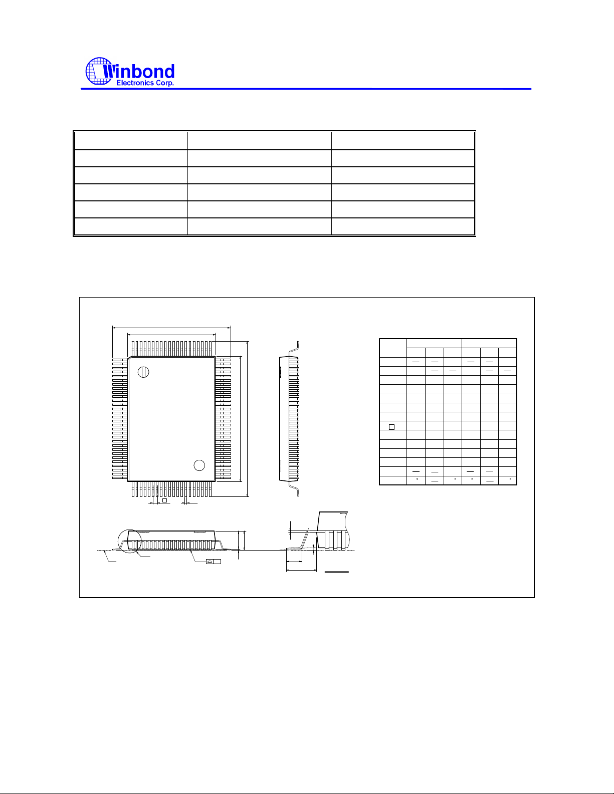
W88111AF/W88112F
ATAPI CD-ROM Decoder & Controller
This specification is subject to change without notice.
Preliminary/Confidential
ORDERING INSTRUCTION
PART NO. PACKAGE FOOTPRINT (=L1X2)
W88111AF PQFP 100 4.8mm
W88111AF-L PQFP 100 3.9mm
W88111AD TQFP 100 2.0mm
W88112F PQFP 100 4.8mm
W88112D TQFP 100 2.0mm
PACKAGE DIMENSIONS
(100-pin QFP, Footprint = 4.8mm, W88111AF/W88112F)
H
D
D
1 80
30
31
Seating Plane
e
See Detail F
81100
E
E H
51
50
b
c
2
A
A
1A
y
θ
L
1
L
Detail F
Dimension in inches Dimension in mm
Symbol
A
0.004
A
1
0.107
A
2
0.010
b
0.004
c
0.546
D
0.782
E
0.020
e
0.728
H
D
0.964
H
E
0.039
L
0.087
L 1
y
θ
Notes:
1. Dimension D & E do not include interlead
flash.
2. Dimension b does not include dambar
protrusion/intrusion.
3. Controlling dimension: Millimeters
4. General appearance spec. should be based
on final visual inspection spec.
Min. Nom. Max. Max.Nom.Min.
0.130
0.10
2.73
0.117
0.112
0.012
0.006 0.15
0.551
0.787
0.026
0.740
0.976
0.047
0.094
0.25
0.016
0.10
0.010
13.87
0.556
19.87
0.792
0.50
0.032
0.752
18.49
0.988
24.49 24.80 25.10
0.055
1.00
0.103
2.21
0.004
0120
2.85
0.30
14.00
20.00
0.65
18.80
1.20
2.40
3.30
2.97
0.40
0.25
14.13
20.13
0.80
19.10
1.40
2.62
0.10
12
Publication Release Date: Aug, 1996
- 62 - Preliminary/ Confidential Revision A0.1
Page 63
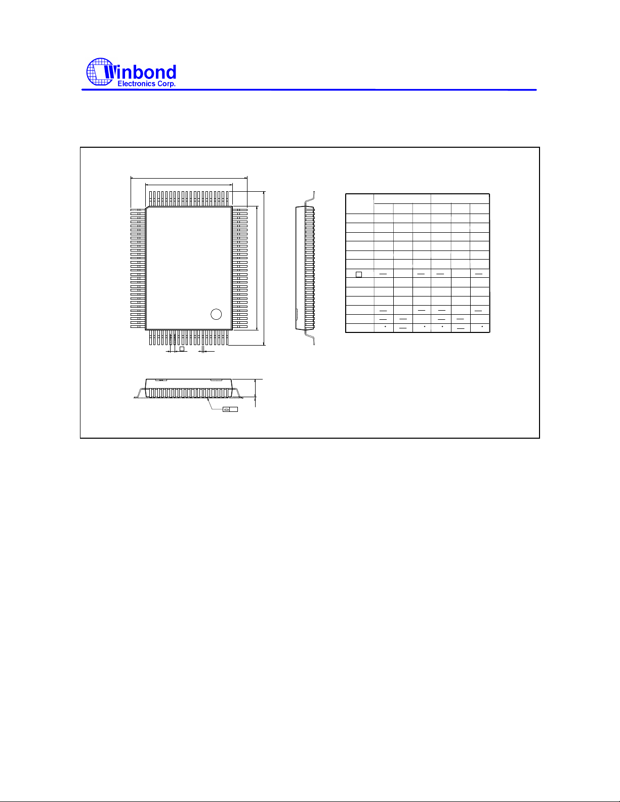
W88111AF/W88112F
ATAPI CD-ROM Decoder & Controller
This specification is subject to change without notice.
(100-pin QFP, Footprint = 3.9mm, W88111AF-L)
H
D
D
E
E H
b
e
2
A
1A
y
Preliminary/Confidential
Dimension in inches Dimension in mm
Symbol
Min. Nom. Max. Max.Nom.Min.
0.002
A
1
A
2
b
c
D
E
e
H
D
H
E
L
L
1
y
θ
0.010 0.020
0.107
0.101
0.008
0.012
0.006 0.15
0.004
0.547
0.551
0.787
0.783
0.026
0.695
0.705
0.931
0.941
0.031
0.025
0.077
0
0.113
0.016
0.008
0.555
0.791
0.715
0.951
0.037
0.003
0.05
0.25 0.50
2.57
0.20
0.10
13.90
19.90
17.65
23.65
0.65
0
7
2.87
2.72
0.40
0.30
0.20
14.00
14.10
20.00
20.10
0.65
18.1517.90
23.90 24.15
0.80
0.95
1.95
0.08
7
Publication Release Date: Aug, 1996
- 63 - Preliminary/ Confidential Revision A0.1
Page 64
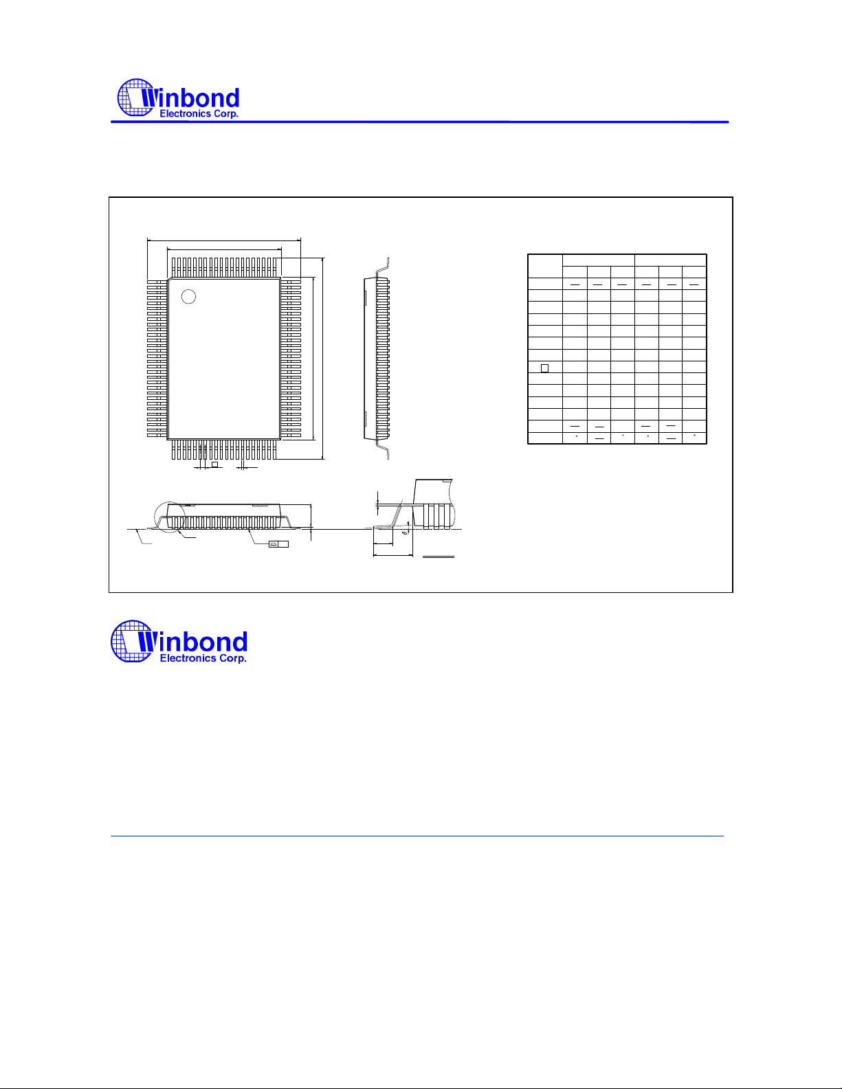
W88111AF/W88112F
ATAPI CD-ROM Decoder & Controller
This specification is subject to change without notice.
(100-pin TQFP, Footprint = 2.0mm, W88111AD/W88112D)
H
D
D
E H
E
Seating Plane
e
See Detail F
b
C
A
2
A
1
y
L
L
1
Preliminary/Confidential
Dimension in inches
Symbol
Min.
Nom.
A
1
A
A
b
c
D
E
e
H
H
L
L
y
0.053
2
0.009
0.004
0.547
0.783
0.020
0.626
D
0.862
E
0.018
1
0.055
0.013
0.006 0.15
0.551
0.787
0.026
0.630
0.866
0.024
0.039
θ
Notes:
1. Dimensions D & E do not include interlead flash.
2. Dimension b does not include dambar
protrusion/intrusion.
3. Controlling dimension: Millimeters
4. General appearance spec. should be based
on final visual inspection spec.
Dimension in mm
Min.
1.35
0.22
0.10
13.90
19.90
0.498
15.90
21.90
0.45
070
Nom.
0.100.050.002 0.004 0.006 0.15
1.40
0.32
14.00
20.00
0.65
16.00
22.00 22.10
0.60
1.00
Max. Max.
0.057
0.015
0.008
0.555
0.791
0.032
0.634
0.870
0.030
0.003
1.45
0.38
0.20
14.10
20.10
0.802
16.10
0.75
0.08
7
Headquarters
No. 4, Creation Rd. III,
Science-Based Industrial Park,
Hsinchu, Taiwan
TEL: 886-3-5770066
FAX: 886-3-5792647
http://www.winbond.com.tw/
Voice & Fax-on-demand: 886-2-7197006
Winbond Electronics (H.K.) Ltd.
Rm. 803, World Trade Square, Tower II,
123 Hoi Bun Rd., Kwun Tong,
Kowloon, Hong Kong
TEL: 852-27513100
FAX: 852-27552064
Taipei Office
11F, No. 115, Sec. 3, Min-Sheng East Rd.,
Taipei, Taiwan
TEL: 886-2-7190505
FAX: 886-2-7197502
Note: All data and specifications are subject to change without notice.
Winbond Electronics North America Corp.
Winbond Memory Lab.
Winbond Microelectronics Corp.
Winbond Systems Lab.
2730 Orchard Parkway, San Jose,
CA 95134, U.S.A.
TEL: 1-408-9436666
FAX: 1-408-9436668
Publication Release Date: Aug, 1996
- 64 - Preliminary/ Confidential Revision A0.1
 Loading...