

Page 1

W83L784R
Winbond H/W
Monitoring IC
Page 2
W83L784R
Preliminary
W83L784R
Data Sheet Revision History
Pages Dates Version Version
on Web
1
2
3
4
5
6
7
8
9
10
n.a. n.a. All the version before 0.50 are for internal use.
n.a. 99/4 0.5 n.a. First publication.
P.55 99/6 0.52 n.a. Schematics updated
P.54 99/6 0.53 n.a. Corrected the length (D) from 10.2mm to 7.2mm
P.56 99/9 0.54 n.a. Updated V0.5 schematics adding pull-high
Main Contents
in the package outline table.
resistors for RESET# (pin15)
Please note that all data and specifications are subject to change without notice. All
the trade marks of products and companies mentioned in this data sheet belong to
their respective owners.
LIFE SUPPORT APPLICATIONS
These products are not designed for use in life support appliances, devices, or
systems where malfunction of these products can reasonably be expected to result
in personal injury. Winbond customers using or selling these products for use in
such applications do so at their own risk and agree to fully indemnify Winbond for
any damages resulting from such improper use or sales.
Confidential, For Beta-site Only Publication Release Date: Sep.
1999
-1 - Revision 0.54
Page 3

W83L784R
Preliminary
TABLE OF CONTENTS
1. GENERAL DESCRIPTION....................................................................................................................5
2. FEATURES..............................................................................................................................................6
2.1 M
2.2 ACTIONS ENABLING................................................................................................................................6
2.3 POWER GOOD .........................................................................................................................................6
2.4 G
2.5 PACKAGE................................................................................................................................................6
3. KEY SPECIFICATIONS ........................................................................................................................7
4. PIN CONFIGURATION.........................................................................................................................7
5. PIN DESCRIPTION................................................................................................................................8
6. FUNCTIONAL DESCRIPTION...........................................................................................................10
6.1 GENERAL DESCRIPTION.........................................................................................................................10
6.2 ACCESS INTERFACE...............................................................................................................................10
6.3 ANALOG INPUTS ...................................................................................................................................15
6.4 T
6.5 FAN SPEED COUNT AND FAN SPEED CONTROL.....................................................................................20
6.6 SMI# ................................................................................................................................................... 24
ONITORING ITEMS
ENERAL
6.2.1 The first serial bus access timing are shown as follow: ................................................................. 10
6.2.2 The serial bus timing of the temperature CPUT1 and CPUT2 is shown as follow: ........................11
6.3.1 Monitor over 4.096V voltage: ......................................................................................................15
6.3.2 Power good for 3V and 5V ...........................................................................................................16
6.3.3 Battery Fault Alarm.....................................................................................................................17
EMPERATURE MEASUREMENT MACHINE
6.4.1 Monitor temperature from thermistor:.......................................................................................... 17
6.4.2 Monitor temperature from Pentium IITM thermal diode or bipolar transistor 2N3904 ...................18
6.4.3 Over Temperature........................................................................................................................18
6.5.1 Fan speed count...........................................................................................................................20
6.5.2 Fan speed control ........................................................................................................................21
6.5.3 Smart Fan Control ....................................................................................................................... 22
6.5.4 Fan Fault Alarm ..........................................................................................................................24
6.6.1 Temperature.................................................................................................................................24
6.6.2 Voltage ........................................................................................................................................26
6.6.3 Fan ..............................................................................................................................................26
...............................................................................................................................................6
................................................................................................................................6
..............................................................................................17
7. REGISTERS AND RAM....................................................................................................................... 27
7.1 C
7.2 INTERRUPT STATUS REGISTER 1 INDEX 41H........................................................................................ 27
ONFIGURATION REGISTER INDEX 40H
Confidential, For Beta-site Only Publication Release Date: Sep.
..............................................................................................27
1999
-2 - Revision 0.54
Page 4
W83L784R
Preliminary
7.3 INTERRUPT STATUS REGISTER 2 INDEX 42H....................................................................................... 28
7.4 SMI MASK REGISTER 1 INDEX 43H...................................................................................................28
7.5 SMIÝ MASK REGISTER 2
7.6 REAL TIME HARDWARE STATUS REGISTER I -- INDEX 45H ......................................................................29
7.7 REAL TIME HARDWARE STATUS REGISTER II -- I NDEX 46H.....................................................................30
7.8 RESERVED REGISTER -- INDEX 47H ........................................................................................................30
7.9 RESERVED REGISTER -- INDEX 48H ........................................................................................................30
7.10 F
AN DIVISOR REGISTER INDEX 49H
7.11 SERIAL BUS ADDRESS (FOR VOLTAGE ,FAN, AND INTERNAL TEMPERATURE ) REGISTER ADDRESS 4AH 31
7.12 CPUT1 TEMPERATURE AND CPUT2 TEMPERATURE SERIAL BUS ADDRESS REGISTER--INDEX 4BH......... 31
7.13 W
INBOND VENDOR
ID (L
7.14 WINBOND VENDOR ID (HIGH BYTE) - INDEX 4DH (NO AUTO INCREASE) ................................................32
7.15 CHIP ID -- INDEX 4EH...........................................................................................................................32
7.16 ACPI T
EMPERATURE INCREMENT REGISTER
7.17 OVT# PROPERTY SELECT - INDEX 50H.................................................................................................. 33
7.18 SMI# PROPERTY SELECT -- INDEX 51H..................................................................................................34
7.19 FANIN1/GPO1, FANIN2/GPO2
7.20 CPUT1/CPUT2 THERMAL SENSOR TYPE REGISTER -- INDEX 53H ..........................................................36
7.21 MISC CONTROL REGISTER -- INDEX 54H ................................................................................................36
7.22 FAN/VBAT F
AULT CONTROL REGISTER
7.23 FAN 1 FAULT HIGH LIMIT COUNT -- INDEX 56H .....................................................................................37
7.24 FAN 2 FAULT LOW LIMIT COUNT -- INDEX 57H ......................................................................................37
AN
7.25 F
AULT HIGH LIMIT COUNT
2 F
7.26 FAN 1 FAULT LOW LIMIT COUNT -- INDEX 59H ......................................................................................38
7.27 VBAT FAULT HIGH LIMIT VALUE -- INDEX 5AH.................................................................................... 38
7.28 VBAT F
AULT LOW LIMIT VALUE
7.29 FAN 1 PRE-SCALE REGISTER-- INDEX 80H ............................................................................................38
7.30 FAN 1 DUTY CYCLE SELECT REGISTER-- 81H (
7.31 FAN 2 PRE-S
CALE REGISTER-- INDEX 82H
7.32 FAN2 DUTY CYCLE SELECT REGISTER-- INDEX 83H..............................................................................40
7.33 FAN CONFIGURATION REGISTER-- INDEX 84H....................................................................................... 40
7.34 CPUT1 T
ARGET TEMPERATURE REGISTER
7.35 CPUT2 TARGET TEMPERATURE REGISTER/ FAN 2 TARGET SPEED REGISTER -- INDEX 86H......................41
7.36 TOLERANCE OF TARGET TEMPERATURE OR TARGET SPEED REGISTER -- INDEX 87H ................................42
7.37 F
AN
1 PWM S
TOP DUTY CYCLE REGISTER
7.38 FAN 2 PWM STOP DUTY CYCLE REGISTER -- 89H (
7.39 FAN 1 START-UP DUTY CYCLE REGISTER -- INDEX 8AH .........................................................................42
AN
7.40 F
TART-UP DUTY CYCLE REGISTER
2 S
7.41 FAN 1 STOP TIME REGISTER -- INDXE 8CH............................................................................................. 43
7.42 FAN 2 STOP TIME REGISTER -- INDEX 8DH.............................................................................................43
7.43 F
AN STEP DOWN TIME REGISTER
7.44 FAN STEP UP TIME REGISTER -- INDEX 8FH............................................................................................44
7.45 TEMPERATURE SENSOR 1 (INTERNAL THERMAL DIODE) OFFSET REGISTER - INDEX 90H ..........................44
7.46 T
EMPERATURE SENSOR
7.47 TEMPERATURE SENSOR 3 (CPU T2) OFFSET REGISTER - INDEX 92H .......................................................45
INDEX 44H ................................................................................................ 29
...................................................................................................30
OW BYTE
NDEX 4CH (AUTO INCREASE
) - I
NDEX 4FH
-- I
AND
BEEP/GPO3 C
-- I
NDEX 58H
-- I
NDEX 5BH
-- I
NDEX 55H
ONTROL REGISTER
............................................................................37
.....................................................................................37
.....................................................................................38
ANK
).........................................................................39
B
0
) ...................................................... 32
.....................................................................32
NDXE 52H
- I
............................34
............................................................................................39
AN
-- I
2 (CPU T1) O
/ F
1 T
NDEX 88H
-- I
NDEX 8BH
-- I
NDEX 8EH
FFSET REGISTER
......................................................................................43
ARGET SPEED REGISTER
.......................................................................42
ANK
)....................................................................42
B
0
..........................................................................43
NDEX 91H
- I
.......................................................44
NDEX 85H
-- I
......................41
Confidential, For Beta-site Only Publication Release Date: Sep.
1999
-3 - Revision 0.54
Page 5

W83L784R
Preliminary
8. VALUE RAM AND LIMIT VALUE .................................................................................................... 46
8.1 VALUE RAM INDEX 20H- 3FH OR 60H - 7FH.....................................................................................46
9. TEMPERATURE SENSOR 2 (CPU T1) REGISTERS........................................................................48
9.1 TEMPERATURE SENSOR 2 TEMPERATURE REGISTER - INDEX 00H ............................................................48
9.2 TEMPERATURE SENSOR 2 CONFIGURATION REGISTER - INDEX 01H .........................................................48
9.3 T
9.4 TEMPERATURE SENSOR 2 OVER-TEMPERATURE REGISTER - INDEX 03H...................................................48
10. TEMPERATURE SENSOR 3 (CPU T2) REGISTERS .................................................................... 49
10.1 TEMPERATURE SENSOR 3 TEMPERATURE REGISTER - INDEX 00H ............................................................49
10.2 TEMPERATURE SENSOR 3 CONFIGURATION REGISTER - INDEX 01H ......................................................... 49
10.3 T
10.4 TEMPERATURE SENSOR 3 OVER-TEMPERATURE REGISTER - INDEX 03H ................................................... 49
11. SPECIFICATIONS............................................................................................................................ 50
11.1 ABSOLUTE MAXIMUM RATINGS.............................................................................................................50
11.2 DC CHARACTERISTICS..........................................................................................................................50
11.3 AC C
EMPERATURE SENSOR
EMPERATURE SENSOR
HARACTERISTICS
11.3.1 Serial Bus Timing Diagram ..........................................................................................................52
YSTERESIS REGISTER
2 H
YSTERESIS REGISTER
3 H
..........................................................................................................................52
NDEX 02H
- I
NDEX 02H
- I
................................................................48
................................................................49
12. HOW TO READ THE TOP MARKING.......................................................................................... 53
13. PACKAGE DRAWING AND DIMENSIONS.................................................................................. 54
14. W83L784R SCHEMATICS...............................................................................................................55
Confidential, For Beta-site Only Publication Release Date: Sep.
1999
-4 - Revision 0.54
Page 6

W83L784R
Preliminary
1. GENERAL DESCRIPTION
W83L784R is an evolving product of W83782D --- Winbond's most popular hardware status
monitoring IC. Specifically designed for the Notebook system, W83L784R can be used to monitor
several critical hardware parameters of the system, including power supply voltages, fan speeds, and
temperatures, which are very important for a high-end Notebook system to work stably and properly.
An 8-bit analog-to-digital converter (ADC) was built inside W83L784R. The W83L784R can
monitor 4 analog voltage inputs, 2 fan tachometer inputs, one on-chip internal temperature sensor
and 2 remote temperature sensors. The remote temperature sensing can be performed by
thermistors, or 2N3904 NPN-type transistors, or directly from IntelTM Deschutes CPU thermal diode
output. The W83L784R provides 2 PWM (pulse width modulation) outputs for the fan speed control
to support the } Thermal Cruise
programmable temperature under the hardware control. Another Fan speed control mode is }Speed
}
Cruise
low active outputs such as fan fault and Battery low which could issue the hardware warning signals
when the fan speed or battery voltage drop out of the preset range. Also the W83L784R provides:
power good reset for 3V and 5V; power down mode for power saving; fault pin for necessary H/W
shutdown control; SMI#, OVT#, GPO# signals for system protection events; I2CTM serial bus interface.
Through the application software or BIOS, the users can read all the monitored parameters of
system from time to time. And a pop-up warning can be also activated when the monitored item was
out of the proper/preset range. The application software could be Winbond's Hardware DoctorTM, or
IntelTM LDCM (LanDesk Client Management), or other management application software. Also the
users can set up the upper and lower limits (alarm thresholds) of these monitored parameters and to
activate one programmable and maskable interrupts. For the spacing saving consideration of the
Notebook system, W83L784R is in the package of 209mil 20pins-SSOP.
to Keep the fan operating in the specific r.p.m.. On the other hand, the W83L784R provides
TM
~ system, which can maintain the CPU or system in the specific
Confidential, For Beta-site Only Publication Release Date: Sep.
1999
-5 - Revision 0.54
Page 7

W83L784R
Preliminary
2. FEATURES
2.1 Monitoring Items
•
2 thermal inputs from remote thermistors or 2N3904 NPN-type transistors or PentiumTM II
(Deschutes) thermal diode output
•
One on-chip temperature detection
•
4 voltage inputs
--- typical for Vcore, +3.3V, +5V, Battery
•
2 sets of fan speed control and fan speed monitoring input
•
WATCHDOG comparison of all monitored values
•
Programmable hysteresis and setting points (alarm thresholds) for all monitored items
2.2 Actions Enabling
• Issue fan fault signal as fans are abnomally stopped
•
Issue battery low signal as bettery voltage is abnomally out of range
•
2 PWM (pulse width modulation) outputs for fan speed control to support } Thermal Cruise
} Speed Cruise
--- Automatically maintain the CPU or system in the specific temperature or keep the fans in the
specific speed under the H/W control
•
Issue SMI#, OVT#, GPO to activate system protection
•
PWR_DN# setting for the Power down mode
•
Warning signal pop-up in application software
TM
~
TM
~ or
2.3 Power Good
•
Issue RESET# outputs as the Power Good signal when 3V and 5V rise across a reset threshold.
2.4 General
•
I2CTM serial bus interface
•
IntelTM LDCM (DMI driver 2.0) support
•
AcerTM ADM (DMI driver 2.0) support
•
Winbond hardware monitoring application software (Hardware Doctor
Windows 95/98
•
Meet WfM 2.0 (Wired for Management) spec.
•
5V Vcc operation
TM
) support, for both
2.5 Package
•
20-pin SSOP (209mil)
Confidential, For Beta-site Only Publication Release Date: Sep.
-6 - Revision 0.54
1999
Page 8
3. KEY SPECIFICATIONS
•
Voltage monitoring accuracy ±1% (Max)
•
Monitoring Temperature Range and Accuracy
- 40°C to +120°C ± 3°C(Max)
•
Supply Voltage 5V
•
Operating Supply Current 2 mA typ.
•
Power Down Suppy Current 10 uA typ.
•
ADC Resolution 8 Bits
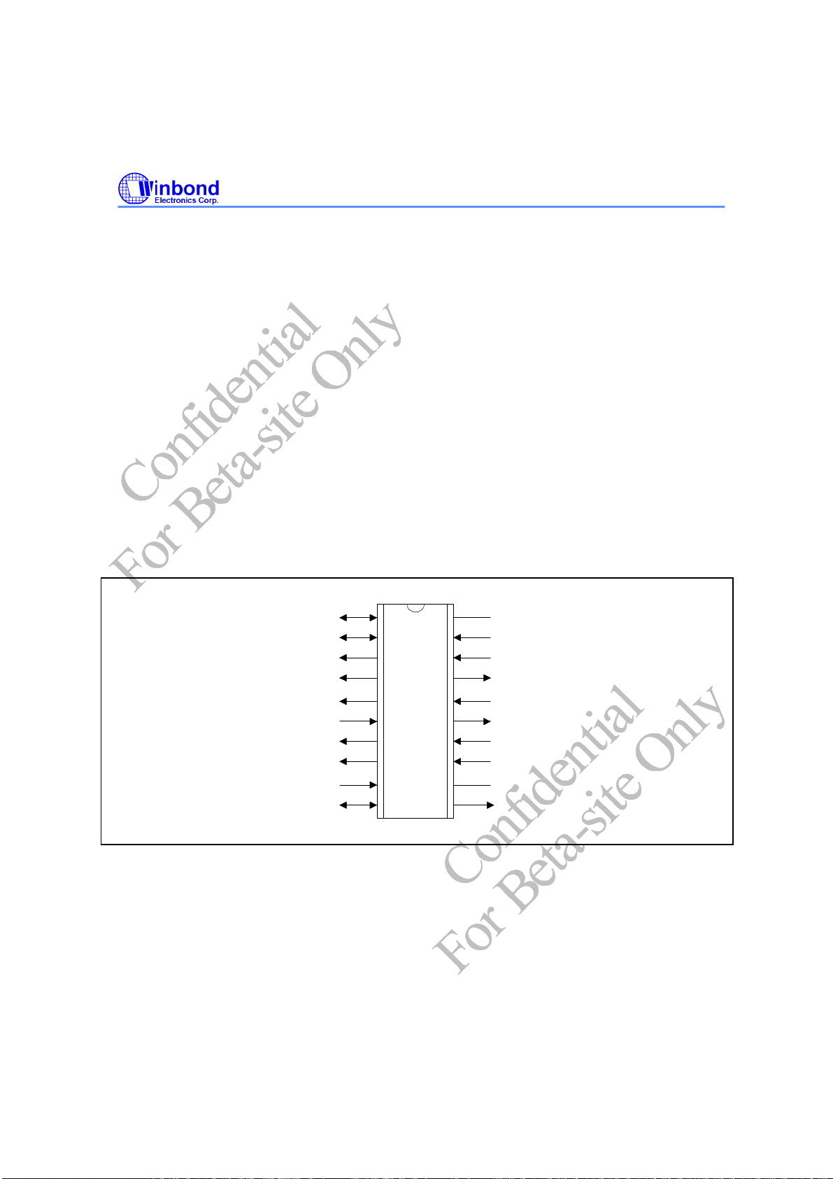
4. PIN CONFIGURATION
W83L784R
Preliminary
FANIN1/GPO1
FANIN2/GPO2
PWMOUT1
PWMOUT2
FANFAULT#/GPO3
PWR_DN#
SMI#
OVT#
SCL
SDA
10
1
2
3
4
5
6
7
8
9
20
19
18
17
16
15
14
13
12
11
VCC
CPUT1/PII1
CPUT2/PII2
VREF
VIN1
RESET#
VIN2(+3.3VIN)
VIN3(VBAT)
GND
BATFAULT#/GPO4
Confidential, For Beta-site Only Publication Release Date: Sep.
-7 - Revision 0.54
1999
Page 9
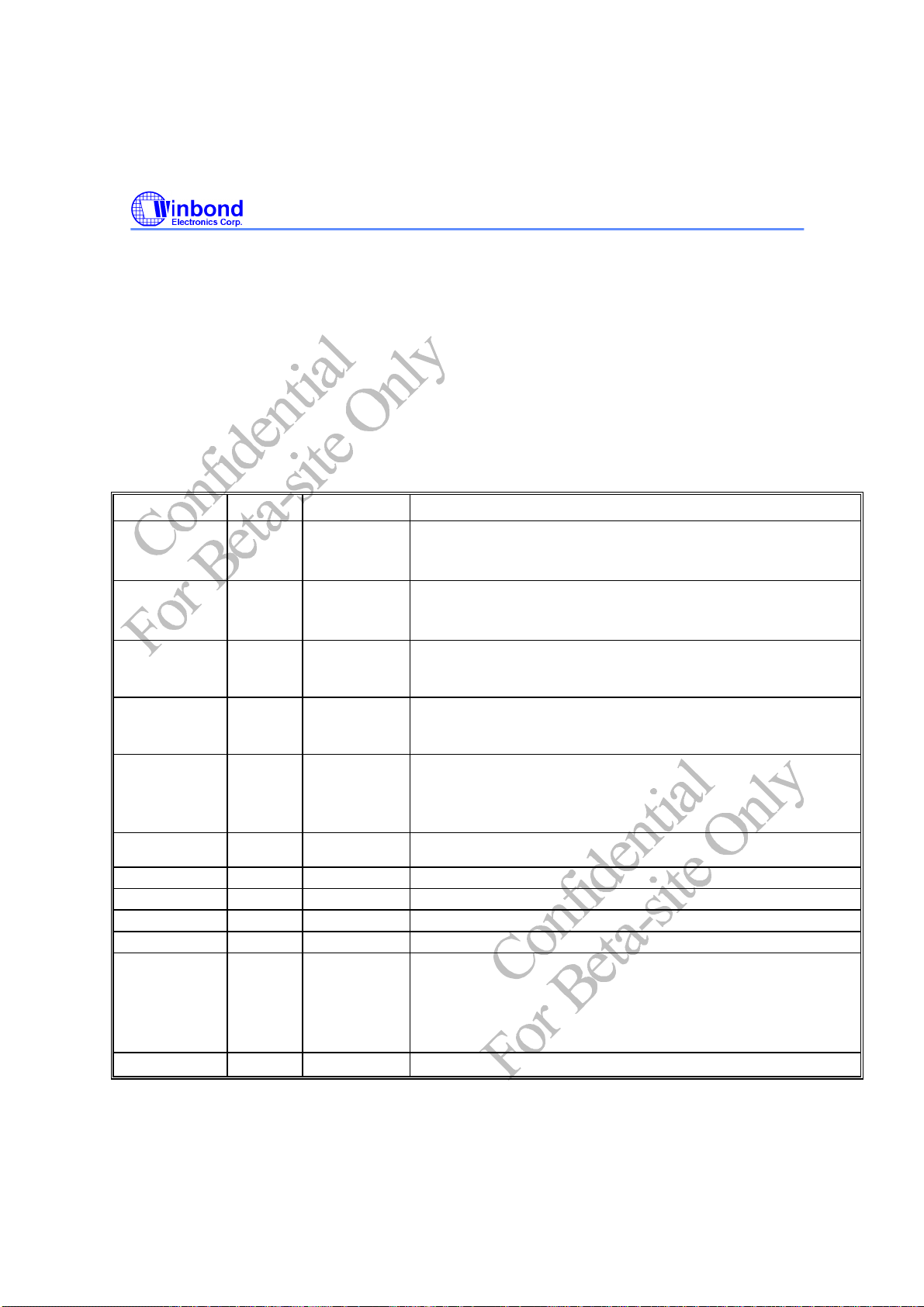
5. PIN DESCRIPTION
I/O
- TTL level bi-directional pin with 12 mA source-sink capability
12t
I/O
- TTL level and schmitt trigger
12ts
OUT12 - Output pin with 12 mA source-sink capability
AOUT - Output pin(Analog)
OD12 - Open-drain output pin with 12 mA sink capability
INt - TTL level input pin
INts - TTL level input pin and schmitt trigger
AIN - Input pin(Analog)
W83L784R
Preliminary
PIN NAME PIN NO.
FANIN1 /
1 INts /
GPO1
TYPE DESCRIPTION
0V to +5V amplitude fan tachometer input. (Default) /
OUT12
General purpose output .
This multi-functional pin is programmable.
FANIN2 /
GPO2
2 INts /
OUT12
0V to +5V amplitude fan tachometer input. (Default) /
General purpose output .
This multi-functional pin is programmable.
PWMOUT1 3 OD
/
12
OUT12
Fan speed control PWM output. This pin is
default
open-drain. It
can be programmed as an output pin which can drive a HIGH or
a LOW.
PWMOUT2 4 OD
/
12
OUT12
Fan speed control PWM output. This pin is
default
open-drain. It
can be programmed as an output pin which can drive a HIGH or
a LOW.
FANFAULT# /
GPO3
5 OD12 Active-Low output. This pin will be a logic LOW when fan1 or
fan2 is abnormally stopped. (Default) /
General purpose output .
This multi-functional pin is programmable.
PWR_DN# 6
INt
Power down input. When set this pin LOW, all output pins would
be tristate except the pin15 RESET# which will keep HIGH.
SMI# 7 OD12 System Management Interrupt.
OVT# 8 OD12 Over temperature Shutdown Output.
SCL 9 INts Serial Bus Clock.
SDA 10 OD12 Serial Bus bi-directional Data.
BATFAULT#
/
GPO4
11 OD12 Active-Low output. This pin will be a logic LOW when Battery
abnormally drops below the low limit or above the high limit.
(Default) /
General purpose output .
This multi-functional pin is programmable.
GND 12 Ground Ground.
Confidential, For Beta-site Only Publication Release Date: Sep.
1999
-8 - Revision 0.54
Page 10
W83L784R
Preliminary
Pin Discription, continued
PIN NAME PIN NO.
VIN3(VBAT) 13 AIN 0V to 4.096V FSR Analog Inputs. ( This pin should be
VIN2(+3.3VIN)
RESET# 15 OUT12 Active-Low reset output. RESET# remains LOW while the
VIN1(VCORE) 16 AIN 0V to 4.096V FSR Analog Inputs.
VREF 17 AOUT Reference Voltage.
CPUT2 /
PII2
CPUT1 /
PII1
VCC 20 POWER +5VCC power supply input.
14 AIN 0V to 4.096V FSR Analog Inputs. (This pin should be
18 AIN Thermistor terminal input.(Default) /
19 AIN Thermistor terminal input.(Default) /
TYPE DESCRIPTION
connected to DC BATTERY. If this voltage is above 4.096V, it
should be reduced with the external resistors so that the input
voltage will be under 4.096V. )
connected to 3VCC .)
5VCC and +3.3V are below the reset threshold. It remains
LOW for 200ms after the reset condition is terminated .
PentiumTM II diode input.
This multi-functional pin is programmable.
PentiumTM II diode input.
This multi-functional pin is programmable.
Confidential, For Beta-site Only Publication Release Date: Sep.
-9 - Revision 0.54
1999
Page 11
W83L784R
Preliminary
6. FUNCTIONAL DESCRIPTION
6.1 General Description
The W83L784R provides at most 4 analog positive inputs, 2 fan speed monitors, 2 sets for
fan PWM (Pulse Width Modulation) Smart Fan Control , 2 remote thermal inputs from remote
thermistors or 2N3904 transistors or Pentium
thermal detection. W83L784R also provides the power good (reset) output for 3V and 5V power
detection and two fault output pins issuing hardware warning if battery and fans become abnormal.
When start the monitor function on the chip, the watch dog machine monitor every function and store
the value to registers. If the monitor value exceeds the limit value, the interrupt status will be set to 1.
6.2 Access Interface
The W83L784R provides I2C Serial Bus to read/write internal reigsters. In the W83L784R
there are three serial bus address. The first address defined at CR[4Ah] can read/write all registers
excluding CPUT1/CPUT2 temperature sensor registers and its address default value is 0101101. The
address for CPUT1 defined at CR[4Bh] bit2-0 only read/write CPUT1 temperature sensor registers
and the address default value is 1001001. The address for CPUT2 defined at CR[4Bh] bit2-0 only
read/write CPUT1 temperature sensor registers and the address default value is 1001000.
TM
II (Deschutes) thermal diode outputs and one on-chip
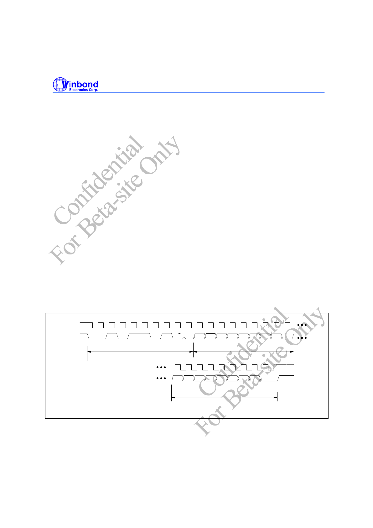
6.2.1 The first serial bus access timing are shown as follow:
(a) Serial bus write to internal address register followed by the data byte
SCL
SDA
0
0 1 0 1 1 0 1 D7 D6 D5 D4 D3 D2 D1 D0
Start By
Master
Figure 1. Serial Bus Write to Internal Address Register followed by the Data Byte
Frame 1
Serial Bus Address Byte
SCL
(Continued)
SDA (Continued)
7 8 0 7 8
R/W
Ack
by
784R
0
D7 D6 D5 D4 D3 D2 D1 D0
Frame 2
Internal Index Register Byte
Frame 3
Data Byte
7 8
784R
Ack
Stop
by
by
Master
Ack
784R
by
Confidential, For Beta-site Only Publication Release Date: Sep.
-10 - Revision 0.54
1999
Page 12
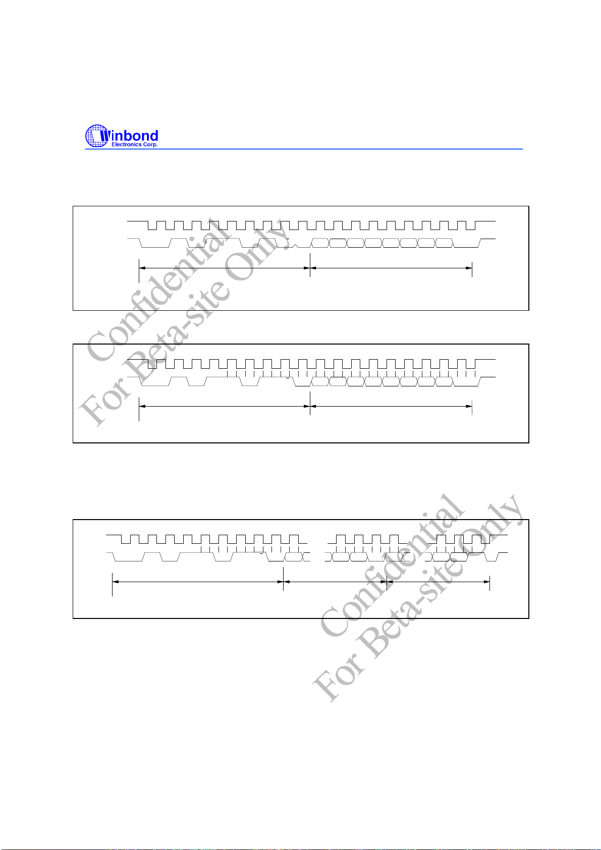
(b) Serial bus write to internal address register only
W83L784R
Preliminary
SCL
SDA
0
0 1 0 1 1 0 1 D7 D6 D5 D4 D3 D2 D1 D0
Start By
Master
Frame 1
Serial Bus Address Byte
Figure 2. Serial Bus Write to Internal Address Register Only
7 8 0 7 8
R/W
Ack
by
784R
0
Frame 2
Internal Index Register Byte
Ack
784R
Stop by
by
Master
(c) Serial bus read from a register with the internal address register prefer to desired location
SCL
SDA
0
0 1 0 1 1 0 1 D7 D6 D5 D4 D3 D2 D1 D0
Start By
Master
Frame 1
Serial Bus Address Byte
Figure 3. Serial Bus Read from Internal Address Register
7 8 0 7 8
R/W
Ack
by
784R
0
Frame 2
Internal Index Register Byte
Ack
Master
Stop by
by
Master
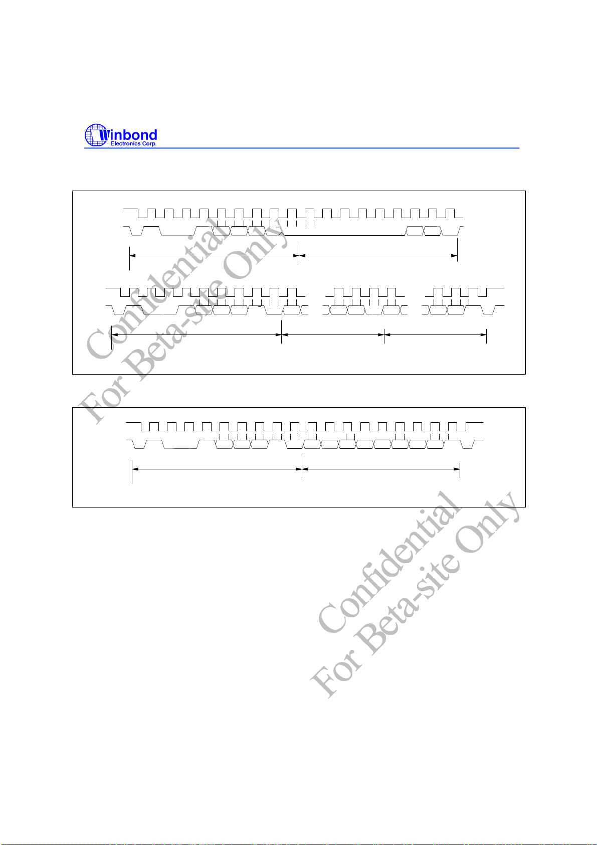
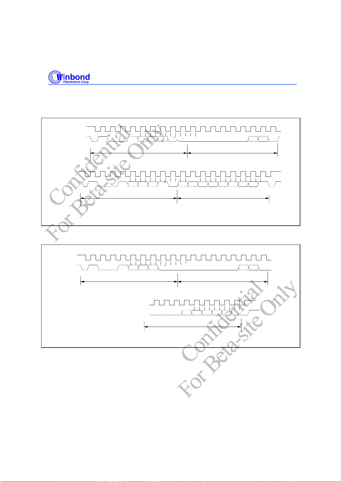
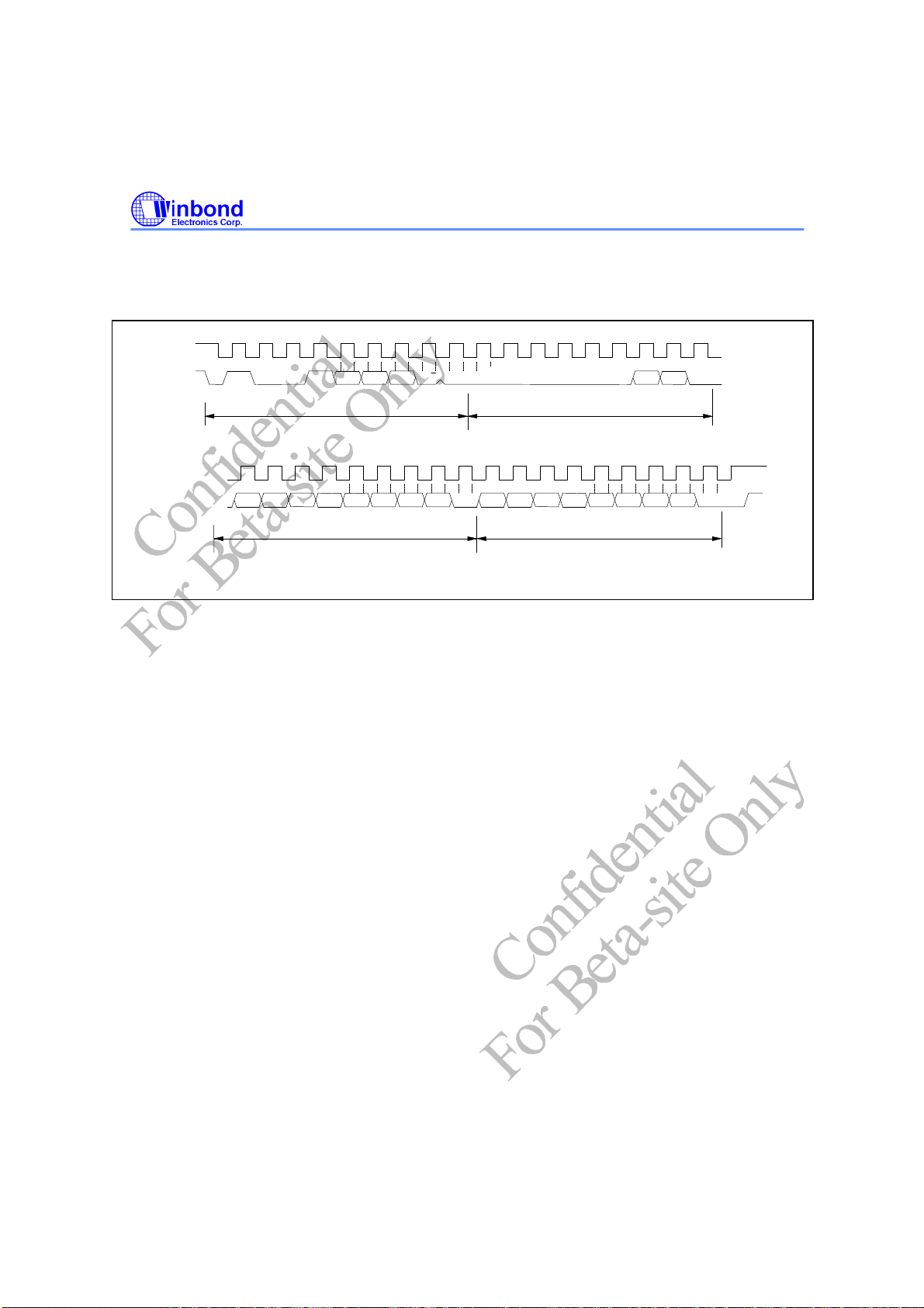
6.2.2 The serial bus timing of the temperature CPUT1 and CPUT2 is shown as follow:
(a) Typical 2-byte read from preset pointer location (Temp, TOS, T
SCL
0
7 8 0 7 8
... ...
)
HYST
0 7
SDA
0 1 0 1 1 0 1 D7 D1 D0
Start By
Master
Frame 1
Serial Bus Address Byte
Figure 4. Typical 2-Byte Read From Preset Pointer Location
R/W
Ack
784R
...
by
Frame 2
MSB Data Byte
D7 D1 D0
...
Master
Ack
by
Frame 3
LSB Data Byte
No Ack
Master
Stop by
Master
by
Confidential, For Beta-site Only Publication Release Date: Sep.
1999
-11 - Revision 0.54
Page 13
W83L784R
Preliminary
(b) Typical pointer set followed by immediate read for 2-byte register (Temp, TOS, T
Frame 2
Pointer Byte
Ack
by
Master
4
D1 D0
0 7
D7 D1 D0
...
Frame 5
LSB Data Byte
Ack
784R
by
SCL
SDA
SCL
SDA
0
1 0 0 1 A2 A1 A0 R/W
Start By
Master
0
Frame 1
Serial Bus Address Byte
7 8 0
0 0 0 0 0 0
Ack
by
784R
7 8 0 7 8
... ...
1 0 0 1 A2 A1 A0 R/W
Start By
Master
Frame 3
Serial Bus Address Byte
0
Figure 5. Typical Pointer Set Followed by Immediate Read for 2-Byte Register
D7 D1 D0
...
Ack
by
784R
Frame 4
MSB Data Byte
(c) Typical read 1-byte from configuration register with preset pointer
SCL
SDA
0
1 0 0 1 A2 A1 A0 R/W D1D5 D4 D3D6
Start By
Master
Frame 1
Serial Bus Address Byte
7 8 0
D7 D2
Ack
by
782D
Frame 2
Data Byte
8
7
D0
No Ack
by
Master
HYST
No Ack
by
Master
Stop by
Master
)
Stop by
Master
Figure 6. Typical 1-Byte Read From Configuration With Preset Pointer
Confidential, For Beta-site Only Publication Release Date: Sep.
1999
-12 - Revision 0.54
Page 14
W83L784R
(d) Typical pointer set followed by immediate read from configuration register
Preliminary
0
1 0 0 1 A2 A1 A0 R/W
Start By
Master
0
1 0 0 1 A2 A1 A0 R/W
Serial Bus Address Byte
Frame 1
Serial Bus Address Byte
Frame 3
SCL (Cont..)
SDA (Cont..)
Repea
Start
Master
SCL
SDA
By
Figure 7. Typical Pointor Set Followed by Immediate Read from Temp 2/3 Configuration Register
(e) Temperature configuration register Write
SCL
SDA
0
1 0 0 1 A2 A1 A0 R/W
Start By
Master
Frame 1
Serial Bus Address Byte
7 8 0
0 0 0 0 00
Ack
by
784R
7 8 0
D7 D5 D4
D6 D3
Ack
by
784R
7 8 0
0 0 0 0 0 0 0
Ack
by
784R
Frame 4
MSB Data Byte
Pointer Byte
Frame 2
Frame 2
Pointer Byte
4
4
D2 D1 D0
D1 D0
D1 D0
7
No Ack
Master
7 8
7 8
8
by
Ack
by
784R
Ack
784R
...
...
by
Stop by
Master
SCL (Cont...)
SDA (Cont...)
0
0 0 D4 D3 D2 D10 D0
Configuration Data Byte
Figure 8. Configuration Register Write
Frame 3
7 8
Ack
784R
Stop
by
by
Master
Confidential, For Beta-site Only Publication Release Date: Sep.
1999
-13 - Revision 0.54
Page 15
(f) Temperature TOS and T
SCL
SDA
0
1 0 0 1 A2 A1 A0 R/W
Start By
Master
Serial Bus Address Byte
HYST
Frame 1
write
7 8 0
Ack
by
784R
W83L784R
Preliminary
4
0
0
0 0 0 0
Frame 2
Pointer Byte
D1 D0
7 8
Ack
by
784R
SCL (Cont...)
SDA (Cont...)
0
D6 D5 D4 D3 D2 D1D7 D0
Frame 3
MSB Data Byte
Figure 9. Configuration Register Write
7 8
0 7 8
D6 D5 D4 D3 D2 D1D7 D0
Ack
by
784R
Frame 4
LSB Data Byte
Ack
Stop
by
by
784R
Master
Confidential, For Beta-site Only Publication Release Date: Sep.
1999
-14 - Revision 0.54
Page 16
W83L784R
CPUT1
Preliminary
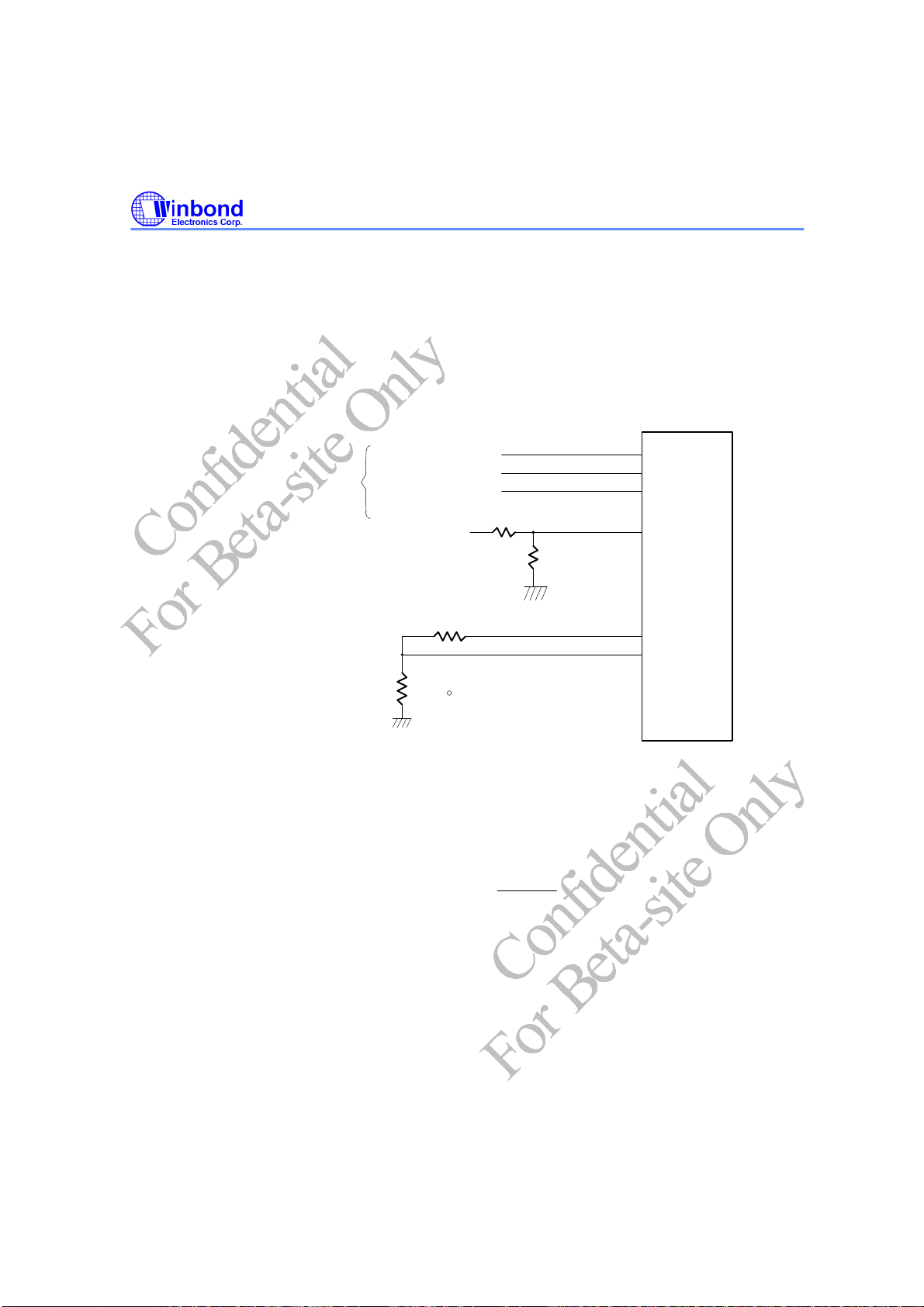
6.3 Analog Inputs
The maximum input voltage of the analog pin is 4.096V because the 8-bit ADC has a 16mv LSB.
Really, the application of the PC monitoring would most often be connected to power suppliers. The
CPU V-core voltage and +3.3V voltage can directly connected to these analog inputs. The 5VSB and
battery inputs should be reduced a factor with external resistors so as to obtain the input range. As
Figure 10 shows.
Positive Inputs
Typical Thermister
Connection
**The connections of CPUT2
is same as CPUT1
VIN1(VCORE)
VIN2(+3.3V)
10V(Battery DC)
R
10K, 1%
R
THM
10K, 25 C
VCC
232K, 1%
R1
VIN3(VBAT)
VREF
R2
99K, 1%
Pin 16
Pin 14
Pin 20
Pin 13
Pin 17
Pin 19
8-bit ADC
with
16mV LSB
Figure. 10.
6.3.1 Monitor over 4.096V voltage:
The input voltage VIN3 can be expressed as following equation.
R
VIN V
3
= ×
BAT DC
−
2
R R
+
1 2
The value of R1 and R2 can be selected to 232K Ohms and 99K Ohms, respectively, when the input
voltage V
is 10V. The node voltage of VIN3 can be subject to less than 4.096V for the maximun
BAT-DC
input range of the 8-bit ADC. The pin 24 is connected to the power supply VCC with +5V. There are
two functions in this pin with 5V. The first function is to supply internal analog power in the W83L784R
and the second function is that this voltage with 5V is connected to internal serial resistors to monitor
the +5V voltage. The value of two serial resistors are 34K ohms and 50K ohms so that input voltage
to ADC is 2.98V which is less than 4.096V of ADC maximum input voltage. The express equation can
represent as follows.
Confidential, For Beta-site Only Publication Release Date: Sep.
1999
-15 - Revision 0.54
Page 17
W83L784R
Preliminary
K
50
V VCC
= ×
in
50 34
where VCC is set to 5V.
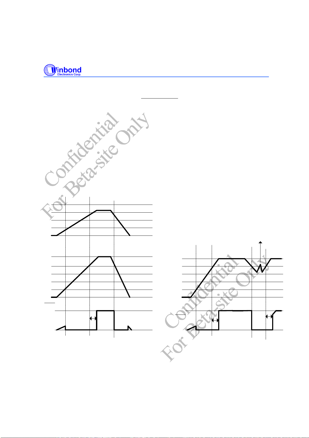
6.3.2 Power good for 3V and 5V
On power up, once VCC(5V) reaches 1V, RESET# will be a logic low. As 3V and VCC(5V)
rise, RESET# remains asserted. If 3V and VCC(5V) both exceed the reset threshold, RESET
becomes a logic high after a time equal to the reset pulse width (tRST, typically 200ms).(Figure 11).
If a power fail or a brownout happens(i.e. 3V or VCC(5V) drops below the threshold), RESET# output
is asserted. As long as the 3V and VCC(5V) remain below the reset threshold, RESET# output
remains asserted. Therefore, a brownout condition that interrupts a previously initiated reset pulse
causes an additional 200ms delay from the time the latest interruption occurred. On power-on, once
3Vor VCC(5V) drops below the reset threshold, RESET# are guaranteed to be asserted for VCC ≥ 1V.
3.3V
4
3
2
1
0
V
RST
V
RST
Ω
K K
+
Ω Ω
≅
2 98
.
V
The time of voltage over 4V
is less than tRST
VCC
5
4
3
2
1
0
RESET
V
RST
5
tRST
0
V
RST
VCC
5
4
3
2
1
0
5
RESET
0
tRST
V
RS
V
RS
Figure 11
Confidential, For Beta-site Only Publication Release Date: Sep.
1999
-16 - Revision 0.54
V
RS
tRST
Page 18
W83L784R
Preliminary
6.3.3 Battery Fault Alarm
W83L784R provides a good protection for DC battery. Set VIN3 to monitor DC battery
voltage and enable VBAT fault function. When VIN3(pin13) voltage exceeds high or low limit value,
pin BATFAULT# will be asserted.
6.4 Temperature Measurement Machine
The temperature data format is 8-bit two?-complement for internal sensor and 9-bit two -complement
for sensor CPUT1 and CPUT2. The 8-bit temperature data can be obtained by reading the CR[27h].
The 9-bit temperature data (CPUT1 and CPUT2) can be obtained by reading CR[00h] of its serial bus
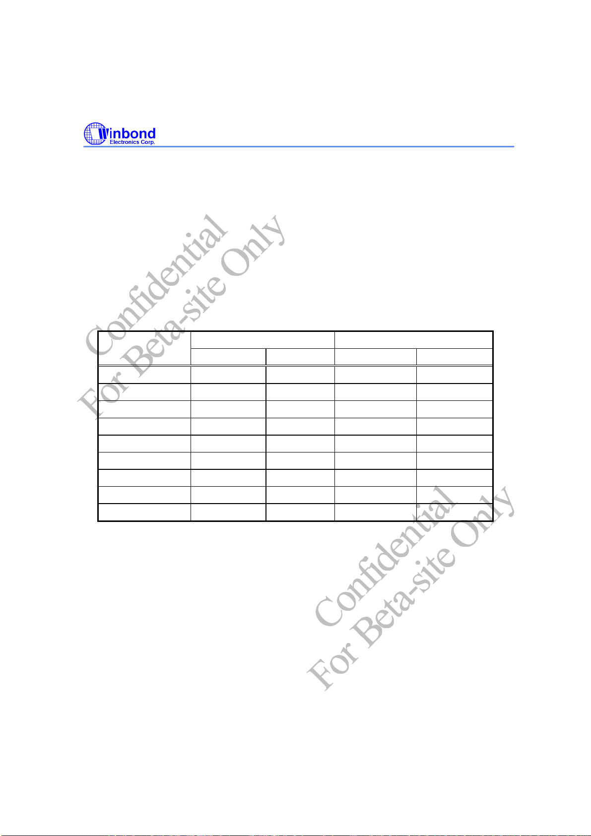
address. The format of the temperature data is show in Table 1.
Temperature 8-Bit Digital Output 9-Bit Digital Output
8-Bit Binary
6.4.1 Monitor temperature from thermistor:
The W83L784R can connect three thermistors to measure three different envirment temperature. The
specification of thermistor should be considered to (1) β value is 3435K, (2) resistor value is 10K
ohms at 25°C. In the Figure 10, the themistor is connected by a serial resistor with 10K Ohms, then
connect to VREF (pin 17).
+125°C 0111,1101 7Dh 0,1111,1010 0FAh
+25°C 0001,1001 19h 0,0011,0010 032h
+1°C 0000,0001 01h 0,0000,0010 002h
+0.5°C - - 0,0000,0001 001h
+0°C 0000,0000 00h 0,0000,0000 000h
-0.5°C - - 1,1111,1111 1FFh
-1°C 1111,1111 FFh 1,1111,1110 1FFh
-25°C 1110,0111 E7h 1,1100,1110 1CEh
-55°C 1100,1001 C9h 1,1001,0010 192h
8-Bit Hex 9-Bit Binary 9-Bit Hex
Table 1.
Confidential, For Beta-site Only Publication Release Date: Sep.
1999
-17 - Revision 0.54
Page 19
W83L784R
Preliminary
6.4.2 Monitor temperature from Pentium IITM thermal diode or bipolar transistor 2N3904
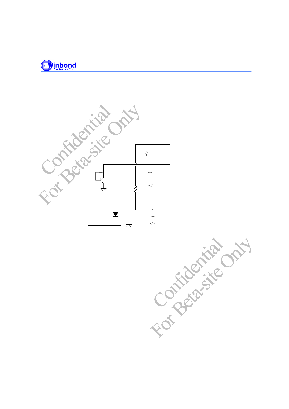
The W83L784R can alternate the thermistor to Pentium IITM (Deschutes) thermal diode interface or
transistor 2N3904 and the circuit connection is shown as Figure 12. The pin of Pentium IITM D- is
connected to power supply ground (GND) and the pin D+ is connected to pin PIIx in the W83L784R.
The resistor R=30K ohms should be connected to VREF to supply the diode bias current and the
bypass capacitor C=3300pF should be added to filter the high frequency noise. The transistor 2N3904
should be connected to a form with a diode, that is, the Base (B) and Collector (C) in the 2N3904
should be tied togeter to act as a thermal diode.
VREF
Bipolar Transistor
Temperature Sensor
C
B
2N3904
E
OR
Pentium II
CPU D+
Therminal
Diode
D-
R=30K, 1%
PIITDx
C=3300pF
W83L784R
R=30K, 1%
PIITDx
C=3300pF
Figure 12.
6.4.3 Over Temperature
W83L784R provides two external thermal sensors to detect temperature. When detected
temperature exceeds the over-temperature value, pin OVT# will be asserted until the
temperature goes below the hysteresis temperature. Pin OVT# has 3 operating modes:
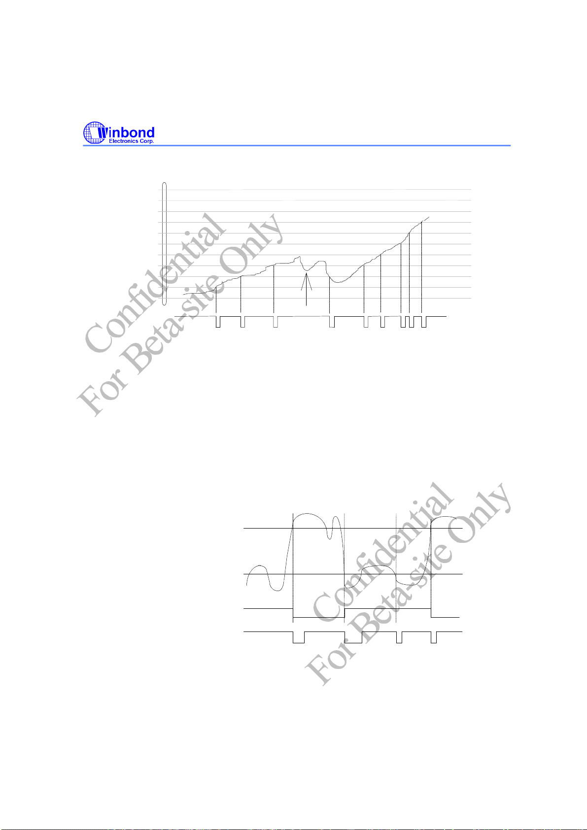
6.4.3.1 ACPI Mode :
At this mode, temperature exceeding one level of temperature sepeartion , starting from 0
degree, causes the OVT# output activated. OVT# will be activated again once temperature
exceeding the next level. OVT# output will act the same manner when temperature goes down.
(Figure 13). The granularity of temperature separation between each OVT# output signal can be
programmed at Bank0 CR[4Fh].
The piority of this mode is higher than Comparator mode and Interrupt mode .
Confidential, For Beta-site Only Publication Release Date: Sep.
-18 - Revision 0.54
1999
Page 20
('C)
100
90
80
70
60
5
40
30
20
10
W83L784R
Preliminary
Current Temperature
0
OVT#
Figure 13.
6.4.3.2 Comparator Mode :
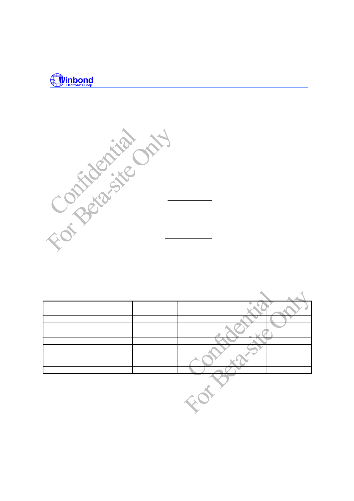
At this mode, temperature exceeding TO causes the OVT# output activated until the temperature
is less than T
. ( Figure 14)
HYST
6.4.3.3 Interrupt Mode:
At this mode, temperature exceeding TO causes the OVT# output activated indefinitely until reset
by reading CPUT1 or CPUT2 registers. Temperature exceeding TO , then OVT# asserted, and
then temperature going below T
will also cause the OVT# activated indefinitely until reset by
HYST
reading temperature sensor2 or sensor 3 registers. Once the OVT# is activated by exceeding TO
, then reset, if the temperature remains above T
, the OVT# will not be activated again.(
HYST
Figure 14)
To
T
HYST
(Comparator Mode; default)
OVT#
(Interrupt Mode)
OVT#
* * *
*
*Interrupt Reset when CPUT1/CPUT2 is read
Figure 14.
Confidential, For Beta-site Only Publication Release Date: Sep.
1999
-19 - Revision 0.54
Page 21
W83L784R
Preliminary
6.5 FAN Speed Count and FAN Speed Control
6.5.1 Fan speed count
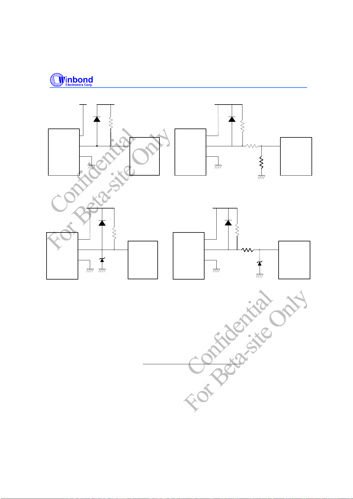
Inputs are provides for signals from fans equipped with tachometer outputs. The level of these signals
should be set to TTL level, and maximum input voltage can not be over +5.5V. If the input signals
from the tachometer outputs are over the VCC, the external trimming circuit should be added to
reduce the voltage to obtain the input specification. The normal circuit and trimming circuits are
shown as Figure 15.
Determine the fan counter according to:
6
×
1 35 10
Count
In other words, the fan speed counter has been read from register CR28 or CR29 or CR2A, the fan
speed can be evaluated by the following equation.
RPM
=
The default divisor is 2 and defined at CR49.bit0~2, bit4~6 which are three bits for divisor. That
provides very low speed fan counter such as power supply fan. The followed table is an example for
the relation of divisor, PRM, and count.
Divisor Nominal
PRM
1 8800 6.82 ms
2 (default)
128 68 872.64 ms
4 2200 27.27 ms
8 1100 54.54 ms
16 550 109.08 ms
32 275 218.16 ms
64 137 436.32 ms
4400 13.64 ms
Time per
Revolution
.
=
RPM Divisor
×
×
1 35 10
.
Count Divisor
Table 2.
×
Counts 70% RPM Time for 70%
153
153
153
153
153
153
153
153
6
6160 9.74 ms
3080 19.48 ms
1540 38.96 ms
770 77.92 ms
385 155.84 ms
192 311.68 ms
96 623.36 ms
48 1246.72 ms
Confidential, For Beta-site Only Publication Release Date: Sep.
1999
-20 - Revision 0.54
Page 22
+5V
+5V
W83L784R
Preliminary
+5V
diode diode
+5V
FAN Out
GND
FAN
Connector
Figure 15-1. Fan with Tach Pull-Up to +5V
+5V
diode
+5V
FAN
Connector
FAN Out
GND
Fan Input
3.9V Zener
Fan Input
Pull-up resister
Pull-up resister
4.7K Ohms
Pin 1 / 2
W83L784
> 1K
Pin 1 / 2
W83L784
Pull-up resister
4.7K Ohms
+5V
FAN Out
GND
FAN
Connector
Figure 15-2. Fan with Tach Pull-Up to +5V, or Totem-Pole
+5V
FAN Out
GND
FAN
Connector
Output and Register Attenuator
+5V
diode
2K
Pull-up resister < 1K
or totem-pole output
> 1K
3.9V Zener
Fan Input
10K
Fan Input
Pin 1 / 2
W83L784R
Pin 1 / 2
W83L784R
Figure 15-3. Fan with Tach Pull-Up to +5V
and Zener Clamp
Figure 15-4. Fan with Tach Pull-Up to +5V, or
Totem-Pole Putput and Zener Clamp
6.5.2 Fan speed control
The W83L784R provides four sets for fan PWM speed control. The duty cycle of PWM can be
programmed by a 8-bit register which are defined in the Bank0 CR81h and CR83h. The default duty
cycle is set to 100%, that is, the default 8-bit registers is set to FFh. The expression of duty can be
represented as follows.
Programmed 8 - bit Register Value
Duty cycle
− = ×(%) 100%
255
Confidential, For Beta-site Only Publication Release Date: Sep.
1999
-21 - Revision 0.54
Page 23

W83L784R
Preliminary
+5V
R1
R2
D
G
PWM Clock Input
NMOS
S
Figure 16.
6.5.3 Smart Fan Control
Smart Fan Control provides two mechanisms. One is Thermal Cruise mode and the other is
Fan Speed Cruise mode.
6.5.3.1 Thermal Cruise mode
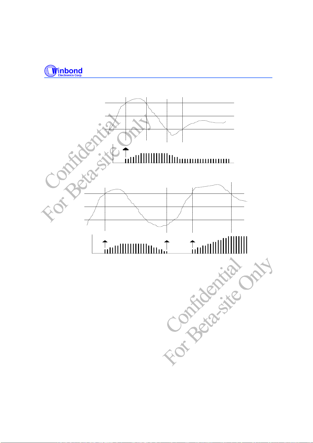
At this mode, W83L784R provides the Smart Fan system which can control the fan speed
automatically depend on current temperature to keep it with in a specific range. At first a wanted
temperature and interval must be set (ex. 55 °C ± 3 °C) by BIOS, as long as the real temperature
remains below the setting value, the fan will be off. Once the temperature exceeds the setting high
limit temperature ( 58°C), the fan will be turned on with a specific speed set by BIOS (ex: 80% duty
cycle) and automatically controlled its PWM duty cycle with the temperature varying. Three
conditions may occur :
(1) If the temperature still exceeds the high limit (ex: 58°C), PWM duty cycle will increase slowly. If
the fan has been operating in its fully speed but the temperature still exceeds the high limit(ex: 58°C),
a warning message or a fan_fault signal(pin5) will be issued to protect the system.
(2) If the temperature goes below the high limit (ex: 58°C), but above the low limit (ex: 52°C), the fan
speed will be fixed at the current speed because the temperature is in the target area(ex: 52 °C ~
58°C).
(3) If the temperature goes below the low limit (ex: 52°C), PWM duty cycle will decrease slowly to 0
until the temperature exceeds the low limit.
Figure 17 gives an illustration for Thermal Cruise Mode .
+
-
PNP Transistor
C
FAN
Confidential, For Beta-site Only Publication Release Date: Sep.
1999
-22 - Revision 0.54
Page 24
58`C
55`C
58`C
55`C
52`C
PWM
Duty
Cycle
100
50
A B
Fan Start = 20%
0
D
C
Figure 17-1.
A B C
W83L784R
Preliminary
D
52`C
PWM
Duty
Cycle
100
Fan Start = 20% Fan Stop = 10%
50
0
Fan Start = 20%
Figure 17-2.
6.5.3.2 Fan Speed Cruise mode
At this mode, W83L784R provides the Smart Fan system which can control the fan speed
automatically depend on current fan spesed to keep it with in a specific range. A wanted fan speed
count and interval must be set (ex. 160 ± 10 ) by BIOS. As long as the fan speed count is the specific
range, PWM duty will keep the current value. If current fan speed count is higher than the high limit
(ex. 160+10), PWM duty will be increased to keep the count less than the high limit. Otherwise, if
current fan speed is less than the low limit(ex. 160-10), PWM duty will be decreased to keep the
count higher than the low limit. See Figure 18 example.
Confidential, For Beta-site Only Publication Release Date: Sep.
1999
-23 - Revision 0.54
Page 25

W83L784R
Preliminary
Count
PWM
Duty
Cycle
170
160
150
100
50
A
0
Figure 18.
Of cource, Smart Fan control system can be disabled and the fan speed control algorithem can be
progrmmed by BIOS or application software.
6.5.4 Fan Fault Alarm
C
W83L784R can monitor fan speed by detecting fan speed counter value. When fan speed
count is higher than high limit count value(CR58h) or is less than low limit count value(CR59h), pin
FANFAULT# is asserted.
6.6 SMI#
6.6.1 Temperature
Pin SMI# for temperature has 3 modes.
6.6.1.1 Comparator Interrupt Mode
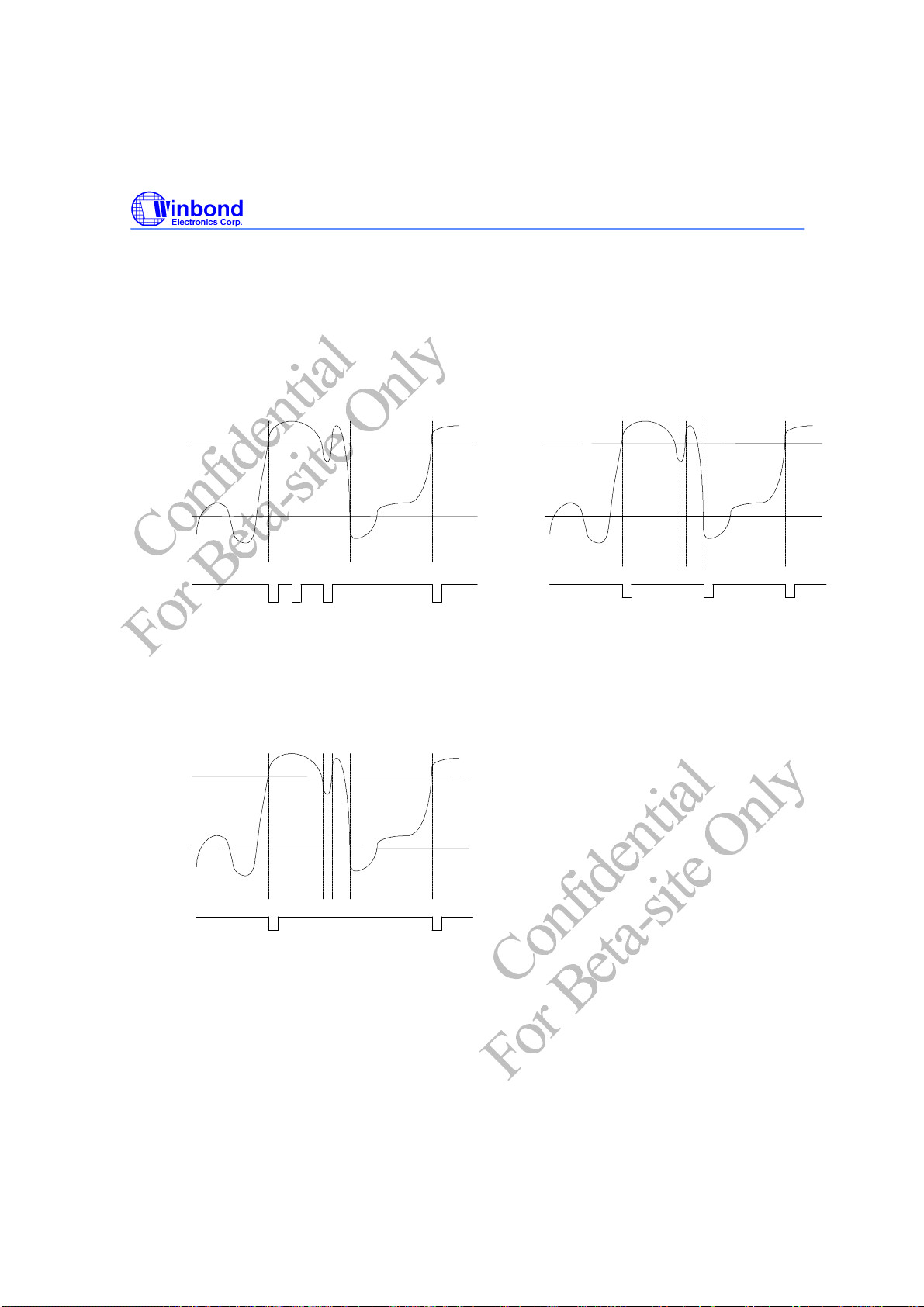
Temperature exceeding TO causes an interrupt and this interrupt will be reset by reading all the
Interrupt Status Registers. Once an interrupt event has occurred by exceeding TO, then reset, if
the temperature remains above the T
has completed. If an interrupt event has occurred by exceeding TO and not reset, the interrupts
will not occur again. The interrupts will continue to occur in this manner until the temperature
goes below T
. ( Figure 19-1 )
HYST
6.6.1.2 Two-Times Interrupt Mode
Temperature exceeding TO causes an interrupt and then temperature going below T
cause an interrupt if the previous interrupt has been reset by reading all the interrupt Status
Register. Once an interrupt event has occurred by exceeding TO , then reset, if the temperature
remains above the T
, the interrupt will not occur. (Figure 19-2 )
HYST
, the interrupt will occur again when the next conversion
HYST
HYST
will also
Confidential, For Beta-site Only Publication Release Date: Sep.
1999
-24 - Revision 0.54
Page 26
6.6.1.3 One-Time Interrupt Mode
W83L784R
Preliminary
Temperature exceeding TO causes an interrupt and then temperature going below T
HYST
cause an interrupt. Once an interrupt event has occurred by exceeding TO , then going below
T
an interrupt will not occur again until the temperature exceeding TO. (Figure 19-3 )
HYST,
T
OI
T
HYST
SMI# SMI#
Figure 19-1. Comparator Interrupt Mode
* * *
* * * **
*Interrupt Reset when Interrupt Status Registers are read
T
T
OI
HYST
Figure 19-2. Two-Times Interrupt Mode
will not
T
OI
T
HYST
SMI#
*Interrupt Reset when Interrupt Status Registers are read
Figure 19-3. One-Time Interrupt Mode
* *
Confidential, For Beta-site Only Publication Release Date: Sep.
-25 - Revision 0.54
1999
Page 27
W83L784R
Preliminary
6.6.2 Voltage
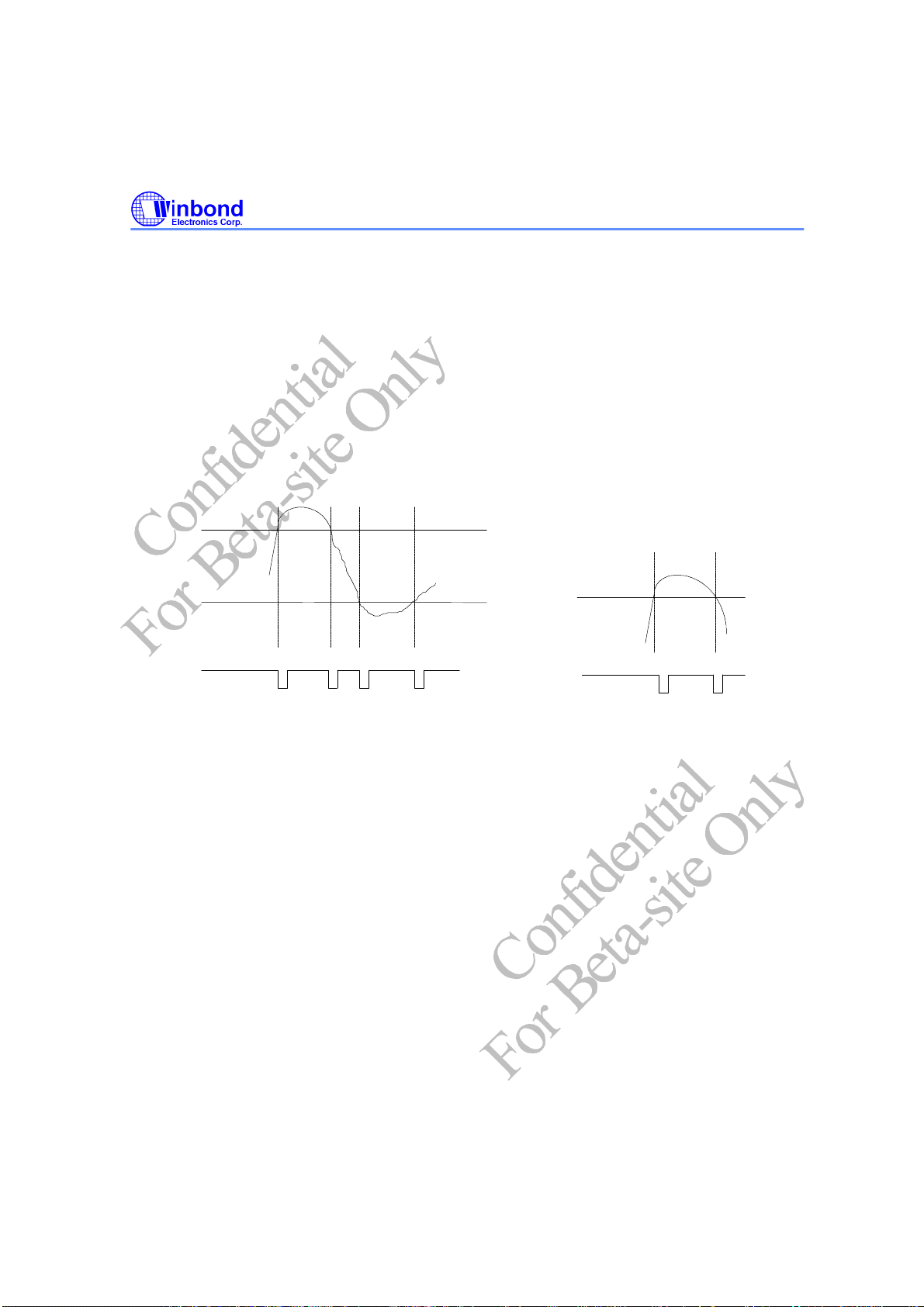
SMI# interrupt for voltage is Two-Times Interrupt Mode. Voltage exceeding high limit or going
below low limit will causes an interrupt if the previous interrupt has been reset by reading all the
interrupt Status Register. (Figure 20-1 )
6.6.3 Fan
SMI# interrupt for fan is Two-Times Interrupt Mode. Fan count exceeding the limit, or exceeding
and then going below the limit( set at value ram index 3Bh and 3Ch) , will causes an interrupt if
the previous interrupt has been reset by reading all the interrupt Status Register. (Figure 20-2 )
High limit
Low limit
SMI#
Figure 20-1. Voltage SMI# Mode
* * *
Fan Count limit
*
*Interrupt Reset when Interrupt Status Registers are read
SMI#
Figure 20-2. Fan SMI# Mode
*
*
Confidential, For Beta-site Only Publication Release Date: Sep.
1999
-26 - Revision 0.54
Page 28
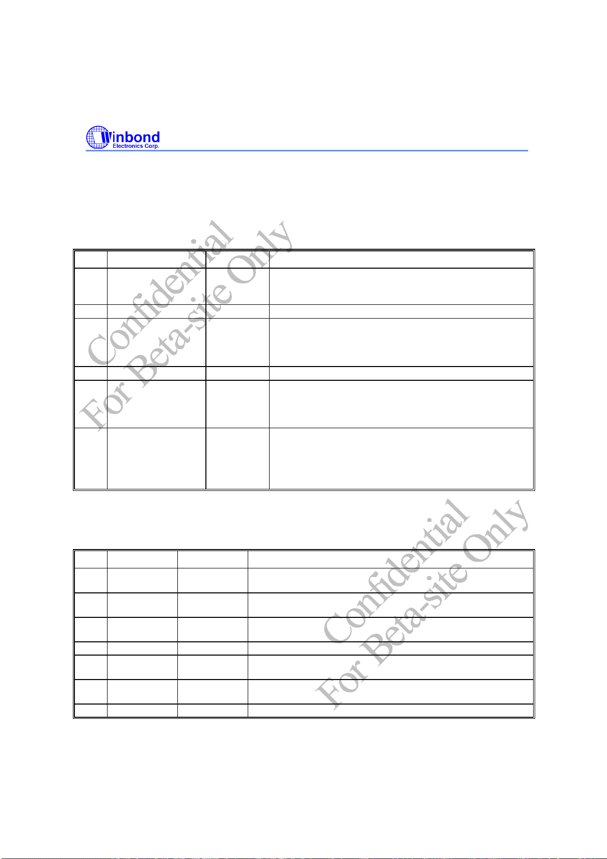
7. REGISTERS AND RAM
7.1 Configuration Register ¾ Index 40h
Power on default [7:0] = 0000,0001 b
W83L784R
Preliminary
Bit Name Read/Write
7 INITIALIZATION Read/Write A one restores power on default value to all registers
6-4 Reserved Read/Write Reserved
3 DIS_PWROK Read/Write Disable Power OK Function
2 Reserved Reserved Reserved
1 INT_ Clear Read/Write A one disables the SMI# and IRQ# outputs without
0 Start Read/Write A one enables startup of monitoring operations, a zero
7.2 Interrupt Status Register 1¾ Index 41h
Power on default [7:0] = 0000,0000 b
Description
except the Serial Bus Address register. This bit clears
itself since the power on default is zero.
. If this bit set to 1, the
PWR_DN# (Pin 6) will keep logical high no mater what
the pwoer VDD or +3.3V drop to the threshold voltage
(4.0v and 2.6v, respectively).
affecting the contents of Interrupt Status Registers. The
device will stop monitoring. It will resume upon clearing
of this bit.
puts the part in standby mode.
Note:
The outputs of Interrupt pins will not be cleared if
the user writes a zero to this location after an interrupt
has occurred unlike "INT_Clear'' bit.
Bit Name Read/Write Description
7 TEMP3 Read Only A one indicates a High or Low limit has been exceeded from
CPUT2 sensor.
6 TEMP2 Read Only A one indicates a High or Low limit has been exceeded from
CPUT1 sensor.
5 TEMP1 Read Only A one indicates a High or Low limit has been exceeded from
W83L784R internal temperature sensor.
4 Reserved Reserved Reserved
3 VCCIN Read Only A one indicates a High or Low limit has been exceeded. (
VCC, +5V)
2 3VIN Read Only A one indicates a High or Low limit has been exceeded.
(VIN2)
1 VBATIN Read Only A one indicates a High or Low limit has been exceeded.(VIN3
Confidential, For Beta-site Only Publication Release Date: Sep.
1999
-27 - Revision 0.54
Page 29
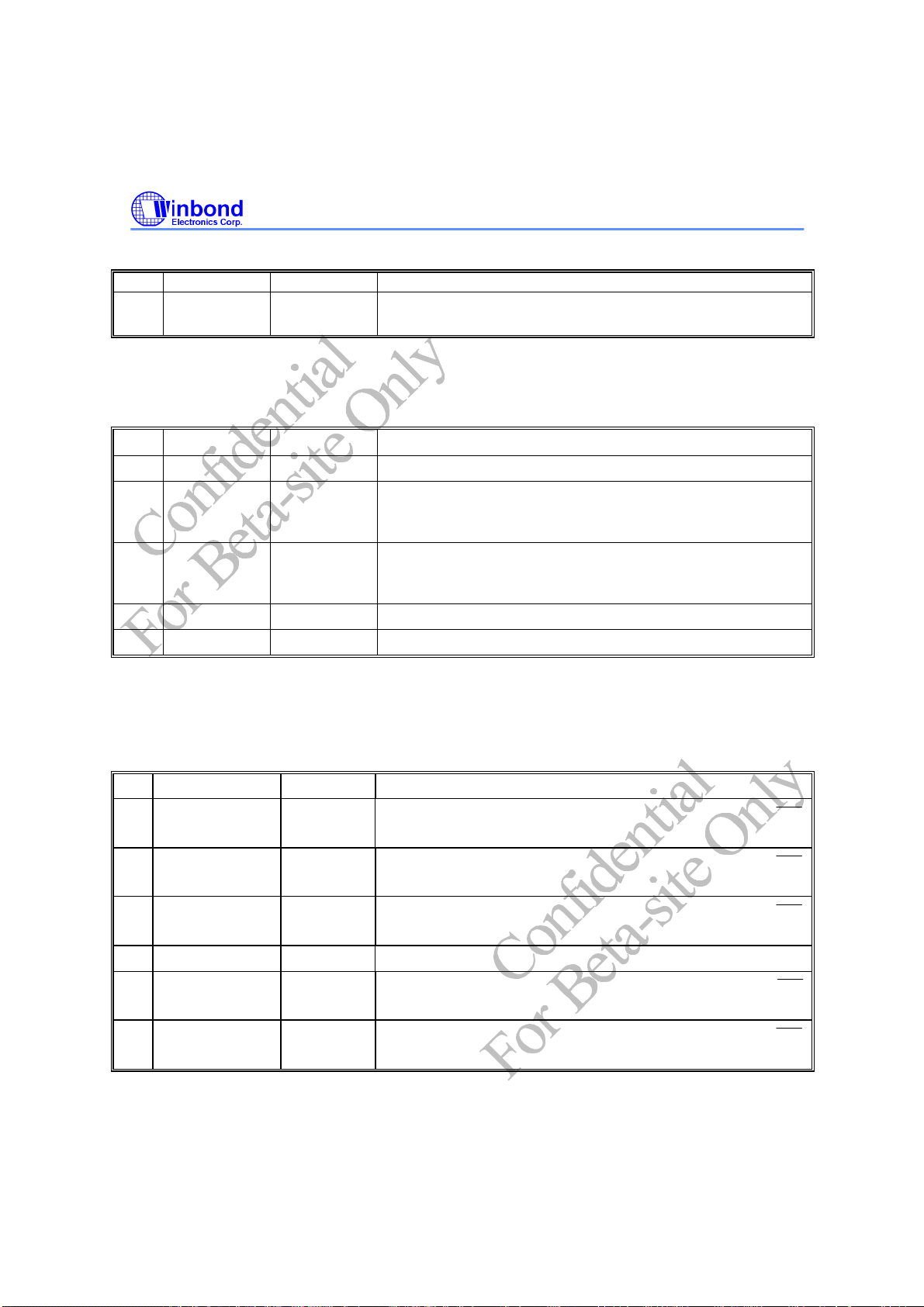
W83L784R
Preliminary
)
0 VCOIN Read Only A one indicates a High or Low limit has been exceeded.
(VIN1)
7.3 Interrupt Status Register 2 ¾ Index 42h
Power on default [7:0] = 0000,0000 b
Bit Name Read/Write Description
7-4 Reserved Read Only Read 0.
3 TAR_T2 Read Only CPUT2 Target Status.
with Fan 2 full speed can not be in the specific range after 3
minutes.
2 TAR_T1 Read Only CPUT1 Target Status.
with Fan 1 full speed can not be in the specific range after 3
minutes.
1 FAN2 Read Only A one indicates the fan count limit has been exceeded.
0 FAN1 Read Only A one indicates the fan count limit has been exceeded.
A one indicate CPUT2 temperature
A one indicate CPUT1 temperature
7.4 SMI Mask Register 1 ¾ Index 43h
Power on default <7:0> = 0000,0000 b
Bit Name Read/Write Description
7 MSK_T3_SMI Read/Write
6 MSK_T2_SMI Read/Write
5 MSK_T1_SMI Read/Write
Reserved Reserved Reserved
4
3 MSK_VCC_SMI Read/Write
2 MSK_3V_SMI Read/Write
A one disables the corresponding interrupt status bit for
interrupt.(CPUT2 target temperature)
A one disables the corresponding interrupt status bit for
interrupt.(CPUT1 target temperature)
A one disables the corresponding interrupt status bit for
interrupt. (internal thermal diode)
A one disables the corresponding interrupt status bit for
interrupt. (VCC, +5V)
A one disables the corresponding interrupt status bit for
interrupt. (Pin VIN2)
SMI
SMI
SMI
SMI
SMI
Confidential, For Beta-site Only Publication Release Date: Sep.
1999
-28 - Revision 0.54
Page 30
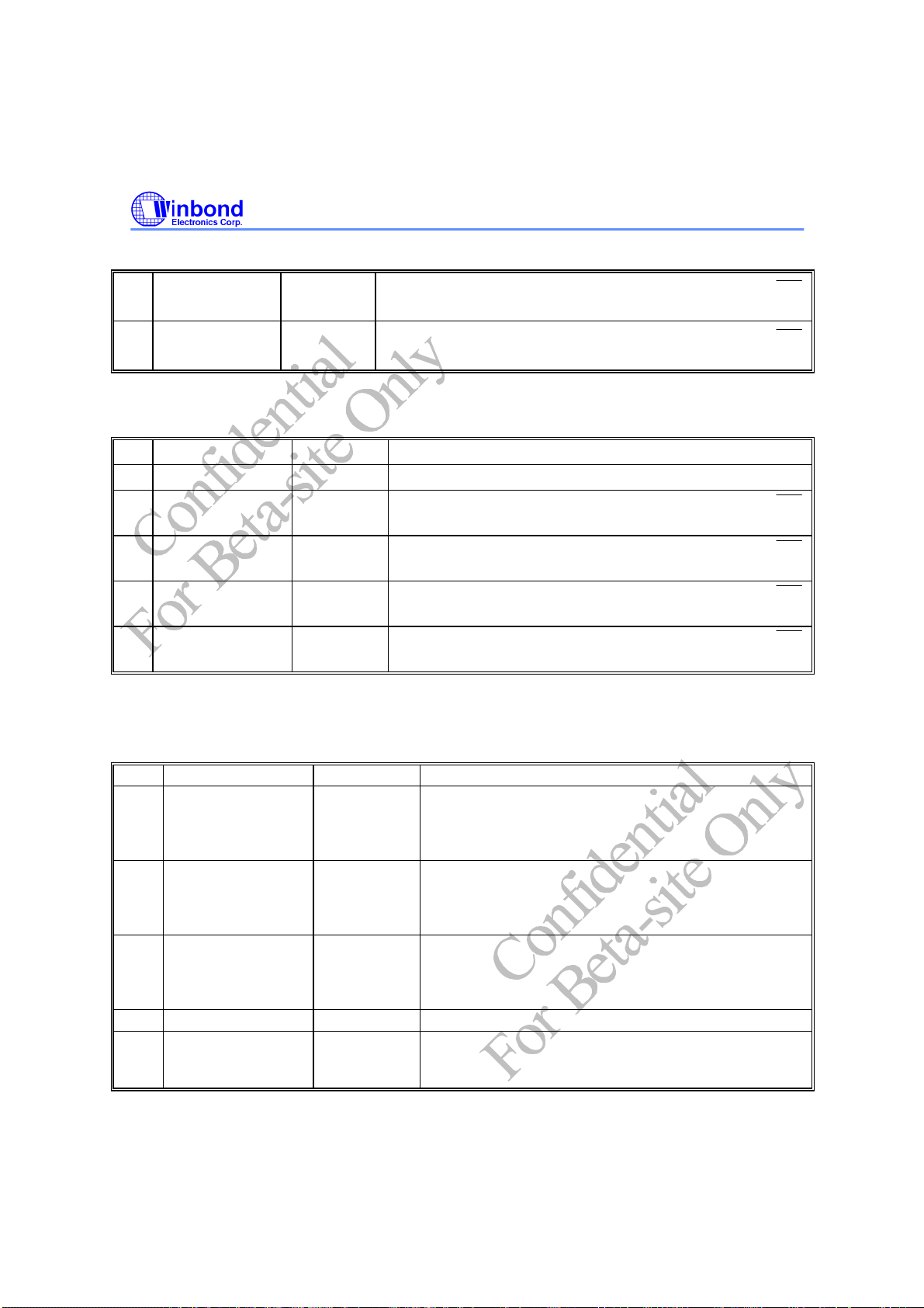
W83L784R
Preliminary
1 MSK_VBAT_S
MI
0 MSK_VCO_SMI Read/Write
Read/Write
A one disables the corresponding interrupt status bit for
interrupt.(Pin VIN3)
A one disables the corresponding interrupt status bit for
interrupt. (Pin VIN1)
7.5 SMIÝ Mask Register 2 ¾ Index 44h
Power on default [7:0] = 0000,0000 b
Bit Name Read/Write Description
7-4 Reserved
3 MSK_TAR2_SMI Read/Write
2 MSK_TAR1_SMI Read/Write
1 MSK_FAN2_SMI Read/Write
0 MSK_FAN1_SMI Read/Write
Read/Write Reserved.
A one disables the corresponding interrupt status bit for
interrupt. (CPUT2 target temperature )
A one disables the corresponding interrupt status bit for
interrupt. (CPUT1 target temperature )
A one disables the corresponding interrupt status bit for
interrupt. (Fan 2 speed counter)
A one disables the corresponding interrupt status bit for
interrupt. (Fan 1 speed counter)
7.6 Real Time Hardware Status Register I -- Index 45h
SMI
SMI
SMI
SMI
SMI
SMI
Power on - [7:0] = 0000,0000 b
Bit Name Read/Write Description
7 TEMP3_STS Read Only Temperature sensor 3 (CPU T2) Status. Set 1, the
voltage of temperature sensor is over the limit value.
Set 0, the voltage of temperature sensor is in the limit
range.
6 TEMP2_STS Read Only Temperature sensor 2 (CPU T1) Status. Set 1, the
voltage of temperature sensor is over the limit value.
Set 0, the voltage of temperature sensor is in the limit
range.
5 TEMP1_STS Read Only Temperature sensor 1 (Internal Thermal Diode) Status.
Set 1, the voltage of temperature sensor is over the
limit value. Set 0, the voltage of temperature sensor is
in the limit range.
4 Reserved Reserved Reserved.
3 VCCIN_STS Read Only +5V Voltage Status. Set 1, the voltage of +5V is over
the limit value. Set 0, the voltage of +5V is in the limit
range.
Confidential, For Beta-site Only Publication Release Date: Sep.
-29 - Revision 0.54
1999
Page 31
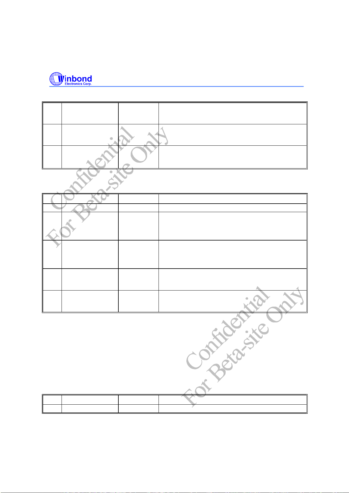
W83L784R
Preliminary
2 3V_STS Read Only +3.3V Voltage Status. Set 1, the voltage of +3.3V is
over the limit value. Set 0, the voltage of +3.3V is in the
limit range.
1 VBAT_STS Read Only VBAT (VIN3) Voltage Status. Set 1, the voltage of
VBAT(VIN3) is over the limit value. Set 0, the voltage
of VBAT(VIN3) is in the limit range.
0 VCO_STS Read Only VCORE A Voltage Status. Set 1, the voltage of VCORE
A is over the limit value. Set 0, the voltage of VCORE
A is in the limit range.
7.7 Real Time Hardware Status Register II -- Index 46h
Power on default [7:0] = 0000-0000 b
Bit Name Read/Write Description
7-4 Reserved Read Only Read 0.
3 TART2_STS Read Only CPUT2 Target Status.
temperature with Fan 2 full speed can not be in the
range after 3 minutes. Set 0, the temperature or speed
is in the specific range .
2 TART1_STS Read Only CPUT1 Targert Status.
temperature with Fan 1 full speed can not be in the
range after 3 minutes. Set 0, the temperature or speed
is in the specific range ..
1 FAN2_STS Read Only FAN 2 Status.
limit value. Set 0, the fan speed counter is in the limit
range.
0 FAN1_STS Read Only FAN 1 Status.
limit value. Set 0, the fan speed counter is in the limit
range.
Set 1, the fan speed counter is over the
Set 1, the fan speed counter is over the
Set 1, when CPUT2 target
Set 1, when CPUT1 target
7.8 Reserved Register -- Index 47h
Reserved.
7.9 Reserved Register -- Index 48h
Reserved.
7.10 Fan Divisor Register ¾ Index 49h
Power on default [7:4] = 0001,0001 b
Bit Name Read/Write Description
7 Reserved Read/write Reserved.
Confidential, For Beta-site Only Publication Release Date: Sep.
-30 - Revision 0.54
1999
Page 32
W83L784R
disable temperature 3 sensor and can not access any
Preliminary
6-4 F2_SP_CRTL[2:0] Read/Write
3 Reserved Read/write Reserved.
2-0 F1_SP_CTRL[2:0] Read/Write
FAN2 Speed Control.
000 - divide by 1;
001 - divide by 2;
010 - divide by 4;
011 - divide by 8.
100 - divide by 16.
101 - divide by 32.
110 - divide by 64.
111 - divide by 128.
FAN1 Speed Control.
000 - divide by 1;
001 - divide by 2;
010 - divide by 4;
011 - divide by 8.
100 - divide by 16.
101 - divide by 32.
110 - divide by 64.
111 - divide by 128.
7.11 Serial Bus Address (for Voltage ,Fan, and internal temperature ) Register ¾
Address 4Ah
Power on default [7:0] = 0010,1101 b
Bit Name Read/Write Description
7 Reserved
6-0 Serial Bus Address Read/Write Serial Bus address [6:0].
Read Only
7.12 CPUT1 Temperature and CPUT2 Temperature Serial Bus Address Register-Index 4Bh
Power on default [7:0] = 0000,0001 b
Bit Name Read/Write Description
7 DIS_CPUT2 Read/Write Disable CPUT2 Temperature Function.
Confidential, For Beta-site Only Publication Release Date: Sep.
-31 - Revision 0.54
Set to 1,
1999
Page 33
data from Temperature Sensor 3. Note that the relative
functions of Status, and SMI# will be disable.
6-4 I2CADDR3[2:0] Read/Write Temperature 3 Seiral Bus Address.
address is 1001xxx. Where xxx are defined in these
bits.
3 DIS_CPUT1
Read/write
Disable CPUT1 Temperature Function.
disable temperature Sensor and can not access any
data from Temperature Sensor 2. Note that the relative
functions of Status, and SMI# will be disable.
2-0 I2CADDR2[2:0]
Read/Write
Temperature 2 Serial Bus Address.
address is 1001xxx. Where xxx are defined in these
bits.
7.13 Winbond Vendor ID (Low Byte) - Index 4Ch (Auto Increase)
Power-on default [7:0] = 1010,0011 b (A3h)
Bit Name Read/Write Description
W83L784R
Preliminary
The serial bus
Set to 1,
The serial bus
7:0 VIDL[7:0] Read Only Vendor ID Low Byte. Default A3h.
7.14 Winbond Vendor ID (High Byte) - Index 4Dh (No Auto Increase)
Power-on default [7:0] = 0101,1100 b (5Ch)
Bit Name Read/Write Description
7:0
VIDH[7:0]
Read Only
Vendor ID High Byte.
Default 5Ch
7.15 Chip ID -- Index 4Eh
Power on default [7:0] = 0101,0000 b
Bit Name Read/Write Description
7-0 CHIPID[7:0] Read Only Winbond Chip ID number.
Read this register will
return 50h for W83L784R.
7.16 ACPI Temperature Increment Register -- Index 4Fh
Power on deafult [7:0] = 0000,0101 b
Bit Name Read/Write Description
7 Reserved Read/Write Reserved.
6-0 DIFFREG[6:0] ReadWrite ACPI Temperature Increment Register.
If set to this
Confidential, For Beta-site Only Publication Release Date: Sep.
1999
-32 - Revision 0.54
Page 34
W83L784R
through pin OVT#. The pin OVT# is wire OR with OVT2
Preliminary
register to non-zero value, the OVT# signal will be
actived at pointer of the temperaure of times of
DIFFREG (i.e. DIFFREG*n, where n is non-zero
integer). The default value is 5 degree C.
7.17 OVT# Property Select - Index 50h
Power on default [7:0] = 0000,0000 b
Bit Name Read/Write Description
7-6 Reserved Read/Write Reserved.
5-4 OVT_MD[1:0] Read/Write OVT# Mode Select.
type.
<00> -
activated until the temperature is less than T
<01> -
output activated indefinitely until reset reading temperature
sensor 1/2/3 registers. Temperature exceeding TO, then
OVT# reset, and then temperature going below T
also cause the OVT# activated indifinitely until reset by
reading temperature sensor 1/2/3. Onece the OVT# will not
be activated by exceeding TO, then reset, if the
temperature remains above T
actived agian.
<10> -
always send an OVT# signal when the temperature over
the ACPI temperature increment value defined at Index
4Fh.
3 EN_OVT3 Read/Write Enable CPUT2 temperature sensor over-temperature
(OVT) output if set to 1. Default 0, disable CPUT2 OVT
output through pin OVT#. The pin OVT# is wire OR with
OVT1 and OVT2.
2 EN_OVT2 Read/Write Enable CPUT1 temperature sensor over-temperature
(OVT) output if set to 1. Default 0, disable CPUT1 OVT
output through pin OVT#. The pin OVT# is wire OR with
OVT1 and OVT3.
1 EN_OVT1 Read/Write Enable internal temperature sensor over-temperature
(OVT) output if set to 1. Default 0, disable OVT1 output
Comparator Mode:
Temperature exceeding TO causes the OVT# output
Interrupt Mode:
Setting temperature exceeding TO causes the OVT#
ACPI Mode:
If set to 1 then enable ACPI OVT# output. Which is
There are three OVT# signal output
(Default)
.
HYST
, the OVT# will not be
HYST
HYST
will
Confidential, For Beta-site Only Publication Release Date: Sep.
1999
-33 - Revision 0.54
Page 35
and OVT3.
limit causes and interrupt and this interrupt will be reset
0 OVTPOL Read/Write Over-Temperature Polarity.
Write 0, OVT# active low. Default 0.
Write 1, OVT# active high.
7.18 SMI# Property Select -- Index 51h
Power on - <7:0> --0000,0100 b
Bit Name Read/Write Description
7-4 Reserved Read/Write Reserved.
3-2 TEMP_SMI_MD[1:0] Read/Write Temperature SMI Mode Select.
<00> -
Comparator Interrupt Mode:
Temperature 1/2/3 exceeds TO (Over-temperature)
W83L784R
Preliminary
1 EN_SMI# Read/Write Enable SMI# Output.
0 SMIPOL Read/Write SMI# Polarity.
by reading all the Interrupt Stauts.
<01> -
mode with hysteresis type. Temperature exceeding TO,
causes an interrupt and then temperature going below
T
has been reset by reading all the interrupt Status
Register. Once an interrupt event has occurred by
exceeding TO, then reset, if the temperature remains
above the T
<10>
mode with hysteresis type. Temperature exceeding TO
(Over-temperature, defined in Bank 1/2) causes an
interrupt and then temperature going below T
(Hysteresis temperature, defined in Bank 1/2) will not
cause an interrupt. Once an interrupt event has occurred
by exceeding TO, then going below T
will not occur again until the temperature exceeding TO.
output.
active low. Default 0.
Two Time Interrupt Mode:
This bit use in temperature sensor 1/2/3 interrupt
will also cause an interrupt if the previous interrupt
HYST
.
HYST
- One Time Interrupt Mode:
This bit use in temperature sensor 1/2/3 interrupt
A one enables the SMI# Interrupt
Write 1, SMI# active high. Write 0, SMI#
(Default)
, and interrupt
HYST
HYST
7.19 FANIN1/GPO1, FANIN2/GPO2 and BEEP/GPO3 Control Register- Indxe 52h
Confidential, For Beta-site Only Publication Release Date: Sep.
-34 - Revision 0.54
1999
Page 36
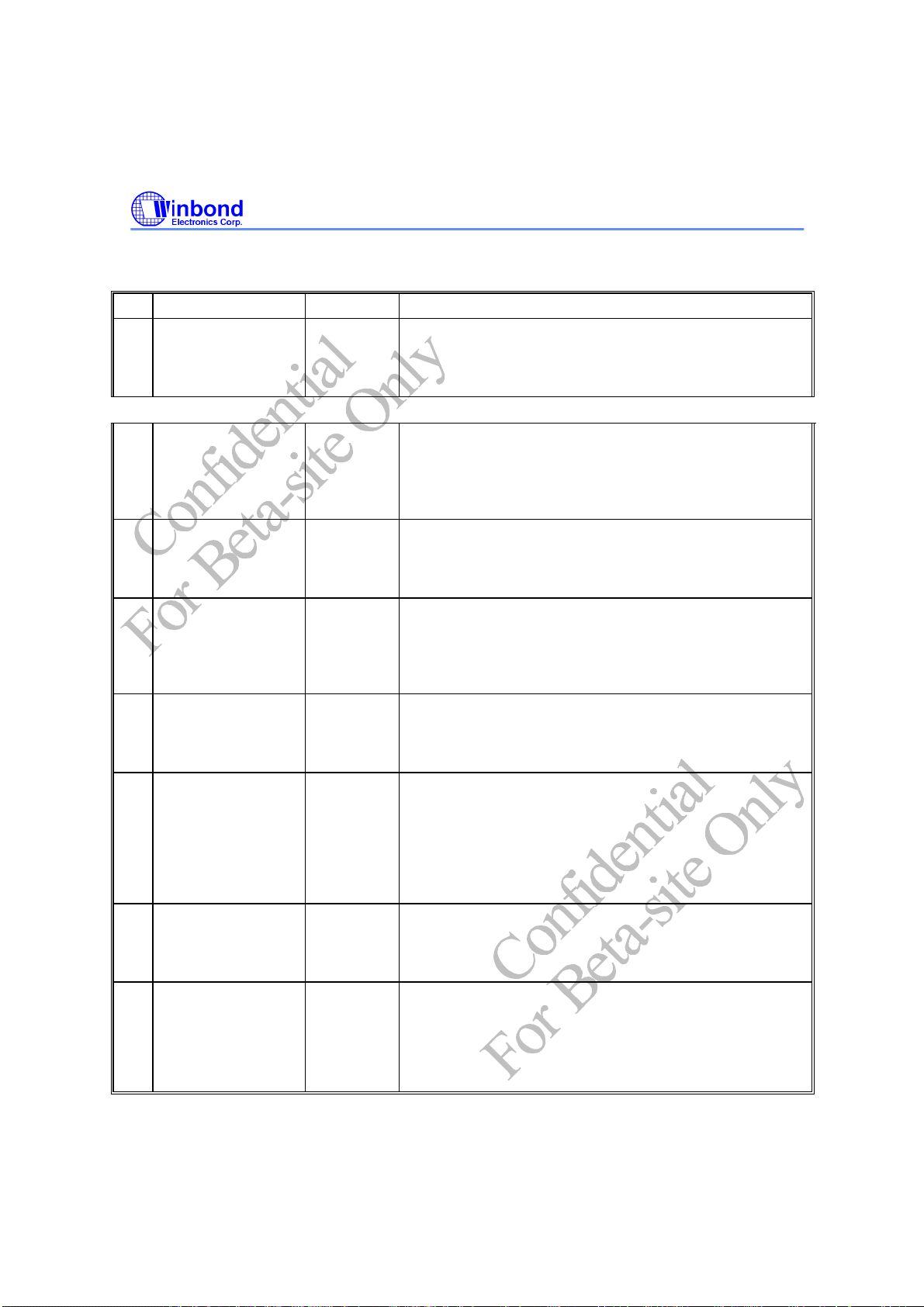
Power on default [7:0] = 0000,0000 b
this register bit 1. This output pin GPO2 can connect to
Bit Name Read/Write Description
W83L784R
Preliminary
7 GPO4_VAL Read/Write GPO4 Output Value.
set to 1. Write 1, then pin 11 (GPO4) always generate logic
high signal. Write 0, pin 11 (GPO4) always generates logic
low signal. This bit default 0.
FANIN1/GPO1, FANIN2/GPO2 and BEEP/GPO3 Control Register- Indxe 52h.
6 EN_GPO4 Read/Wite Enable GPO4 Function.
(BATFAULT#/GPO3) acts as BATFAULT# whcih is battery
voltage out of the limit value. Set to 1, this pin 11 acts as
GPO4 control function and the output value of GPO4 is
programmed by this register bit 7.
5 GPO3_VAL Read/Write GPO3 Output Value.
set to 1. Write 1, then pin 5 (GPO3) always generate logic
high signal. Write 0, pin 5 (GPO3) always generates logic
low signal. This bit default 0.
4 EN_GPO3 Read/Wite Enable GPO3 Function.
(FANFAULT#/GPO3) acts as FAN_FAULT whcih is fan
count out of the limit value. Set to 1, this pin 5 acts as
GPO3 control function and the output value of GPO3 is
programmed by this register bit 5.
3 GPO2_VAL Read/Write GPO2 Output Value.
set to 1. Write 1, then pin 2 (GPO2) always generate logic
high signal. Write 0, pin 2 (GPO2) always generates logic
low signal. This bit default 0.
2 EN_GPO2 Read/Write Enable GPO2 Function.
pin 2, named FANIN2/GPO2, GPO2 function. Set to 0
(default), pin 2 (FANIN2/GPO2) acts as FANIN2 whcih is
fan clock input. Set to 1, this pin 2 acts as GPO2 control
function and the output value of GPO2 is programmed by
this register bit 3. This output pin GPO2 can connect to
power PMOS gate to control FAN ON/OFF.
1 GPO1_VAL Read/Write GPO1 Output Value.
set to 1. Write 1, then pin 1 (GPO1) always generate logic
high signal. Write 0, pin 1 (GPO1) always generates logic
low signal. This bit default 0.
0 EN_GPO1
Read/Write Enable GPO1 Function.
pin 1, named FANIN1/GPO1, GPO1 function. Set to 0
(default), pin 1 (FANIN1/GPO1) acts as FANIN1 whcih is
fan clock input. Set to 1, this pin 1 acts as GPO1 control
function and the output value of GPO1 is programmed by
GPO4 output value if EN_GPO4 is
Set to 0 (default), pin 11
GPO3 output value if EN_GPO3 is
Set to 0 (default), pin 5
GPO2 output value if EN_GPO2 is
Which enable multiple function
GPO1 output value if EN_GPO1 is
Which enable multiple function
Confidential, For Beta-site Only Publication Release Date: Sep.
1999
-35 - Revision 0.54
Page 37
power PMOS gate to control FAN ON/OFF.
Swap CPUT2 PWM to internal temperature sensor
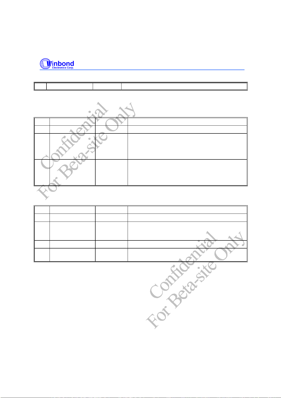
7.20 CPUT1/CPUT2 Thermal Sensor Type Register -- Index 53h
Power on default [7:0] = 0000-0000 b
Bit Name Read/Write Description
7-4 Reserved Read/Write Reserved.
3-2 T3_TYPE[1:0] Read/Write Temperature sensor 3 (CPU T2) type.
0x - Thermistor (10K @ 25 degree C, B=3435).
10 - 2N3904 transistor.
11 - Intel thermal diode.
1-0 T2_TYPE[1:0] Read/Write Temperature sensor 2 (CPU T1) type.
0x - Thermistor (10K @ 25 degree C, B=3435)
10 - 2N3904 transistor
11 - Intel thermal diode.
W83L784R
Preliminary
7.21 Misc Control Register -- Index 54h
Power on default [7:0] = 0000-0000 b
Bit Name Read/Write Description
7-3 Reserved Read/Write Reserved.
2 SWP_FAN2_PWM Read/Write
1 Reserved Reserved Reserved
0 EN_VBAT_MNT ReadWrite Write 1, enable battery voltage monitor. Write 0,
PWM Control.
control will refer to internal temperature senesor.
disable battery voltage monitor. (VIN4/VBAT)
Write this bit set to 1, FAN2 PWM PWM
Confidential, For Beta-site Only Publication Release Date: Sep.
1999
-36 - Revision 0.54
Page 38
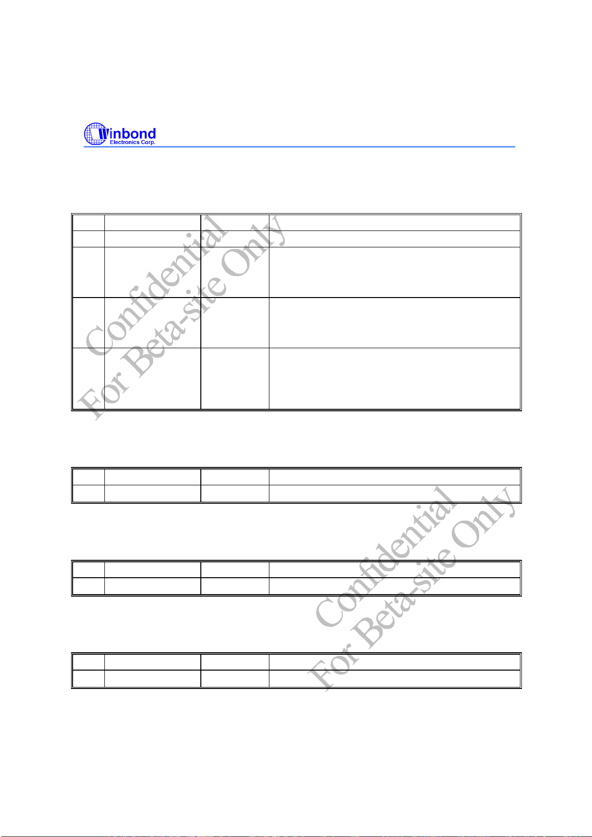
7.22 Fan/VBAT Fault Control Register -- Index 55h
Power on default [7:0] = 0000-0000 b
Bit Name Read/Write Description
7-3 Reserved Read/Write Reserved.
2 EN_FAN2_FAULT Read/Write Enable Fan 2 Fault Function.
the Fan Fault Limit value (defined Index 58 and 59), the
Pin 5 will go to low level. This function is wire-or with
Fan 1 fault if fan 1 fualt function is enable.
1 EN_FAN1_FAULT Read/Write Enable Fan1 Fault Function.
Fan Fault Limit value (defined Index 56 and 57), the
Pin 5 will go to low level. This function is wire-or with
Fan 2 fault if fan 2 fualt function is enable.
0 EN_VBAT_FAULT ReadWrite Enable VBAT Fault Function
fault function. Set to 0, disable this function. When
battery voltage is out of the fault limit value (defined at
Index 5A and 5B), the Pin 11 (BATFAULT#) will be
asserted.
W83L784R
Preliminary
When Fan 2 is out of
When Fan 1 is out of the
. Set to 1, enable battery
7.23 Fan 1 Fault High Limit Count -- Index 56h
Power on default [7:0] = 1111-1111 b
Bit Name Read/Write Description
7-0 FAN_HI_LM Read/Write Fan High Count Limit Value.
7.24 Fan 2 Fault Low Limit Count -- Index 57h
Power on default [7:0] = 0000-0000 b
Bit Name Read/Write Description
7-0 FAN_LOW_LM Read/Write Fan Low Count Limit Value.
7.25 Fan 2 Fault High Limit Count -- Index 58h
Power on default [7:0] = 1111-1111 b
Bit Name Read/Write Description
7-0 FAN_HI_LM Read/Write Fan High Count Limit Value.
Confidential, For Beta-site Only Publication Release Date: Sep.
1999
-37 - Revision 0.54
Page 39
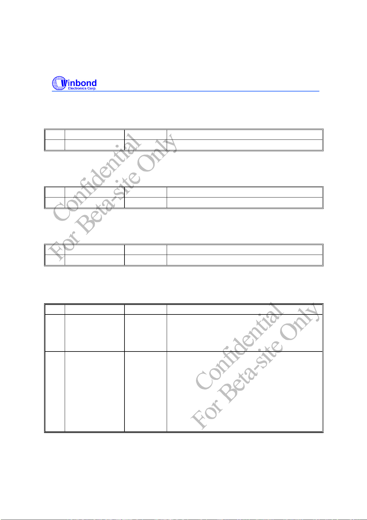
7.26 Fan 1 Fault Low Limit Count -- Index 59h
Power on default [7:0] = 0000-0000 b
Bit Name Read/Write Description
7-0 FAN_LOW_LM Read/Write Fan Low Count Limit Value.
7.27 VBAT Fault High Limit Value -- Index 5Ah
Power on default [7:0] = 1111-1111 b
Bit Name Read/Write Description
7-0 VBAT_HI_LM Read/Write VBAT High Limit Value.
7.28 VBAT Fault Low Limit Value -- Index 5Bh
Power on default [7:0] = 0000-0000 b
Bit Name Read/Write Description
W83L784R
Preliminary
7-0 VBAT_LOW_LM Read/Write VBAT Low Limit Value.
7.29 FAN 1 Pre-Scale Register-- Index 80h
Power on default [7:0] = 0000-0001 b
Bit Name Read/Write Description
7 PWM_CLK_SEL1 Read/Write PWM Input Clock Select.
clock to pre-scale divider.
0: 1 MHz
1: 125 KHz
6-0 PRE_SCALE1[6:0] Read/Write Fan 1 Input Clock Pre-Scale.
clock is the number defined by pre-scale. Thus, writing
0 transfers the input clock directly to counter. The
maximum divider is 128 (7Fh).
00h : divider is 1
01h : divider is 2
02h : divider is 3
:
:
This bit select Fan 1 input
The divider of input
Confidential, For Beta-site Only Publication Release Date: Sep.
1999
-38 - Revision 0.54
Page 40
W83L784R
Preliminary
7.30 FAN 1 Duty Cycle Select Register-- 81h (
Power on default [7:0] 1111,1111 b
Bit Name Read/Write Description
7-0 F1_DC[7:0] Read/Write Fan 1 Duty Cycle.
number of input clock cycles, out of 256-cycle period,
during which the PWM output is high. During smart fan
1 control mode, read this register will return smart fan
duty cycle.
00h: PWM output is always logical Low.
FFh: PWM output is always logical High.
XXh: PWM output logical High percentage is
(XX/256*100%) during one cycle.
Bank 0
)
This 8-bit register determines the
7.31 FAN 2 Pre-Scale Register-- Index 82h
Power on default [7:0] = 0000,0001 b
Bit Name Read/Write Description
7 PWM_CLK_SEL2 Read/Write PWM 2 Input Clock Select.
clock to pre-scale divider.
0: 1 MHz
1: 125 KHz
6-0 PRE_SCALE2[6:0] Read/Write Fan 2 Input Clock Pre-Scale.
clock is the number defined by pre-scale. Thus, writing
0 transfers the input clock directly to counter. The
maximum divider is 128 (7Fh).
00h : divider is 1
01h : divider is 2
02h : divider is 3
:
:
This bit select Fan 2 input
The divider of input
Confidential, For Beta-site Only Publication Release Date: Sep.
-39 - Revision 0.54
1999
Page 41
7.32 FAN2 Duty Cycle Select Register-- Index 83h
Power on default [7:0] = 1111,1111 b
Bit Name Read/Write Description
W83L784R
Preliminary
7-0 F2_DC[7:0] Read/Write Fan 2 Duty Cycle.
number of input clock cycles, out of 256-cycle period,
during which the PWM output is high. During smart fan
2 control mode, read this register will return smart fan
duty cycle.
00h: PWM output is always logical Low.
FFh: PWM output is always logical High.
XXh: PWM output logical High percentage is
XX/256*100% during one cycle.
This 8-bit register determines the
7.33 FAN Configuration Register-- Index 84h
Power on default [7:0] = 0000,0000 b
Bit Name Read/Write Description
7-2 Reserved Read/Write Reserved
5-4 FAN2_MODE Read/Write FAN 2 PWM Control Mode.
00 - Manual PWM Control Mode. (Default)
01 - Thermal Cruise mode.
10 - Fan Speed Cruise Mode.
11 - Reserved.
3-2 FAN1_MODE Read/Write FAN 1 PWM Control Mode.
00 - Manual PWM Control Mode. (Default)
01 - Thermal Cruise mode.
10 - Fan Speed Cruise Mode.
11 - Reserved.
1 FAN2_OB Read/Write Enable Fan 2 as Output Buffer.
can drive logical high or logical low. Default Pin 4
(FANPWM) is open-drain.
Confidential, For Beta-site Only Publication Release Date: Sep.
-40 - Revision 0.54
Set to 1, FANPWM1
1999
Page 42
W83L784R
Only for Thermal Cruise
Only for Thermal Cruise
Preliminary
0 FAN1_OB Read/Write Enable Fan 1 as Output Buffer.
can drive logical high or logical low. Default Pin 3
(FANPWM) is open-drain.
Set to 1, FANPWM1
7.34 CPUT1 Target Temperature Register/ Fan 1 Target Speed Register -- Index 85h
Power on default [7:0] = 0000,0000 b
CPUT1 target temperature register for Thermal Cruise mode.
Bit Name Read/Write Description
7 Reserved Read/Write Reserved.
6-0 TEMP_TAR_T1[6:0] Read/Write CPUT1 Target Temperature.
Fan 1 target speed register for Fan Speed Cruise mode.
Bit Name Read/Write Description
7-0 SPD_TAR_FAN1[7
:0]
Read/Write Fan 1 Target Speed Control.
Mode while CR84h bit3-2 is 01.
Only for Fan Speed
Cruise Mode while CR84h bit3-2 is 10.
7.35 CPUT2 Target Temperature Register/ Fan 2 Target Speed Register -- Index 86h
Power on - [7:0] = 0000,0000 b
CPUT2 target temperature register for Thermal Cruise mode.
Bit Name Read/Write Description
7 Reserved Read/Write Reserved.
6-0 TEMP_TAR_T2[6:0] Read/Write CPUT1 Target Temperature.
Fan 2 target speed register for Fan Speed Cruise mode.
Bit Name Read/Write Description
7-0 SPD_TAR_FAN2[7:
0]
Confidential, For Beta-site Only Publication Release Date: Sep.
Read/Write Fan 1 Target Speed Control.
Mode while CR84h bit5-4 is 01.
Only for Fan Speed
Cruise Mode while CR84h bit5-4 is 10.
-41 - Revision 0.54
1999
Page 43
W83L784R
Preliminary
7.36 Tolerance of Target Temperature or Target Speed Register -- Index 87h
Power on default [7:0] = 0001,0001 b
Tolerance of CPUT1/CPUT2 target temperature register.
Bit Name Read/Write Description
7-4 TOL_T2[3:0] Read/Write Tolerance of Fan 2 Target Temperature.
Thermal Cruise mode.
3-0 TOL_T1[3:0] Read/Write Tolerance of Fan 1 Target Temperature.
Thermal Cruise mode.
Tolerance of Fan 1/2 target speed register.
Bit Name Read/Write Description
7-4 TOL_FS2[3:0] Read/Write Tolerance of Fan 2 Target Speed Count.
Fan Speed Cruise mode.
3-0 TOL_FS1[3:0] Read/Write Tolerance of Fan 1 Target Speed Count.
Fan Speed Cruise mode.
Only for
Only for
Only for
Only for
7.37 Fan 1 PWM Stop Duty Cycle Register -- Index 88h
Power on default [7:0] = 0000,0001 b
Bit Name Read/Write Description
7-0 STOP_DC1[7:0] Read/Write In Thermal Cruise mode, PWM duty will be 0 if it
decreases to under this value. This register should be
written a non-zero minimum PWM stop duty cycle.
7.38 Fan 2 PWM Stop Duty Cycle Register -- 89h (
Power on default [7:0] = 0000,0001 b
Bit Name Read/Write Description
7-0 STOP_DC2[7:0] Read/Write In Thermal Cruise mode, PWM duty will be 0 if it
decreases to under this register value. This register
should be written a non-zero minimum PWM stop duty
cycle.
Bank 0
)
7.39 Fan 1 Start-up Duty Cycle Register -- Index 8Ah
Confidential, For Beta-site Only Publication Release Date: Sep.
1999
-42 - Revision 0.54
Page 44
W83L784R
Preliminary
Power on default [7:0] = 0000,0001 b
Bit Name Read/Write Description
7-0 START_DC1[7:0] Read/Write In Thermal Cruise mode, PWM duty will increase from
0 to this register value to provide a minimum duty cycle
to turn on the fan. This register should be written a fan
start-up duty cycle.
7.40 Fan 2 Start-up Duty Cycle Register -- Index 8Bh
Power on default [7:0] = 0000,0001 b
Bit Name Read/Write Description
7-0 START_DC2[7:0] Read/Write In Thermal Cruise mode, PWM duty will increase from
0 to this register value to provide a minimum duty cycle
to turn on the fan. This register should be written a fan
start-up duty cycle.
7.41 Fan 1 Stop Time Register -- Indxe 8Ch
Power on default [7:0] = 0011,1100 b
Bit Name Read/Write Description
7-0 STOP_TIME1[7:0] Read/Write In Thermal Cruise mode, this register determines the
time of which PWM duty is from stop duty cycle to 0
duty cycle. The unit of this register is 0.1 second. The
default value is 6 seconds.
7.42 Fan 2 Stop Time Register -- Index 8Dh
Power on default [7:0] = 0011,1100 b
Bit Name Read/Write Description
7-0 STOP_TIME2[7:0] Read/Write In Thermal Cruise mode, this register determines the
time of which PWM duty is from stop duty cycle to 0
duty cycle. The unit of this register is 0.1 second. The
default value is 6 seconds.
7.43 Fan Step Down Time Register -- Index 8Eh
Power on defualt [7:0] = 0000,1010 b
Confidential, For Beta-site Only Publication Release Date: Sep.
1999
-43 - Revision 0.54
Page 45
Bit Name Read/Write Description
The time interval, which is 0.1 second unit, to decrease
The time interval, which is 0.1 second unit, to increase
7-0 STEP_UP_T[7:0] Read/Write
7.44 Fan Step Up Time Register -- Index 8Fh
Power on default [7:0] = 0000,1010 b
Bit Name Read/Write Description
7-0 STEP_DOWN_T[7:0] Read/Write
7.45 Temperature Sensor 1 (Internal Thermal Diode) Offset Register - Index 90h
W83L784R
Preliminary
PWM duty in Smart Fan Control mode.
PWM duty in Smart Fan Control mode.
Power-on default [7:0] = 0000,0000 b
Bit Name Read/Write Description
7-6 Reserved Read/Write Reserved.
5-0 OFFSET1[5:0] Read/Write Temperature 1 base temperature. This value is added
to monitor value, resulting in the current temperature.
01,1111 => +31 degree C
01,1110 => +30 degree C
:
00,0001 => +1 degree C
00,0000 => +0 degree C
11,1111 => -1 degree C
11,1110 => -2 degree C
:
10,0000 => -32 degree
7.46 Temperature Sensor 2 (CPU T1) Offset Register - Index 91h
Power-on default [7:0] = 0000,0000 b
Bit Name Read/Write Description
Confidential, For Beta-site Only Publication Release Date: Sep.
1999
-44 - Revision 0.54
Page 46
W83L784R
Preliminary
7-6 Reserved Read/Write Reserved.
5-0 OFFSET1[5:0] Read/Write Temperature 2 (CPUT1) base temperature. This
value is added to monitor value, resulting in the
current temperature.
01,1111 => +31 degree C
01,1110 => +30 degree C
:
00,0001 => +1 degree C
00,0000 => +0 degree C
11,1111 => -1 degree C
11,1110 => -2 degree C
:
10,0000 => -32 degree
7.47 Temperature Sensor 3 (CPU T2) Offset Register - Index 92h
Power-on default [7:0] = 0000,0000 b
Bit Name Read/Write Description
7-6 Reserved Read/Write Reserved.
5-0 OFFSET3[5:0] Read/Write Temperature 3 (CPU T2) base temperature. This
value is added to monitor value, resulting in the
current temperature.
01,1111 => +31 degree C
01,1110 => +30 degree C
:
00,0001 => +1 degree C
00,0000 => +0 degree C
11,1111 => -1 degree C
11,1110 => -2 degree C
:
10,0000 => -32 degree
Confidential, For Beta-site Only Publication Release Date: Sep.
1999
-45 - Revision 0.54
Page 47
8. VALUE RAM AND LIMIT VALUE
8.1 Value RAM ¾ Index 20h- 3Fh or 60h - 7Fh
Index A6-A0 Index A6-A0 Description
20h
21h
22h 62h Pin VIN2 reading (+3.3V)
23h 63h Pin VCC reading (VCC,+5V)
24h 64h Reserved
25h 65h Reserved
26h 66h Reserved
27h 67h Internal Temperature reading
28h 68h FAN1 reading
29h 69h FAN2 reading
2Ah 6Ah Reserved
2Bh 6Bh VIN1(Vcore) High Limit
2Ch 6Ch VIN1(Vcore) Low Limit
2Dh 6Dh VIN3 (VBAT) High Limit
2Eh 6Eh VIN3 (VBAT) Low Limit
2Fh 6Fh VIN2 (+3.3V) High Limit
30h 70h VIN2 (+3.3V) Low Limit
60h
61h
Pin VIN1 reading (Vcore)
Pin VIN3 reading (VBAT)
Note:
This location stores the number of counts of the
internal clock per revolution.
Note:
This location stores the number of counts of the
internal clock per revolution.
W83L784R
Preliminary
Confidential, For Beta-site Only Publication Release Date: Sep.
1999
-46 - Revision 0.54
Page 48
W83L784R
Preliminary
31h 71h VCC High Limit
32h 72h VCC Low Limit
33h 73h Reserved
34h 74h Reserved
35h 75h Reserved
36h 76h Reserved
37h 77h Reserved
38h 78h Reserved
39h 79h Over Temperature Limit (High) of internal temperature
3Ah 7Ah Temperature Hysteresis Limit (Low) of internal
3Bh 7Bh FAN1 Fan Count Limit
3Ch
3Dh
3E- 3Fh 7E- 7Fh Reserved
7Ch
7Dh
temperature
FAN2 Fan Count Limit.
Reserved
Confidential, For Beta-site Only Publication Release Date: Sep.
1999
-47 - Revision 0.54
Page 49
9. TEMPERATURE SENSOR 2 (CPU T1) REGISTERS
The address of I2C is defined in Bank0.Reg4B.
9.1 Temperature Sensor 2 Temperature Register - Index 00h
Read Only
Bit Name Read/Write Description
15-7 TEMP2[8:0]
6-0
Reserved
Read Only
Read Only
9.2 Temperature Sensor 2 Configuration Register - Index 01h
Power-on default [7:0] = 0000,0000 b
Bit Name Read/Write Description
Temperature bit [8:0] of sensor 2. (0.5 degree C
precision)
Read 0.
W83L784R
Preliminary
7-5 Reserved Read Read 0.
4-3 FAULT Read/Write Number of faults to detect before setting OVT# output
to avoid false tripping due to noise.
2-1 Reserved Read/Write Reserved.
0
Reserved
Read/Write Reserved.
9.3 Temperature Sensor 2 Hysteresis Register - Index 02h
Power-on - <15:0> = 0100,1011,0000,0000 b
Bit Name Read/Write Description
15-7 THYST2[8:0]
Read/Write Temperature hysteresis bit 8-0. The temperature
default 75.0 degree C.
6:0 Reserved Read Read 0.
9.4 Temperature Sensor 2 Over-temperature Register - Index 03h
Power-on - <15:0> = 0101,0000,0000,0000 b
Bit Name Read/Write Description
15-7 TOVF2[8:0]
6:0 Reserved Read Read 0.
Read/Write Over-temperature bit 8-0. The temperature default
80.0 degree C.
Confidential, For Beta-site Only Publication Release Date: Sep.
1999
-48 - Revision 0.54
Page 50
10. TEMPERATURE SENSOR 3 (CPU T2) REGISTERS
The address of I2C is defined in Bank0.Reg4B.
10.1 Temperature Sensor 3 Temperature Register - Index 00h
Read Only
Bit Name Read/Write Description
15-7 TEMP2[8:0]
Read Only
6-0 Reserved Read Only Read 0.
10.2 Temperature Sensor 3 Configuration Register - Index 01h
Power-on - [7:0] = 0000,0000 b
Bit Name Read/Write Description
Temperature bit [8:0] of sensor 2. (0.5 degree C
precision).
W83L784R
Preliminary
7-5 Reserved Read Read 0.
4-3 FAULT Read/Write Number of faults to detect before setting OVT# output
to avoid false tripping due to noise.
2-1 Reserved Read Only Read 0.
0
Reserved
Read/Write Reserved
10.3 Temperature Sensor 3 Hysteresis Register - Index 02h
Power-on default [15:0] = 0100,1011,0000,0000 b
Bit Name Read/Write Description
15-7 THYST3[8:0]
Read/Write Temperature hysteresis bit 8-0. The temperature
default 75.0 degree C.
6-0 Reserved Read Only Read 0.
10.4 Temperature Sensor 3 Over-temperature Register - Index 03h
Power-on - [15:0] = 0101,0000,0000,0000 b
Bit Name Read/Write Description
15-7 TOVF3[8:0]
6-0 Reserved Read Only Read 0.
Read/Write Over-temperature bit 8-0. The temperature default
80.0 degree C.
Confidential, For Beta-site Only Publication Release Date: Sep.
1999
-49 - Revision 0.54
Page 51
W83L784R
Preliminary
11. SPECIFICATIONS
11.1 Absolute Maximum Ratings
PARAMETER RATING UNIT
Power Supply Voltage -0.5 to 7.0 V
Input Voltage -0.5 to VDD+0.5 V
Operating Temperature 0 to +70
Storage Temperature -55 to +150
Note: Exposure to conditions beyond those listed under Absolute Maximum Ratings may adversely affect the life and reliability of the
device.
11.2 DC Characteristics
(Ta = 0° C to 70° C, V
DD
= 5V ± 10%, VSS = 0V)
°
C
° C
PARAMETER SYM. MIN. TYP. MAX. UNIT CONDITIONS
I/O
- TTL level bi-directional pin with source-sink capability of 12 mA
12t
Input Low Voltage VIL 0.8 V
Input High Voltage VIH 2.0 V
OL
Output Low Voltage VOL 0.4 V I
Output High Voltage VOH 2.4 V I
Input High Leakage I
Input Low Leakage I
I/O
- TTL level bi-directional pin with source-sink capability of 12 mA and schmitt-trigger level
12ts
LIH
+10
LIL
-10
µ
A
µ
A
= 12 mA
OH
= - 12 mA
VIN = VDD
VIN = 0V
input
Input Low Threshold Voltage Vt- 0.5 0.8 1.1 V VDD = 5 V
Input High Threshold Voltage Vt+ 1.6 2.0 2.4 V VDD = 5 V
Hysteresis VTH 0.5 1.2 V VDD = 5 V
OL
Output Low Voltage VOL 0.4 V I
Output High Voltage VOH 2.4 V I
Input High Leakage I
Input Low Leakage I
LIH
+10
LIL
-10
µ
A
µ
A
= 12 mA
OH
= - 12 mA
VIN = VDD
VIN = 0V
Confidential, For Beta-site Only Publication Release Date: Sep.
1999
-50 - Revision 0.54
Page 52
W83L784R
Preliminary
11.2 DC Characteristics, continued
PARAMETER SYM. MIN. TYP. MAX. UNIT CONDITIONS
OUT
- TTL level output pin with source-sink capability of 12 mA
12t
OL
Output Low Voltage VOL 0.4 V I
Output High Voltage VOH 2.4 V I
OD8 - Open-drain output pin with sink capability of 8 mA
Output Low Voltage VOL 0.4 V I
OD12 - Open-drain output pin with sink capability of 12 mA
Output Low Voltage VOL 0.4 V I
OD48 - Open-drain output pin with sink capability of 48 mA
Output Low Voltage VOL 0.4 V I
INt - TTL level input pin
Input Low Voltage VIL 0.8 V
Input High Voltage VIH 2.0 V
Input High Leakage I
Input Low Leakage I
LIH
+10
LIL
-10
µ
A
µ
A
INts - TTL level Schmitt-triggered input pin
= 12 mA
OH
= -12 mA
OL
= 8 mA
OL
= 12 mA
OL
= 48 mA
VIN = VDD
VIN = 0 V
Input Low Threshold Voltage Vt- 0.5 0.8 1.1 V VDD = 5 V
Input High Threshold Voltage Vt+ 1.6 2.0 2.4 V VDD = 5 V
Hysteresis VTH 0.5 1.2 V VDD = 5 V
Input High Leakage I
Input Low Leakage I
LIH
+10
LIL
-10
A
A
VIN = VDD
VIN = 0 V
µ
µ
Confidential, For Beta-site Only Publication Release Date: Sep.
-51 - Revision 0.54
1999
Page 53
11.3 AC Characteristics
11.3.1 Serial Bus Timing Diagram
SCL
t
HD;SDA
W83L784R
Preliminary
t
SCL
t
HD;DAT
t
SU;STO
SDA IN
SDA OUT
VALID DATA
t
SU;DAT
Serial Bus Timing Diagram
Serial Bus Timing
PARAMETER SYMBOL MIN. MAX. UNIT
SCL clock period t
Start condition hold time t
Stop condition setup-up time t
DATA to SCL setup time t
DATA to SCL hold time t
-
10 uS
SCL
4.7 uS
HD;SDA
4.7 uS
SU;STO
120 nS
SU;DAT
5 nS
HD;DAT
SCL and SDA rise time tR 1.0 uS
SCL and SDA fall time tF 300 nS
Confidential, For Beta-site Only Publication Release Date: Sep.
1999
-52 - Revision 0.54
Page 54
12. HOW TO READ THE TOP MARKING
The top marking of W83L784R
W83L784R
2826978Y-61
814OB
Left: Winbond logo
1st line: Winbond logo and the type number: W83L784R
2nd line: Tracking code 2 826978Y-61
2
B: IC revision
826978Y-61
3rd line: Tracking code 814 O B
O: assembly house ID; A means ASE, S means SPIL, O means OSE
: wafers manufactured in Winbond FAB 2
: wafer production series lot number
814
: packages made in '98, week 14
W83L784R
Preliminary
Confidential, For Beta-site Only Publication Release Date: Sep.
1999
-53 - Revision 0.54
Page 55
13. PACKAGE DRAWING AND DIMENSIONS
2
20 SSOP-209 mil
D
11
DTEAIL A
H
E
E
SEATING PLANE
Y
1
e
b
10
A2 A
A1
DETAIL A
SEATING PLANE
q
L
L1
SYMBOL
A
A1
A2
b
c
D
E
H
e
L
L1
Y
q
DIMENSION IN MM
MIN. NOM MAX. MAX.NOM
2.00
0.05
0.22 0.38
0.09 0.25
6.90
5.00
7.40
E
0.55 0.75
0
1.85
1.751.65
7.50
7.20
5.30
5.60
7.80
8.20
0.65
0.95 0.037
1.25
0.10
8
W83L784R
Preliminary
DIMENSION IN INCH
MIN.
0.079
0.002
0.065
0.069
0.073
0.009 0.015
0.004 0.010
0.272 0.2950.283
0.197
0.291
0.021 0.030
0
0.209
0.0256
0.050
0.220
0.3230.307
0.004
8
Headquarters
No. 4, Creation Rd. III
Science-Based Industrial Park
Hsinchu, Taiwan
TEL: 886-35-770066
FAX: 886-35-789467
www: http://www.winbond.com.tw/
Winbond Electronics (H.K.) Ltd.
Rm. 803, World Trade Square, Tower II
123 Hoi Bun Rd., Kwun Tong
Kowloon, Hong Kong
TEL: 852-27516023-7
FAX: 852-27552064
Winbond Electronics
(North America) Corp.
2730 Orchard Parkway
San Jose, CA 95134 U.S.A.
TEL: 1-408-9436666
FAX: 1-408-9436668
Taipei Office
11F, No. 115, Sec. 3, Min-Sheng East Rd.
Taipei, Taiwan
TEL: 886-2-7190505
FAX: 886-2-7197502
TLX: 16485 WINTPE
Please note that all data and specifications are subject to change without notice. All the
trade marks of products and companies mentioned in this data sheet belong to their
respective owners
.
These products are not designed for use in life support appliances, devices, or systems
where malfunction of these products can reasonably be expected to result in personal
injury. Winbond customers using or selling these products for use in such applications
do so at their own risk and agree to fully indemnify Winbond for any damages resulting
from such improper use or sale.
Confidential, For Beta-site Only Publication Release Date: Sep.
1999
-54 - Revision 0.54
Page 56
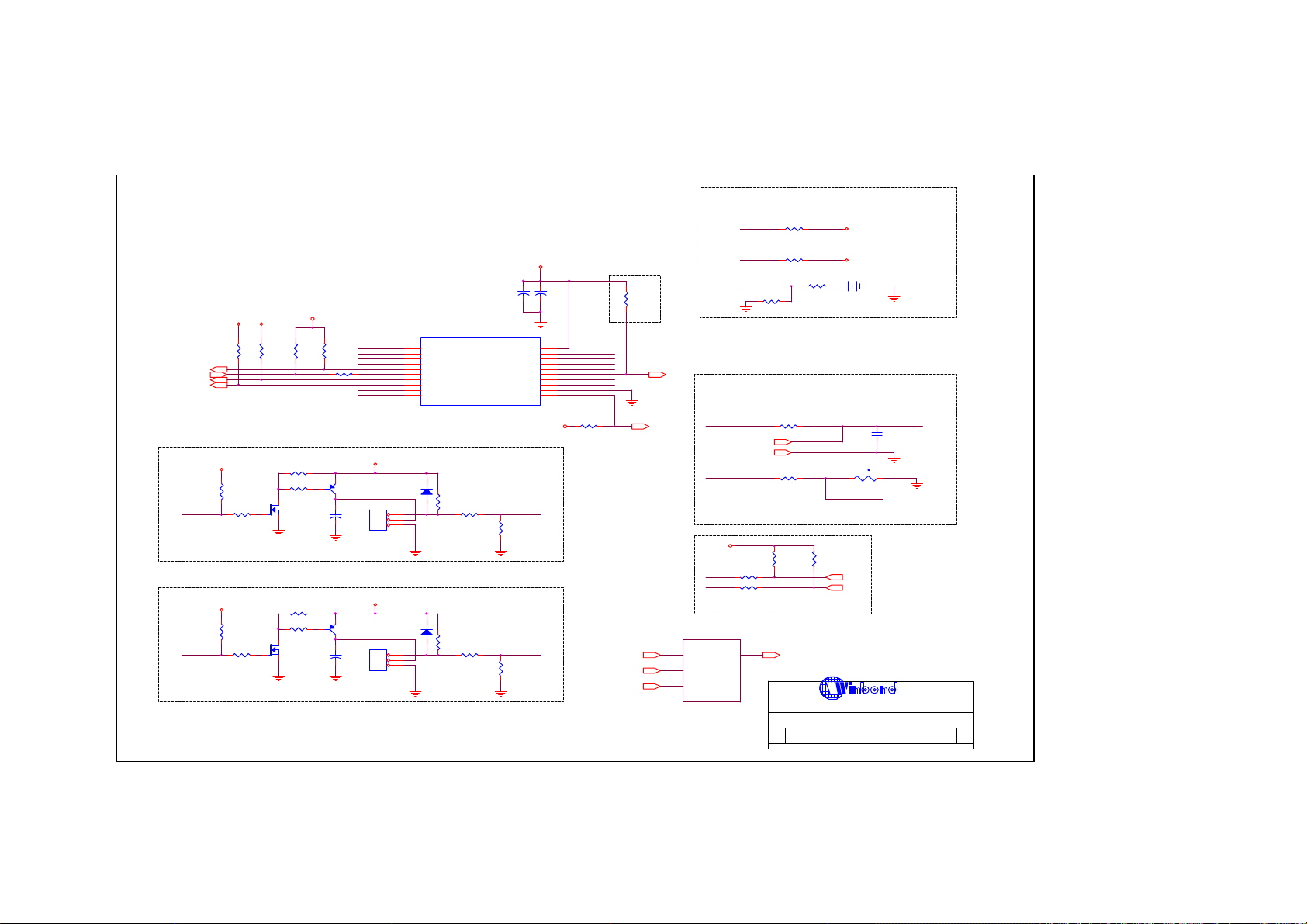
14. W83L784R SCHEMATICS
Rev.
0.1: Ignore.
0.2: W83L784R application circuit.
0.3: Change Pin5,Pin6,Pin11 to LOW Active.
Change Pin7 pull-up to 3VSB.
0.4: D1,D2,R9,R15 can be removed.
Change R1 to 0 Ohm. Add R27,R28,R29,R30(Reserved).
(Refer Application Notice 1)
0.5: Add a pull-up resistor R31.
R12 4.7K
R11
Q4
MOSFET N
R18 4.7K
R17
Q3
MOSFET N
VCC
R27
R28
FANIN1
10K
1K
1K
FANIN2 VT1/PII1
10K
PWMOUT1 VT2/PII2
PWMOUT2 VREF
R30
10K
SMI# +3.3VIN
OVT# VBAT
SCL
SDA
Fan5VCC
Q1
3906
C3
47u
C5
47u
JP1
Signal
+
Power
GND
HEADER 3
Fan5VCC
Q2
3906
JP2
Signal
+
Power
GND
HEADER 3
FANFAULT#
eg:
TO PIIX4
PWR_DN#
EXTSMI#
THRM#
SMARTFAN1 Speed Control Circuit
Fan5VCC
PWMOUT1 FANIN1
PWMOUT1 is
open-drain default.
When 784 is power-down,
Fan5VCC should be turned off.
SMARTFAN2 Speed Control Circuit
Fan5VCC
PWMOUT2 FANIN2
PWMOUT2 is
open-drain default.
When 784 is power-down,
Fan5VCC should be turned off.
3VCC 3VSB
R6
4.7KR74.7K
R23
4.7K
R19 4.7K
R24
4.7K
R20 4.7K
VOLTAGE SENSORING CIRCUIT
R8 R
VCORE
10K
R1 R
VCC
C1
C2
CAP
CAP
10u
0.1u
U1
1
FANIN1/GPO1
2
FANIN2/GPO2
3
PWMOUT1
4
PWMOUT2
5
FANFAULT#/GPO3
6
PWR_DN#
7
SMI#
8
OVT#
9
SCL
10
SDA
W83L784R
D1
1N4148
3
2
1
1N4148
3
2
1
R10
4.7K
D2
R16
4.7K
BATFAULT#/GPO4
R21 2K
R22 2K
CPUT1/PII1
CPUT2/PII2
VIN2(+3.3VIN)
VIN3(VBAT)
R9
10K
R15
10K
RESET#
20
VCC
19
18
17
VREF
16
VIN1
15
14
13
12
GND
11
VCC
Pull-up
R31
R
10K
VCORE
R29
10K
FANFAULT#
BATFAULT#
RESET#
BATFAULT#
uP
RESET#
+3.3VIN
0
VBAT
R26 R
R25
R
99K
TEMPERATURE SENSORING CIRCUIT
VREF VT1/PII1
VREF
Note:
1. CPUT1 is for CPU1 temperature and SMARTFAN 1
2. CPUT2 is for CPU2 temperature and SMARTFAN 2
3VCC
SDA
SCL
R14 R
30K 1%
PIID+
PIID-
R13 R
10K 1%
R4
R
4.7K
R3R0
R2
0
R
PWR_DN#
Title
W83L784R Application Circuit
Size Document Number Rev
784AP.SCH 0.5
B
Date: Sheet of
232K
R5
R
4.7K
WINBOND ELECTRONICS CORP.
RT1
THERMISTOR
VT2/PII2
SMDAT
SMCLK
CPU_VCORE
3VCC
BT1
BATTERY
DC 10V
C4
CAP
3300p
10K 1%
T
1 1Thursday, September 09, 1999
 Loading...