

Page 1

W83787IF
WINBOND I/O WITH SERIAL-INFRARED SUPPORT
PRELIMINARY
GENERAL DESCRIPTION
The W83787IF is a derivative product of W83787F with one of UARTs support HPSIR and ASKIR.
The W83787IF integrates a disk drive adapter ,two 16550 compatible UARTs, and one parallel port
with EPP mode, ECP mode, and joystick mode.
The disk drive adapter functions of the W83787IF is sames as W83787F which including a floppy
disk drive controller compatible with the industry standard 765, data separator, write precompensation circuit, decode logic, data rate selection, clock generator, drive interface control logic,
and interrupt and DMA logic. The wide range of functions integrated onto the W83787IF greatly
reduces the number of components required for interfacing with floppy disk drives. The W83787IF
supports four 360K, 720K, 1.2M, 1.44M disk drives and data transfer rates of 250Kb/S, 300Kb/S,
500Kb/S.
There are two high-speed serial communication ports (UARTs) on the W83787IF, one of them
support serial infrared communication. The UARTs include 16-byte send/receive FIFOs, a
programmable baud rate generator, complete modem control capability, and a processor interrupt
system.
The W83787IF supports three optional PC-compatible printer ports: 378h, 278h and 3BCh. Additional
bi-directional I/O capability is available by hardware control or software programming. The parallel
port also supports the Enhanced Parallel Port (EPP) and Extended Capabilities Port (ECP).
The W83787IF supports two embedded hard disk drive (AT bus) interfaces and a game port with
decoded read/write output.
The W83787IF's Extension FDD Mode and Extension 2FDD Mode allow one or two external floppy
disk drives to be connected to the computer through the printer interface pins in notebook computer
applications.
The Extension Adapter Mode of the W83787IF allows pocket devices to be installed through the
printer interface pins in notebook computer applications according to a protocol set by Winbond, but
with upgraded performance.
The JOYSTICK mode allows a joystick to be connected to a parallel port with a signal switching
cable.
The configuration register supports address selection, mode selection, function enable/disable, and
power down function selection.
Publication ReleaseDate:Sep 1995
- 1 - Revision A1
Page 2

W83787IF
FEATURES
• 1.44MB Floppy Disk Controller
--- Support four 360K,720K,1.2M,1.44M floppy disk drives
--- Data Transfer Rate 250Kb/s,300Kb/s,500Kb/s
--- Single 24Mhz crystal input
--- FDD anti-virus function with software write protect and FDD write enable signal,
write data signal force inactive
• Serial Ports
--- Two high speed 16550 UART with 16 byte FIFO
--- Programmable baud rate generator
--- Modem Control Circuitry
--- Support IrDA(HPSIR) and Amplitude Shift Keyed IR(ASKIR) Infrared communication
--- MIDI compatible
• Parallel Port
--- Support Standard Parallel Port(SPP),Enhanced Parallel Port(EPP),
Enhanced Capability Port(ECP)
--- Joystick mode supports joystick through parallel port
--- Extension FDD mode support disk drive B through parallel port
--- Extension Adapter Mode support pocket devices through parallel port
--- Extension 2FDD mode support disk drive A and B through parallel port
--- Compatible with IBM Parallel Port
--- Support parallel port with bi-directional lines
• IDE Interface
--- Support two embedded hard disk drives(IDE AT BUS)
• Game Port Supported
• Based on pinout of W83777/787F
• Two General Purpose I/O pins
• 100 PQFP
Publication Release Date:Sep 1995
- 2 - Revision A1
Page 3
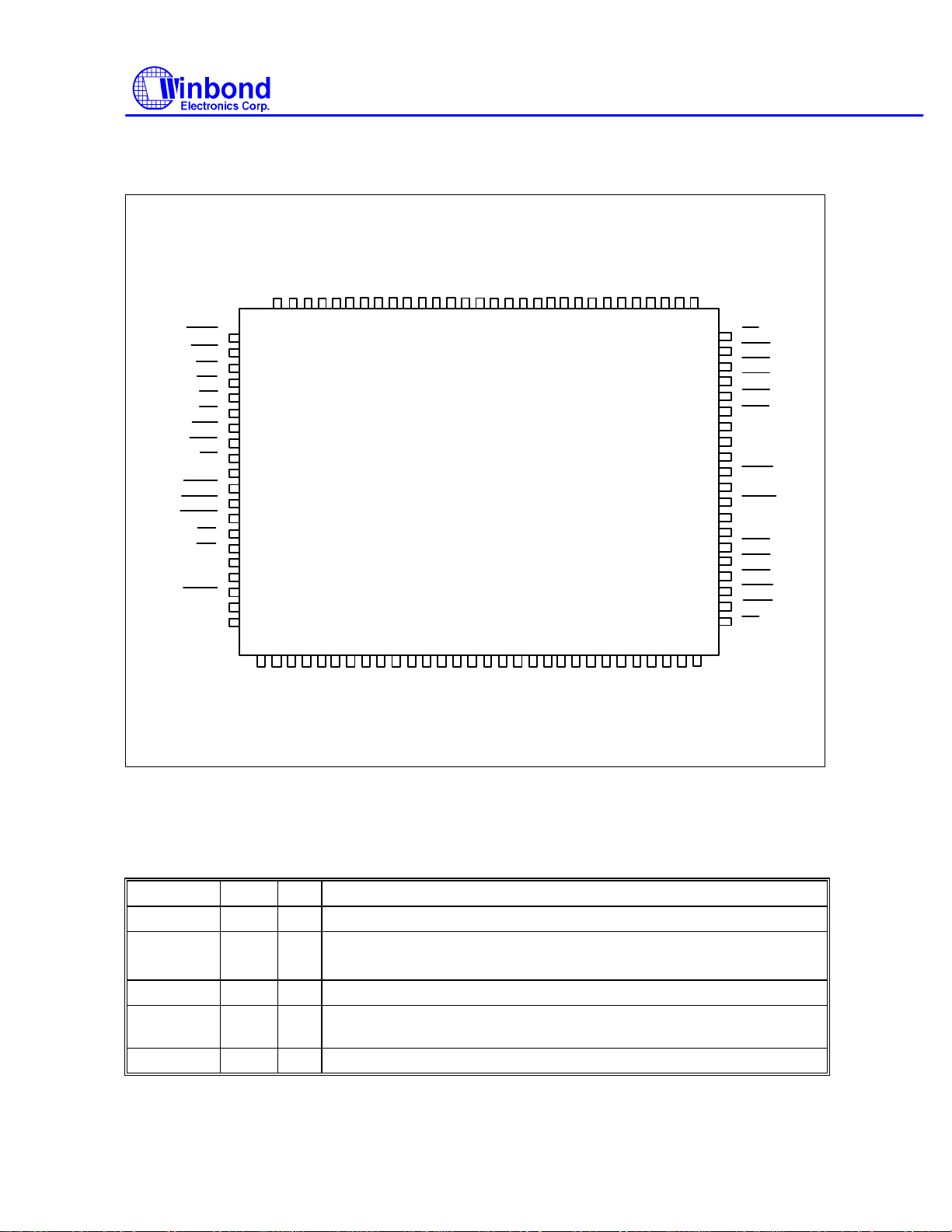
PIN CONFIGURATION
0
W
9
R
5
7
N
/
/
M
M
O
O
A
B
W83787IF
/
D
/
T
R
A
K
0
/
S
R
K
D
A
N
C
A
1
W
H
T
P
G
A
D
D
D
D
D
5
6
7
D
4
1
3D2
/
/
I
G
I
D
0
A
O
N
D
A
O
A8A7A
E
R
N
V
A
A
D
A2A
A
5
4
6
D
A
1
3
0
INDEX
STEP
DSA
DSB
WE
WD
RWC
HEAD
DIR
GND
DBENL
DBENH
IOCS16
CS0
CS1
IDED7
TC
DACK2
IRQ6
DRQ2
X X X X
80 79 78 77 76 75 74 73 72 71 70 69 68 67 66 65 64 63 62 61 60 59 58 57 56 55 54 53 52 51
X
81
X
82
X
83
X
84
X
85
X
86
X
87
X
88
X
89
X
90
X
91
X
92
X
93
X
94
95
X
X
96
X
97
X
98
X
99
X
100
1 2 3 4 5 6 7 8 9 10 11 12 13 14 15 16 1718 19 20 21 22 2324 25 26 27 28 29 30
/
P
P
P
R
D
D
D
E
C
R
B
S
I
Q
D
I
N
X
I
D
R
E
X
X
I
M
T
O
T
A
C
A
L
L
H
2
1
R
D
Y
X X X
X X X X X X X X XXX X X X XX X X X X X X X X X X X X
P
P
D
0
P
P
P
D
D
D
D
1
4
2
3
X X X X
P
P
V
P
D
D
D
D
6
D
XX X X X X
X X X X
X
/
/
/
/
/
S
P
T
R
B
T
O
E
I
S
A
I
R
L
F
N
Q
D
I
I
7
T
P
B
G
/
E
U
N
A
S
D
C
Y
K
X
RIB
50
X
DCDB
49
X
DSRB
48
X
CTSB
47
X
46
DTRB
X
45
RTSB
X
44
IRQ3
X
SOUTB
43
X
42
SINB
X
41
GMRD
X
40
GND
X
39
GMWR
X
38
SOUTA
X
IRQ4
37
X
36
RTSA
X
35
DTRA
X
34
CTSA
X
33
DSRA
X
32
DCDA
X
31
RIA
X
/
S
S
E
L
I
R
C
N
R
T
A
1.0 PIN DESCRIPTION
Note I: Input pin, O: Output pin, I/O: Bi-directional pin, OD: Open Drain pin.
1.1 Host Interface
SYMBOL PIN I/O FUNCTION
D0-D7 66-73 I/O System data bus bits 0-7
A0-A9 51-55
57-61
A10 75 I In ECP Mode, this pin is the A10 address input.
IOCHRDY 5 OD In EPP Mode, this pin is the IO Channel Ready output to extend the
MR 6 I Master Reset. Active high. MR is low during normal operations.
I System address bus bits 0-9
host read/write cycle.
Publication Release Date:Sep 1995
- 3 - Revision A1
Page 4
W83787IF
IOR
IOW
DACK
2
PRTOE
PDACKX
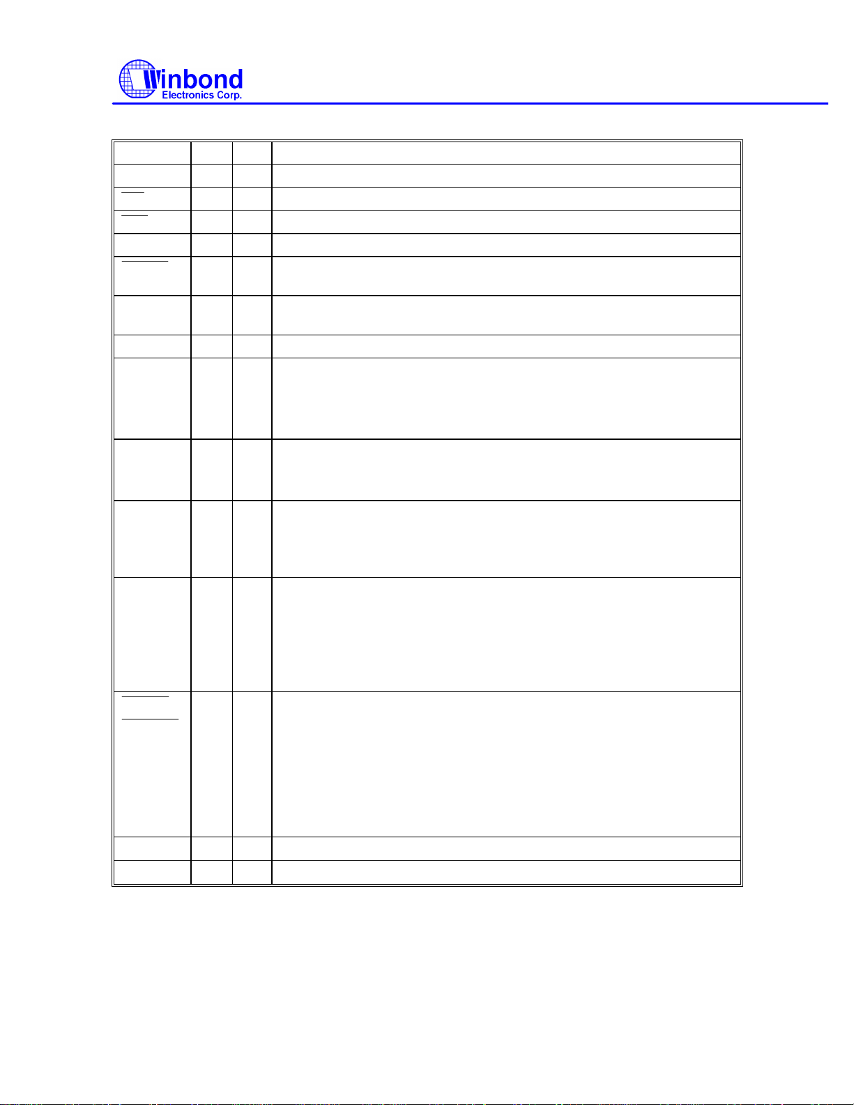
Host Interface, continued
SYMBOL PIN I/O FUNCTION
AEN 62 I
63 I
64 I
DRQ2 100 O
98 I
TC 97 I
IRQ6 99 O
IRQ4 37 O Interrupt request generated by UART A or UART B when their addresses
IRQ3 44 O
IRQ7 23 O
PDRQX
HPRTM1
XTAL1 7 I
XTAL2 8 O
4 I/O In Extension Adapter mode this pin is a DMA Request generated by
18 I In printer mode, this pin is for data direction control. When it is set to low,
System address bus enable
CPU I/O read signal
CPU I/O write signal
When DRQ2 = 1, a DMA request is being made by the FDC
DMA Acknowledge. When this pin is active, a DMA cycle is underway
and the controller is executing a DMA transfer.
Terminal Count. When active, this pin indicates termination of a DMA
transfer.
Interrupt request generated by FDC
are COM1 or COM3.
This interrupt request can be tri-stated by setting bit 3 of HCR low.
This signal is at high impedance after each reset operation.
Interrupt request generated by UART A or UART B when their addresses
are COM2 or COM4.
Same as IRQ4
When IRQ7 = 1 and interrupt request is being made by the printer, this
pin is pulled high internally.
In EPP or ECP mode, IRQ7 is pulsed low, then released to allow sharing
of interrupts.
Extension Adapter. This request is output directly from XDRQ.
In ECP mode, this pin is the parallel port DMA Request output.
During power-on reset, this pin is pulled down internally and is defined as
HPRTM1, which is used for selecting the mode of the parallel port (see
Table 1-1).
the parallel port functions as an output port. When it is set to high, the
direction of the data bus is controlled by Bit 5 (DIR) of the printer control
register and Bit 7 (PRTBEN) of CR3. This pin is pulled up internally.
In Extension Adapter mode, this pin is the DMA acknowledge for the
Extension Adapter. When this pin is active, a DMA cycle is underway
and the controller is executing a DMA transfer.
In ECP mode, this pin is the parallel port DMA Acknowledge input.
24Mhz XTAL/Oscillator/Clock input
XTAL output
Publication Release Date:Sep 1995
- 4 - Revision A1
Page 5
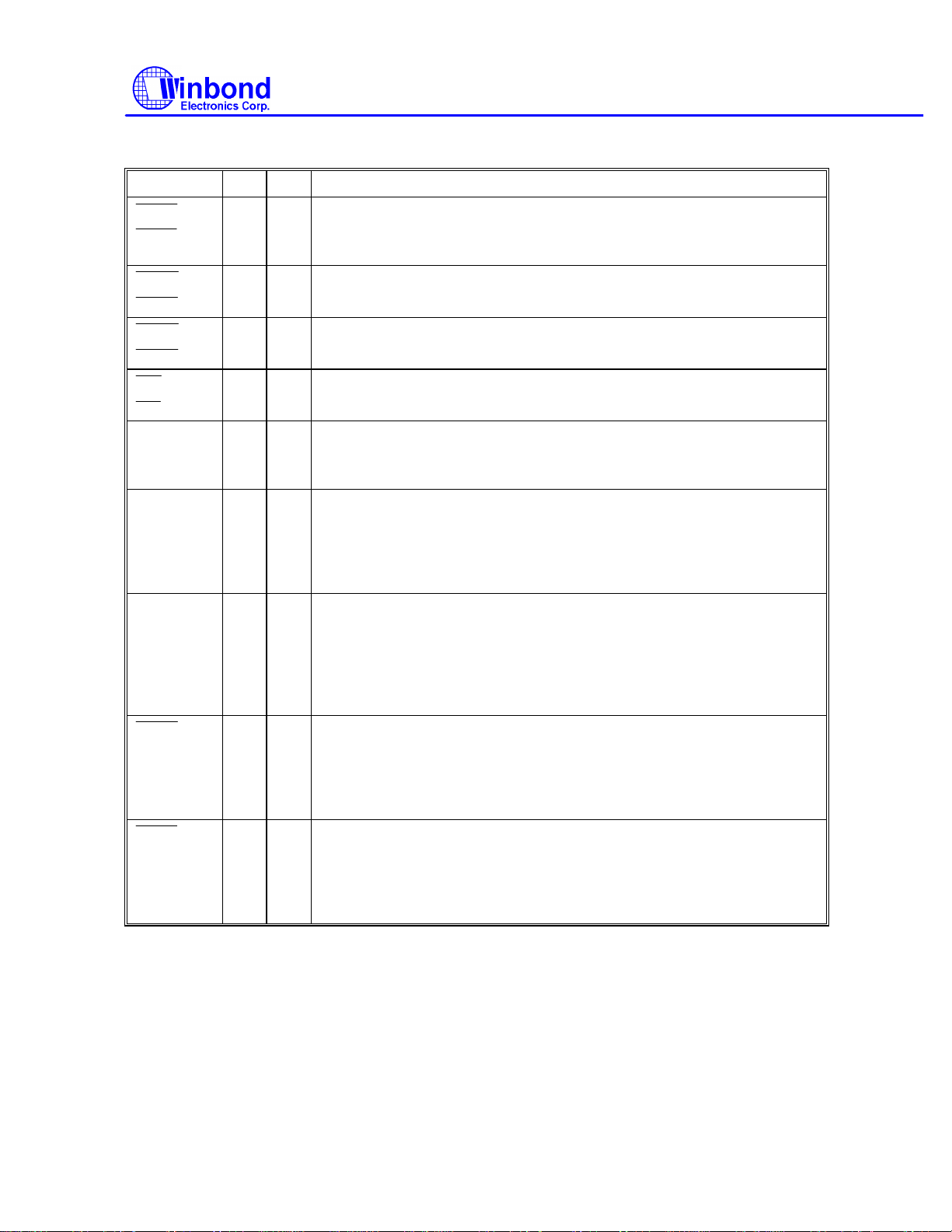
1.2 Serial Port Interface
CTSA
CTSB
DSRA
DSRB
DCDA
DCDB
RIA
RIB
DTRA
DTRB
SYMBOL PIN I/O FUNCTION
34
47
33
48
I Clear To Send is the modem control input.
The function of these pins can be tested by reading Bit 4 of the
handshake status register.
I Data Set Ready. An active low indicates the modem or data set is ready
to establish a communication link and transfer data to the UART.
W83787IF
SINA
SINB
IRRX1
SOUTA
HURAS1
SOUTB
HURBS1
IRTX1
HPRTAS0
HURAS0
32
49
31
50
30
42
38 I/O UART A Serial Output. Used to transmit serial data out to the
43 I/OOUART B Serial Output. Used to transmit serial data out to the
35 I/O UART A Data Terminal Ready. An active low informs the modem or
46 I/O UART B Data Terminal Ready. An active low informs the modem or
I Data Carrier Detect. An active low indicates the modem or data set has
detected a data carrier.
I Ring Indicator. An active low indicates that a ring signal is being
received by the modem or data set.
I Serial Input. Used to receive serial data from the communication link.
SINB can be programmed by CR0D register as input pin IRRX1 for
serial infrared communication
communication link.
During power-on reset, this pin is pulled up internally and is defined as
HURAS1, which is used for selecting the I/O address of the UART A.
(See Table 1-2.)
communication link. SOUTB can be programmed by CR0D register as
output pin IRTX1 for serial infrared communication.
During power-on reset, this pin is pulled up internally and is defined as
HURBS1, which is used for selecting the I/O address of UARTB. (See
Table 1-2.)
data set that the controller is ready to communicate.
During power-on reset, this pin is pulled down internally and is defined
as HPRTAS0. It is used for selecting the address of the parallel port.
(See Table 1-3.)
data set that controller is ready to communicate.
During power-on reset, this pin is pulled down internally and is defined
as HURAS0. It is used for setting the I/O address of UART A. (See
Table 1-2.)
Publication Release Date:Sep 1995
- 5 - Revision A1
Page 6
W83787IF
RTSA
RTSB
GMRD
GMWR
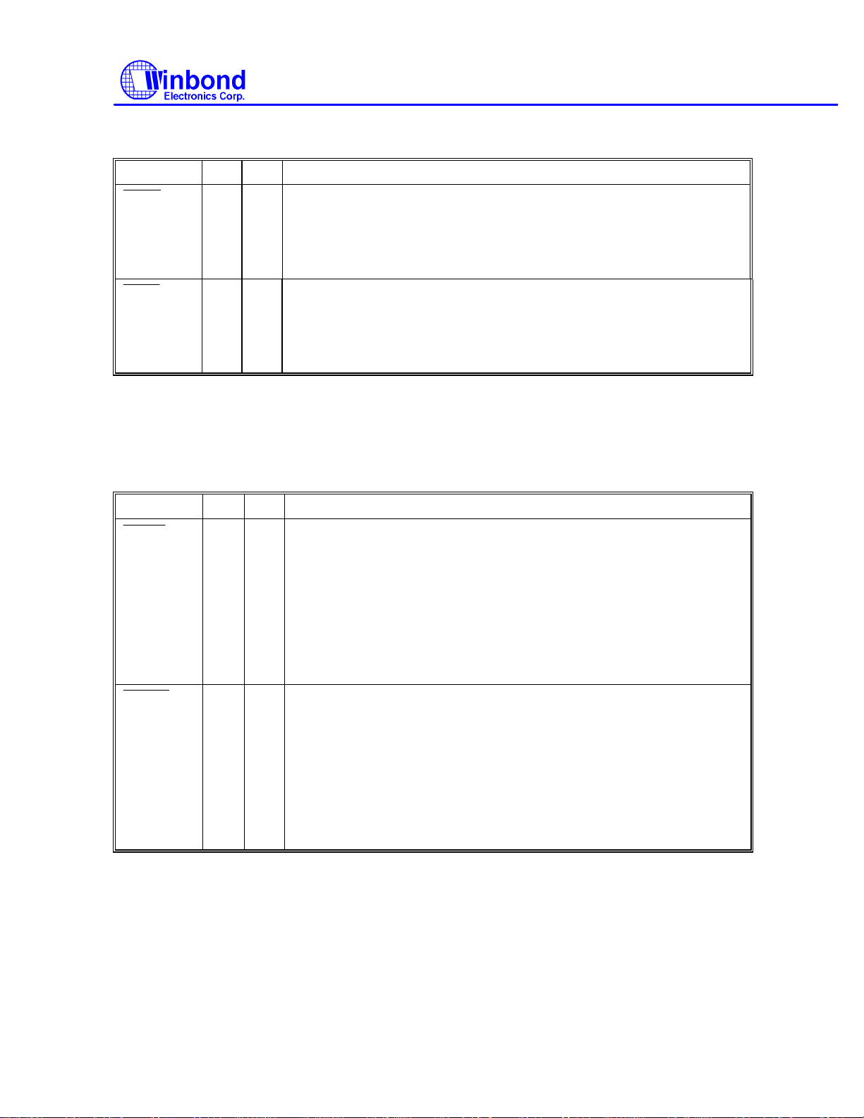
Serial Port Interface, continued
SYMBOL PIN I/O FUNCTION
36 I/O UART A Request To Send. An active low informs the modem or data
HPRTAS1
45 I/O UART B Request To Send. An active low informs the modem or data
HURBS0
1.3 Game Port/Power Down Interface
Bit 4 of CR3 (GMODS0) determines whether the game port is in Adapter mode or Portable mode
(default is Adapter mode).
Game I/O port address is 201h.
set that the controller is ready to send data.
During power-on reset, this pin is pulled up internally and is defined as
HPRTAS1. It is used for setting the address of the parallel port. (See
Table 1-3.)
set that the controller is ready to send data.
During power-on reset, this pin is pulled down internally and is defined
as HURBS0. It is used for setting the I/O address of UART B. (See
Table 1-2.)
SYMBOL PIN I/O FUNCTION
41 O
PFDCEN
HEFERE
39 O
PEXTEN
HPRTM0
Adapter mode: Game port read control signal.
Portable mode: When parallel port is selected as Extension
O
FDD/Extension 2FDD mode, this pin will be active. The active state is
I
dependent on bit 7 of CRA (PFDCACT), and default is low active.
During power-on reset, this pin is pulled up internally and is defined as
HEFERE for determining whether Extended Function Enable Register
enable value is 88h or 89h. If the HEFERE= H (default) at power-on
reset, then EFER enable value is 89h. If HEFERE = L at power-on
reset, the enable value is 88h.
Adapter mode: Game port write control signal.
Portable mode: When a particular extended mode is selected for the
O
parallel port, this pin will be active. The extended modes include
I
Extension Adapter mode, EPP mode, ECP mode, and ECP/EPP mode,
which are selected using bit 3 - bit 0 of CRA. The active state is
dependent on bit 6 of CRA (PEXTACT); the default is low active.
During power-on reset, this pin is pulled down internally and is defined
as HPRTM0. It is used to determine the mode of the parallel port. (See
Table 1-1.)
Publication Release Date:Sep 1995
- 6 - Revision A1
Page 7
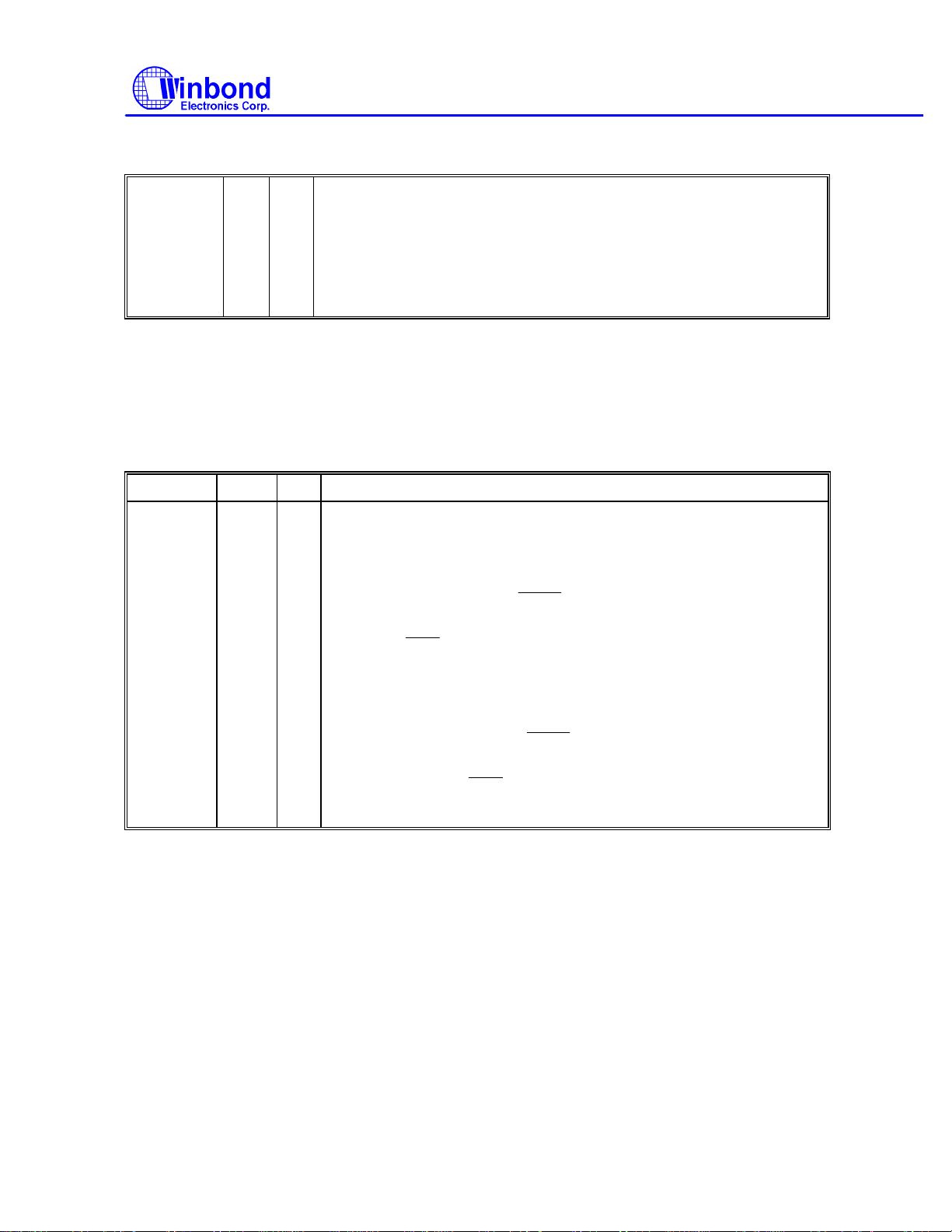
Game Port/Power Down Interface, continued
MOB
2
MOB
MOB
2
MOB
W83787IF
PDCIN
IRRX2
3 I
This input pin controls the chip power down. When this pin is active, the
clock supply to the chip will be inhibited and the output pins will be tri-
I
stated as defined in CR4 and CR6. The PDCIN is pulled down
internally. Its active state is defined by bit 4 of CRA (PDCHACT).
Default is high active.
PDCIN can be programmed by CR0D register as input pin IRRX2 for
serial infrared communication.
1.4 Multi-Mode Parallel Port
The following pins have eight functions, which are controlled by bits PRTMOD0, PRTMOD1, and
PRTMOD2 of CR0 and CR9 (refer to section 6.0, Extended Functions).
SYMBOL PIN I/O FUNCTION
BUSY
24 I
PRINTER MODE: BUSY
An active high input indicates that the printer is not ready to receive
data. This pin is pulled high internally. Refer to the description of the
parallel port for the definition of this pin in ECP and EPP mode.
EXTENSION FDD MODE:
OD
This pin is for Extension FDD B; the function of this pin is the same as
that of the
EXTENSION ADAPTER MODE: XIRQ
I
This pin is an interrupt request generated by the Extension Adapter
and is an active high input.
pin.
EXTENSION 2FDD MODE:
OD
This pin is for Extension FDD A and B; the function of this pin is the
same as that of the
JOYSTICK MODE: NC pin.
_
- 7 - Revision A1
pin.
Publication Release Date:Sep 1995
Page 8
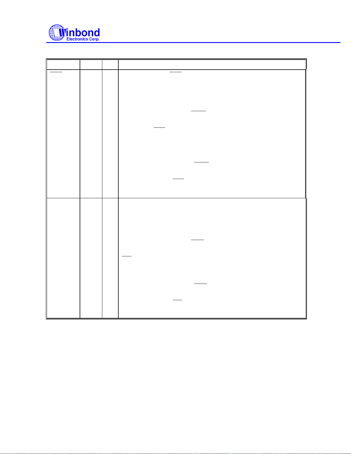
Multi-Mode Parallel Port, continued
ACK
ACK
DSB
2
DSB
DSB
2
DSB
WD
2
WD
WD
2
SYMBOL PIN I/O FUNCTION
W83787IF
PE
26 I
OD
OD
27 I
PRINTER MODE:
An active low input on this pin indicates that the printer has received
data and is ready to accept more data. This pin is pulled high
internally. Refer to the description of the parallel port for the definition
of this pin in ECP and EPP mode.
EXTENSION FDD MODE:
This pin is for the Extension FDD B; its functions are the same as
those of the
EXTENSION ADAPTER MODE: XDRQ
I
pin.
DMA request generated by the Extension Adapter. An active high
input.
EXTENSION 2FDD MODE:
This pin is for Extension FDD A and B; this function of this pin is the
same as that of the
JOYSTICK MODE: NC pin.
_
pin.
PRINTER MODE: PE
An active high input on this pin indicates that the printer has detected
the end of the paper. This pin is pulled high internally.
Refer to the description of the parallel port for the definition of this pin
in ECP and EPP mode.
EXTENSION FDD MODE:
OD
This pin is for Extension FDD B; its function is the same as that of the
pin.
EXTENSION ADAPTER MODE: XA0
O
This pin is system address A0 for the Extension Adapter.
EXTENSION 2FDD MODE:
OD
This pin is for Extension FDD A and B; this function of this pin is the
same as that of the WD pin.
JOYSTICK MODE: NC pin.
_
Publication Release Date:Sep 1995
- 8 - Revision A1
Page 9
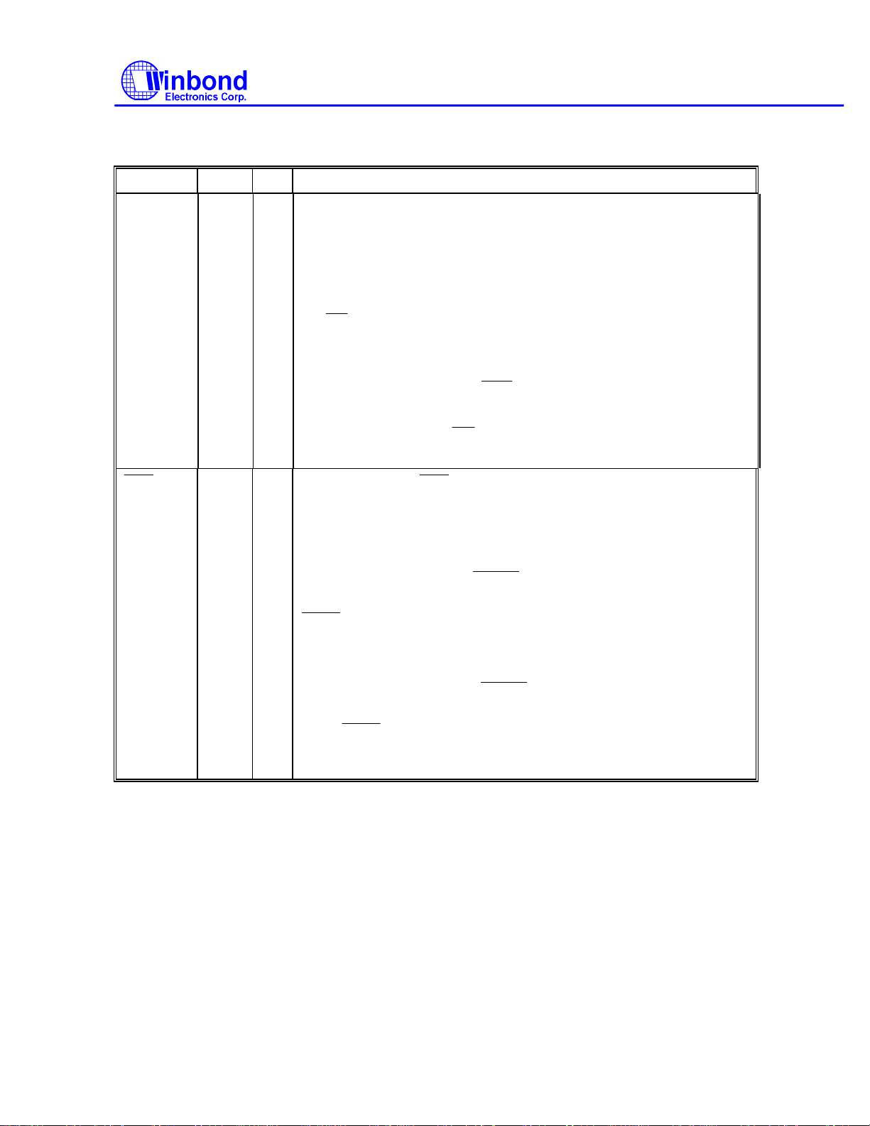
Multi-Mode Parallel Port, continued
WE
2
ERR
ERR
HEAD
2
HEAD
HEAD
2
HEAD
SYMBOL PIN I/O FUNCTION
SLCT
28 I
29 I
PRINTER MODE: SLCT
An active high input on this pin indicates that the printer is selected.
This pin is pulled high internally. Refer to the description of the parallel
port for the definition of this pin in ECP and EPP mode.
OD
EXTENSION FDD MODE: WE2
This pin is for Extension FDD B; its functions are the same as those of
the WE pin.
EXTENSION ADAPTER MODE: XA1
O
This pin is system address A1 for the Extension Adapter.
EXTENSION 2FDD MODE:
OD
This pin is for Extension FDD A and B; this function of this pin is
the same as that of the WE pin.
_
JOYSTICK MODE: NC pin.
PRINTER MODE:
An active low input on this pin indicates that the printer has
encountered an error condition. This pin is pulled high internally. Refer
to the description of the parallel port for the definition of this pin in
ECP and EPP mode.
W83787IF
EXTENSION FDD MODE:
OD
This pin is for Extension FDD B; its function is the same as that of the
pin.
EXTENSION ADAPTER MODE: XA2
O
This pin is system address A2 for the Extension Adapter.
EXTENSION 2FDD MODE:
OD
This pin is for Extension FDD A and B; its function is the same as that
of the
JOYSTICK MODE: NC pin.
_
pin.
Publication Release Date:Sep 1995
- 9 - Revision A1
Page 10
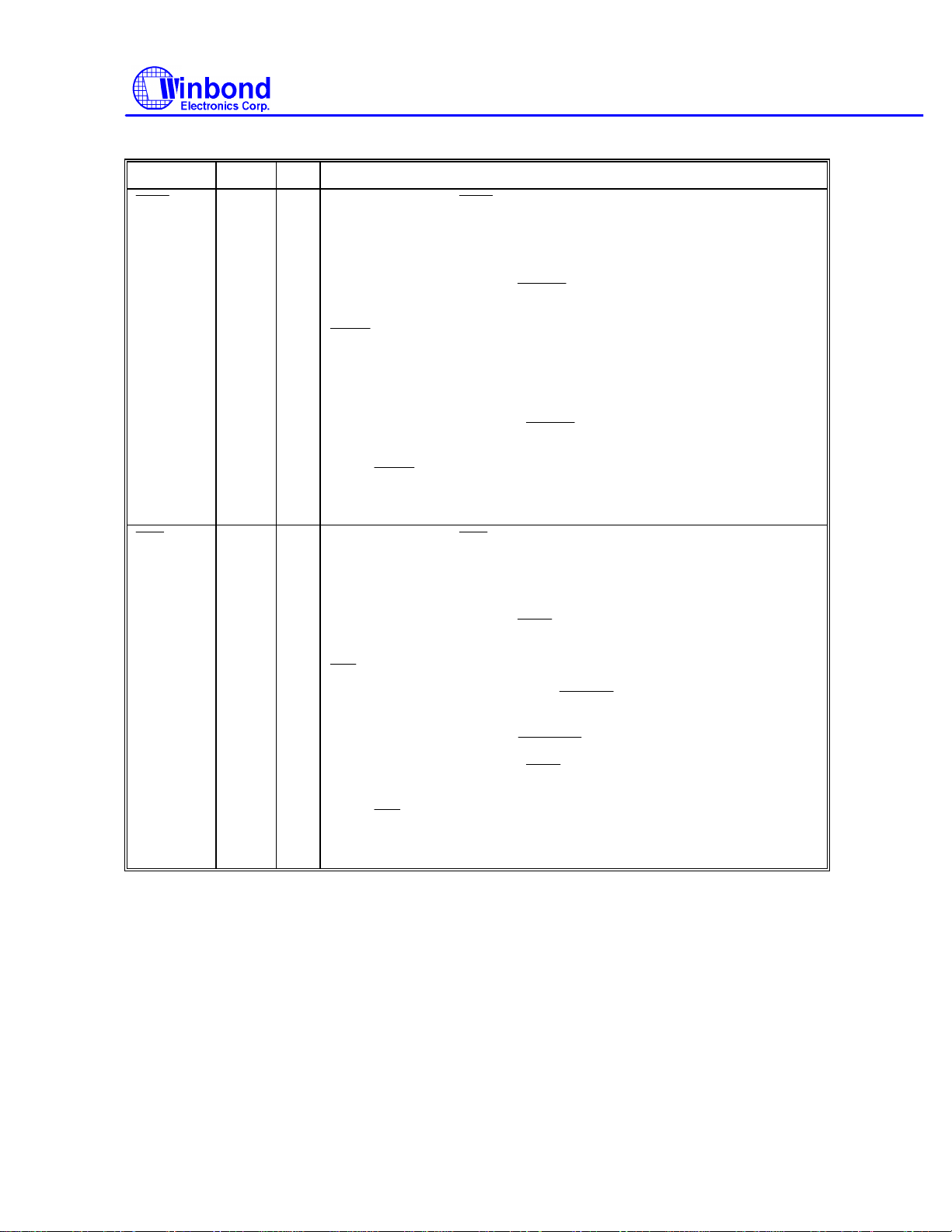
Multi-Mode Parallel Port, continued
SLIN
SLIN
STEP
2
STEP
STEP
2
STEP
INIT
INIT
DIR
2
DIR
XDACK
PDACKX
DIR
2
DIR
SYMBOL PIN I/O FUNCTION
W83787IF
22 OD
OD
O
OD
O
21 OD
OD
PRINTER MODE:
Output line for detection of printer selection. This pin is pulled high
internally. Refer to the description of the parallel port for the definition
of this pin in ECP and EPP mode.
EXTENSION FDD MODE:
This pin is for Extension FDD B; its function is the same as that of the
pin.
EXTENSION ADAPTER MODE: XTC
This pin is the DMA terminal count for the Extension Adapter. The
count is sent by TC directly.
EXTENSION 2FDD MODE:
This pin is for Extension FDD A and B; its function is the same as that
of the
JOYSTICK MODE: VDD for joystick.
PRINTER MODE:
Output line for the printer initialization. This pin is pulled high
internally. Refer to the description of the parallel port for the definition
of this pin in ECP and EPP mode.
EXTENSION FDD MODE:
This pin is for Extension FDD B; its function is the same as that of the
pin.
pin .
EXTENSION ADAPTER MODE:
O
This pin is the DMA acknowledge output for the Extension Adapter; the
output is sent directly from
EXTENSION 2FDD MODE:
OD
This pin is for Extension FDD A and B; its function is the same as that
of the
JOYSTICK MODE: VDD for joystick.
O
pin.
- 10 - Revision A1
.
Publication Release Date:Sep 1995
Page 11
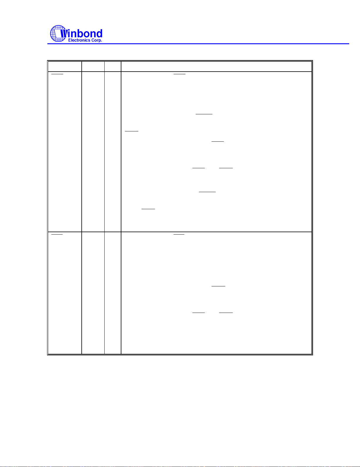
Multi-Mode Parallel Port, continued
AFD
AFD
RWC
2
RWC
XRD
XRD
XWR
RWC
2
RWC
STB
STB
XWR
XRD
XWR
SYMBOL PIN I/O FUNCTION
W83787IF
20 OD
OD
O
OD
O
19 OD
-
PRINTER MODE:
An active low output from this pin causes the printer to auto feed a line
after a line is printed. This pin is pulled high internally. Refer to the
description of the parallel port for the definition of this pin in ECP and
EPP mode.
EXTENSION FDD MODE:
This pin is for Extension FDD B; its function is the same as that of the
pin.
EXTENSION ADAPTER MODE:
This pin is the I/O read command for the Extension Adapter.
When the Extension Adapter base address is written to the Extension
Adapter address register,
that the command register on the Extension Adapter can latch the
same base address.
EXTENSION 2FDD MODE:
This pin is for Extension FDD A and B; its function is the same as that
of the
JOYSTICK MODE: VDD for joystick.
PRINTER MODE:
An active low output is used to latch the parallel data into the printer.
This pin is pulled high internally. Refer to the description of the parallel
port for the definition of this pin in ECP and EPP mode.
EXTENSION FDD MODE:
This pin is a tri-state output.
pin.
and
go low simultaneously so
EXTENSION ADAPTER MODE:
O
This pin is the I/O write command for the Extension Adapter.
When the Extension Adapter base address is written to the Extension
Adapter address register,
that the command register on the Extension Adapter can latch the
same base address.
EXTENSION 2FDD MODE: This pin is a tri-state output.
JOYSTICK MODE: VDD for joystick.
O
- 11 - Revision A1
and
go low simultaneously so
Publication Release Date:Sep 1995
Page 12
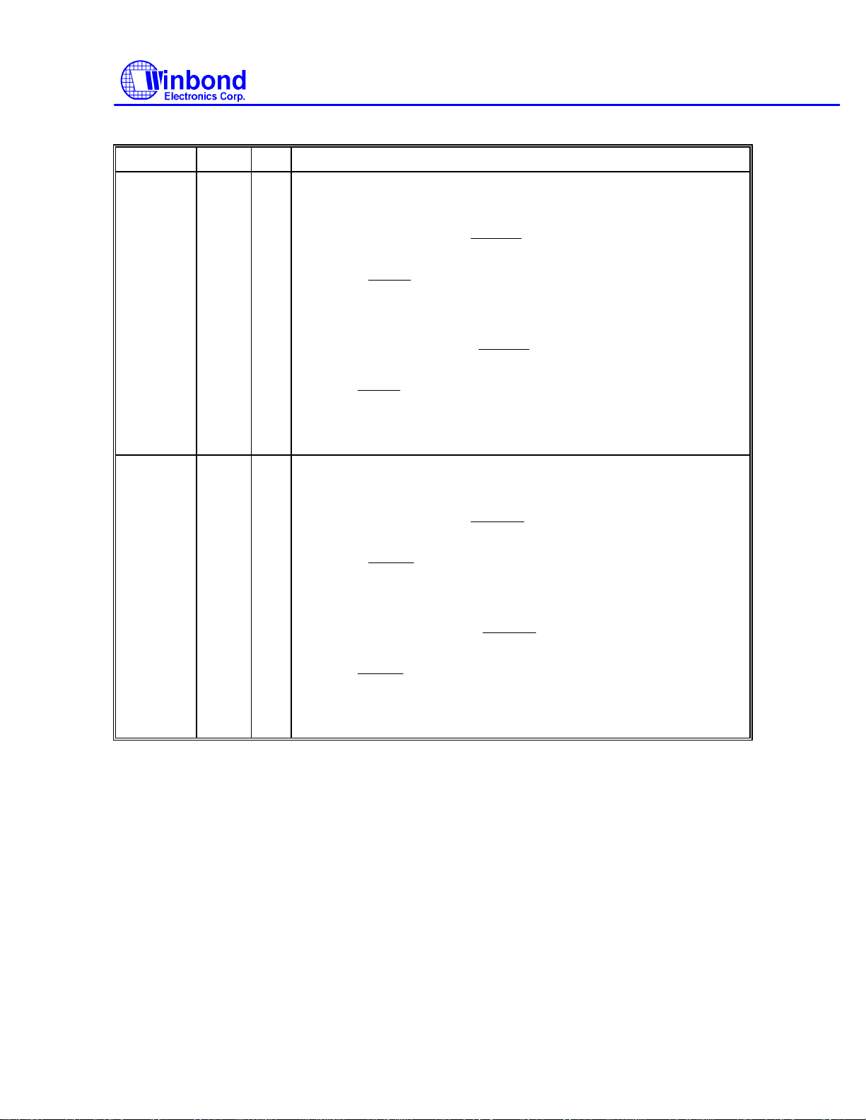
Multi-Mode Parallel Port, continued
INDEX
2
INDEX
INDEX
2
INDEX
TRAK
02
TRAK
0
TRAK
02
TRAK
0
SYMBOL PIN I/O FUNCTION
W83787IF
PD0
PD1
9 I/O
I
I/O
I
I/O
10 I/O
I
I/O
PRINTER MODE: PD0
Parallel port data bus bit 0. Refer to the description of the parallel port
for the definition of this pin in ECP and EPP mode.
EXTENSION FDD MODE:
This pin is for Extension FDD B; the function of this pin is the same as
that of the
EXTENSION ADAPTER MODE: XD0
This pin is system data bus D0 for the Extension Adapter.
EXTENSION 2FDD MODE:
This pin is for Extension FDD A and B; this function of this pin is the
same as
JOYSTICK MODE: JP0
This pin is the paddle 0 input for joystick.
PRINTER MODE: PD1
Parallel port data bus bit 1. Refer to the description of the parallel port
for the definition of this pin in ECP and EPP mode.
EXTENSION FDD MODE:
This pin is for Extension FDD B; the function of this pin is the same as
that of the
EXTENSION ADAPTER MODE: XD1
This pin is system data bus D1 for the Extension Adapter.
pin. This pin is pulled high internally.
pin. This pin is pulled high internally.
pin. This pin is pulled high internally.
EXTENSION. 2FDD MODE:
I
This pin is for Extension FDD A and B; this function of this pin is the
same as
JOYSTICK MODE: JP1
I/O
This pin is the paddle 1 input for joystick.
pin. This pin is pulled high internally.
Publication Release Date:Sep 1995
- 12 - Revision A1
Page 13
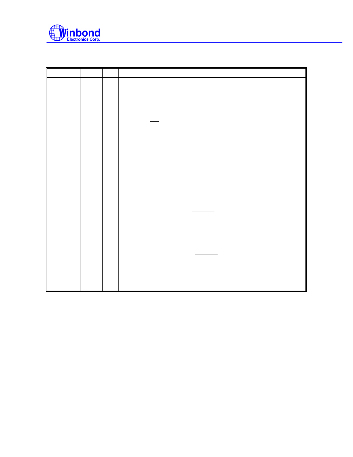
Multi-Mode Parallel Port, continued
WP
2
WP
2
RDATA
2
RDATA
RDATA
2
RDATA
SYMBOL PIN I/O FUNCTION
PD2
PD3 12 I/O
11 I/O
PRINTER MODE: PD2
Parallel port data bus bit 2. Refer to the description of the parallel port
for the definition of this pin in ECP and EPP mode.
EXTENSION FDD MODE:
I
This pin is for Extension FDD B; the function of this pin is the same as
that of the WP pin. This pin is pulled high internally.
EXTENSION ADAPTER MODE: XD2
I/O
This pin is system data bus D2 for the Extension Adapter.
EXTENSION. 2FDD MODE:
I
This pin is for Extension FDD A and B; this function of this pin is the
same as that of the WP pin. This pin is pulled high internally.
JOYSTICK MODE: NC pin
PRINTER MODE: PD3
Parallel port data bus bit 3. Refer to the description of the parallel port
for the definition of this pin in ECP and EPP mode.
I
EXTENSION FDD MODE:
Motor on B for Extension FDD B; the function of this pin is the same
as that of the
EXTENSION ADAPTER MODE: XD3
I/O
This pin is system data bus D3 for the Extension Adapter.
EXTENSION 2FDD MODE:
I
This pin is for Extension FDD A and B; this function of this pin is the
same as that of the
JOYSTICK MODE: NC pin
-
pin. This pin is pulled high internally.
pin. This pin is pulled high internally.
W83787IF
Publication Release Date:Sep 1995
- 13 - Revision A1
Page 14
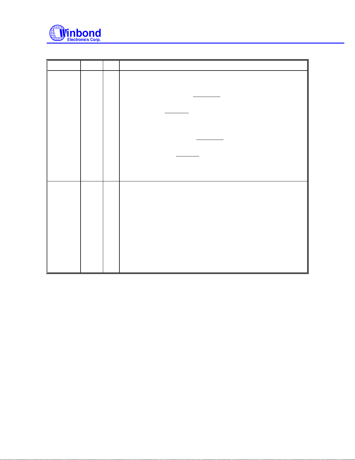
Multi-Mode Parallel Port, continued
DSKCHG
2
DSKCHG
DSKCHG
2
DSKCHG
SYMBOL PIN I/O FUNCTION
PD4 13 I/O
PD5 14 I/O
PRINTER MODE: PD4
Parallel port data bus bit 4. Refer to the description of the parallel port
for the definition of this pin in ECP and EPP mode.
I
EXTENSION FDD MODE:
Drive select B for Extension FDD B; the function of this pin is the
same as that of
EXTENSION ADAPTER MODE: XD4
I/O
This pin is system data bus D4 for the Extension Adapter.
EXTENSION 2FDD MODE:
I
This pin is for Extension FDD A and B; this function of this pin is the
same as that of the
JOYSTICK MODE: JB0
I
This pin is the button 0 input for the joystick.
PRINTER MODE: PD5
Parallel port data bus bit 5. Refer to the description of the parallel port
for the definition of this pin in ECP and EPP mode.
-
EXTENSION FDD MODE:
This pin is a tri-state output.
I/O
EXTENSION ADAPTER MODE: XD5
This pin is system data bus D5 for the Extension Adapter
-
EXTENSION 2FDD MODE:
This pin is a tri-state output.
I
JOYSTICK MODE: JB1
This pin is the button 1 input for the joystick.
pin. This pin is pulled high internally.
pin. This pin is pulled high internally.
W83787IF
Publication Release Date:Sep 1995
- 14 - Revision A1
Page 15
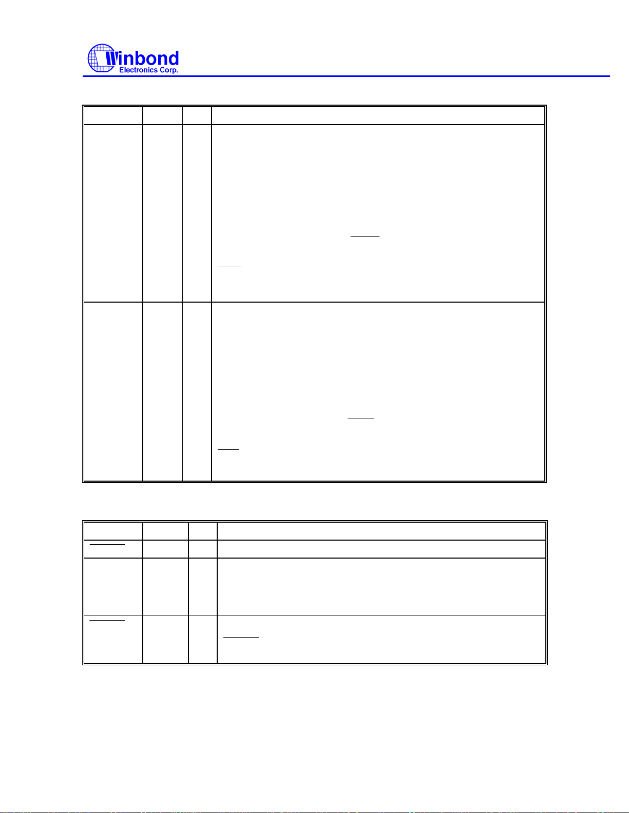
Multi-Mode Parallel Port, continued
MOA
2
MOA
DSA
2
DSA
IOCS
16
RESIDE
RESIDE
SYMBOL PIN I/O FUNCTION
W83787IF
PD6 16 I/O
-
I/O
OD
-
PD7 17 I/O
-
I/O
OD
-
PRINTER MODE: PD6
Parallel port data bus bit 6. Refer to the description of the parallel port
for the definition of this pin in ECP and EPP mode.
EXTENSION FDD MODE:
This pin is a tri-state output.
EXTENSION ADAPTER MODE: XD6
This pin is system data bus D6 for the Extension Adapter
EXTENSION. 2FDD MODE:
This pin is for Extension FDD A; its function is the same as that of the
pin.
JOYSTICK MODE: NC pin
PRINTER MODE: PD7
Parallel port data bus bit 7. Refer to the description of the parallel port
for the definition of this pin in ECP and EPP mode.
EXTENSION FDD MODE:
This pin is a tri-state output.
EXTENSION ADAPTER MODE: XD7
This pin is system data bus D7 for the Extension Adapter.
EXTENSION 2FDD MODE:
This pin is for Extension FDD A; its function is the same as that of the
pin.
JOYSTICK MODE: NC pin
1.5 IDE and FDC Interface
SYMBOL PIN I/O FUNCTION
93 I 16-bit I/O indication from IDE interface
IDED7
GIO1
IRRX3
96 I/O
1 OIReset signal for IDE, active low to initialize the IDE
IDE data bus bit 7
I/O
GIO1:General Purpose I/O pin 1.If pin #91 GIOSEL=1,this pin act as
GIO1.If GIOSEL=0,this pin act as IDED7.It can also be programmed
by CR0C register bit 2.
can be programmed by CR0D register as input pin IRRX3
for serial infrared communication.
- 15 - Revision A1
Publication Release Date:Sep 1995
Page 16

IDE and FDC Interface, continued
DBENL
IDBEN
DBENL
DBENL
IDBEN
IDBEN
DBENL
DBENH
DBENH
DBENH
DBENH
FDCEN
FDCEN
SYMBOL PIN I/O FUNCTION
W83787IF
GIOSEL
GIO0
URIRSEL
PDBDIR
IRTX2
91 O
92 O
I/O
2 I/O
During normal operations,
buffer of the IDE bus. When
O
addresses 1F0H - 1F7H (170H-177H) and 3F6-3F7H (376H-377H).
I
:IDE Data Bus Enable(Low Active). If I/O address 1F0~1F7H
and 2F7H is access, the pin will activate.
During power on reset,if GIOSEL=1,then this pin act as
GIOSEL=0,this pin act as
CR0C register bit 2.
GIOSEL:General Purpose I/O pin select at power on setting. (See
Table 1-4)
During normal operations,
buffer of the IDE bus.
When active,
I
(170H-177H).
GIO0:General Purpose I/O pin0. If pin #91 GIOSEL=1,this pin act as
GIO0.If GIOSEL=0,this pin act as nDBENH.It can also be
programmed by CR0C register bit 2.
URIRSEL:UART/IR Selection.During power on reset,if
URIRSEL=1,then UARTB act as UART function. If URIRSEL=0,then
UARTB act as IR function.
During normal operation, this pin (PDBDIR) is an output that
indicates the direction of the parallel port data bus. If bit 5 of CRA
(PDIRHISOP) is low, then PDBDIR = 0 means output/write, PDBDIR
O
= 1 means input/read (default). During power-on reset, this pin
(
4.7K resistor is recommend in order to pullup the pin at power on
reset to disable the FDC function.
When set to low, it enables the FDC port (default).
When set to high, it disables the FDC port.
PDBDIR can be programmed by CR0D register as output pin IRTX2
for serial infrared communication.
) is pulled down internally and is used to enable the FDC. A
selects I/O port address range 1F0-1F7H
is used to enable the low byte
is active, it accesses I/O
.It can also be programmed by
is used to enable the high byte
is active only when /IOCS16 is active.
.If
Publication Release Date:Sep 1995
- 16 - Revision A1
Page 17
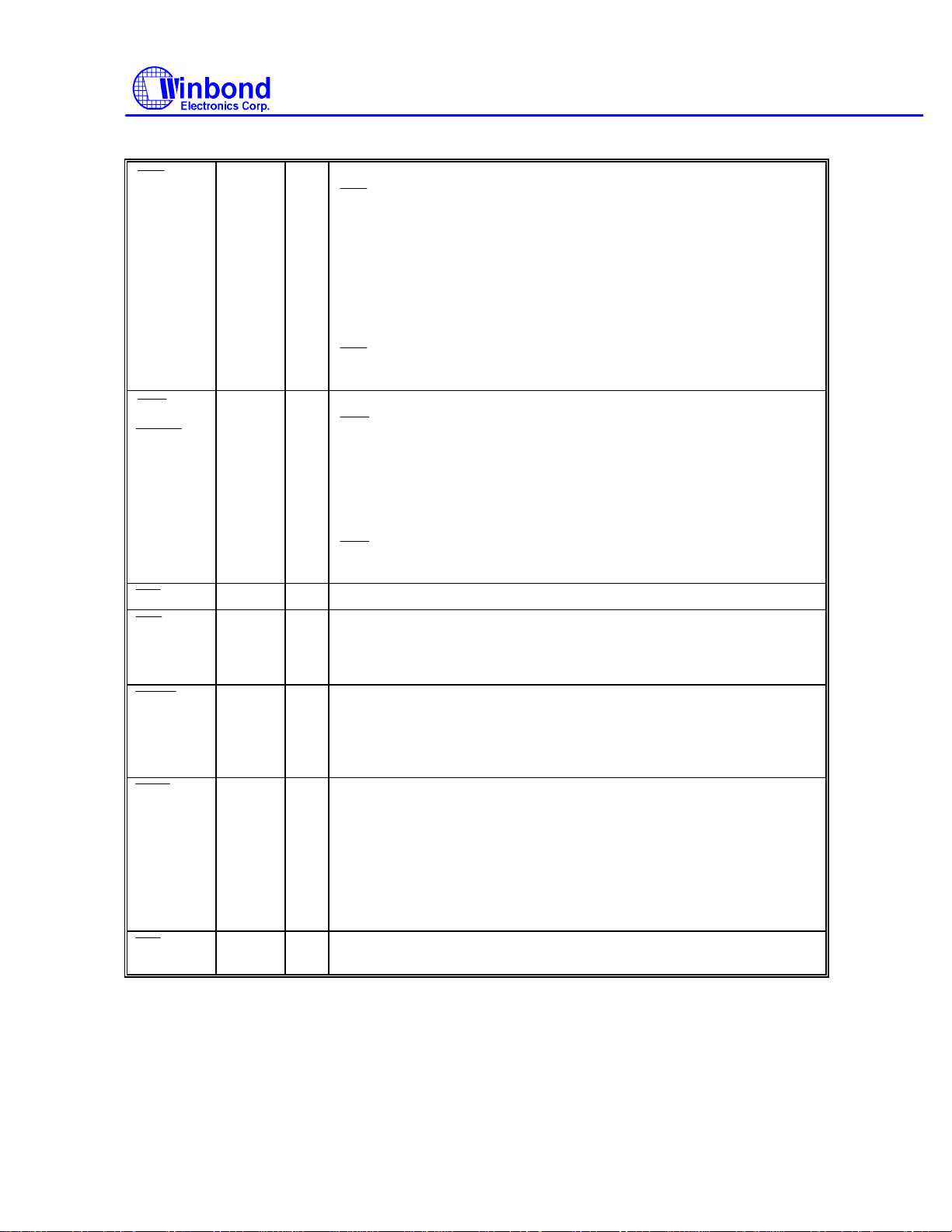
IDE and FDC Interface, continued
CS1
CS1
CS1
CS0
IDEEN
CS0
CS0
WE
DIR
HEAD
RWC
WD
W83787IF
HADSEL
IRTX3
IRRX4
95 I/O
O
94 O
I
I
85 OD
89 OD
88 OD
87 OD
86 OD
During normal operations this pin is used to select the IDE controller.
decodes the HDC addresses 3F6H and 3F7H (376H, 377H).
During power-on reset this pin selects the HDC address and is pulled
up internally.
When set to high, it selects I/O port address range 1F0H-1F7H
(3F6H-3F7H) (default).
When set to low, it selects I/O port address ranges 376H-377H and
170H-177H.
can be programmed by CR0D register as output pin IRTX3 for
serial infrared communication.
During normal operation this pin is used to select the IDE controller.
decodes HDC addresses 1F0H-1F7H (170H-177H).
During power-on reset this pin is pulled down internally and used to
enable or disable the IDE.
When it is set to high, IDE is disabled.
When it is set low, IDE is enabled (default).
can be programmed by CR0D register as input pin IRRX4 for
serial infrared communication.
Write enable. An open drain output.
Direction of the head step motor. An open drain output.
Logic 1 = outward motion
Logic 0 = inward motion
Head select. This open drain output determines which disk drive
head is active.
Logic 1 = side 0
Logic 0 = side 1
Reduced write current. This signal can be used on two-speed disk
drives to select the transfer rate. An open drain output.
Logic 0 = 250Kbps
Logic 1 = 500Kbps
When bit 5 of CR9 (EN3MODE) is set to high, the three-mode FDD
function is enabled, and the pin will have a different definition. Refer
to the EN3MODE bit in CR9.
Write data. This logic low open drain writes precompensation serial
data to the selected FDD. An open drain output.
Publication Release Date:Sep 1995
- 17 - Revision A1
Page 18
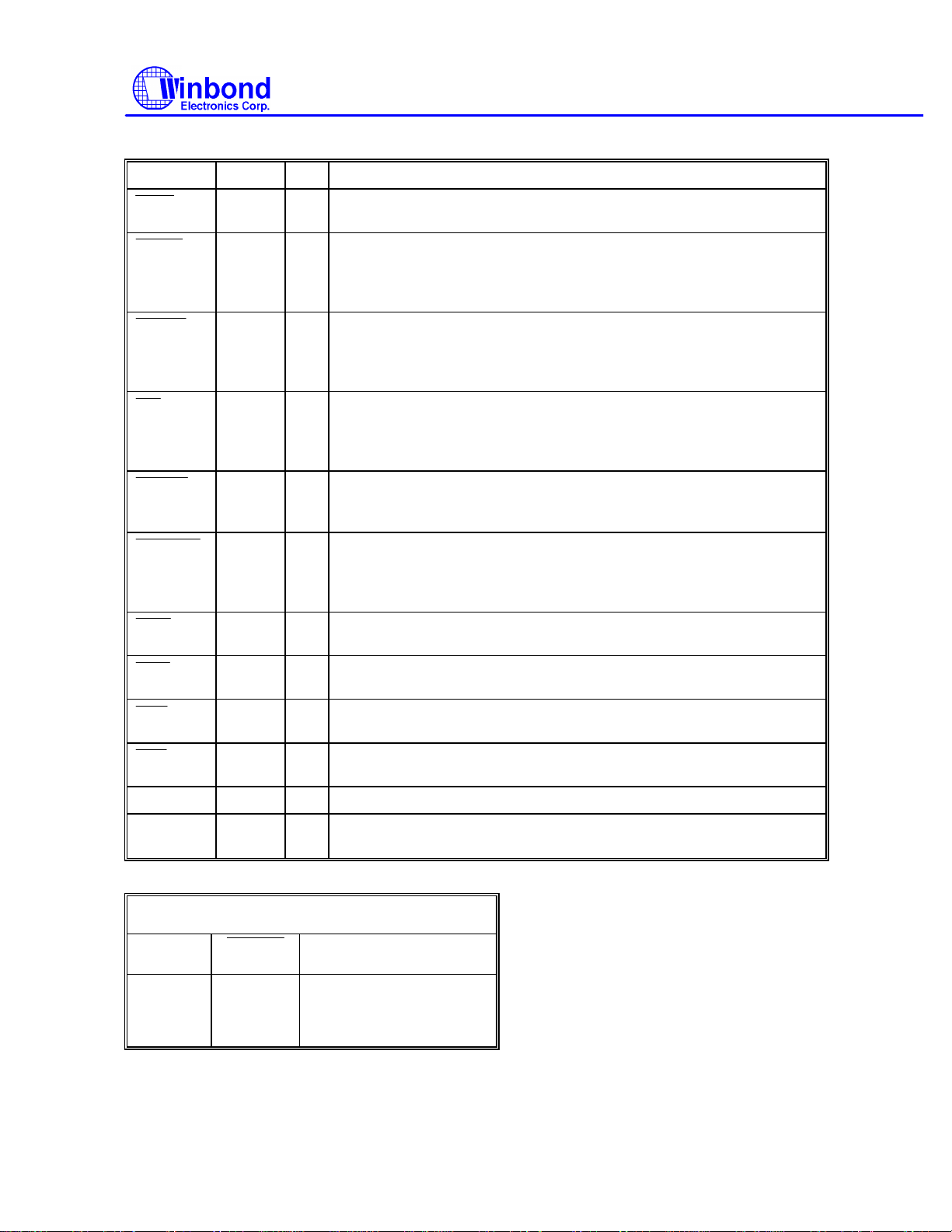
IDE and FDC Interface, continued
STEP
INDEX
TRAK
0
WP
RDATA
DSKCHG
MOA
MOB
DSA
DSB
GMWR
SYMBOL PIN I/O FUNCTION
W83787IF
82 OD
81 I
78 I
77 I
74 I
76 I
79 OD
80 OD
83 OD
84 OD
VDD 15, 56
Step output pulses. This active low open drain output produces a
pulse to move the head to another track.
This schmitt input from the disk drive is active low when the head is
positioned over the beginning of a track marked by an index hole.
This input pin is pulled up internally by an approximately 1K ohm
resistor. The resistor can be disabled by bit 4 of CR6 (FIPURDWN).
Track 0. This schmitt input from the disk drive is active low when the
head is positioned over the outermost track. This input pin is pulled
up internally by an approximately 1K ohm resistor. The resistor can
be disabled by bit 4 of CR6 (FIPURDWN).
Write protected. This active low schmitt input from the disk drive
indicates that the diskette is write-protected. This input pin is pulled
up internally by an approximately 1K ohm resistor. The resistor can
be disabled by bit 4 of CR6 (FIPURDWN).
The read data input signal from the FDD. This input pin is pulled up
internally by an approximately 1K ohm resistor. The resistor can be
disabled by bit 4 of CR6 (FIPURDWN).
Diskette change. This signal is active low at power on and whenever
the diskette is removed. This input pin is pulled up internally by an
approximately 1K ohm resistor. The resistor can be disabled by bit 4
of CR6 (FIPURDWN).
Motor A On. When set to 0, this pin enables disk drive 0. This is an
open drain output.
Motor B On. When set to 0, this pin enables disk drive 1. This is an
open drain output.
Drive Select A. When set to 0, this pin enables disk drive A. This is
an open drain output.
Drive Select B. When set to 0, this pin enables disk drive B. This is
an open drain output.
+5 power supply for the digital circuitry
GND 25, 40
65, 90
Table 1-1:
PARALLEL PORT FUNCTION MODE
POWER-ON SETTING
PDRQX
HPRTM1
L L Printer Mode (Default)
L H ECP/EPP
H L EPP
H H EXT2FDD
HPRTM0
Ground
Publication Release Date:Sep 1995
- 18 - Revision A1
Page 19

Table 1-2:
DTRB
RTSB
RTSA
DTRA
UART A UART B
SOUTA
HURAS1
L L COM4 (2E8) L L COM3 (3E8)
L H COM3 (3E8) L H COM4 (2E8)
H L COM1 (3F8) (Default) H L COM2 (2F8) (Default)
H H Disabled H H Disabled
Table 1-3 :
HURAS0
PARALLEL PORT
SOUTB
HURBS
HURBS0
W83787IF
HPRTS1
L L LPT3 (3BC)
L H LPT2 (278)
H L LPT1 (378) (Default)
H H Disabled
Note: When the parallel port is disabled, the eight function modes (W83757 mode, EXTFDD mode, EXTADP mode, EXT2FDD
mode, JOYSTICK mode, EPP mode, ECP mode, and ECP/EPP mode) are all inhibited.
Table 1-4 :
PIN W83787F/777F W83787IF
1 nRESIDE
2 PDBDIR/nFDCEN
3 PDCIN
42 SINB
43 SOUTB/HURBS1
91 nDBENL/ABCHG
92 nDBENH/FADSEL
93 nIOCS16 nIOCS16
HPRTS0
nRESIDE/IRRX3
PDBDIR/IRTX2/nFDCEN
PDCIN/IRRX2
SINB/IRRX1
SOUTB/IRTX1/HURBS1
nDBENL/nIDBEN/GIOSEL
nDBENH/GIO0/URIRSEL
94 nCS0/nIDEEN
95 nCS1/HADSEL
96 IDED7
nCS0/IRRX4/nIDEEN
nCS1/IRTX3/HADSEL
IDED7/GIO1
Publication Release Date:Sep 1995
- 19 - Revision A1
Page 20

W83787IF
2.0 FDC FUNCTIONAL DESCRIPTION
2.1 W83787IF FDC
The floppy disk controller of the W83787IF integrates all of the logic required for floppy disk
control.The FDC includes the following blocks: AT interface, Precompensation, Data Rate Selection,
Digital Data Separator, and FDC Core.
2.1.1 AT interface
The interface consists of the standard asynchronous signals: /RD, /WR, A0-A3, IRQ, DMA control,
and a data bus. The address lines select between the configuration registers, the FIFO and
control/status registers.
2.1.2 Data Separator
The function of the data separator is to lock onto the incoming serial read data. When a lock is
achieved the serial front end logic of the chip is provided with a clock which is synchronized to the
read data. The synchronized clock, called the Data Window, is used to internally sample the serial
data portion of the bit cell, and the alternate state samples the clock portion. Serial to parallel
conversion logic separates the read data into clock and data bytes.
The Digital Data Separator (DDS) has three parts: control logic, error adjustment, and speed tracking.
The DDS circuit cycles once every 12 clock cycles ideally. Any data pulse input will be synchronized
and then adjusted by immediate error adjustment. The control logic will generate RDD and RWD for
every pulse input. During any cycle where no data pulse is present, the DDS cycles are based on
speed. A digital integrator is used to keep track of the speed changes in the input data stream.
2.1.3 Write Precompensation
The write precompensation logic is used to minimize bit shifts in the RDDATA stream from the disk
drive. Shifting of bits is a known phenomenon in magnetic media and is dependent on the disk media
and the floppy drive.
The FDC monitors the bit stream that is being sent to the drive. The data patterns that require
precompensation are well known. Depending upon the pattern, the bit is shifted either early or late
relative to the surrounding bits.
2.1.4 FDC Core
The W83787IF FDC is capable of performing sixteen commands. Each command is initiated by a
multi-byte transfer from the microprocessor. The result can also be a multi-byte transfer back to the
microprocessor. Each command consists of three phases: command, execution, and result.
Command
The microprocessor issues all required information to the controller to perform a specific operation.
Execution
The controller performs the specified operation.
Result
After the operation is completed, status information and other housekeeping information is provided
to the microprocessor.
Publication Release Date:Sep 1995
- 20 - Revision A1
Page 21

2.1.5 FDC Commands
Command Symbol Descriptions:
C: Cylinder number 0 - 256
D: Data Pattern
DIR: Step Direction
DIR = 0, step out
DIR = 1, step in
DS0: Disk Drive Select 0
DS1: Disk Drive Select 1
DTL: Data Length
EC: Enable Count
EOT: End of Track
EFIFO: Enable FIFO
EIS: Enable Implied Seek
EOT: End of track
FIFOTHR: FIFO Threshold
GAP: Gap length selection
GPL: Gap Length
H: Head number
HDS: Head number select
HLT: Head Load Time
HUT: Head Unload Time
LOCK: Lock EFIFO, FIFOTHR, PTRTRK bits prevent affected by software reset
MFM: MFM or FM Mode
MT: Multitrack
N: The number of data bytes written in a sector
NCN: New Cylinder Number
ND: Non-DMA Mode
OW: Overwritten
PCN: Present Cylinder Number
POLL: Polling Disable
PRETRK: Precompensation Start Track Number
R: Record
RCN: Relative Cylinder Number
R/W: Read/Write
SC: Sector/per cylinder
SK: Skip deleted data address mark
SRT: Step Rate Time
ST0: Status Register 0
ST1: Status Register 1
ST2: Status Register 2
ST3: Status Register 3
WG: Write gate alters timing of WE
W83787IF
Publication Release Date:Sep 1995
- 21 - Revision A1
Page 22

(1) Read Data
PHASE R/W D7 D6 D5 D4 D3 D2 D1 D0 REMARKS
W83787IF
Command
Execution Data transfer between the
Result
W MT MFM SK 0 0 1 1 0
W 0 0 0 0 0 HDS DS1 DS0
W
W
W
W
W
W
W -------------------- DTL -----------------------
R
R
R
R
R
R
R
---------------------- C ------------------------
---------------------- H ------------------------
---------------------- R ------------------------
---------------------- N ------------------------
-------------------- EOT -----------------------
-------------------- GPL -----------------------
-------------------- ST0 -----------------------
-------------------- ST1 -----------------------
-------------------- ST2 -----------------------
---------------------- C ------------------------
---------------------- H ------------------------
---------------------- R ------------------------
---------------------- N ------------------------
Command codes
Sector ID information prior
to command execution
FDD and system
Status information after
command execution
Sector ID information after
command execution
(2) Read Deleted Data
PHASE R/W D7 D6 D5 D4 D3 D2 D1 D0 REMARKS
Command
Execution Data transfer between the
W MT MFM SK 0 1 1 0 0
W
W
W
W
W
W
W
W -------------------- DTL -----------------------
0 0 0 0 0 HDS DS1 DS0
---------------------- C ------------------------
---------------------- H ------------------------
---------------------- R ------------------------
---------------------- N ------------------------
-------------------- EOT -----------------------
-------------------- GPL -----------------------
- 22 - Revision A1
Command codes
Sector ID information prior
to command execution
FDD and system
Publication Release Date:Sep 1995
Page 23

Read Deleted Data,Continued
PHASE R/W D7 D6 D5 D4 D3 D2 D1 D0 REMARKS
W83787IF
Result
(3) Read A Track
PHASE R/W D7 D6 D5 D4 D3 D2 D1 D0 REMARKS
Command
Execution Data transfer between the
Result
R
R
R
R
R
R
R
W 0 MFM 0 0 0 0 1 0
W 0 0 0 0 0 HDS DS1 DS0
W
W
W
W
W
W
W -------------------- DTL -----------------------
R
R
R
R
R
R
R
-------------------- ST0 -----------------------
-------------------- ST1 -----------------------
-------------------- ST2 -----------------------
---------------------- C ------------------------
---------------------- H ------------------------
---------------------- R ------------------------
---------------------- N ------------------------
---------------------- C ------------------------
---------------------- H ------------------------
---------------------- R ------------------------
---------------------- N ------------------------
-------------------- EOT -----------------------
-------------------- GPL -----------------------
-------------------- ST0 -----------------------
-------------------- ST1 -----------------------
-------------------- ST2 -----------------------
---------------------- C ------------------------
---------------------- H ------------------------
---------------------- R ------------------------
---------------------- N ------------------------
Status information after
command execution
Sector ID information after
command execution
Command codes
Sector ID information prior
to command execution
FDD and system; FDD
reads contents of all
cylinders from index hole to
EOT
Status information after
command execution
Sector ID information after
command execution
Publication Release Date:Sep 1995
- 23 - Revision A1
Page 24

(4) Read ID
PHASE R/W D7 D6 D5 D4 D3 D2 D1 D0 REMARKS
W83787IF
Command
Execution The first correct ID
Result
(5) Write Data
PHASE R/W D7 D6 D5 D4 D3 D2 D1 D0 REMARKS
Command
Execution Data transfer between the
Result
W 0 MFM 0 0 1 0 1 0
W 0 0 0 0 0 HDS DS1 DS0
R
R
R
R
R
R
R
W MT MFM 0 0 0 1 0 1
W 0 0 0 0 0 HDS DS1 DS0
W
W
W
W
W
W
W -------------------- DTL -----------------------
R
R
R
R
R
R
R
-------------------- ST0 -----------------------
-------------------- ST1 -----------------------
-------------------- ST2 -----------------------
---------------------- C ------------------------
---------------------- H ------------------------
---------------------- R ------------------------
---------------------- N ------------------------
---------------------- C ------------------------
---------------------- H ------------------------
---------------------- R ------------------------
---------------------- N ------------------------
-------------------- EOT -----------------------
-------------------- GPL -----------------------
-------------------- ST0 -----------------------
-------------------- ST1 -----------------------
-------------------- ST2 -----------------------
---------------------- C ------------------------
---------------------- H ------------------------
---------------------- R ------------------------
---------------------- N ------------------------
Command codes
information on the cylinder
is stored in Data Register
Status information after
command execution
Disk status after the
command has been
completed
Command codes
Sector ID information prior
to Command execution
FDD and system
Status information after
Command execution
Sector ID information after
Command execution
Publication Release Date:Sep 1995
- 24 - Revision A1
Page 25

(6) Write Deleted Data
PHASE R/W D7 D6 D5 D4 D3 D2 D1 D0 REMARKS
W83787IF
Command W MT MFM 0 0 1 0 0 1
W 0 0 0 0 0 HDS DS1 DS0
W
W
W
W
W
W
W
Execution
Result R
R
R
R
R
R
R
---------------------- C ------------------------
---------------------- H ------------------------
---------------------- R ------------------------
---------------------- N ------------------------
-------------------- EOT -----------------------
-------------------- GPL -----------------------
-------------------- DTL -----------------------
-------------------- ST0 -----------------------
-------------------- ST1 -----------------------
-------------------- ST2 -----------------------
---------------------- C ------------------------
---------------------- H ------------------------
---------------------- R ------------------------
---------------------- N ------------------------
Command codes
Sector ID information prior
to command execution
Data transfer between the
FDD and system
Status information after
command execution
Sector ID information after
command execution
Publication Release Date:Sep 1995
- 25 - Revision A1
Page 26
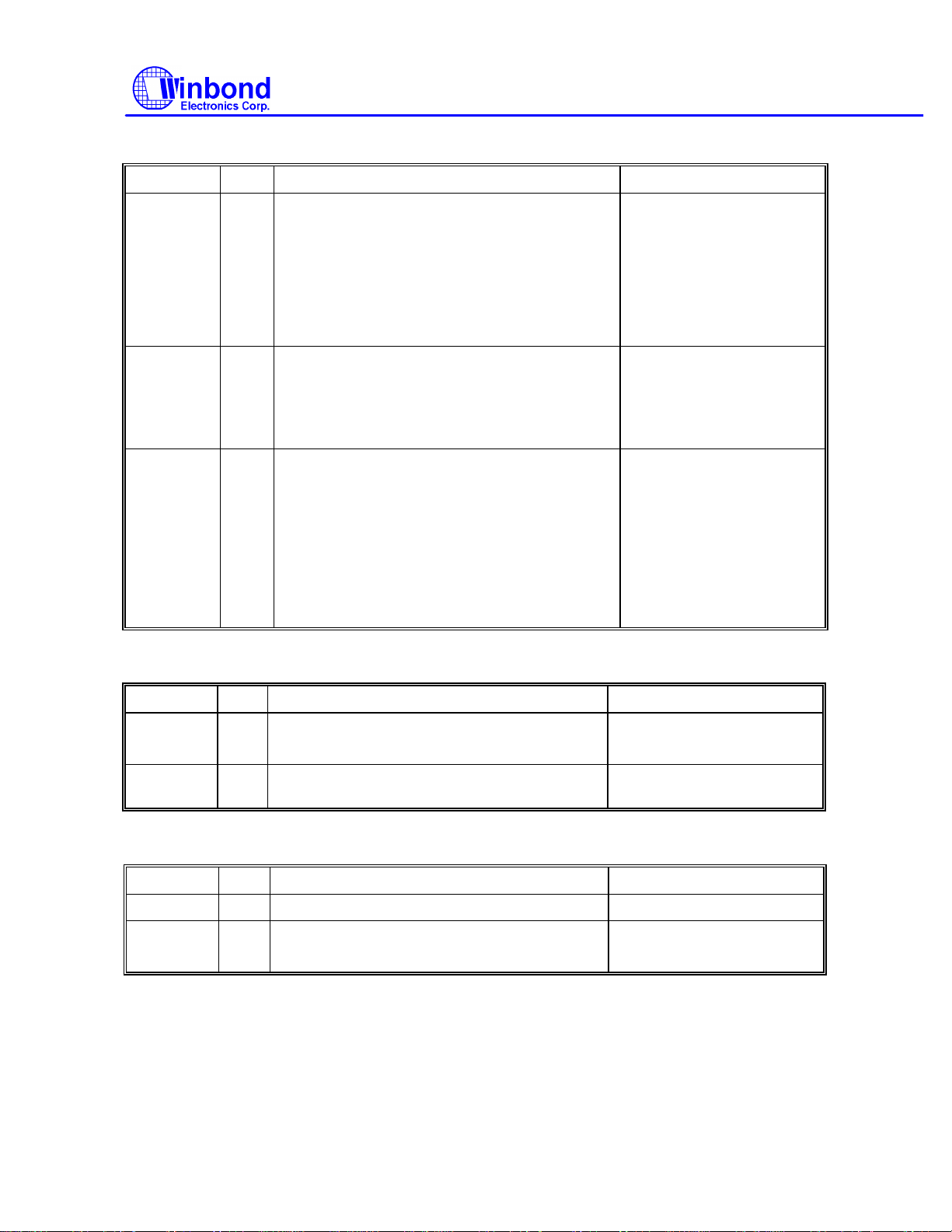
(7) Format A Track
PHASE R/W D7 D6 D5 D4 D3 D2 D1 D0 REMARKS
W83787IF
Command
Execution
for Each
Sector
Repeat:
Result
W 0 MFM 0 0 1 1 0 1
W 0 0 0 0 0 HDS DS1 DS0
W
W
W
W
W
W
W
W
R
R
R
R
R
R
R
---------------------- N ------------------------
--------------------- SC -----------------------
--------------------- GPL ---------------------
---------------------- D ------------------------
---------------------- C ------------------------
---------------------- H ------------------------
---------------------- R ------------------------
---------------------- N ------------------------
-------------------- ST0 -----------------------
-------------------- ST1 -----------------------
-------------------- ST2 -----------------------
---------------- Undefined -------------------
---------------- Undefined -------------------
---------------- Undefined -------------------
---------------- Undefined -------------------
Command codes
Bytes/Sector
Sectors/Cylinder
Gap 3
Filler Byte
Input Sector Parameters
Status information after
command execution
(8) Recalibrate
PHASE R/W D7 D6 D5 D4 D3 D2 D1 D0 REMARKS
Command
Execution Head retracted to Track 0
(9) Sense Interrupt Status
PHASE R/W D7 76 D5 D4 D3 D2 D1 D0 REMARKS
Command
Result
W 0 0 0 0 0 1 1 1
W 0 0 0 0 0 0 DS1 DS0
W 0 0 0 0 1 0 0 0
R
R
---------------- ST0 -------------------------
---------------- PCN -------------------------
Command codes
Interrupt
Command code
Status information at the
end of each seek operation
Publication Release Date:Sep 1995
- 26 - Revision A1
Page 27

(10) Specify
PHASE R/W D7 D6 D5 D4 D3 D2 D1 D0 REMARKS
W83787IF
Command
(11) Seek
PHASE R/W D7 D6 D5 D4 D3 D2 D1 D0 REMARKS
Command
Execution
(12) Sense Drive Status
PHASE R/W D7 D6 D5 D4 D3 D2 D1 D0 REMARKS
Command
Result R ---------------- ST3 -------------------------
W 0 0 0 0 0 0 1 1
W
W
W 0 0 0 0 1 1 1 1 Command codes
W
W
R
| ---------SRT ----------- | --------- HUT ---------- |
|------------ HLT ----------------------------------| ND
0 0 0 0 0 HDS DS1 DS0
-------------------- NCN -----------------------
W 0 0 0 0 0 1 0 0
W 0 0 0 0 0 HDS DS1 DS0
Command codes
Head positioned over
proper cylinder on diskette
Command Code
Status information about
disk drive
(13) Invalid
PHASE R/W D7 D6 D5 D4 D3 D2 D1 D0 REMARKS
Command
Result
W ------------- Invalid Codes -----------------
R -------------------- ST0 ----------------------
- 27 - Revision A1
Invalid codes (no operation
- FDC goes into standby
state)
ST0 = 80H
Publication Release Date:Sep 1995
Page 28

(14) Scan Equal
PHASE R/W D7 D6 D5 D4 D3 D2 D1 D0 REMARKS
W83787IF
Command
PHASE R/W D7 D6 D5 D4 D3 D2 D1 D0 REMARKS
Execution Data compare between the
Result
W MT MFM SK 1 0 0 0 1
W 0 0 0 0 0 HDS DS1 DS0
W
W
W
W
W
W
W -------------------- DTL -----------------------
R
R
R
R
R
R
R
---------------------- C ------------------------
---------------------- H ------------------------
---------------------- R ------------------------
---------------------- N ------------------------
-------------------- EOT -----------------------
-------------------- GPL -----------------------
-------------------- ST0 -----------------------
-------------------- ST1 -----------------------
-------------------- ST2 -----------------------
---------------------- C ------------------------
---------------------- H ------------------------
---------------------- R ------------------------
---------------------- N ------------------------
Command codes
Sector ID information prior
to command execution
FDD and system
Status information after
command execution
Sector ID information after
command execution
Publication Release Date:Sep 1995
- 28 - Revision A1
Page 29

(15) Scan Low or Equal
PHASE R/W D7 D6 D5 D4 D3 D2 D1 D0 REMARKS
W83787IF
Command
Execution Data compare between
Result
W MT MFM SK 1 1 0 0 1
W 0 0 0 0 0 HDS DS1 DS0
W
W
W
W
W
W
W -------------------- DTL -----------------------
R
R
R
R
R
R
R
---------------------- C ------------------------
---------------------- H ------------------------
---------------------- R ------------------------
---------------------- N ------------------------
-------------------- EOT -----------------------
-------------------- GPL -----------------------
-------------------- ST0 -----------------------
-------------------- ST1 -----------------------
-------------------- ST2 -----------------------
---------------------- C ------------------------
---------------------- H ------------------------
---------------------- R ------------------------
---------------------- N ------------------------
Command codes
Sector ID information prior
to command execution
the FDD and system
Status information after
command execution
Sector ID information after
command execution
Publication Release Date:Sep 1995
- 29 - Revision A1
Page 30

(16) Scan High or Equal
PHASE R/W D7 D6 D5 D4 D3 D2 D1 D0 REMARKS
W83787IF
Comman
d
Execution Data compare between the
Result
W MT MFM SK 1 1 1 0 1
W 0 0 0 0 0 HDS DS1 DS0
W
W
W
W
W
W
W -------------------- DTL -----------------------
R
R
R
R
R
R
R
---------------------- C ------------------------
---------------------- H ------------------------
---------------------- R ------------------------
---------------------- N ------------------------
-------------------- EOT -----------------------
-------------------- GPL -----------------------
-------------------- ST0 -----------------------
-------------------- ST1 -----------------------
-------------------- ST2 -----------------------
---------------------- C ------------------------
---------------------- H ------------------------
---------------------- R ------------------------
---------------------- N ------------------------
Command codes
Sector ID information prior
to command execution
FDD and system
Status information after
command execution
Sector ID information after
command execution
2.3 Register Descriptions
There are status, data, and control registers in the W83787IF. The addresses of these registers are
defined below:
ADDRESS REGISTER
PRIMARY SECONDARY READ WRITE
3F2
3F3
3F4 374 MS REGISTER Reserved
3F5 375 DT REGISTER DT REGISTER
3F7 377 DI REGISTER CC REGISTER
372
373
DO REGISTER
TD REGISTER
Publication Release Date:Sep 1995
- 30 - Revision A1
Page 31
W83787IF
Floppy boot drive 0
Floppy boot drive 1
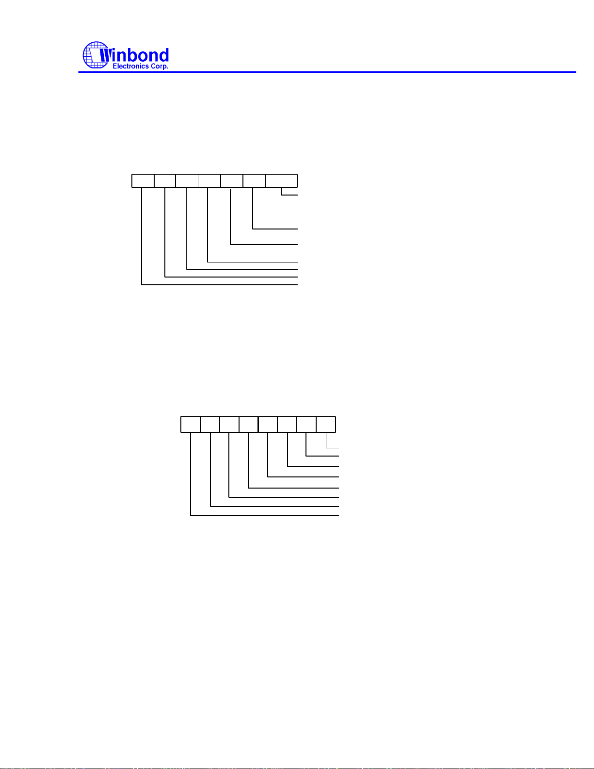
2.3.1 Digital Output Register (DO Register) (Write 3F2H/372H)
The Digital Output Register is a write-only register controlling drive motors, drive selection, DRQ/IRQ
enable, and FDC resetting. All the bits in this register are cleared by the MR pin. The bit definitions
are as follows:
7 6
5 4
3
1-0
2
Drive Select: 00 select drive A
Floppy Disk Controller Reset
Active low resets FDC
DMA and INT Enable
Active high enable DRQ/IRQ
Motor Enable A. Motor A on when active high
Motor Enable B. Motor B on when active high
Motor Enable C. Motor C on when active high
Motor Enable D. Motor D on when active high
01 select drive B
10 select drive C
11 select drive D
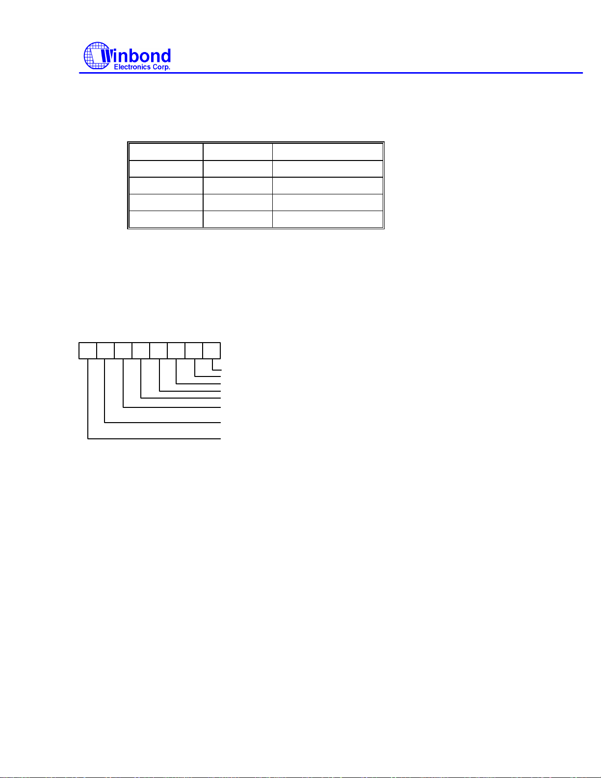
2.3.2 Tape Drive Register (TD Register) (Read 3F3H/373H)
This register is used to assign a particular drive number to the tape drive support mode of the data
separator. This register also holds the media ID, drive type, and floppy boot drive information of the
floppy disk drive.If three mode FDD function is enabled (EN3MODE =1 in CR9), the bit definitions are
as follows (W83787IF):
2
34567
1
0
Tape Sel 0
Tape Sel 1
Media ID1 Media ID0 (Bit 7, 6):
These two bits are read only. These two bits reflect the value of CR8 bit 3, 2.
Drive type ID1 Drive type ID0 (Bit 5, 4):
These two bits reflect two of the bits of CR7. Which two bits are reflected depends on the last drive
selected in the DO REGISTER.
Floppy Boot drive 1, 0 (Bit 3, 2):
These two bits reflect the value of CR8 bit 1, 0.
Drive type ID0
Drive type ID1
Media ID0
Media ID1
Publication Release Date:Sep 1995
- 31 - Revision A1
Page 32
W83787IF
Tape Sel 1, Tape Sel 0 (Bit 1, 0):
These two bits assign a logical drive number to the tape drive. Drive 0 is not available as a tape drive
and is reserved as the floppy disk boot drive.
TAPE SEL 1 TAPE SEL 0 DRIVE SELECTED
0 0 None
0 1 1
1 0 2
1 1 3
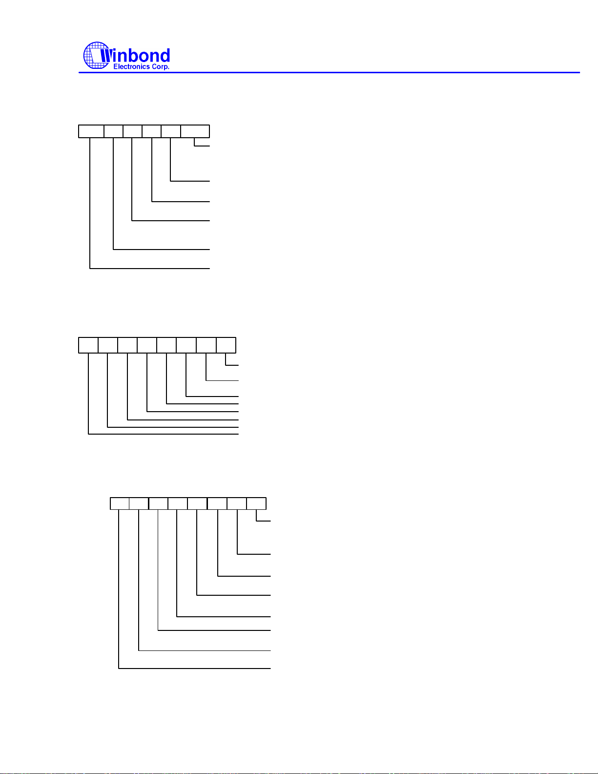
2.3.3 Main Status Register (MS Register) (Read 3F4H/374H)
The Main Status Register is used to control the flow of data between the microprocessor and the
controller. The bit definitions for this register are as follows:
6
7
4
5
3 2 1
0
FDD 0 Busy, (D0B=1), FDD number 0 is in the SEEK mode.
FDD 1 Busy, (D1B=1), FDD number 1 is in the SEEK mode.
FDD 2 Busy, (D2B=1), FDD number 2 is in the SEEK mode.
FDD 3 Busy, (D3B=1), FDD number 3 is in the SEEK mode.
FDC Busy, (CB). A read or write command is in the process when CB= HIGH.
Non-DMA mode, the FDC is in the non-DMA mode, this bit is set only during the execution phase in non-DMA mode.
Transition to LOW state indicates execution phase has ended.
DATA INPUT/OUTPUT, (DIO). If DIO= HIGH then transfer is from Data Register to the processor.
If DIO= LOW then transfer is from processor to Data Register.
Request for Master (RQM). A high on this bit indicates Data Register is ready to send or receive data to or from the processor.
2.3.4 DATA Register (DT Register ) (R/W 3F5H/375H)
The Data Register consists of four status registers in a stack with only one register presented to the
data bus at a time. This register stores data, commands, and parameters and provides diskette-drive
status information. Data bytes are passed through the data register to program or obtain results after
a command.
Publication Release Date:Sep 1995
- 32 - Revision A1
Page 33
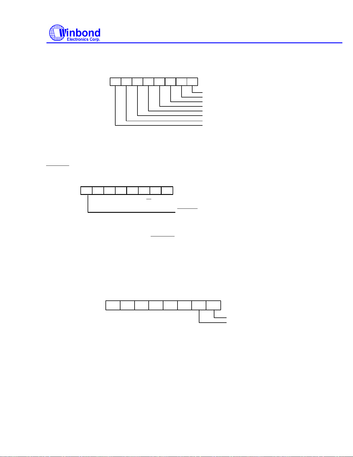
Status Register 0 (ST0)
11 Abnormal termination because the ready signal from FDD changed state during command execution
OR (Over Rum). 1 If the FDC is not serviced by the host system within a certain time interval during data transfer.
1 During execution of the Scan command, if the equal condition is satisfied
W83787IF
7-6 5
3 2 1-0
4
Status Register 1 (ST1)
US1, US0 Drive Select:
00 Drive A selected
01 Drive B selected
10 Drive C selected
11 Drive D selected
HD Head address:
1 Head selected
0 Head selected
NR Not Ready:
1 Drive is not ready
0 Drive is ready
EC Equipment Check:
1 When a fault signal is received from the FDD or the track
0 signal fails to occur after 77 step pulses
0 No error
SE Seek end:
1 seek end
0 seek error
IC Interrupt Code:
00 Normal termination of command
01 Abnormal termination of command
10 Invalid command issue
234567
01
Missing Address Mark. 1 When the FDC cannot detect the data address mark
or the data address mark has been deleted.
NW (Not Writable). 1 If a write Protect signal is detected from the diskette drive during
execution of write data.
ND (No DATA). 1 If specified sector cannot be found during execution of a read, write or verifly data.
Not used. This bit is always 0.
DE (data Error).1 When the FDC detects a CRC error in either the ID field or the data field.
Not used. This bit is always 0.
EN (End of track). 1 When the FDC tries to access a sector beyond the final sector of a cylinder.
Status Register 2 (ST2)
7 0
56
1
234
MD (Missing Address Mark in Data Field).
1 If the FDC cannot find a data address mark
(or the address mark has been deleted)
when reading data from the media
0 No error
BC (Bad Cylinder)
1 Bad Cylinder
0 No error
SN (Scan Not satisfied)
1 During execution of the Scan command
0 No error
SH (Scan Equal Hit)
0 No error
WC (Wrong Cylinder)
1 Indicates wrong Cylinder
DD (Data error in the Data field)
1 If the FDC detects a CRC error in the data field
0 No error
CM (Control Mark)
1 During execution of the read data or scan command
0 No error
Not used. This bit is always 0
Publication Release Date:Sep 1995
- 33 - Revision A1
Page 34
Status Register 3 (ST3)
WP Write Protected
DSKCHG
x
DSKCHG
W83787IF
6
7
4
5
3
12
0
US0 Unit Select 0
US1 Unit Select 1
HD Head Address
TS Two-Side
TO Track 0
RY Ready
FT Fault
2.3.5 Digital Input Register (DI Register) (Read 3F7H/377H)
The Digital Input Register is an 8-bit read-only register used for diagnostic purposes. In a PC/XT or
AT only Bit 7 is checked by the BIOS. When the register is read, Bit 7 shows the complement of
, while other bits of the data bus remain in tri-state. Bit definitions are as follows:
567
xxx
x
DSKCHG (Bit 7):
This bit indicates the complement of the
01234
xxx
Reserved for the hard disk controller
During a read of this register, these bits are in tri-state
DSKCHG
input.
Bit 6-3: These bits are always a logic 1 during a read.
2.3.6 Configuration Control Register (CC Register) (Write 3F7H/377H)
This register is used to control the data rate. In the PC/AT and PS/2 mode, the bit definitions are as
follows:
4
5
6
7
2
3
1
0
x x x x x x
DRATE0
DRATE1
X: Reserved
Bit 7-2: Reserved. These bits should be set to 0.
DRATE1 DRATE0 (Bit 1, 0):
These two bits select the data rate of the FDC.
Publication Release Date:Sep 1995
- 34 - Revision A1
Page 35
W83787IF
CS
0
CS
0
CS
1
CS
1
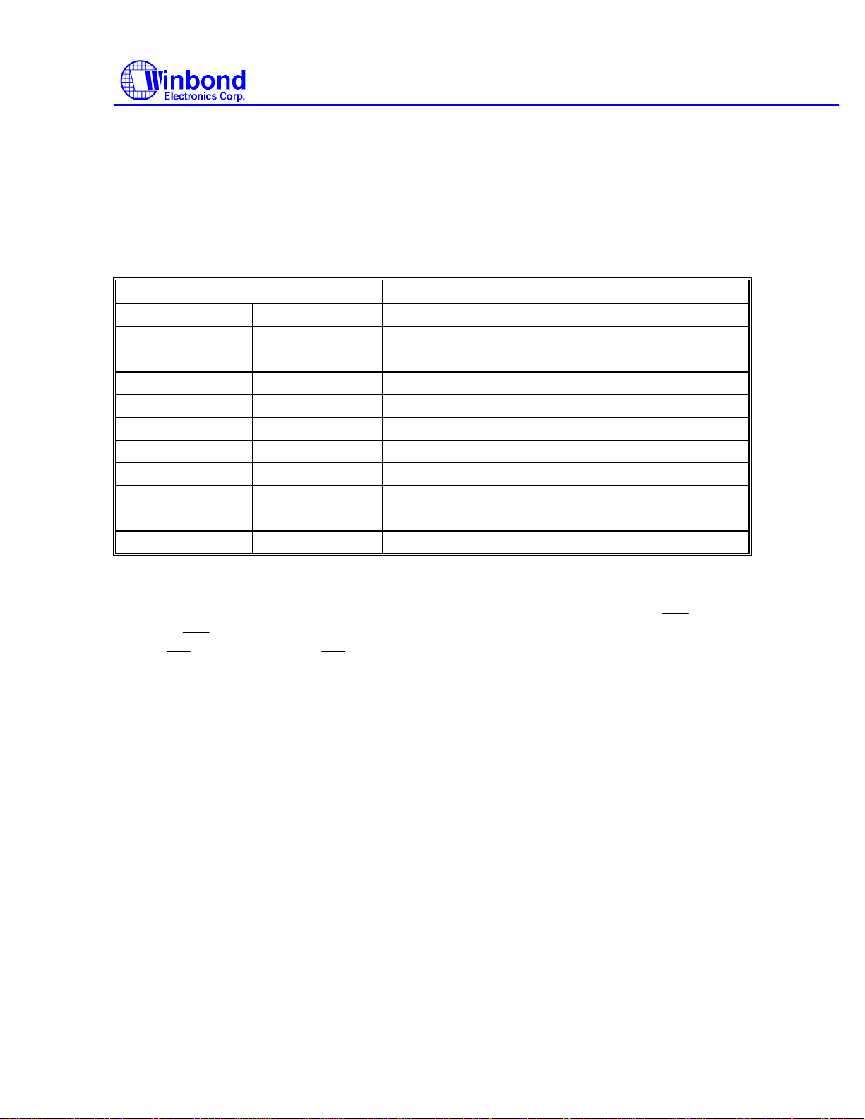
3.0 IDE
The IDE interface is essentially the AT bus ported to the hard disk drive. The hard disk controller
resides on the IDE hard disk drive. So the IDE interface provides only chip select signals and AT bus
signals between the IDE hard disk drive and ISA slot. Table 3-1 shows the IDE registers and their ISA
addresses.
Table 3-1
I/O ADDRESS REGISTERS
PRIMARY SECONDARY READ WRITE
1F0 170 Data Register Data Register
1F1 171 Error Register Write-Precomp
1F2 172 Sector Count Sector Count
1F3 173 Sector Number Sector Number
1F4 174 Cylinder LOW Cylinder LOW
1F5 175 Cylinder HIGH Cylinder HIGH
1F6 176 SDH Register SDH Register
1F7 177 Status Register Command Register
3F6 376 Alternate Status Fixed Disk Control
3F7 377 Digital Input Undefined
3.1 IDE Decode Description
When the processor selects Ports 1F0-1F7 (or 170-177), the chip system enables
otherwise,
enables
= HIGH. When the processor selects Ports 3F6-3F7 (or 376-377), the chip system
= LOW; otherwise,
= HIGH.
= LOW;
4.0 UART PORT
4.1 Universal Asynchronous Receiver/Transmitter (UART A, UART B)
The UARTs are used to convert parallel data into serial format on the transmit side and convert serial
data to parallel format on the receiver side. The serial format, in order of transmission and reception,
is a start bit, followed by five to eight data bits, a parity bit (if programmed) and one, one and half
(five-bit format only) or two stop bits. The UARTs are capable of handling divisors of 1 to 65536 and
producing a 16x clock for driving the internal transmitter logic. Provisions are also included to use this
16x clock to drive the receiver logic. The UARTs also support the MIDI data rate. Furthermore, the
UARTs also include complete modem control capability and a processor interrupt system that may be
software trailed to the computing time required to handle the communication link. The UARTs have a
FIFO mode to reduce the number of interrupts presented to the CPU. In each UART, there are 16byte FIFOs for both receive and transmit mode.
Publication Release Date:Sep 1995
- 35 - Revision A1
Page 36

W83787IF
4.2 Register Address
TABLE 4 - 2 UART Register Bit Map
Bit Number
Register Address Base 0 1 2 3 4 5 6 7
8
BDLAB = 0
8
BDLAB = 0
9
BDLAB = 0
A Interrupt Status
A UART FIFO
B UART Control
C Handshake
D UART Status
E Handshake
F User Defined
8
BDLAB = 1
9
BDLAB = 1
*: Bit 0 is the least significant bit. The least significant bit is the first bit serially transmitted or received.
**: These bits are always 0 in 16450 Mode.
Receiver
Buffer
Register
(Read Only)
Transmitter
Buffer Register
(Write Only)
Interrupt Control
Register
Register
(Read Only)
Control
Register
(Write Only)
Register
Control
Register
Register
Status Register
Register
Baudrate Divisor
Latch Low
Baudrate
Divisor Latch
High
RBR RX Data
Bit 0
TBR TX Data
Bit 0
ICR RBR Data
Ready
Interrupt
Enable
(ERDRI)
ISR "0" if
Interrupt
Pending
UFR FIFO
Enable
UCR Data
Length
Select
Bit 0
(DLS0)
HCR Data
Terminal
Ready
(DTR)
USR RBR Data
Ready
(RDR)
HSR CTS
Toggling
(TCTS)
UDR Bit 0 Bit 1 Bit 2 Bit 3 Bit 4 Bit 5 Bit 6 Bit 7
BLL Bit 0 Bit 1 Bit 2 Bit 3 Bit 4 Bit 5 Bit 6 Bit 7
BHL Bit 8 Bit 9 Bit 10 Bit 11 Bit 12 Bit 13 Bit 14 Bit 15
RX Data
Bit 1
TX Data
Bit 1
TBR
Empty
Interrupt
Enable
(ETBREI)
Interrupt
Status
Bit (0)
RCVR
FIFO
Reset
Data
Length
Select
Bit 1
(DLS1)
Request
to
Send
(RTS)
Overrun
Error
(OER)
DSR
Toggling
(TDSR)
RX Data
Bit 2
TX Data
Bit 2
USR
Interrupt
Enable
(EUSRI)
Interrupt
Status
Bit (1)
XMIT
FIFO
Reset
Multiple
Stop Bits
Enable
(MSBE)
Loopback
RI
Input
Parity Bit
Error
(PBER)
RI Falling
Edge
(FERI)
RX Data
Bit 3
TX Data
Bit 3
HSR
Interrupt
Enable
(EHSRI)
Interrupt
Status
Bit (2)**
DMA
Mode
Select
Parity
Bit
Enable
(PBE)
IRQ
Enable
No Stop
Bit
Error
(NSER)
DCD
Toggling
(TDCD)
RX Data
Bit 4
TX Data
Bit 4
Reserved Reversed RX
Even
Parity
Enable
(EPE)
Internal
Loopback
Enable
Silent
Byte
Detected
(SBD)
Clear
to Send
(CTS)
RX Data
Bit 5
TX Data
Bit 5
0 0 0 0
0 0 FIFOs
Parity
Bit Fixed
Enable
PBFE)
TBR
Empty
(TBRE)
Data Set
Ready
(DSR)
RX Data
Bit 6
TX Data
Bit 6
Enabled
**
Interrupt
Active
Level
(LSB)
Set
Silence
Enable
(SSE)
0 0 0
TSR
Empty
(TSRE)
Ring
Indicator
(RI)
RX Data
Bit 7
TX Data
Bit 7
FIFOs
Enabled
**
RX
Interrupt
Active
Level
(MSB)
Baudrate
Divisor
Latch
Access Bit
(BDLAB)
RX FIFO
Error
Indication
(RFEI) **
Data
Carrier
Detect
(DCD)
Publication Release Date:Sep 1995
- 36 - Revision A1
Page 37
W83787IF
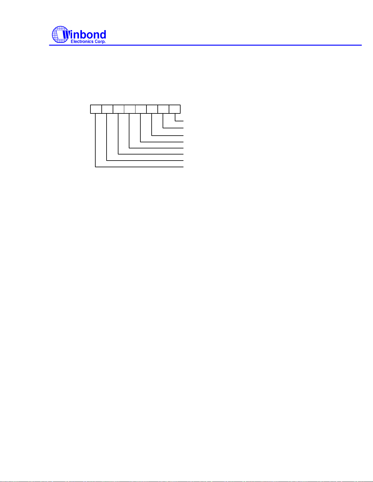
Baudrate divisor latch access bit (BDLAB)
4.2.1 UART Control Register (UCR) (Read/Write)
The UART Control Register controls and defines the protocol for asynchronous data communications,
including data length, stop bit, parity, and baud rate selection.
6
7 0
45
2
3
1
Data length select bit 0 (DLS0)
Data length select bit 1(DLS1)
Multiple stop bits enable (MSBE)
Parity bit enable (PBE)
Even parity enable (EPE)
Parity bit fixed enable (PBFE)
Set silence enable (SSE)
Notes:
Bit 7: BDLAB. When this bit is set to a logical 1, designers can access the divisor (in 16-bit
binary format) from the divisor latches of the baudrate generator during a read or write
operation. When this bit is reset, the Receiver Buffer Register, the Transmitter Buffer Register,
or the Interrupt Control Register can be accessed.
Bit 6: SSE. A logical 1 forces the Serial Output (SOUT) to a silent state (a logical 0). Only SOUT
is affected by this bit; the transmitter is not affected.
Bit 5: PBFE. When PBE and PBFE of UCR are both set to a logical 1,
(1) if EPE is a logical 1, the parity bit is fixed as a logical 0 to transmit and check.
(2) if EPE is a logical 0, the parity bit is fixed as a logical 1 to transmit and check.
Bit 4: EPE. This bit describes the number of logic 1's in the data word bits and parity bit only when
bit 3 is programmed. When this bit is set, an even number of logic 1's are sent or checked.
When the bit is reset, an odd number of logic 1's are sent or checked.
Bit 3: PBE. When this bit is set, the position between the last data bit and the stop bit of the SOUT
will be stuffed with the parity bit at the transmitter. For the receiver, the parity bit in the same
position as the transmitter will be detected.
Bit 2: MSBE. This bit defines the number of stop bits in each serial character that is transmitted or
received.
(1) If MSBE is set to a logical 0, one stop bit is sent and checked.
(2) If MSBE is set to a logical 1, and data length is 5 bits, one and a half stop bits are sent and
checked.
(3) If MSBE is set to a logical 1, and data length is 6, 7, or 8 bits, two stop bits are sent and
checked.
Bits 0 and 1: DLS0, DLS1. These two bits define the number of data bits that are sent or checked in
each serial character.
Publication Release Date:Sep 1995
- 37 - Revision A1
Page 38
W83787IF
TABLE 4 - 3 WORD LENGTH DEFINITION
DLS1 DLS0 DATA LENGTH
0 0 5 bits
0 1 6 bits
1 0 7 bits
1 1 8 bits
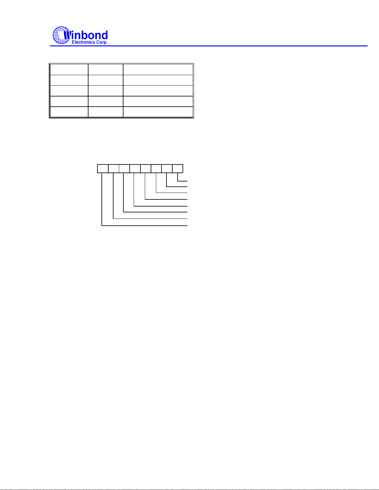
4.2.2 UART Status Register (USR) (Read/Write)
This 8-bit register provides information about the status of the data transfer during communication.
2
67 0
5
34
1
RBR Data ready (RDR)
Overrun error (OER)
Parity bit error (PBER)
No stop bit error (NSER)
Silent byte detected (SBD)
Transmitter Buffer Register empty (TBRE)
Transmitter Shift Register empty (TSRE)
RX FIFO Error Indication (RFEI)
Notes:
Bit 7: RFEI. In 16450 mode, this bit is always set to a logic 0. In 16550 mode, this bit is set to a logic
1 when there is at least one parity bit error, no stop bit error or silent byte detected in the FIFO.
In 16550 mode, this bit is cleared by reading from the USR if there are no remaining errors left
in the FIFO.
Bit 6: TSRE. In 16450 mode, when TBR and TSR are both empty, this bit will be set to a logical 1. In
16550 mode, if the transmit FIFO and TSR are both empty, it will be set to a logical 1. Other
than these two cases, this bit will be reset to a logical 0.
Bit 5: TBRE. In 16450 mode, when a data character is transferred from TBR to TSR, this bit will be
set to a logical 1. If ETREI of ICR is a logical 1, an interrupt will be generated to notify the CPU
to write the next data. In 16550 mode, this bit will be set to a logical 1 when the transmit FIFO
is empty. It will be reset to a logical 0 when the CPU writes data into TBR or FIFO.
Bit 4: SBD. This bit is set to a logical 1 to indicate that received data are kept in silent state for a
full word time, including start bit, data bits, parity bit, and stop bits. In 16550 mode, it
indicates the same condition for the data on top of the FIFO. When the CPU reads USR, it will
clear this bit to a logical 0.
Bit 3: NSER. This bit is set to a logical 1 to indicate that the received data have no stop bit. In 16550
mode, it indicates the same condition for the data on top of the FIFO. When the CPU reads
USR, it will clear this bit to a logical 0.
Bit 2: PBER. This bit is set to a logical 1 to indicate that the parity bit of received data is wrong. In
16550 mode, it indicates the same condition for the data on top of the FIFO. When the CPU
reads USR, it will clear this bit to a logical 0.
Bit 1: OER. This bit is set to a logical 1 to indicate received data have been overwritten by the next
received data before they were read by the CPU. In 16550 mode, it indicates the same
condition instead of FIFO full. When the CPU reads USR, it will clear this bit to a logical 0.
Publication Release Date:Sep 1995
- 38 - Revision A1
Page 39
W83787IF
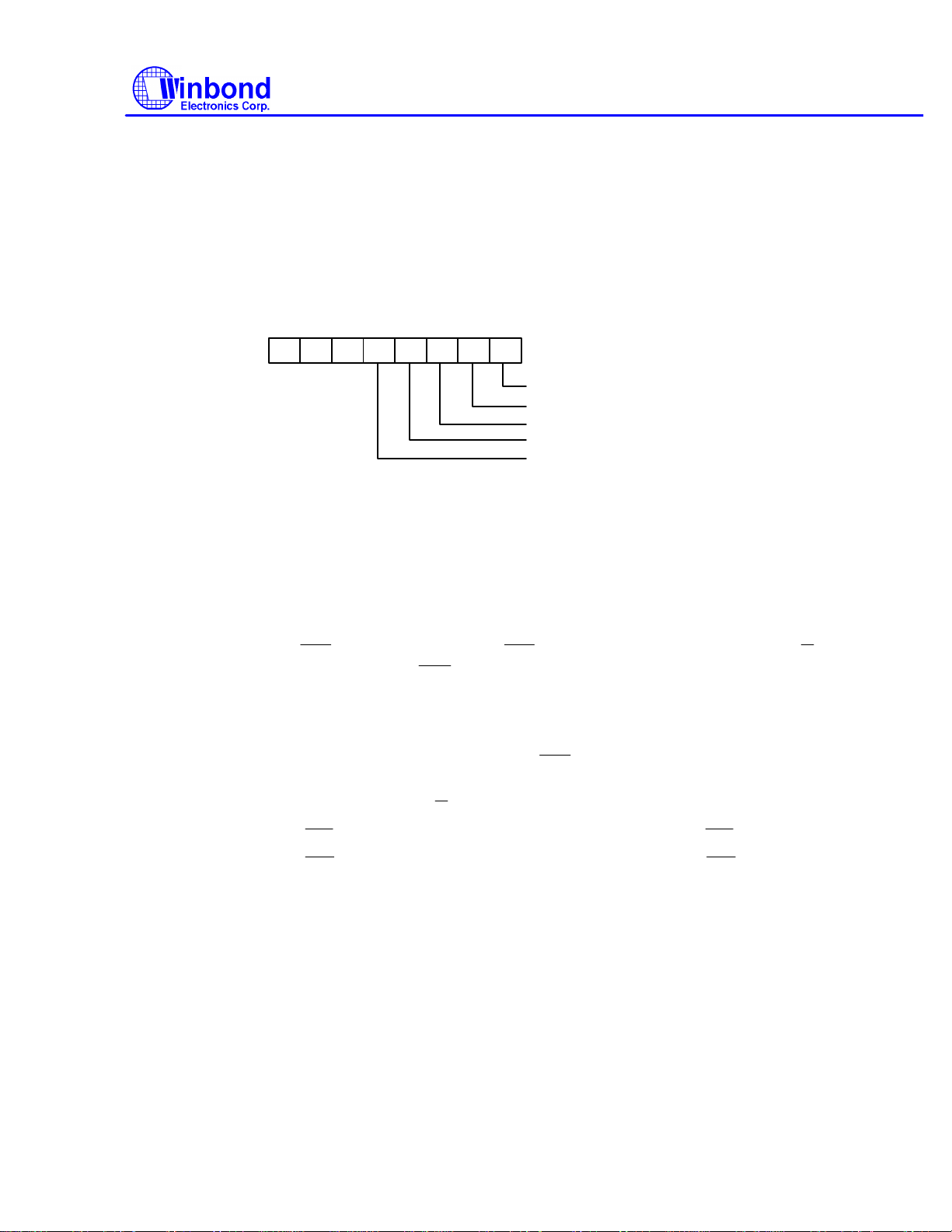
DSR
CTS
RI
DCD
DCD
RTS
RTS
DTR
DTR
Bit 0: RDR. This bit is set to a logical 1 to indicate received data are ready to be read by the CPU in
the RBR or FIFO. After no data are left in the RBR or FIFO, the bit will be reset to a logical 0.
4.2.3 Handshake Control Register (HCR) (Read/Write)
This register controls the pins of the UART used for handshaking peripherals such as modem, and
controls the diagnostic mode of the UART.
2
7
6
0
00
345
01
Data terminal ready (DTR)
Request to send (RTS)
Loopback RI input
IRQ enable
Internal loopback enable
Notes:
Bit 4: When this bit is set to a logical 1, the UART enters diagnostic mode by an internal loopback,
as follows:
(1) SOUT is forced to a logical 1, and SIN is isolated from the communication link instead of
the TSR.
(2) Modem output pins are set to their inactive state.
(3) Modem input pins are isolated from the communication link and connect internally as DTR
(bit 0 of HCR) →
and IRQ enable ( bit 3 of HCR) →
, RTS ( bit 1 of HCR) →
.
, Loopback RI input ( bit 2 of HCR) →
Aside from the above connections, the UART operates normally. This method allows the
CPU to test the UART in a convenient way.
Bit 3: The UART interrupt output is enabled by setting this bit to a logic 1. In the diagnostic mode this
bit is internally connected to the modem control input
.
Bit 2: This bit is used only in the diagnostic mode. In the diagnostic mode this bit is internally
connected to the modem control input RI.
Bit 1: This bit controls the
Bit 0: This bit controls the
output. The value of this bit is inverted and output to
output. The value of this bit is inverted and output to
Publication Release Date:Sep 1995
- 39 - Revision A1
.
.
Page 40
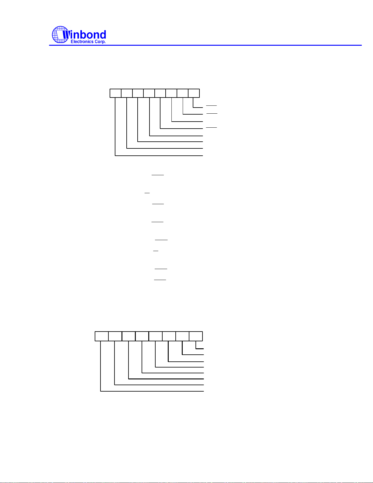
W83787IF
DCD
DSR
CTS
DCD
DSR
CTS
4.2.4 Handshake Status Register (HSR) (Read/Write)
This register reflects the current state of four input pins for handshake peripherals such as a modem
and records changes on these pins.
1234567 0
toggling (TCTS)
CTS
toggling (TDSR)
DSR
RI falling edge (FERI)
toggling (TDCD)
DCD
Clear to send (CTS)
Data set ready (DSR)
Ring indicator (RI)
Data carrier detect (DCD)
Notes:
Bit 7: This bit is the opposite of the
input. This bit is equivalent to bit 3 of HCR in loopback
mode.
Bit 6: This bit is the opposite of the RI input. This bit is equivalent to bit 2 of HCR in loopback mode.
Bit 5: This bit is the opposite of the
input. This bit is equivalent to bit 0 of HCR in loopback
mode.
Bit 4: This bit is the opposite of the
input. This bit is equivalent to bit 1 of HCR in loopback
mode.
Bit 3: TDCD. This bit indicates that the
pin has changed state after HSR was read by the CPU.
Bit 2: FERI. This bit indicates that the RI pin has changed from low to high state after HSR was read
by the CPU.
Bit 1: TDSR. This bit indicates that the
Bit 0: TCTS. This bit indicates that the
pin has changed state after HSR was read by the CPU.
pin has changed state after HSR was read by the CPU.
4.2.5 UART FIFO Control Register (UFR) (Write only)
This register is used to control the FIFO functions of the UART.
34567 0
12
FIFO enable
Receiver FIFO reset
Transmitter FIFO reset
DMA mode select
Reserved
Reserved
RX interrupt active level (LSB)
RX interrupt active level (MSB)
Notes: Bit 6, 7: These two bits are used to set the active level for the receiver FIFO interrupt. For
example, if the interrupt active level is set as 4 bytes, once there are more than 4 data characters in
the receiver FIFO, the interrupt will be activated to notify the CPU to read the data from the FIFO.
Publication Release Date:Sep 1995
- 40 - Revision A1
Page 41
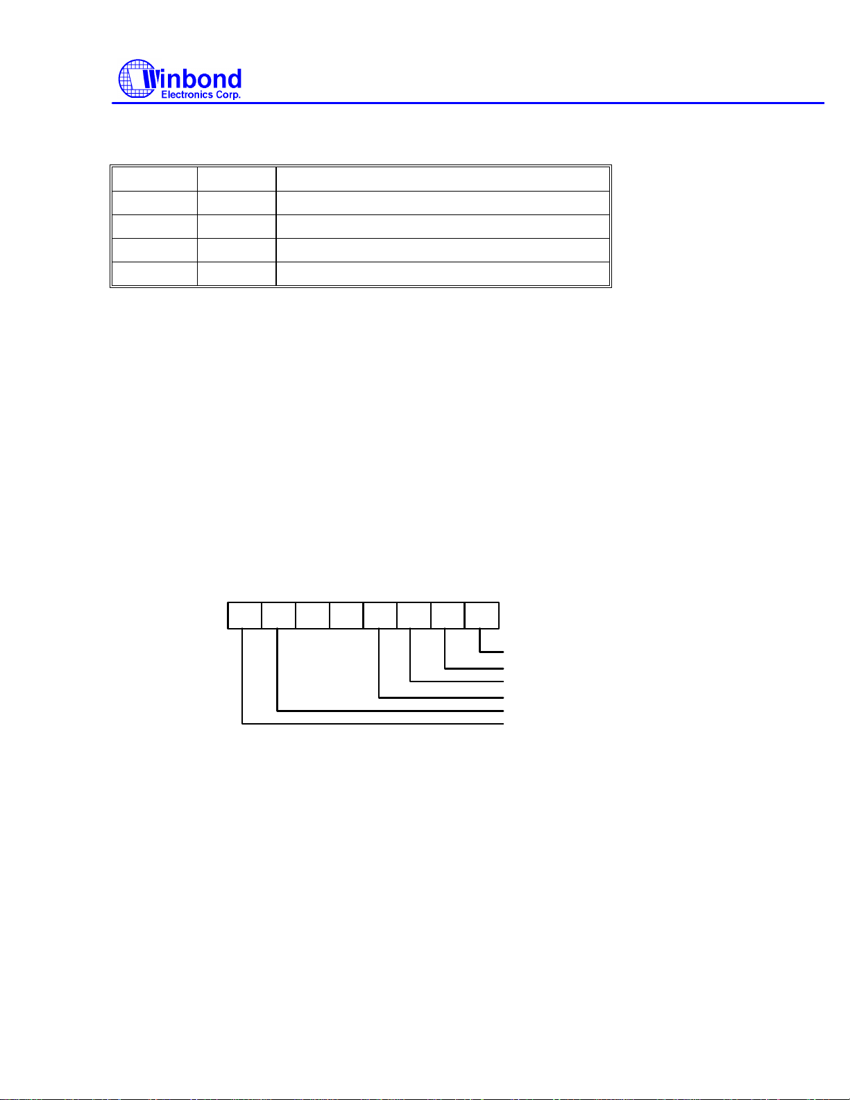
W83787IF
0 if interrupt pending
Interrupt Status bit 0
Interrupt Status bit 1
Interrupt Status bit 2
TABLE 4-4 FIFO TRIGGER LEVEL
BIT 7 BIT 6 RX FIFO INTERRUPT ACTIVE LEVEL (BYTES)
0 0 01
0 1 04
1 0 08
1 1 14
Bit 4, 5: Reserved
Bit 3: When this bit is programmed to logic 1, the DMA mode will change from mode 0 to mode 1 if
UFR bit 0 = 1.
Bit 2: Setting this bit to a logical 1 resets the TX FIFO counter logic to initial state. This bit will clear to
a logical 0 by itself after being set to a logical 1.
Bit 1: Setting this bit to a logical 1 resets the RX FIFO counter logic to initial state. This bit will clear to
a logical 0 by itself after being set to a logical 1.
Bit 0: This bit enables the 16550 (FIFO) mode of the UART. This bit should be set to a logical 1
before other bits of UFR are programmed.
4.2.6 Interrupt Status Register (ISR) (Read only)
This register reflects the UART interrupt status, which is encoded by different interrupt sources into 3
bits.
1234567
0
0 0
FIFOs enabled
FIFOs enabled
Notes:
Bit 7, 6: These two bits are set to a logical 1 when UFR bit 0 = 1.
Bit 5, 4: These two bits are always logic 0.
Bit 3: In 16450 mode, this bit is 0. In 16550 mode, both bit 3 and 2 are set to a logical 1 when a
time-out interrupt is pending.
Bit 2, 1: These two bits identify the priority level of the pending interrupt, as shown in the table below.
Bit 0: This bit is a logical 1 if there is no interrupt pending. If one of the interrupt sources has
occurred, this bit will be set to a logical 0.
Publication Release Date:Sep 1995
- 41 - Revision A1
Page 42
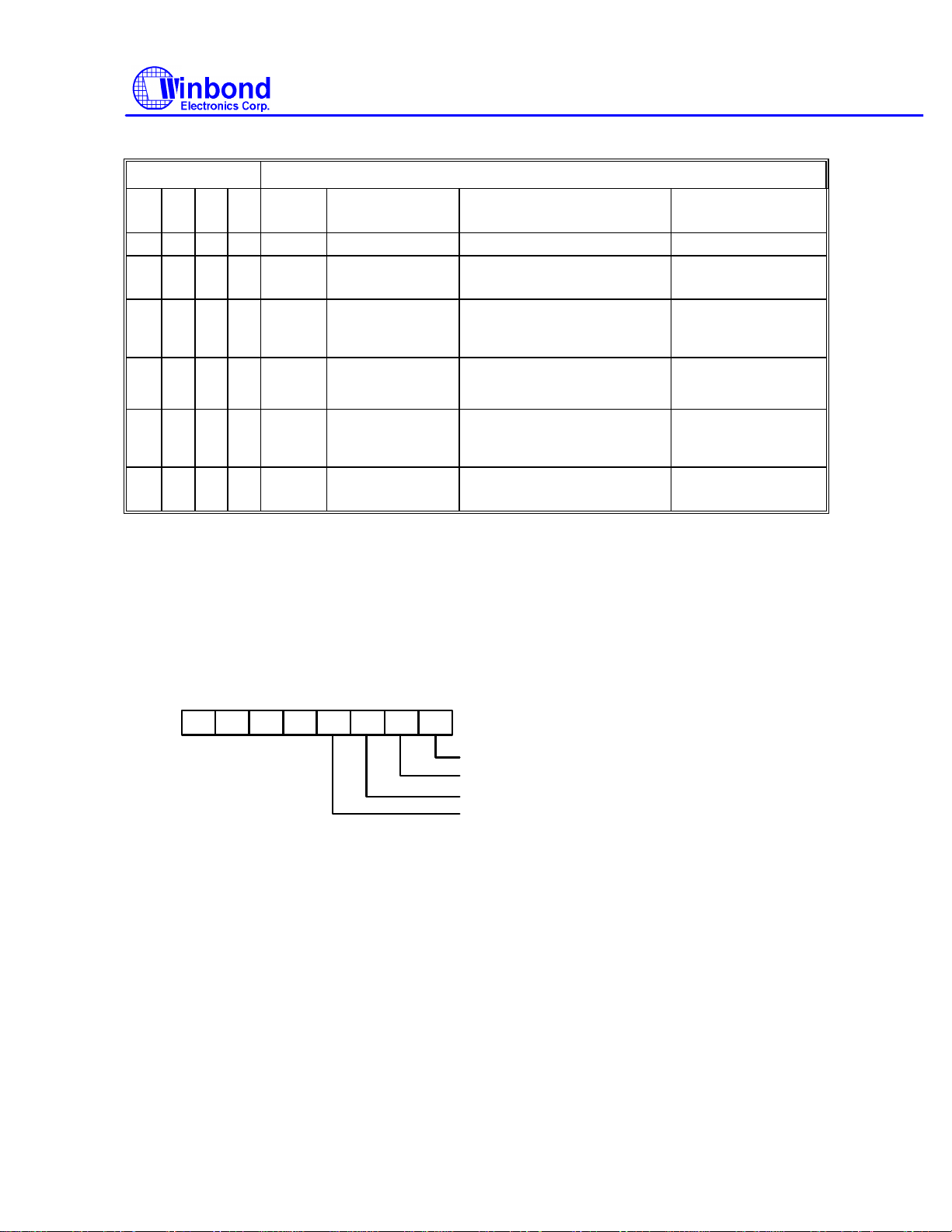
TABLE 4-5 INTERRUPT CONTROL FUNCTION
ISR INTERRUPT SET AND FUNCTION
Bit3Bit2Bit1Bit
0
Interrupt
priority
Interrupt Type Interrupt Source Clear Interrupt
W83787IF
0 0 0 1 - 0 1 1 0
0 1 0 0
1 1 0 0
0 0 1 0
0 0 0 0
** Bit 3 of ISR is enabled when bit 0 of UFR is logical 1.
First UART Receive
Status
Second RBR Data Ready 1. RBR data ready
Second FIFO Data Timeout Data present in RX FIFO for 4
Third TBR Empty TBR empty 1. Write data into TBR
Fourth Handshake status 1. TCTS = 1 2. TDSR = 1
No Interrupt pending
1. OER = 1 2. PBER =1
3. NSER = 1 4. SBD = 1
2. FIFO interrupt active level
reached
characters period of time since last
access of RX FIFO.
3. FERI = 1 4. TDCD = 1
-
Read USR
1. Read RBR
2. Read RBR until FIFO
data under active level
Read RBR
2. Read ISR (if priority is
third)
Read HSR
4.2.7 Interrupt Control Register (ICR) (Read/Write)
This 8-bit register allows the five types of controller interrupts to activate the interrupt output signal
separately. The interrupt system can be totally disabled by resetting bits 0 through 3 of the Interrupt
Control Register (ICR). A selected interrupt can be enabled by setting the appropriate bits of this
register to a logical 1.
7
0
5
6
0 0 0
3
4
2
0
1
RBR data ready interrupt enable (ERDRI)
TBR empty interrupt enable (ETBREI)
UART receive status interrupt enable (EUSRI)
Handshake status interrupt enable (EHSRI)
Notes:
Bit 7-4: These four bits are always logic 0.
Bit 3: EHSRI. Setting this bit to a logical 1 enables the handshake status register interrupt.
Bit 2: EUSRI. Setting this bit to a logical 1 enables the UART status register interrupt.
Bit 1: ETBREI. Setting this bit to a logical 1 enables the TBR empty interrupt.
Bit 0: ERDRI. Setting this bit to a logical 1 enables the RBR data ready interrupt.
Publication Release Date:Sep 1995
- 42 - Revision A1
Page 43

W83787IF
4.2.8 Programmable Baud Generator (BLL/BHL) (Read/Write)
Two 8-bit registers, BLL and BHL, compose a programmable baud generator that uses 24 MHz to
generate a 1.8461 MHz frequency and divides it by a divisor from 1 to 216-1. The output frequency of
the baud generator is the baud rate multiplied by 16, and this is the base frequency for the transmitter
and receiver. The following table illustrates the use of the baud generator with frequency of 1.8461
Mhz. In high speed UART mode (refer CR0C.bit7 and CR0C.bit6), the programmable baud generator
directly uses 24 MHZ and the divider which is same as normal speed divisor. In the high speed mode,
the data transmission rate can be up to 1.5 M bps.
TABLE 4-6 BAUD RATE TABLE
BAUD RATE USING 24 MHZ TO GENERATE 1.8461 MHZ
Desired Baud Rate Decimal divisor used to
generate 16X clock
50 2304 **
75 1536 **
110 1047 0.18%
134.5 857 0.099%
150 768 **
300 384 **
600 192 **
1200 96 **
1800 64 **
2000 58 0.53%
2400 48 **
3600 32 **
4800 24 **
7200 16 **
9600 12 **
19200 6 **
38400 3 **
57600 2 **
115200 1 **
230400 104* **
460800 52* **
921600 26* **
1.5M 1* 0%
* Only use in high speed mode (refer CR0C.bit7 and CR0C.bit6).
** The percentage error for all baud rates, except where indicated otherwise, is 0.16%.
Percent error difference
between desired and actual
Publication Release Date:Sep 1995
- 43 - Revision A1
Page 44

W83787IF
4.2.9 User-defined Register (UDR) (Read/Write)
This is a temporary register that can be accessed and defined by the user.
4.2.10 IRQ3/IRQ4 Setting
IRQ3 and IRQ4 are the interrupt pins for UARTA and UARTB in the W83787IF. These two interrupt
pins switch automatically inside the chip depending on the address setting of UARTA and UARTB.
When the address of UARTA or UARTB is selected as COM1 or COM3, interrupt requests for the
UART are sent out of W83787IF via IRQ4. If the address of UARTA or UARTB is selected as COM2
or COM4, interrupts are sent out via IRQ3. Thus when UARTA is set as COM1, UARTB should not be
set as COM3, and vice versa. When UARTA is set as COM2, UARTB should not be set as COM4,
and vice versa.
4.3 Infrared Interface
The infrared interface supports a two-way wireless communication using infrared as a
transceiver/receive media. It uses a UART B port to serve as data transmission and supports IrDA
and Amplitude Shift Keyed IR (ASK-IR).
In the IrDA mode, the serial transmission maximum baud rate can be up to 115.2k. When the UART
B send a zero signal, the IRTX encoder encodes a pulse width with 3/16 bit-time or fixed 1.6us to
output on IR emitter. If UART B send a high signal, then the encoder have no data output to IR
emitter. The decoder receiving a pulse with 3/16 bit-time or 1.6us represents a start bit. (Refer to AC
timing for the parameters of the IrDA waveform).
In the ASK-IR mode, the serial transmission maximum baud rate is only 19200 bps. When the UART
B send a zero signal, the encoder modulate 500KHZ sending to IR emitter. (Refer to AC timing for the
parameters of the ASK-IR waveform).
In the half duplex, the receiver does not receive any input data when transceiver transmit data. That
is, during the transmission, the receiver does not disturb it-self from the self-emitter.
5.0 PARALLEL PORT
5.1 Printer Interface Logic
The parallel port of the W83787IF makes possible the attachment of various devices that accept eight
bits of parallel data at standard TTL level. The W83787IF supports an IBM XT/AT compatible parallel
port (SPP), bi-directional parallel port (BPP), Enhanced Parallel Port (EPP), Extended Capabilities
Parallel Port (ECP), Extension FDD mode (EXTFDD), Extension 2FDD mode (EXT2FDD), Extension
Adapter mode (EXTADP), and JOYSTICK mode on the parallel port. Refer to the configuration
registers for more information on disabling, power-down, and changing the base address of the
parallel port and on selecting the mode of operation.
Table 5-1 shows the pin definitions for different modes of the parallel port.
Publication ReleaseDate:Sep 1995
- 44 - Revision A1
Page 45
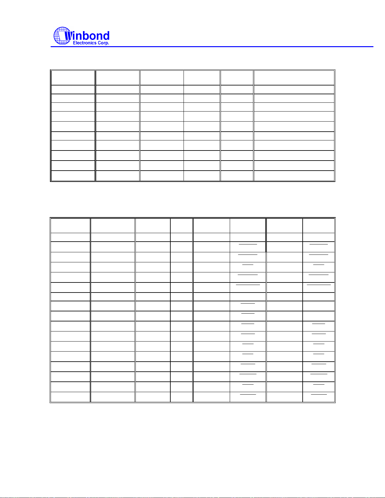
TABLE 5-1 PARALLEL PORT CONNECTOR AND PIN DEFINITIONS
INDEX
2IINDEX
2
TRAK
02ITRAK
02
WP
2IWP
2
RDATA
2IRDATA
2
DSKCHG
2IDSKCHG
2
MOA
2
DSA
2
DSB
2ODDSB
2
MOB
2ODMOB
2
WD
2ODWD
2
WE
2ODWE
2
RWC
2ODRWC
2
NERR
2ODNERR
2
DIR
2ODDIR
2
STEP
2ODSTEP
2
HOST
CONNECTOR
1 19 O nSTB nWrite nSTB
2-9 9-14,16-17 I/O PD<0:7> PD<0:7> PD<0:7>
10 26 I nACK Intr nACK
11 24 I BUSY nWait
12 27 I PE PE
13 28 I SLCT Select SLCT
14 20 O nAFD nDStrb
15 29 I nERR nError
16 21 O nINIT nInit
17 22 O nSLIN nAStrb
Notes:
n<name > : Active Low
1. Compatible Mode
2. High Speed Mode
3. For more information, refer to the IEEE 1284 standard.
PIN NUMBER
OF W83787I
PIN
ATTRIBUTE
SPP EPP ECP
W83787IF
BUSY, PeriphAck
PEerror, nAckReverse
nAFD, HostAck
nFault1, nPeriphRequest
nINIT1, nReverseRqst
1, 2
nSLIN
2
2
2
2
2
HOST
CONNECTOR
1 19 O nSTB --- --- --- --2 9 I/O PD0 I
3 10 I/O PD1 I
4 11 I/O PD2 I
5 12 I/O PD3 I
6 13 I/O PD4 I
7 14 I/O PD5 --- --- --- ---
8 15 I/O PD6 OD
9 16 I/O PD7 OD
10 26 I nACK OD
11 24 I BUSY OD
12 27 I PE OD
13 28 I SLCT OD
14 20 O nAFD OD
15 29 I nERR OD
16 21 O nINIT OD
17 22 O nSLIN OD
PIN NUMBER
OF W83787I
PIN
ATTRIBUTE
SPP PIN
ATTRIBUTE
EXT2FDD PIN
ATTRIBUTE
--- ---
--- ---
EXTFDD
Publication ReleaseDate:Sep 1995
- 45 - Revision A1
Page 46
W83787IF
XWR
XRD
XDACK
HOST
CONNECTOR
1 19 O nSTB O
2 9 I/O PD0 I/O XD0 I JP0
3 10 I/O PD1 I/O XD1 I JP1
4 11 I/O PD2 I/O XD2 I ---
5 12 I/O PD3 I/O XD3 I ---
6 13 I/O PD4 I/O XD4 I JB0
7 14 I/O PD5 I/O XD5 I JB1
8 15 I/O PD6 I/O XD6 I ---
9 16 I/O PD7 I/O XD7 I --10 26 I nACK I XDRQ I --11 24 I BUSY I XIRQ I --12 27 I PE O XA0 I --13 28 I SLCT O XA1 I --14 20 O nAFD O
15 29 I nERR O XA2 I --16 21 O nINIT O
17 22 O nSLIN O TC O VDD
PIN NUMBER
OF W83787I
PIN
ATTRIBUTE
SPP PIN
ATTRIBUTE
EXTADP
MODE
PIN
ATTRIBUTE
O VDD
O VDD
O VDD
JOYSTICK
MODE
5.2 Enhanced Parallel Port (EPP)
TABLE 5-2 PRINTER MODE AND EPP REGISTER ADDRESS
A2 A1 A0 REGISTER NOTE
0 0 0 Data port (R/W) 1
0 0 1 Printer status buffer (Read) 1
0 1 0 Printer control latch (Write) 1
0 1 0 Printer control swapper (Read) 1
0 1 1 EPP address port (R/W) 2
1 0 0 EPP data port 0 (R/W) 2
1 0 1 EPP data port 1 (R/W) 2
1 1 0 EPP data port 2 (R/W) 2
1 1 1 EPP data port 3 (R/W) 2
Notes:
1. These registers are available in all modes.
2. These registers are available only in EPP mode.
Publication ReleaseDate:Sep 1995
- 46 - Revision A1
Page 47
W83787IF
ACK
BUSY
5.2.1 Data Swapper
The system microprocessor can read the contents of the printer's data latch by reading the data
swapper.
5.2.2 Printer Status Buffer
The system microprocessor can read the printer status by reading the address of the printer status
buffer. The bit definitions are as follows:
1
235 467 0
1 1
TMOUT
ERROR
SLCT
PE
ACK
BUSY
Notes:
Bit 7: This signal is active during data entry, when the printer is off-line during printing, when the print
head is changing position, or during an error state. When this signal is active, the printer is
busy and cannot accept data.
Bit 6: This bit represents the current state of the printer's
received a character and is ready to accept another. Normally, this signal will be active for
approximately 5 microseconds before
stops.
Bit 5: A 1 means the printer has detected the end of paper.
Bit 4: A 1 means the printer is selected.
Bit 3: A 0 means the printer has encountered an error condition.
Bit 1, 2: These two bits are not implemented and are logic one during a read of the status register.
Bit 0: This bit is valid in EPP mode only. It indicates that a 10 µS timeout has occurred on the EPP
bus. A logic 0 means that no timeout error has occurred; a logic 1 means that a timeout error
has been detected. Writing a logic 1 to this bit will clear the timeout status bit; writing a logic 0
has no effect.
signal. A 0 means the printer has
5.2.3 Printer Control Latch and Printer Control Swapper
The system microprocessor can read the contents of the printer control latch by reading the printer
control swapper. Bit definitions are as follows:
234567 0
111
STROBE
AUTO FD
INIT
SLCT IN
IRQ ENABLE
DIR
Notes:
Bit 7, 6: These two bits are a logic one during a read. They can be written.
Bit 5: Direction control bit
Publication ReleaseDate:Sep 1995
- 47 - Revision A1
Page 48
W83787IF
PRTOE
ACK
IOW
IOW
IOR
IOW
W83757 (SPP) mode: When this bit is a logic 1, pin
is high, and PRTBEN (CR3 bit 7)
is low, the parallel port is in input mode (read); when this bit is a logic 0, the parallel port is in
output mode (write). This bit is write-only.
BPP mode: When this bit is a logic 1, the parallel port is in input mode (read); when it is a logic
0, the parallel port is in output mode (write). This bit can be read and written.
Bit 4: A 1 in this position allows an interrupt to occur when
changes from low to high.
Bit 3: A 1 in this bit position selects the printer.
Bit 2: A 0 starts the printer (50 microsecond pulse, minimum).
Bit 1: A 1 causes the printer to line-feed after a line is printed.
Bit 0: A 0.5 microsecond minimum high active pulse clocks data into the printer. Valid data must be
present for a minimum of 0.5 microseconds before and after the strobe pulse.
5.2.4 EPP Address Port
The address port is available only in EPP mode. Bit definitions are as follows:
1234567 0
PD0
PD1
PD2
PD3
PD4
PD5
PD6
PD7
The contents of DB0-DB7 are buffered (non-inverting) and output to ports PD0-PD7 during a write
operation. The leading edge of
trailing edge of
latches the data for the duration of the EPP write cycle.
PD0-PD7 ports are read during a read operation. The leading edge of
causes an EPP address write cycle to be performed, and the
causes an EPP address
read cycle to be performed and the data to be output to the host CPU.
5.2.5 EPP Data Port 0-3
These four registers are available only in EPP mode. Bit definitions of each data port are as follows:
7
123456
0
PD0
PD1
PD2
PD3
PD4
PD5
PD6
PD7
When accesses are made to any EPP data port, the contents of DB0-DB7 are buffered (noninverting) and output to the ports PD0-PD7 during a write operation. The leading edge of
causes
Publication ReleaseDate:Sep 1995
- 48 - Revision A1
Page 49
W83787IF
IOW
IOR
BUSY
ACK
ERROR
INIT
AUTOFD
STROBE
INIT
AUTOFD
STROBE
an EPP data write cycle to be performed, and the trailing edge of
duration of the EPP write cycle.
During a read operation, ports PD0-PD7 are read, and the leading edge of
cycle to be performed and the data to be output to the host CPU.
5.2.6 Bit Map of Parallel Port and EPP Registers
REGISTER 7 6 5 4 3 2 1 0
Data Port (R/W) PD7 PD6 PD5 PD4 PD3 PD2 PD1 PD0
Status Buffer (Read)
Control Swapper (Read) 1 1 1 IRQEN SLIN
Control Latch (Write) 1 1 DIR IRQ SLIN
EPP Address Port
(R/W)
EPP Data Port 0 (R/W) PD7 PD6 PD5 PD4 PD3 PD2 PD1 PD0
EPP Data Port 1 (R/W) PD7 PD6 PD5 PD4 PD3 PD2 PD1 PD0
EPP Data Port 2 (R/W) PD7 PD6 PD5 PD4 PD3 PD2 PD1 PD0
EPP Data Port 3 (R/W) PD7 PD6 PD5 PD4 PD3 PD2 PD1 PD0
PD7 PD6 PD5 PD4 PD3 PD2 PD1 PD0
PE SLCT
latches the data for the
causes an EPP read
1 1 TMOUT
5.2.7 EPP Pin Descriptions
EPP
NAME
nWrite O Denotes an address or data read or write operation.
PD<0:7>
Intr I Used by peripheral device to interrupt the host.
nWait I Inactive to acknowledge that data transfer is completed. Active to indicate
PE I Paper end; same as SPP mode.
Select I Printer selected status; same as SPP mode.
nDStrb O This signal is active low. It denotes a data read or write operation.
nError I Error; same as SPP mode.
nInits O This signal is active low. When it is active, the EPP device is reset to its
nAStrb O This signal is active low. It denotes an address read or write operation.
5.2.8 EPP Operation
When the EPP mode is selected in the configuration register, the standard and bi-directional modes
are also available. The PDx bus is in the standard or bi-directional mode when no EPP read, write, or
address cycle is currently being executed. In this condition all output signals are set by the SPP
Control Port and the direction is controlled by DIR of the Control Port.
TYPE EPP DESCRIPTION
I/O Bi-directional EPP address and data bus.
that the device is ready for the next transfer.
initial operating mode,
Publication ReleaseDate:Sep 1995
- 49 - Revision A1
Page 50

W83787IF
WAIT
A watchdog timer is required to prevent system lockup. The timer indicates that more than 10 µS
have elapsed from the start of the EPP cycle to the time
is aborted when a timeout occurs. The timeout condition is indicated in Status bit 0.
EPP Operation
The EPP operates on a two-phase cycle. First, the host selects the register within the device for
subsequent operations. Second, the host performs a series of read and/or write byte operations to the
selected register. Four operations are supported on the EPP: Address Write, Data Write, Address
Read, and Data Read. All operations on the EPP device are performed asynchronously.
EPP Version 1.9 Operation
The EPP read/write operation can be completed under the following conditions:
a. If the nWait is active low, when the read cycle (nWrite inactive high, nDStrb/nAStrb active low) or
write cycle (nWrite active low, nDStrb/nAStrb active low) starts, the read/write cycle proceeds
normally and will be completed when nWait goes inactive high.
b. If nWait is inactive high, the read/write cycle will not start. It must wait until nWait changes to
active low, at which time it will start as described above.
EPP Version 1.7 Operation
The EPP read/write cycle can start without checking whether nWait is active or inactive. Once the
read/write cycle starts, however, it will not terminate until nWait changes from active low to inactive
high.
is deasserted. The current EPP cycle
5.2.9 EPP Address Selection
More than four register addresses are required for EPP operation, so parallel port address 3BCh will
not support EPP mode when the parallel port is set up for W83757 mode or ECP mode, the SPP/BPP
will function normally in 3BCh, 378h, 278h. If 3BCh and EPP mode are selected, then the
SPP/BPP/EPP function will not be active.
5.3 Extended Capabilities Parallel (ECP) Port
This port is software and hardware compatible with existing parallel ports, so it may be used as a
standard printer mode if ECP is not required. It provides an automatic high burst-bandwidth channel
that supports DMA for ECP in both the forward (host to peripheral) and reverse (peripheral to host)
directions.
Small FIFOs are used in both forward and reverse directions to improve the maximum bandwidth
requirement. The size of the FIFO is 16 bytes. The ECP port supports an automatic handshake for
the standard parallel port to improve compatibility mode transfer speed.
The ECP port supports run-length-encoded (RLE) decompression (required) in hardware.
Compression is accomplished by counting identical bytes and transmitting an RLE byte that indicates
how many times the next byte is to be repeated. Hardware support for compression is optional.
For more information about the ECP Protocol, refer to the Extended Capabilities Port Protocol and
ISA Interface Standard.
Publication ReleaseDate:Sep 1995
- 50 - Revision A1
Page 51
W83787IF
5.3.1 ECP Register and Mode Definitions
NAME ADDRESS I/O ECP MODES FUNCTION
data Base+000h R/W 000-001 Data Register
ecpAFifo Base+000h R/W 011 ECP FIFO (Address)
dsr Base+001h R All Status Register
dcr Base+002h R/W All Control Register
cFifo Base+400h R/W 010 Parallel Port Data FIFO
ecpDFifo Base+400h R/W 011 ECP FIFO (DATA)
tFifo Base+400h R/W 110 Test FIFO
cnfgA Base+400h R 111 Configuration Register A
cnfgB Base+401h R/W 111 Configuration Register B
ecr Base+402h R/W All Extended Control Register
Note: The base addresses are 3BCH, 378H, and 278H, which are determined by configuration register or hardware setting.
MODE DESCRIPTION
000 SPP mode
001 PS/2 Parallel Port mode
010 Parallel Port Data FIFO mode
011 ECP Parallel Port mode
100 EPP mode (If this option is enabled in the CR9 and CR0 to select ECP/EPP mode)
101 Reserved
110 Test mode
111 Configuration mode
Note: The mode selection bits are bit 7-5 of the Extended Control Register.
Publication ReleaseDate:Sep 1995
- 51 - Revision A1
Page 52

W83787IF
Address or RLE
5.3.2 Data and ecpAFifo Port
Modes 000 (SPP) and 001 (PS/2) (Data Port)
During a write operation, the Data Register latches the contents of the data bus on the rising edge of
the input. The contents of this register are output to the PD0-PD7 ports. During a read operation,
ports PD0-PD7 are read and output to the host. The bit definitions are as follows:
7 6 5 4 3 2 1 0
PD0
PD1
PD2
PD3
PD4
PD5
PD6
PD7
Mode 011 (ECP FIFO-Address/RLE)
A data byte written to this address is placed in the FIFO and tagged as an ECP Address/RLE. The
hardware at the ECP port transmits this byte to the peripheral automatically. The operation of this
register is defined only for the forward direction. The bit definitions are as follows:
7 6 5 4 3 2 1 0
Address/RLE
5.3.3 Device Status Register (DSR)
These bits are at low level during a read of the Printer Status Register. The bits of this status register
are defined as follows:
7 6 5 4 3 2 1 0
11 1
nFault
Select
PError
nAck
nBusy
Notes:
Bit 7: This bit reflects the complement of the Busy input.
Bit 6: This bit reflects the nAck input.
Bit 5: This bit reflects the PError input.
Bit 4: This bit reflects the Select input.
Bit 3: This bit reflects the nFault input.
Bit 2-0: These three bits are not implemented and are always logic one during a read.
Publication ReleaseDate:Sep 1995
- 52 - Revision A1
Page 53
W83787IF
ACK
SLIN
INIT
AFD
STB
5.3.4 Device Control Register (DCR)
The bit definitions are as follows:
7 6 5 4 3 2 1 0
1 1
strobe
autofd
nInit
SelectIn
ackIntEn
Direction
Notes:
Bit 6, 7: These two bits are logic one during a read and cannot be written.
Bit 5: This bit has no effect and the direction is always out if mode = 000 or mode = 010. Direction is
valid in all other modes.
0 the parallel port is in output mode.
1 the parallel port is in input mode.
Bit 4: Interrupt request enable. When this bit is set to a high level, it may be used to enable interrupt
requests from the parallel port to the CPU due to a low to high transition on the
Bit 3: This bit is inverted and output to the
output.
0 The printer is not selected.
1 The printer is selected.
Bit 2: This bit is output to the
Bit 1: This bit is inverted and output to the
Bit 0: This bit is inverted and output to the
output.
output.
output.
input.
5.3.5 cFifo (Parallel Port Data FIFO) Mode = 010
This mode is defined only for the forward direction. The standard parallel port protocol is used by a
hardware handshake to the peripheral to transmit bytes written or DMAed from the system to this
FIFO. Transfers to the FIFO are byte aligned.
5.3.6 ecpDFifo (ECP Data FIFO) Mode = 011
When the direction bit is 0, bytes written or DMAed from the system to this FIFO are transmitted by a
hardware handshake to the peripheral using the ECP parallel port protocol. Transfers to the FIFO are
byte aligned.
When the direction bit is 1, data bytes from the peripheral are read under automatic hardware
handshake from ECP into this FIFO. Reads or DMAs from the FIFO will return bytes of ECP data to
the system.
5.3.7 tFifo (Test FIFO Mode) Mode = 110
Data bytes may be read, written, or DMAed to or from the system to this FIFO in any direction.
Data in the tFIFO will not be transmitted to the parallel port lines. However, data in the tFIFO may be
displayed on the parallel port data lines.
5.3.8 cnfgA (Configuration Register A) Mode = 111
This register is a read-only register. When it is read, 10H is returned. This indicates to the system that
this is an 8-bit implementation.
Publication ReleaseDate:Sep 1995
- 53 - Revision A1
Page 54
W83787IF
5.3.9 cnfgB (Configuration Register B) Mode = 111
The bit definitions are as follows:
7 6 5 4 3 2 1 0
1 1 1 1 1 1
intrValue
compress
Notes:
Bit 7: This bit is read-only. It is at low level during a read. This means that this chip does not support
hardware RLE compression.
Bit 6: Returns the value on the ISA IRQ line to determine possible conflicts.
Bit 5-0: These five bits are at high level during a read and can be written.
5.3.11 ecr (Extended Control Register) Mode = all
This register controls the extended ECP parallel port functions. The bit definitions are follows:
7 6 5 4 3 2 1 0
Notes:
Bit 7-5: These bits are read/write and select the mode.
000 Standard Parallel Port mode. The FIFO is reset in this mode.
001 PS/2 Parallel Port mode. This is the same as 000 except that direction may be used
to tri-state the data lines and reading the data register returns the value on the data
lines and not the value in the data register.
010 Parallel Port FIFO mode. This is the same as 000 except that bytes are written or
DMAed to the FIFO. FIFO data are automatically transmitted using the standard
parallel port protocol. This mode is useful only when direction is 0.
011 ECP Parallel Port Mode. When the direction is 0 (forward direction), bytes placed into
the ecpDFifo and bytes written to the ecpAFifo are placed in a single FIFO and
transmitted automatically to the peripheral using ECP Protocol. When the direction is
1 (reverse direction) bytes are moved from the ECP parallel port and packed into
bytes in the ecpDFifo.
100 Selects EPP Mode. In this mode, EPP is selected if the EPP supported option is
selected.
empty
full
service Intr
dmaEn
nErrIntrEn
MODE
MODE
MODE
Publication ReleaseDate:Sep 1995
- 54 - Revision A1
Page 55
101 Reserved.
110 Test Mode. The FIFO may be written and read in this mode, but the data will not be
transmitted on the parallel port.
111 Configuration Mode. The confgA and confgB registers are accessible at 0x400 and
0x401 in this mode.
Bit 4: Read/Write (Valid only in ECP Mode)
1 Disables the interrupt generated on the asserting edge of nFault.
0 Enables an interrupt pulse on the high to low edge of nFault. If nFault is asserted
(interrupt) an interrupt will be generated and this bit is written from a 1 to 0.
Bit 3: Read/Write
1 Enables DMA.
0 Disables DMA unconditionally.
Bit 2: Read/Write
1 Disables DMA and all of the service interrupts.
0 Enables one of the following cases of interrupts. When one of the service interrupts
has occurred, the serviceIntr bit is set to a 1 by hardware. This bit must be reset to 0
to re-enable the interrupts. Writing a 1 to this bit will not cause an interrupt.
(a) dmaEn = 1:
During DMA this bit is set to a 1 when terminal count is reached.
(b) dmaEn = 0 direction = 0:
This bit is set to 1 whenever there are writeIntr Threshold or more bytes free in
the FIFO.
(c) dmaEn = 0 direction = 1:
This bit is set to 1 whenever there are readIntr Threshold or more valid bytes to
be read from the FIFO.
Bit 1: Read only
0 The FIFO has at least 1 free byte.
1 The FIFO cannot accept another byte or the FIFO is completely full.
Bit 0: Read only
0 The FIFO contains at least 1 byte of data.
1 The FIFO is completely empty.
W83787IF
5.3.11 Bit Map of ECP Port Registers
D7 D6 D5 D4 D3 D2 D1 D0 NOTE
data
ecpAFifo
dsr
dcr
cFifo
PD7 PD6 PD5 PD4 PD3 PD2 PD1 PD0
Addr/RLE Address or RLE field 2
nBusy nAck PError Select nFault 1 1 1 1
1 1 Directio ackIntEn SelectIn nInit autofd strobe 1
Parallel Port Data FIFO 2
Publication ReleaseDate:Sep 1995
- 55 - Revision A1
Page 56
W83787IF
5.3.11 Bit map of ECP port registers, continued
D7 D6 D5 D4 D3 D2 D1 D0 NOTE
ecpDFifo
tFifo
cnfgA
cnfgB
ecr
Notes:
1. These registers are available in all modes.
2. All FIFOs use one common 16-byte FIFO.
5.3.12 ECP Pin Descriptions
nStrobe (HostClk) O The nStrobe registers data or address into the slave on the
ECP Data FIFO 2
Test FIFO 2
0 0 0 1 0 0 0 0
compress intrValue 1 1 1 1 1 1
MODE nErrIntrEn dmaEn serviceIntr full empty
NAME TYPE DESCRIPTION
asserting edge during write operations. This signal
handshakes with Busy.
PD<7:0> I/O These signals contains address or data or RLE data.
nAck (PeriphClk) I This signal indicates valid data driven by the peripheral when
asserted. This signal handshakes with nAutoFd in reverse.
Busy (PeriphAck) I This signal deasserts to indicate that the peripheral can
accept data. It indicates whether the data lines contain ECP
command information or data in the reverse direction. When
in reverse direction, normal data are transferred when Busy
(PeriphAck) is high and an 8-bit command is transferred when
it is low.
PError (nAckReverse) I This signal is used to acknowledge a change in the direction
of the transfer (asserted = forward). The peripheral drives this
signal low to acknowledge nReverseRequest. The host relies
upon nAckReverse to determine when it is permitted to drive
the data bus.
Select (Xflag) I Indicates printer on line.
nAutoFd (HostAck) O Requests a byte of data from the peripheral when it is
asserted. This signal indicates whether the data lines contain
ECP address or data in the forward direction. When in
forward direction, normal data are transferred when nAutoFd
(HostAck) is high and an 8-bit command is transferred when it
is low.
Publication ReleaseDate:Sep 1995
- 56 - Revision A1
Page 57
W83787IF
ECP Pin descriptions, continued
NAME TYPE DESCRIPTION
nFault (nPeriphRequest) I Generates an error interrupt when it is asserted. This signal is
valid only in the forward direction. The peripheral is permitted
(but not required) to drive this pin low to request a reverse
transfer during ECP Mode.
nInit (nReverseRequest) O This signal sets the transfer direction (asserted = reverse,
deasserted = forward). This pin is driven low to place the
channel in the reverse direction.
nSelectIn (ECPMode) O This signal is always deasserted in ECP mode.
5.3.13 ECP Operation
The host must negotiate on the parallel port to determine if the peripheral supports the ECP protocol
before ECP operation. After negotiation, it is necessary to initialize some of the port bits. The
following are required:
(a) Set direction = 0, enabling the drivers.
(b) Set strobe = 0, causing the nStrobe signal to default to the deasserted state.
(c) Set autoFd = 0, causing the nAutoFd signal to default to the deasserted state.
(d) Set mode = 011 (ECP Mode)
ECP address/RLE bytes or data bytes may be sent automatically by writing the ecpAFifo or ecpDFifo,
respectively.
Mode Switching
Software will execute P1284 negotiation and all operation prior to a data transfer phase under
programmed I/O control (mode 000 or 001). Hardware provides an automatic control line handshake,
moving data between the FIFO and the ECP port only in the data transfer phase (mode 011 or 010).
If the port is in mode 000 or 001 it may switch to any other mode. If the port is not in mode 000 or 001
it can only be switched into mode 000 or 001. The direction can be changed only in mode 001.
When in extended forward mode, the software should wait for the FIFO to be empty before switching
back to mode 000 or 001. In ECP reverse mode the software waits for all the data to be read from the
FIFO before changing back to mode 000 or 001.
Command/Data
ECP mode allows the transfer of normal 8-bit data or 8-bit commands. In the forward direction,
normal data are transferred when HostAck is high and an 8-bit command is transferred when HostAck
is low. The most significant bits of the command indicate whether it is a run-length count (for
compression) or a channel address.
In the reverse direction, normal data are transferred when PeriphAck is high and an 8-bit command is
transferred when PeriphAck is low. The most significant bit of the command is always zero.
Data Compression
The W83787IF supports run length encoded (RLE) decompression in hardware and can transfer
compressed data to a peripheral. Note that the odd (RLE) compression in hardware is not supported.
In order to transfer data in ECP mode, the compression count is written to the ecpAFifo and the data
byte is written to the ecpDFifo.
Publication ReleaseDate:Sep 1995
- 57 - Revision A1
Page 58

W83787IF
MOB
DSB
DSKCHG
RDATA
TRAK
0, INDEX
MOA
DSA
MOB
DSB
DSKCHG
RDATA
TRAK
0
INDEX
5.3.14 FIFO Operation
The FIFO threshold is set in configuration register 5. All data transfers to or from the parallel port can
proceed in DMA or Programmed I/O (non-DMA) mode, as indicated by the selected mode. The FIFO
is used by selecting the Parallel Port FIFO mode or ECP Parallel Port Mode. After a reset, the FIFO
is disabled.
5.3.15 DMA Transfers
DMA transfers are always to or from the ecpDFifo, tFifo, or CFifo. The DMA uses the standard PC
DMA services. The ECP requests DMA transfers from the host by activating the PDRQ pin. The DMA
will empty or fill the FIFO using the appropriate direction and mode. When the terminal count in the
DMA controller is reached, an interrupt is generated and serviceIntr is asserted, which will disable the
DMA.
5.3.16 Programmed I/O (NON-DMA) Mode
The ECP or parallel port FIFOs can also be operated using interrupt driven programmed I/O.
Programmed I/O transfers are to the ecpDFifo at 400H and ecpAFifo at 000H or from the ecpDFifo
located at 400H, or to/from the tFifo at 400H. The host must set the direction, state, dmaEn = 0 and
serviceIntr = 0 in the programmed I/O transfers.
The ECP requests programmed I/O transfers from the host by activating the IRQ pin. The
programmed I/O will empty or fill the FIFO using the appropriate direction and mode.
5.4 Extension FDD Mode (EXTFDD)
In this mode, the W83787IF changes the printer interface pins to FDC input/output pins, allowing the
user to install a second floppy disk drive (FDD B) through the DB-25 printer connector. The pin
assignments for the FDC input/output pins are shown in Table 5-1.
After the printer interface is set to EXTFDD mode, the following occur:
(1) Pins
(2) Pins
serve as input signals to the FDC.
(3) Pins PD4-PD0 each will have an internal resistor of about 1K ohm to serve as pull-up resistor for
FDD open drain/collector output.
(4) If the parallel port is set to EXTFDD mode after the system has booted DOS or another operating
system, a warm reset is needed to enable the system to recognize the extension floppy drive.
and
will be forced to inactive state.
,
, WP,
will be logically ORed with pins PD4-PD0 to
5.5 Extension 2FDD Mode (EXT2FDD)
In this mode, the W83787IF changes the printer interface pins to FDC input/output pins, allowing the
user to install two external floppy disk drives through the DB-25 printer connector to replace internal
floppy disk drives A and B. The pin assignments for the FDC input/output pins are shown in Table 5-
1.
After the printer interface is set to EXTFDD mode, the following occur:
(1) Pins
(2) Pins
serve as input signals to the FDC.
(3) Pins PD4-PD0 each will have an internal resistor of about 1K ohm to serve as pull-up resistor for
FDD open drain/collector output.
(4) If the parallel port is set to EXT2FDD mode after the system has booted DOS or another operating
system, a warm reset is needed to enable the system to recognize the extension floppy drive.
,
,
, and
,
, WP,
will be forced to inactive state.
, and
will be logically ORed with pins PD4-PD0 to
Publication ReleaseDate:Sep 1995
- 58 - Revision A1
Page 59

W83787IF
XWR
XRD
XDACK
PDACKX
PDACKX
XDACK
XDACK
PDACKX
XWR
XRD
XWR
XRD
PDACKX
5.6 Extension Adapter Mode (EXTADP)*
In this mode, the W83787IF redefines the printer interface pins for use as an extension adapter,
allowing a pocket peripheral adapter card to be installed through the DB-25 printer connector. The pin
assignments for the extension adapter are shown in table 5-1.
XDO-XD7 are the system data bus for the extension adapter.
XA0-XA2 are the system address bus.
and
access mode.
, XTC, and XDRQ are used in conjunction with
a DMA cycle.
The extension adapter can issue a DMA request by setting pin XDRQ high, thus sending the
W83787IF output to the host system by pin PDRQX. The DMA controller should recognize the DMA
request and output a relative DACK to pin
without any change from pin
a terminal count (TC) should be issued from the DMA controller to pin TC of W83787IF and output to
the extension adapter via pin XTC. XIRQ is the interrupt request of the extension adapter. The value
of XIRQ coming from the extension adapter will directly pass through pin IRQ7 to the host system.
XIRQ and IRQ7,
W83787IF pins. Although these pins are defined as DMA and interrupt functions, they can be
redefined by users for other specific functions.
are the I/O read/write commands with address comparing match or in DMA
, TC, and PDRQX to execute
of the W83787IF, which will output the DACK
to the extension adapter. Once the DMA transfer is completed,
and
, and XDRQ and PDRQX are three input/output pairs of
5.6.1 Operation
The idea behind EXTADP mode is to treat the parallel port DB-25 connector as an ISA slot, except
that its addresses are not issued to the extension adapter. The operation of EXTADP mode is
described below:
1. Set the W83787IF to EXTADP mode by programming bit 7 of CR7 as low and bit 3 and bit 2 of
CR0 as high and low, respectively.
2. The W83787IF CR2 is an address register that records the address of the extension adapter.
When the desired address is written into CR2, pins
simultaneously go low and the desired address will also appear on the printer data bus PD7-PD0.
Users can logically OR these two signals as an initial reset.
3. After the above two steps, every time the host system issues an IOR or IOW command, the
W83787IF will compare the I/O address with the CR2 register. If the comparison matches, the
data, low bits addresses (XA2-XA0), and
connector.
4. DMA operations are handled in the same way as item 3, except that the relevant
PDRQX will be active on the DB-25 connector.
** Patent pending
/
will be presented on the parallel port DB-25
and
of the W83787IF will
,
Publication ReleaseDate:Sep 1995
- 59 - Revision A1
Page 60

W83787IF
NSTB
AFD
NSLIN
INIT
GMRD
GMWR
GMRD
GMWR
GMRD
5.7 Joystick Mode*
The joystick mode allows users to plug a joystick into the parallel port DB-25 connector. The pin
definitions are shown in Table 5-1.
Pins
Pins PD5 and PD4 are the button input of the joystick.
Pins PD1 and PD0 are the X/Y axis paddle input of the joystick.
There are two one-shot timers (556) inside the W83787IF for use with the joystick.
6.0 GAME PORT DECODER
,
,
, and
output high as a voltage supply to the joystick.
The W83787IF provides
commands.
If the host issues IOR 201H, the
active.
and
pin is low active; if it issues IOW 201H, the
pins that decode address 201H and I/O read/write
pin is low
7.0 EXTENDED FUNCTION REGISTERS
The W83787IF provides many configuration registers for setting up different types of configurations.
After power-on reset, the state of the hardware setting of each pin will be latched by the relevant
configuration register to allow the W83787IF to enter the proper operating configuration. To protect
the chip from invalid reads or writes, the configuration registers cannot be accessed by the user. To
enable the configuration registers to be read and written, first the value 89H/88H must be written to
the Extended Functions Enable Register (I/O port address 250H). Second, a value from 00H to 0BH
must be written to the Extended Functions Index Register (I/O port address 251H) to identify which
configuration register is to be accessed. The user can then access the desired configuration register
through the Extended Functions Data Register (I/O port address 252H). After programming of the
configuration register is finished, a value other than 89H/88H should be written to EFER or bit 6 of
CR9 (LOCKREG) should be set to high to protect the configuration registers against accidental
accesses. The configuration registers can be reset to their default or hardware setting values only by
a cold reset (pin MR = 1). A warm reset will not affect the configuration registers.
7.1 Extended Functions Enable Register (EFER)
After a power-on reset, the W83787IF enters the default operating mode. Before the W83787IF
enters the Extended Function mode, a 89H/88H (dependent on power-on setting value of pin
must be programmed to the Extended Function Enable Register (EFER) so that the extended
function register can be accessed. The Extended Function Enable Register is a write-only register. Its
port address is 250H on a PC/AT system.
)
7.2 Extended Function Index Register(EFIR), Extended Function Data Register(EFDR)
After 89H/88H is programmed into EFER, the Extended Function Index Register (EFIR) must be
loaded with index value 0H, 1H, 2H, ..., or AH to access Configuration Register 0 (CR0),
Configuration Register 1 (CR1), Configuration Register 2 (CR2), ..., or Configuration Register A
(CRA) through the Extended Function Data Register (EFDR). EFIR is a write-only register with port
address 251H on PC/AT systems; EFDR is a read/write register with port address 252H on PC/AT
systems. The function of each configuration register is described below.
Publication ReleaseDate:Sep 1995
- 60 - Revision A1
Page 61
W83787IF
CS
0
IDEEN
CS
0/IDEEN
CS
1
CS
1
FDCEN
FDCEN
DBENH
DBENH
7.2.1 Configuration Register 0 (CR0), EFER = 89H, EFIR = 0H
When EFER is loaded with 89H and EFIR with 0H, the CR0 register can be accessed through EFDR.
The bit definitions for CR0 are as follows:
7 6 5 4 3 2 1 0
OCSS0
OCSS1
PRTMODS0
PRTMODS1
FADSEL
FDCEN
HADSEL
IDEEN
Notes:
IDEEN (Bit 7):
This bit enables/disables the IDE port. At power-on reset, this bit will latch the value set on the
/
down resistor on the
pin. If there is no setting, a default enable will be latched by this bit because of the pull-
pin.
0 Enables IDE port.
1 Disables IDE port.
HADSEL (Bit 6):
This bit selects the HDC port address. At power-on reset, this bit will latch the value set on the
/HADSEL pin. If there is no setting, a default 1F0H-1F7H, 3F6H, 3F7H will be latched by this bit
because of the pull-up resistor on the
0 Selects address range 170H-177H, 376H, 377H for IDE.
1 Selects address range 1F0H-1F7H, 3F6H, 3F7H for IDE.
FDCEN (Bit 5):
This bit enables/disables the FDC port. At power-on reset, this bit will latch the value set on the
/HADSEL pin.
pin. If there is no setting, a default enable will be latched by this bit because of the pull-down
resistor on the
0 Enables FDC port.
1 Disables FDC port (when FDC port is disabled, no clock will be input to this port in
FADSEL (Bit 4):
This bit is used to select the FDC port address. At power-on reset, this bit will latch the value set on
the
because of the pull-up resistor on the
/FADSEL pin. If there is no setting, a default 3F0H-3F7H will be latched by this bit
0 Selects address range 370H-377H.
1 Selects address range 3F0H-3F7H.
pin.
order to save power)
/FADSEL pin.
Publication ReleaseDate:Sep 1995
- 61 - Revision A1
Page 62
W83787IF
PRTMOD1 PRTMOD0 (Bit 3, Bit 2):
These two bits and PRTMOD2 (CR9 bit7) determine the parallel port mode of the W83787IF (see
Table 7-1 on next page ).
Table 7-1
PRTMODS2
(BIT 7 OF CR9)
0 0 0 W83757
0 0 1 EXTFDC
0 1 0 EXTADP
0 1 1 EXT2FDD
1 0 0 JOYSTICK
1 0 1 EPP/SPP
1 1 0 ECP
1 1 1 ECP/EPP
00 W83757 Mode (Default), PRTMOD2 = 0
Default state after power-on reset. In this mode, the W83787IF is fully compatible
with the W83757F/W83757AF.
01 Extension FDD Mode (EXTFDD), PRTMOD2 = 0
10 Extension Adapter Mode (EXTADP), PRTMOD2 = 0
11 Extension 2FDD Mode (EXT2FDD), PRTMOD2 = 0
00 JOYSTICK Mode, PRTMOD2 = 1
01 EPP Mode and SPP Mode, PRTMOD2 = 1
10 ECP Mode, PRTMOD2 = 1
11 ECP Mode and EPP Mode, PRTMOD2 = 1
PRTMOD1
(BIT 3 OF CR0)
PRTMODS0
(BIT 2 OF CR0)
OSCS1, OSCS0 (Bit 1, Bit 0):
These two bits and OSCS2 (CR6 bit 6) are used to select one of the W83787IF's power-down
functions. These bits may be programmed in four different ways:
00 Default power-on state after power-on reset (OSCS2 = 0).
00 OSC on, 24 MHz clock is stopped internally (OSCS2 = 1). Clock can be restarted by
clearing OSCS2.
01 Immediate power-down (IPD) state, OSCS2 = 0
When bit 0 is 1 and bit 1 is set to 0, the W83787IF will stop its oscillator and enter power-down mode
immediately. The W83787IF will not leave the power-down mode until either a system power-on reset
from the MR pin or these two bits are used to program the chip back to power-on state. After leaving
the power-down mode, the W83787IF must wait 128 mS for the oscillator to stabilize.
10 Standby for automatic power-down (APD), OSCS2 = 0
When bit 1 is set to 1 and bit 0 is set to 0, the W83787IF will stand by for automatic
power-down. A power-down will occur when the following conditions obtain:
• FDC not busy
• FDD motor off
• Interrupt source of line status, modem status, and data ready is inactive (neglecting IER
enable/disable)
• Master Reset inactive
• SOUTA and SOUTB in idle state
Publication ReleaseDate:Sep 1995
- 62 - Revision A1
Page 63

W83787IF
• SINA and SINB in idle state
• No register read or write to chip
If all of these conditions are met, a counter begins to count down. While the timer is counting down,
the W83787IF remains in normal operating mode, and if any of the above conditions changes, the
counter will be reset. If the set time (set by bit 7 and bit 6 of CR8) elapses without a change in any of
the above conditions, bits 1 and 0 will be set to (1, 1) and the chip will enter automatic power-down
mode. The oscillator of the W83787IF will remain running, but the internal clock will be disabled to
save power. Once the above conditions are no longer met, the internal clock will be resupplied and
the chip will return to normal operation.
11 Automatic power-down (ADP) state, OSCS2 = 0
The W83787IF enters this state automatically after the counter described above has counted down. If
there is a change in any of the conditions listed above, the W83787IF's clock will be restarted and bits
1 and 0 will be set to (1, 0), i.e., standby for automatic power-down. When the clock is restarted, the
chip is ready for normal operation, with no need to wait for the oscillator to stabilize.
Example 7.1: Enable IDE (1F0H-1F7H, 3F6H, 3F7H), FDC (3F0H-3F7H); W83757 mode: power-on
mode.
Ex. 7.1 (DOS DEBUG.COM inst.)
- O 250 89
- O 251 00
- O 252 50
- O 250 00
Example 7.2: Disable IDE; enable FDC (370H-377H); Extension FDC Mode; immediate power-down
mode.
Ex. 7.2 (DOS DEBUG.COM inst.)
- O 250 89
- O 251 00
- O 252 C5
- O 250 00
Example 7.3: Enable IDE (170H-177H, 376H, 377H), disable FDC; Extension Adapter Mode;
standby for automatic power-down mode.
Ex. 7.3 (DOS DEBUG.COM inst.)
- O 250 89
- O 251 00
- O 252 3A
- O 250 00
Publication ReleaseDate:Sep 1995
- 63 - Revision A1
Page 64
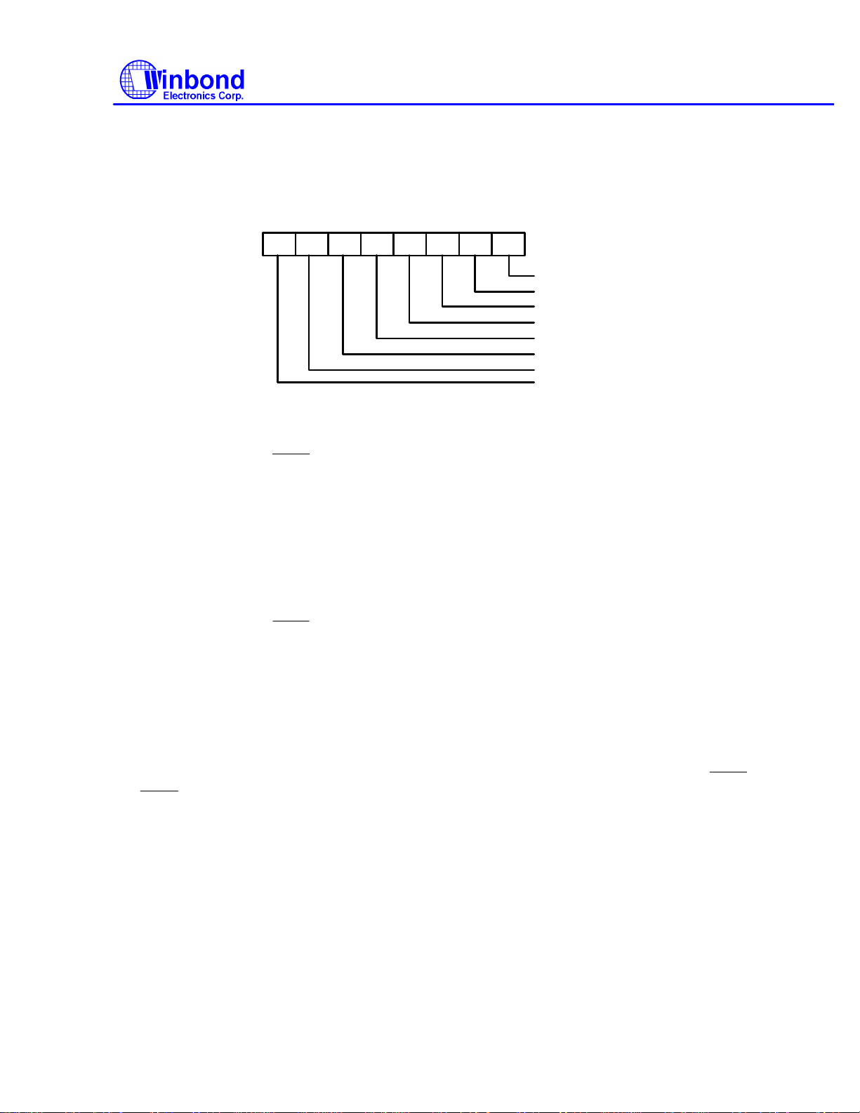
W83787IF
DTRB
RTSB
RTSA
DTRA
7.2.2 Configuration Register 1 (CR1) EFER = 89H, EFIR = 1H
When 89H is loaded into EFER and 01H is loaded into EFIR, the CR1 register can be accessed
through EFDR. The bit definitions are as follows:
7 6 5 4 3 2 1 0
URAS0
URBS0
URAS1
URBS1
PTRAS0
PTRAS1
Reserved
ABCHG
Notes:
URAS1 URAS0 (Bit 2, 0):
These two bits and URAS2 (CR3 bit 3) = 0 determine the base address of UARTA. (The default value
depends on SOUTA and
default.) When URAS2 = 1, see the description of CR3 bit 3.
00 Selects COM4 address, 2E8H
01 Selects COM3 address, 3E8H
10 Selects COM1 address, 3F8H
11 Disables UARTA port (when UARTA port is disabled, no clock will be input to this port
in order to save power)
at power-on setting. If there is no setting, UARTA is set to COM1 by
URBS1 URBS0 (Bit 3, 1):
These two bits and URBS2 (CR3 bit 2) = 0 determine the base address of UARTB. (The default value
depends on SOUTB and
default.) When URBS2 = 1, see the description of CR3 bit 2.
00 Selects COM3 address, 3E8H
01 Selects COM4 address, 2E8H
10 Selects COM2 address, 2F8H
11 Disables UARTB port (when UARTB port is disabled, no clock will be input to this port
in order to save power)
PTRAS1, PTRAS0 (Bit 5, 4):
These two bits determine the base address of the parallel port. (The default value depends on
and
at power-on setting. If there is no setting, the default is LPT1.)
00 Selects LPT3 address, 3BCH
01 Selects LPT2 address, 278H
10 Selects LPT1 address, 378H
11 Disables parallel port all function modes
at power-on setting. If there is no setting, UARTB is set to COM2 by
Publication ReleaseDate:Sep 1995
- 64 - Revision A1
Page 65
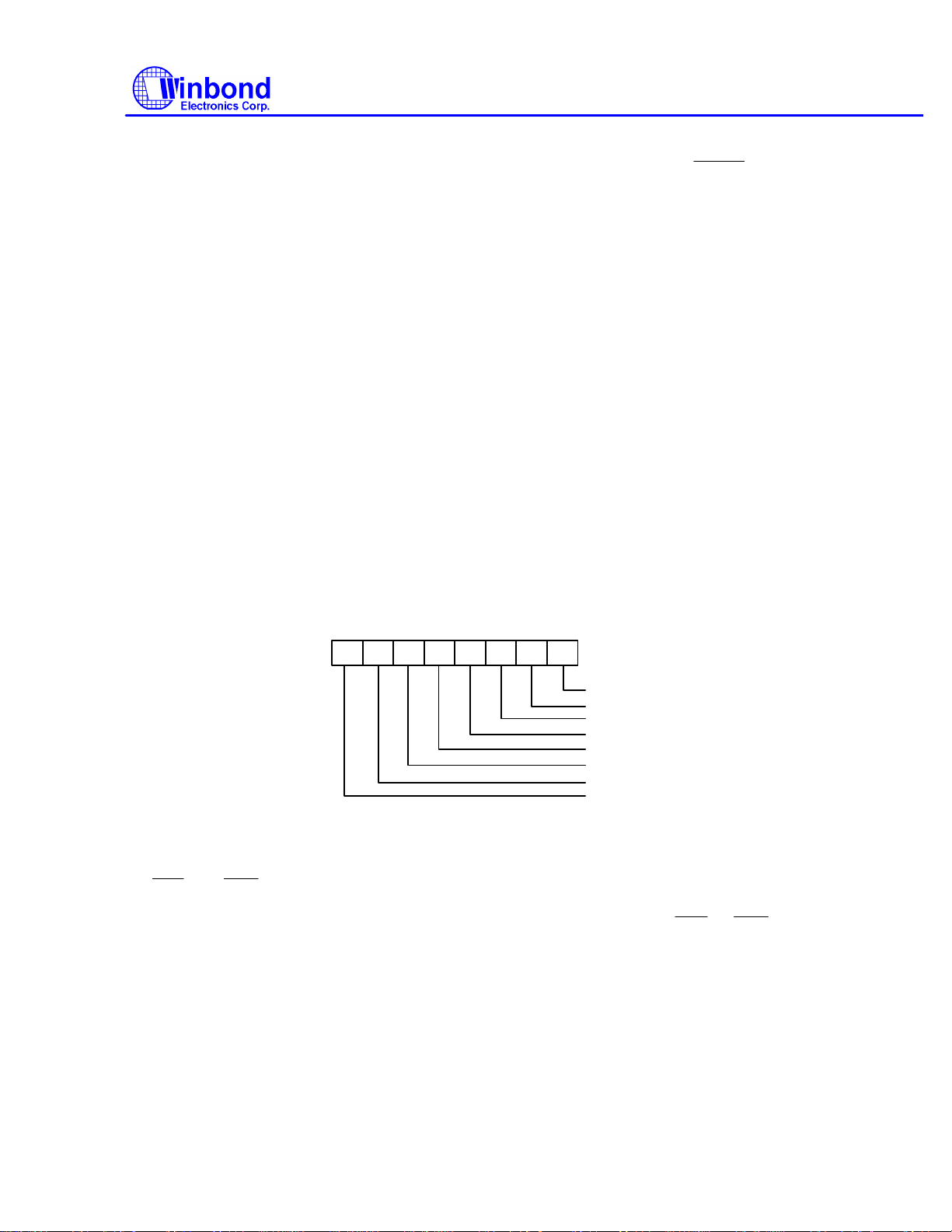
W83787IF
DBENL
XRD
XWR
XRD
XWR
ABCHG (Bit 7):
This bit enables the FDC AB Change Mode. (The default value depends on
power-on setting. If there is no setting, the default is normal mode.)
0 Drives A and B assigned as usual
1 Drive A and drive B assignments exchanged
Examples (debug instructions):
Example 7.4: Enable COM1 (3F8), COM2 (2F8), LPT1 (3BC); drives A and B assigned as in normal
operation.
Ex. 7.4
- O 250 89
- O 251 01
- O 252 0C
- O 250 00
Example 7.5: Enable only COM3 (3E8), LPT2 (278); assignments of drives A and B exchanged.
Ex. 7.5
- O 250 89
- O 251 01
- O 252 DB
- O 250 00
7.2.3 Configuration Register 2 (CR2) EFER = 89, EFIR = 2H
When EFER = 89H and EFIR = 02H, the CR2 register can be accessed through EFDR. The bit
definitions are as follows:
/ABCHG at
7 6 5 4 3 2 1 0
CEA
EA3
EA4
EA5
EA6
EA7
EA8
EA9
Notes:
When the W83787IF is programmed into extension adapter mode, the contents of this register are a
base address for the extension adapter. When base addresses EA3-EA9 are written into CR2, both
the
and
pins will be active low simultaneously and an adapter connected to the parallel
port can latch the same base address through pins XD1-XD7. After the base address is latched into
CR2, a subsequent read/write cycle to this same base address will generate an
or
signal.
If CEA is set to 0, then the W83787IF will compare system addresses SA9-SA3 with EA9-EA3 to
generate a compare-equal signal for this read/write command to access the Extension adapter. If
CEA is set to 1, then only EA9-EA4 are used in this comparison.
Publication ReleaseDate:Sep 1995
- 65 - Revision A1
Page 66
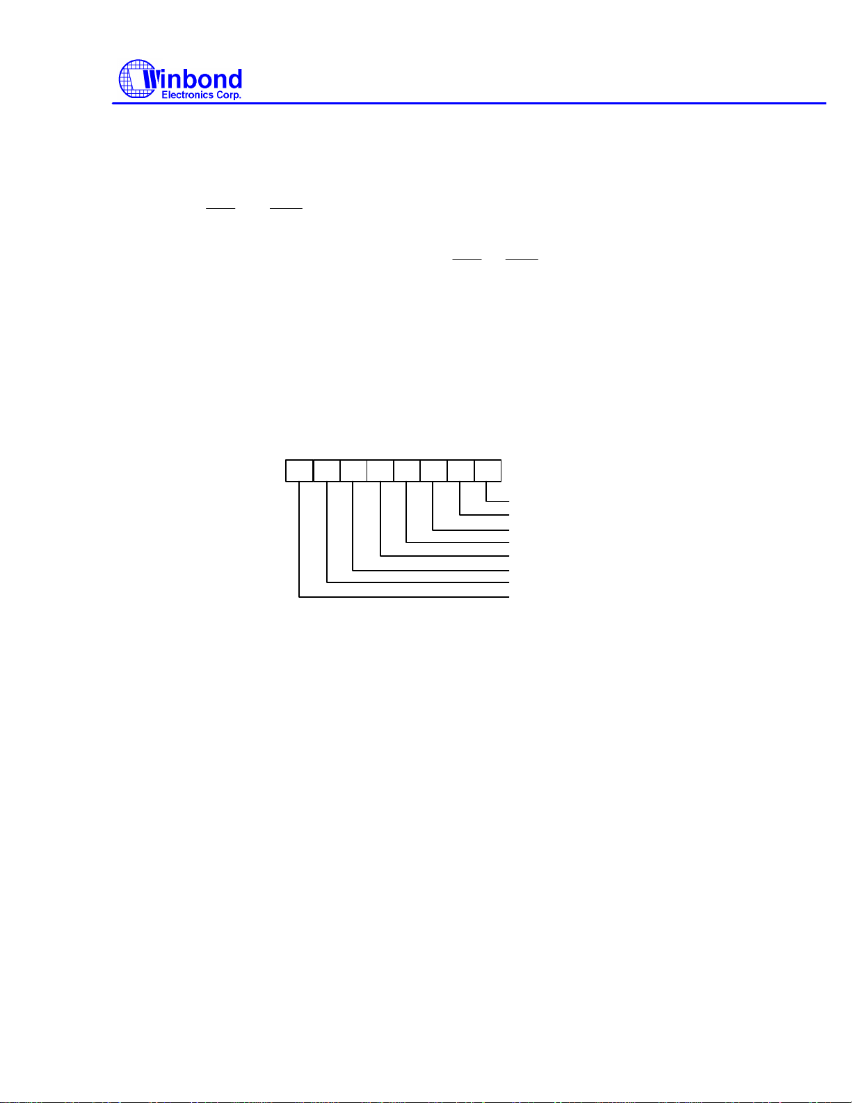
W83787IF
XRD
XWR
XRD
XWR
Examples (debug instructions):
Example 7.6: Enable IDE, FDC; enable extension adapter mode (assume I/O port is 300H).
- O 250 89
- O 251 00
- O 252 58 (Set Extension Adapter Mode)
- O 251 02 (
- O 252 C0 (Compare EA3-EA9)
- O 250 00
Example 7.7: Each time host reads/writes 300H-307H,
7.2.4 Configuration Register 3 (CR3) EFER = 89, EFIR = 3H
When 89H is loaded into EFER and 03H is loaded into EFIR, the CR3 register can be accessed
through EFDR. The bit definitions are as follows:
and
will be active low and C0H will appear at XD1- XD7)
or
is active.
In DMA cycles, IOR/W activates DACKX, which will also activate XRD or XWR
separately.
7 6 5 4 3 2 1 0
Notes:
SUBMIDI (Bit 0):
This bit selects the clock divide rate of UARTB.
0 disables MIDI support, UARTB clock = 24MHz divided by 13 (default)
1 enables MIDI support, UARTB clock = 24MHz divided by 12
SUAMIDI (Bit 1):
This bit selects the clock divide rate of UARTA.
0 Disables MIDI support, UARTA clock = 24MHz divided by 13 (default)
1 Enables MIDI support, UARTA clock = 24MHz divided by 12
URBS2 (Bit 2):
This bit determines the base address of UARTB.
0 Refer to the description of CR1 bit 1, 3
1 Selects COM1 address, 3F8H
URAS2 (bit 3):
This bit determines the base address of UARTA.
0 Refer to the description of CR1 bit 0, 2
1 Selects COM2 address, 2F8H
SUBMIDI
SUAMIDI
URBS2
URAS2
GMODS
EPPVER
GMENL
PRTBEN
Publication ReleaseDate:Sep 1995
- 66 - Revision A1
Page 67
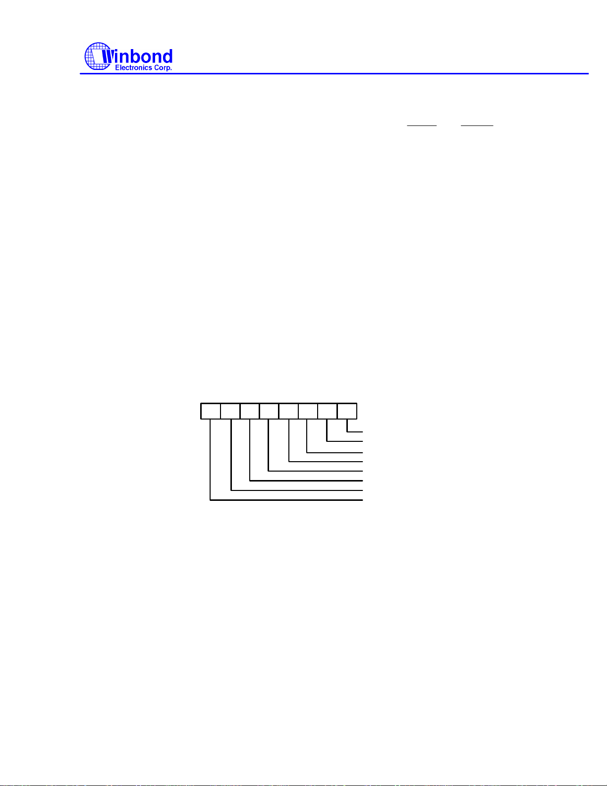
W83787IF
GMRD
GMWR
GMODS (Bit 4):
This bit selects the adapter mode or portable mode.
0 Selects the portable mode. Pins 41 and 39 will function as PFDCEN and PEXTEN
1 Selects the adapter mode. Pins 41 and 39 will function as
EPPVER (Bit 5):
This bit selects the EPP version of parallel port:
0 Selects the EPP 1.9 version
1 Selects the EPP 1.7 version (default)
GMENL (Bit 6):
This bit enables or disables game port.
0 Enables game port
1 Disables game port
PRTBEN (Bit 7):
This bit enables or disables the bi-directional capability of the parallel port in W83757 mode.
1 Disables the bi-directional capability of the parallel port
0 Enables the bi-directional capability of the parallel port. If the PRTOE pin is pulled
high or left floating, then the direction of the parallel port is controlled by bit 5 of the
printer control register (power-on default)
7.2.5 Configuration Register 4 (CR4) EFER = 89H, EFIR = 04H
When 89H is loaded into EFER and 04H is loaded into EFIR, the CR4 register can be accessed
through EFDR. The bit definitions are as follows:
and
Notes:
PRTPWD (Bit 7):
0 Supplies power to the parallel port
1 Puts the parallel port in power-down mode
GMPWD (Bit 6):
0 Supplies power to the game port
1 Puts the game port in power-down mode
URAPWD (Bit 5):
0 Supplies power to COMA
1 Puts COMA in power-down mode
URBPWD (Bit 4):
0 Supplies power to COMB
1 Puts COMB in power-down mode
7 6 5 4 3 2 1 0
URBTRI
URATRI
GMTRI
PRTTRI
URBPWD
URAPWD
GMPWD
PRTPWD
Publication ReleaseDate:Sep 1995
- 67 - Revision A1
Page 68
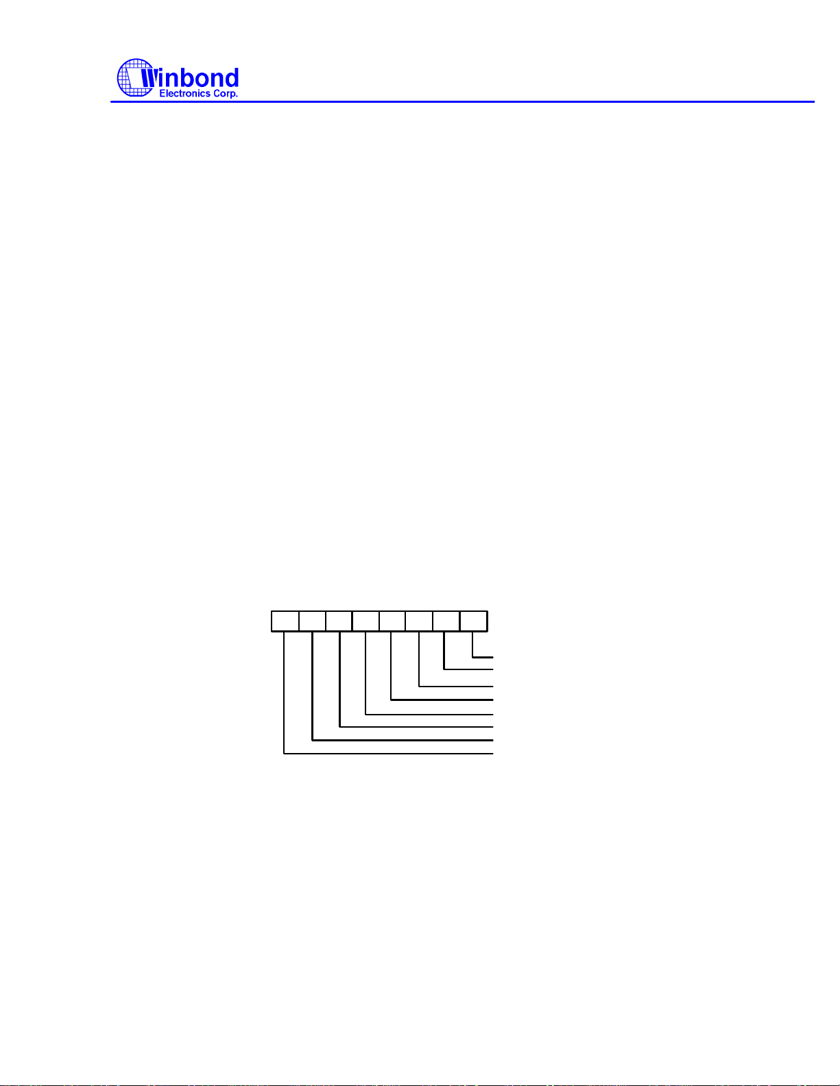
PRTTRI (Bit 3):
This bit enables or disables the tri-state outputs of parallel port in power-down mode.
0 The output pins of the parallel port will not be tri-stated when parallel port is in power-
down mode.
1 The output pins of the parallel port will be tri-stated when parallel port is in power-
down mode.
GMTRI (Bit 2):
This bit enables or disables the tri-state outputs of the game port in power-down mode.
0 The output pins of the game port will not be tri-stated when game port is in power-
down mode.
1 The output pins of the game port will be tri-stated when game port is in power-down
mode.
URATRI (Bit 1):
This bit enables or disables the tri-state outputs of UARTA in power-down mode.
0 The output pins of UARTA will not be tri-stated when UARTA is in power-down mode.
1 The output pins of UARTA will be tri-stated when UARTA is in power-down mode.
URBTRI (Bit 0):
This bit enables or disables the tri-state outputs of UARTB in power-down mode.
0 The output pins of UARTB will not be tri-stated when UARTB is in power-down mode.
1 The output pins of UARTB will be tri-stated when UARTB is in power-down mode.
W83787IF
7.2.6 Configuration Register 5 (CR5) EFER = 89H, EFIR = 05H
When 89H is loaded into EFER and 05H is loaded into EFIR, the CR5 register can be accessed
through EFDR. The bit definitions are as follows:
7 6 5 4 3 2 1 0
ECP FTHR0
ECP FTHR1
ECP FTHR2
ECP FTHR3
Reserved
Reserved
Reserved
Reserved
Notes:
Bit 7-4: Reserved
Bit 3-0: These four bits define the FIFO threshold for the ECP mode parallel port. The default value is
0000 after power-up.
7.2.7 Configuration Register 6 (CR6) EFER = 89H, EFIR = 06H
When 89H is loaded into EFER and 06H is loaded into EFIR, the CR6 register can be accessed
through EFDR. The bit definitions are as follows:
Publication ReleaseDate:Sep 1995
- 68 - Revision A1
Page 69
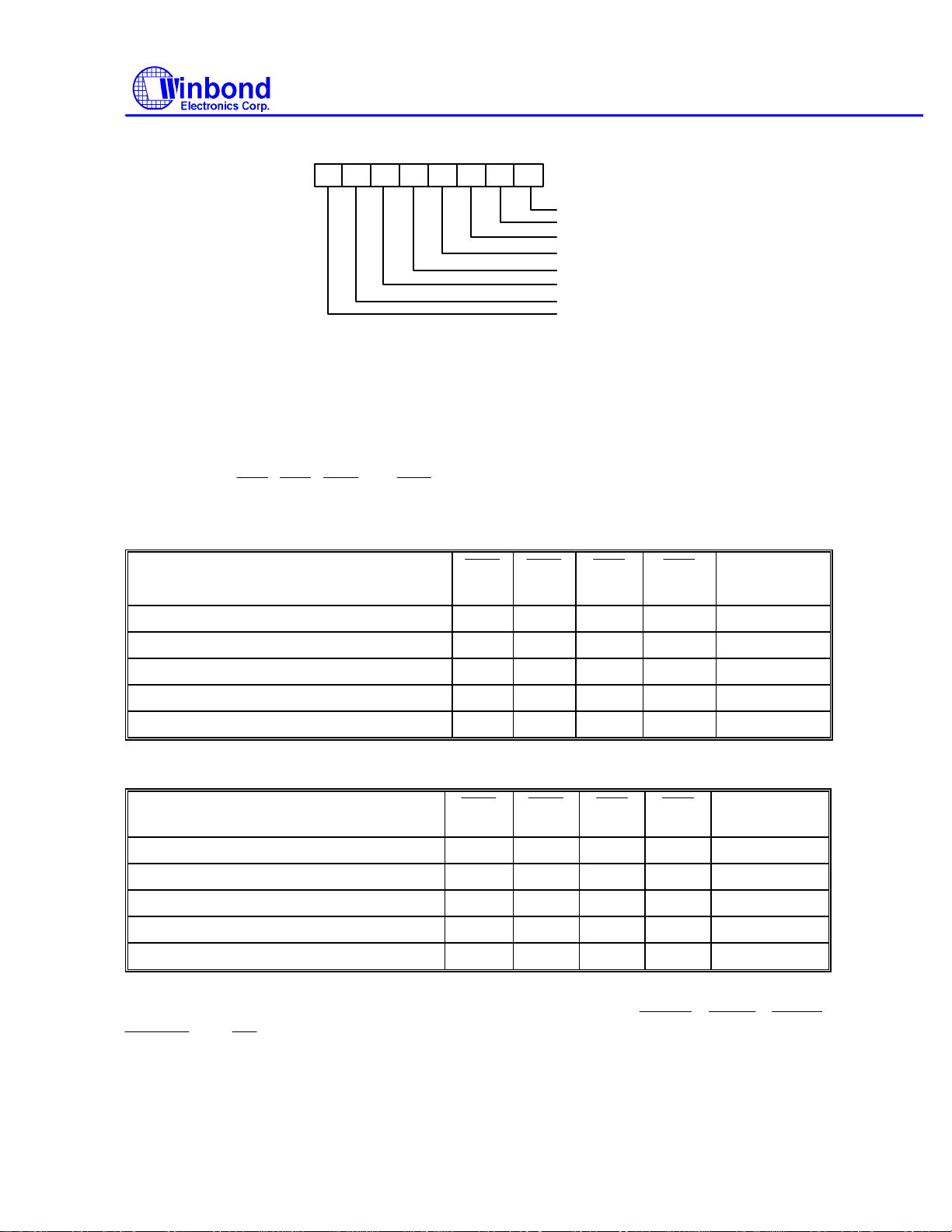
W83787IF
DSA
DSB
MOA
MOB
MOB
MOA
DSB
DSA
MOB
MOA
DSB
DSA
RDATA
INDEX
TRAK
0,DSKCHG
7 6 5 4 3 2 1 0
IDETRI
FDCTRI
IDEPWD
FDCPWD
FIPURDWM
SEL4FDD
OSCS2
Reserved
Bit 7: Reserved
OSCS2 (Bit 6): This bit and OSCS1, OSCS0 (bit 1, 0 of CR0) select one of the W83787IF's
power-down functions. Refer to descriptions of CR0.
SEL4FDD (Bit 5): Selects four FDD mode
0 Selects two FDD mode (see Table 7-2)
1 Selects four FDD mode
,
,
four drives.
Table 7-2
DO REGISTER ( 3F2H )
Bit 7 Bit 6 Bit 5 Bit 4 Bit 1 Bit 0
and
output pins are encoded as show in Table 7-3 to select
SELECTED
DRIVE
0 0 0 0 0 0 1 1 1 1 - 0 0 0 1 0 0 1 0 1 0 FDD A
0 0 1 0 0 1 0 1 0 1 FDD B
0 0 1 0 0 1 1 1 1 1 - 1 0 0 0 1 1 1 1 1 1 --
Table 7-3
DO REGISTER ( 3F2H )
Bit 7 Bit 6 Bit 5 Bit 4 Bit 1 Bit 0
DRIVE
SELECTED
0 0 0 0 x x 1 1 x x - 0 0 0 1 0 0 0 0 0 0 FDD A
0 0 1 0 0 1 0 0 0 1 FDD B
0 1 0 0 1 0 0 0 1 0 FDD C
1 0 0 0 1 1 0 0 1 1 FDD D
FIPURDWN (Bit 4):
This bit controls the internal pull-up resistors of the FDC input pins
,
,
, and WP.
0 The internal pull-up resistors of FDC are turned on.
1 The internal pull-up resistors of FDC are turned off.
Publication ReleaseDate:Sep 1995
- 69 - Revision A1
Page 70
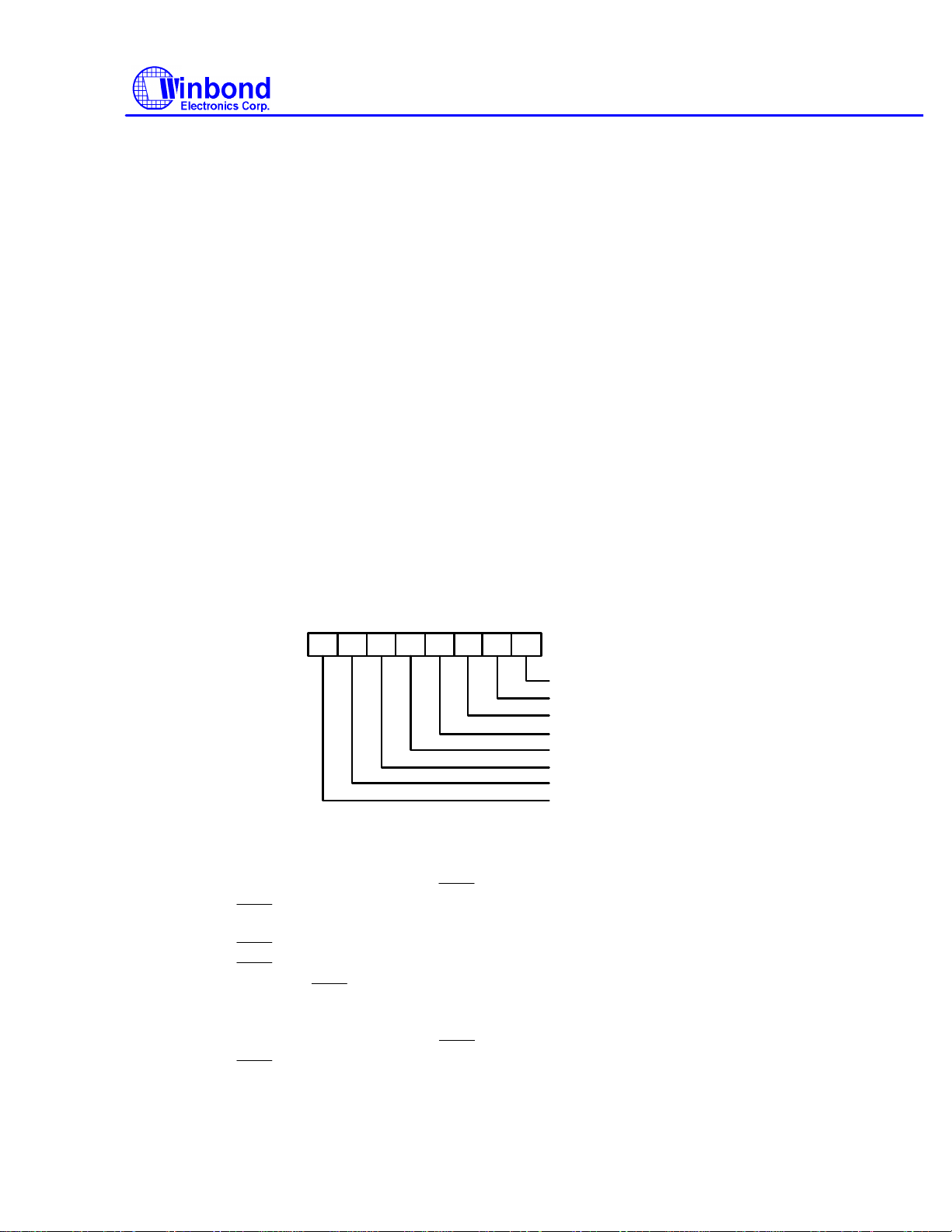
W83787IF
RWC
RWC
RWC
RWC
RWC
RWC
RWC
FDCPWD (Bit 3):
This bit controls the power to the FDC.
0 Power is supplied to the FDC.
1 Puts the FDC in power-down mode.
IDEPWD (Bit 2):
This bit controls the power of the IDE.
0 Power is supplied to the IDE.
1 Puts the IDE in power-down mode.
FDCTRI (Bit 1):
This bit enables or disables the tri-state outputs of the FDC in power-down mode.
0 The output pins of the FDC will not be tri-stated when FDC is in power-down mode.
1 The output pins of the FDC will be tri-stated when FDC is in power-down mode.
IDETRI (BIt 0):
This bit enables or disables the tri-state outputs of the IDE in power-down mode.
0 The output pins of the IDE will not be tri-stated when IDE is in power-down mode.
1 The output pins of the IDE will be tri-stated when IDE is in power-down mode.
7.2.8 Configuration Register 7 (CR7) EFER = 89H, EFIR = 07H
When 89H is loaded into EFER and 07H is loaded into EFIR, the CR7 register can be accessed
through EFDR. The bit definitions are as follows:
7 6 5 4 3 2 1 0
Notes:
FDD A type 1, 0 (Bit 1, 0):
These two bits select the type of FDD A.
00 Selects normal mode. When
= 1, the data transfer rate is 500 kb/s.
Three mode FDD select (EN3MODE = 1):
01
10
11 Don't care
= 0, selects 1.2 MB high-density FDD.
= 1, selects 1.44 MB high-density FDD.
, selects 720 KB double-density FDD.
FDD B type 1,0 (Bit 3,2):
These two bits select the type of FDD B.
00 Selects normal mode. When
= 1, the data transfer rate is 500 kb/s.
FDD A type 0
FDD A type 1
FDD B type 0
FDD B type 1
FDD C type 0
FDD C type 1
FDD D type 0
FDD D type 1
= 0, the data transfer rate is 250 kb/s. When
= 0, the data transfer rate is 250 kb/s. When
Publication ReleaseDate:Sep 1995
- 70 - Revision A1
Page 71
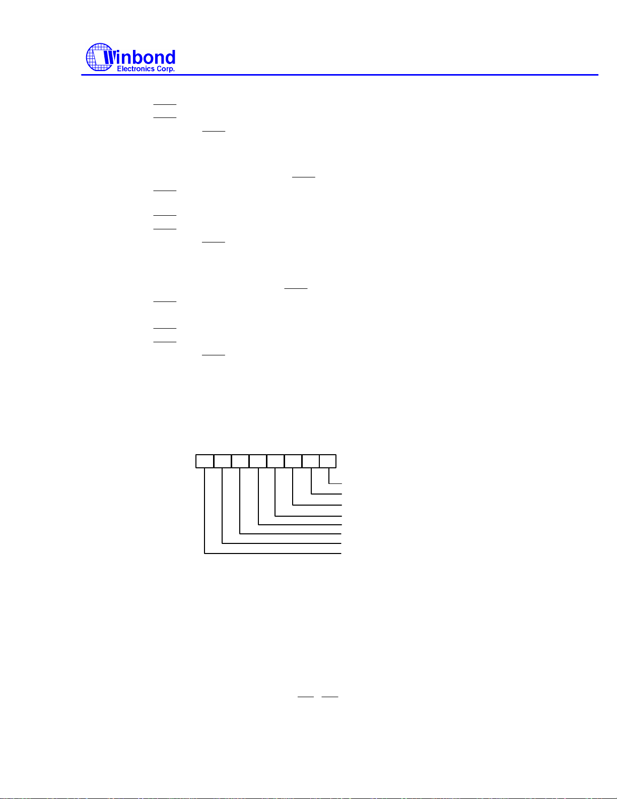
Three mode FDD select (EN3MODE = 1):
RWC
RWC
RWC
RWC
RWC
RWC
RWC
RWC
RWC
RWC
RWC
RWC
RWC
01
10
11 Don't care
= 0, selects 1.2 MB high-density FDD.
= 1, selects 1.44 MB high-density FDD.
, selects 720 KB double-density FDD.
FDD C type 1,0 (Bit 5,4):
These two bits select the type of FDD C.
00 Selects normal mode. When
= 1, he data transfer rate is 500 kb/s.
Three mode FDD select (EN 3 MODE = 1):
01
10
11 Don't care
= 0, selects 1.2 MB high-density FDD.
= 1, selects 1.44 MB high-density FDD.
, selects 720 KB double-density FDD.
FDD D type 1, 0 (Bit 7,6):
These two bits select the type of FDD D.
00 Selects normal mode. When
= 1, the data transfer rate is 500 kb/s.
Three mode FDD select (EN3MODE = 1):
01
10
11 Don't care
= 0, selects 1.2 MB high-density FDD.
= 1, selects 1.44 MB high-density FDD.
, selects 720 KB double-density FDD.
W83787IF
= 0, the data transfer rate is 250 kb/s. When
= 0, the data transfer rate is 250 kb/s. When
7.2.9 Configuration Register 8 (CR8) EFER = 89H, EFIR = 08H
When 89H is loaded into EFER and 08H is loaded into EFIR, the CR8 register can be accessed
through EFDR. The bit definitions are as follows:
7 6 5 4 3 2 1 0
Floppy Boot Drive 0
Floppy Boot Drive 1
Media ID 0
Media ID 1
SWWP
DISFDDWR
APDTMS2
APDTMS1
Notes:
APDTMS2 APDTMS1 (Bit 6, 7):
These two bits select the count-down time of the automatic power-down mode counter.
00 4 seconds
01 32 seconds
10 64 seconds
11 4 minutes
DISFDDWR (Bit 5):
This bit enables or disables FDD write data.
0 Enables FDD write
1 Disables FDD write (forces pins WE, WD to stay high)
Publication ReleaseDate:Sep 1995
- 71 - Revision A1
Page 72

W83787IF
WE
DSKCHG
Once this bit is set high, the FDC operates normally, but because pin
write data to diskettes. For example, if a diskette is formatted with DISFDDWR = 1, after the format
command has been executed, messages will be displayed that appear to indicate that the format is
complete. If the diskette is removed from the disk drive and inserted again, however, typing the DIR
command will reveal that the contents of the diskette have not been modified and the diskette was
not actually reformatted.
The reason for this is that as the operating system (e.g., DOS) reads the diskette files, it keeps the
files in memory. If there is a write operation, DOS will write data to the diskette and memory
simultaneously. When DOS wants to read the diskette, it will first search the files in memory. If DOS
finds the file in memory, it will not issue a read command to read the diskette. When DISFDDWR = 1,
DOS still writes data to the diskette and memory, but only the data in memory are updated. If a read
operation is performed, data are read from memory first, and not from the diskette. The action of
removing the diskette from the drive and inserting it again forces the
then read the contents of the diskette and will show that the contents have not been modified. The
same holds true with write commands.
The disable FDD write function allows users to protect diskettes against computer viruses by ensuring
that no data are written to the diskette.
SWWP (Bit 4):
0 Normal, use WP to determine whether the FDD is write-protected or not
1 FDD is always write-protected
Media ID 1 Media ID 0 (Bit 3, 2):
These two bits hold the media ID bit 1, 0 for three mode
is inactive, the FDD will not
pin active. DOS will
Floppy Boot Drive 1 Floppy Boot Drive 0 (bit 1, 0)
These two bits hold the value of floppy boot drive 1 and drive 0 for three mode
Publication ReleaseDate:Sep 1995
- 72 - Revision A1
Page 73
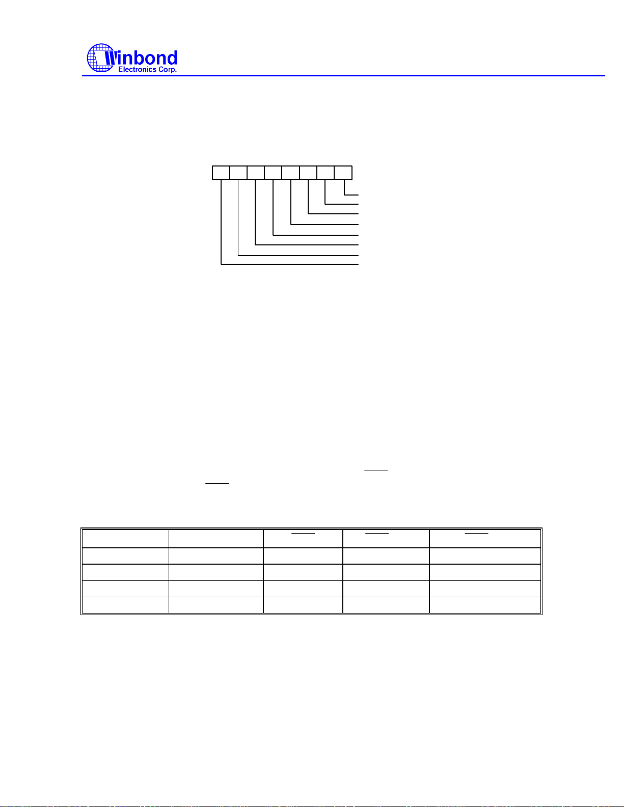
W83787IF
RWC
RWC
RWC
RWC
RWC
7.2.10 Configuration Register 9 (CR9) EFER = 89H, EFIR = 09H
When 89H is loaded into EFER and 09H is loaded into EFIR, the CR9 register can be accessed
through EFDR. The bit definitions are as follows:
7 6 5 4 3 2 1 0
CHIP ID0
CHIP ID1
CHIP ID2
CHIP ID3
Reserved
EN3MODE
LOCKREG
PRTMODS2
Notes:
PRTMODS2 (Bit 7):
This bit and PRTMODS1, PRTMODS0 (bits 3, 2 of CR0) select the operating mode of the W83787IF.
Refer to the descriptions of CR0.
LOCKREG (Bit 6):
This bit enables or disables the reading and writing of all configuration registers.
0 Enables the reading and writing of CR0-CRB
1 Disables the reading and writing of CR0-CRB (locks W83787IF extension
functions)
EN3MODE (Bit 5):
This bit enables or disables three mode FDD selection. When this bit is high, it enables the read/write
3F3H register.
0 Disables 3 mode FDD selection
1 Enables 3 mode FDD selection
When three mode FDD function is enabled, the value of
TDR(3F3H). The values of
and their meaning are shown in Table 7-4.
depends on bit 5 and bit 4 of
Table 7-4
BIT 5 OF TDR BIT 4 OF TDR
= 0
= 1
0 0 Normal 250K bps 500K bps
0 1 0 1.2 M FDD X
1 0 1 X 1.4M FDD
1 1 X X X
Bit 4: Reserved.
CHIP ID 3, CHIP ID 2, CHIP ID 1, CHIP ID 0 (Bit 3-0):
These four bits are read-only bits that contain chip identification information. The value is 9H for
W83787IF during a read.
Publication ReleaseDate:Sep 1995
- 73 - Revision A1
Page 74
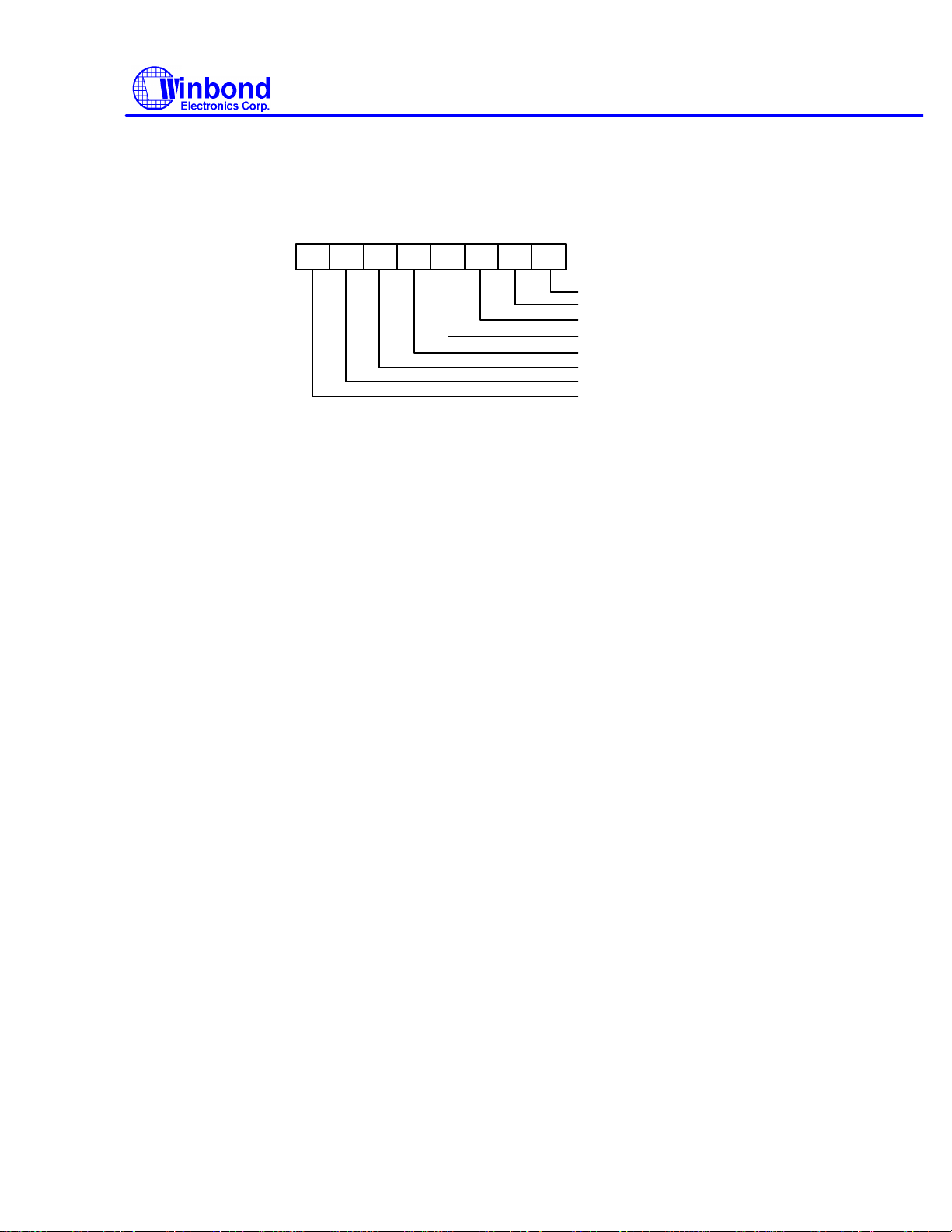
W83787IF
7.2.11 Configuration Register A (CRA) EFER = 89H, EFIR = 0AH
When 89H is loaded into EFER and 0AH is loaded into EFIR, the CRA register can be accessed
through EFDR. The bit definitions are as follows:
7 6 5 4 3 2 1 0
PEXTECPP
PEXT ECP
PEXT EPP
PEXT ADP
PDCACT
PDIRHOP
PEXT ACT
PFDCACT
Notes:
PFDCACT (Bit 7):
This bit controls whether PFDCEN (pin 41) is active high or low in portable mode.
0 PFDCEN is active low
1 PFDCEN is active high
PEXTACT (Bit 6):
This bit controls whether PEXTEN (pin 39) is active high or low in portable mode. This pin can also
reflect the mode of the parallel port: EXTADP mode, EPP mode, ECP mode, or ECP/EPP mode, or
any combination of these modes.
0 PEXTEN is active low
1 PEXTEN is active high
PDIRHOP (Bit 5):
This bit determines how the state of pin PDBDIR reflects (in all modes) whether the parallel port data
bus is input or output.
0 If PDBDIR is high, the parallel port data bus direction is input (read);
if PDBDIR is low, the parallel port data bus direction is output (write)
1 If PDBDIR is high, the parallel port data bus direction is output (write);
if PDBDIR is low, the parallel port data bus direction is input (read)
PDCACT (Bit 4):
This bit controls whether the PDCIN pin is active high or low.
0 PDCIN is active low
1 PDCIN is active high
PEXTADP (Bit 3):
This bit controls whether the PEXTEN pin is active in EXTADP mode.
0 PEXTEN is not active in EXTADP mode
1 PEXTEN is active in EXTADP mode
PEXTEPP (Bit 2):
This bit controls whether the PEXTEN pin is active in EPP mode.
0 PEXTEN is not active in EPP mode
1 PEXTEN is active in EPP mode
Publication ReleaseDate:Sep 1995
- 74 - Revision A1
Page 75

W83787IF
PEXTECP (Bit 1):
This bit controls whether the PEXTEN pin is active in ECP mode.
0 PEXTEN is not active in ECP mode
1 PEXTEN is active in ECP mode
PEXTECPP (Bit 0):
This bit controls whether the PEXTEN pin is active in ECP/EPP mode.
0 PEXTEN is not active in ECP/EPP mode
1 PEXTEN is active in ECP/EPP mode
7.2.12 Configuration Register B (CRB) EFER = 89H, EFIR = 0BH
This register is reserved.
7.2.13 Configuration Register C (CR0C) EFER = 89H, EFIR = 0CH (R/W)
When 89H is loaded into EFER and 0CH is loaded into EFIR, the CRC register can be accessed
through EFDR. The bit definitions are as follows:
7 6 5 4 3 2 1 0
TX2INV
RX2INV
IDEGIOSEL
URIRSEL
Reserved
HEFERE
TURB
TURA
Notes:
TURA (Bit 7):
This bit is represent the clcok source of UART A.
0 The clock source is 1.8462MHZ (24 MHZ divide 13). Hence, the maximum baud rate
of UART A is 115.2K bps. (Default)
1 The clock source is 24MHZ, that is, the maximum baud can be obtained 24/16 MHZ. This
can be used in loopback testing or higher data transfer.
TURB (Bit 6):
This bit is the clock source of UART B described as Bit7.
HEFERE (Bit5):
This bit is EFER enable value.
0 The Extended Function Enable Register (EFER) enable value is set to 88H.
1 The Extended Function Enable Register (EFER) enable value is set to 89H.
During power-on reset, the default vaule is set by the Pin 41 (GMRD#) pulled high or low. This pin is
internal pull-high.
Bit 4: Reserved
Publication ReleaseDate:Sep 1995
- 75 - Revision A1
Page 76
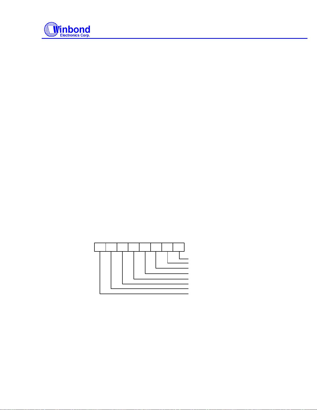
W83787IF
URIRSEL (Bit 3):
This bit select UART B operating in normal function or in IR function.
0 Select UART B as Infrared function.
1 Select UART B as normal function.
During power-on reset, the default value is set by Pin 92 (HURIRSEL) pulled high or low. This pin is
internal pull-high.
GIOSEL (Bit 2):
This bit select IDE function or GIO function.
0 Select the IDE pins definition compatible to W83787IF IDE pins definition.
1 Select the W83787IF IDE pins definition and general purpose I/O function.
During power-on reset, the default value is set by Pin 91 (HGIOSEL) pulled high or low. This pin is
pulled high internally.
RX2INV (Bit 1):
This bit is inverting or non-inverting the IR receiver data or SOUTB of UART B.
0 Non-inverting the SINB pin of UART B function or IRRX pin of IR function.
1 Inverting the SINB pin of UART B function or IRRX pin of IR function.
During the power-on reset, the default value is low.
TX2INV (Bit 0):
This bit is inverting or non-inverting IR transciever data or SINB of UART B.
0 Non-inverting the SINB pin of UART B or IRTX pin of IR function.
1 Inverting the SINB pin of UART B or IRTX pin of IR function.
During the power-on reset, the default value is low.
7.2.14 Configuration Register D (CR0D) EFER = 89H, EFIR = 0DH (R/W)
When 89H is loaded into EFER and 0DH is loaded into EFIR, the CR0D register can be accessed
through EFDR. The bit definitions are as follows:
7 6 5 4 3 2 1 0
IRMODE0
IRMODE1
IRMODE2
Half/Full Duplex
SIRRX0
SIRRX1
SIRTX0
SIRTX1
Notes:
SIRTX1 SIRTX0 (Bit 7, 6):
These two bits select IRTX pin in the IR function.
00 or 11 IRTX2 (Pin 2, PDBDIR)
01 IRTX1 (Pin 43, SOUTB)
10 IRTX3 (Pin 95, nCS1)
During the power-on reset, the default value is 00.
Publication ReleaseDate:Sep 1995
- 76 - Revision A1
Page 77
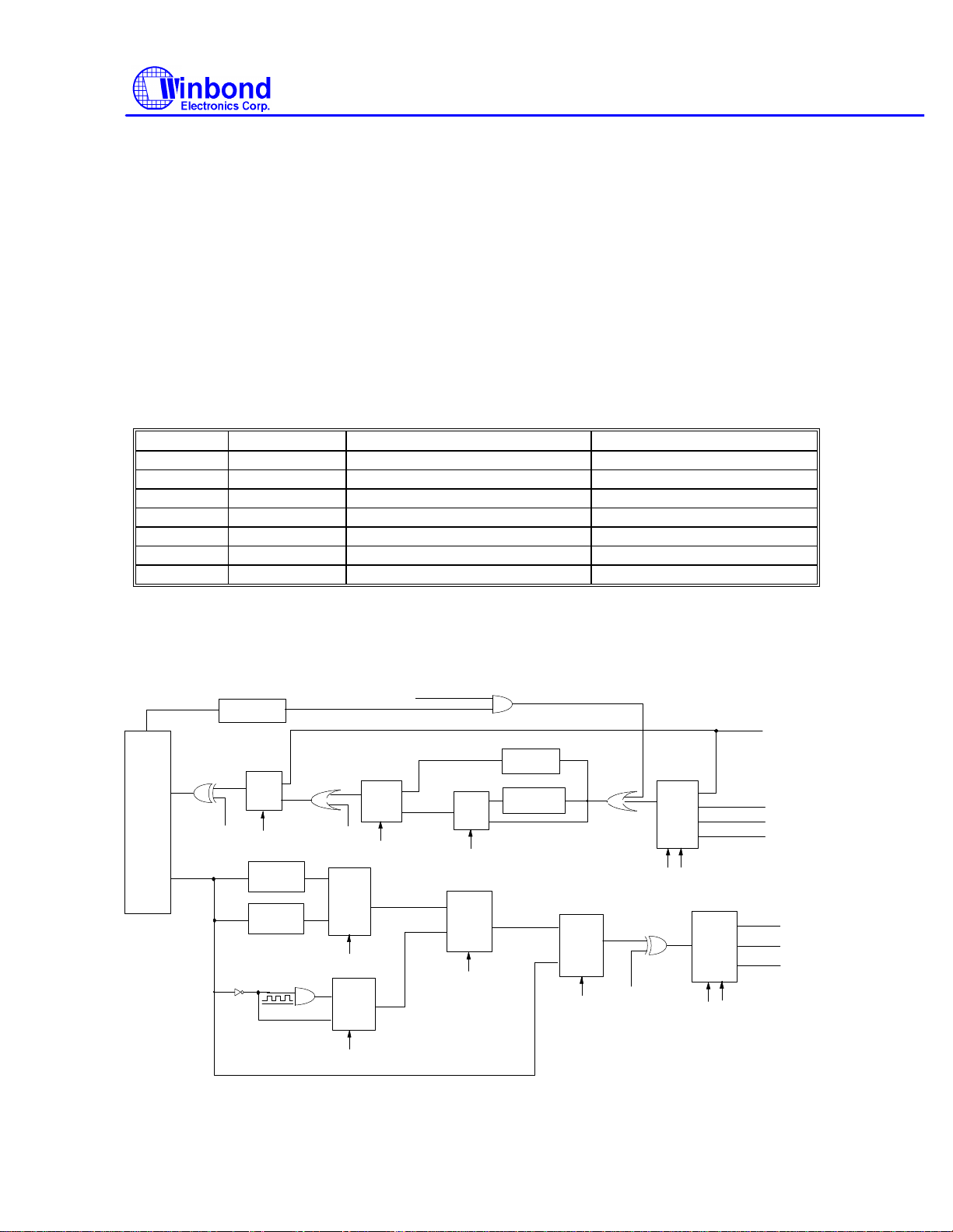
SIRRX1, SIRRX0 (Bit 5, 4):
These two bits select IRRX in the IR function.
00 IRRX2 (Pin 3, PDCIN)
01 IRRX1 (Pin 42, SINB)
10 IRRX4 (Pin 94, nCS0)
11 IRRX3 (Pin 1, nRESIDE)
During the power-on reset, the default value is 00..
Half/Full DUPLEX (Bit 3):
This bit select IR function operating in Half or Full Duplex mode.
0 The IR function is Full Duplex.
1 The IR function is Half Duplex.
IRMODE2, IRMODE1, IRMODE0 (Bit 2, 1, 0):
These three bits select IR operation mode.
IR MODE IR Function IRTX IRRX
00X Disable tri-state high
010* IrDA Active pulse 1.6 us Demodulation into SINB
011* IrDA Active pulse 3/16 bit time Demodulation into SINB
100 ASK-IR Inverting IRTX pin routed to SINB
101 ASK-IR Inverting IRTX & 500KHZ clock routed to SINB
110 ASK-IR Inverting IRTX Demodulation into SINB
111* ASK-IR Inverting IRTX & 500KHZ clock Demodulation into SINB
W83787IF
Note: The notation is normal mode in the IR function.
The SIR schematic diagram controlled the register CRC and CRD is shown as follows.
HUPLX
1
0
IRDA
(CRD.bit3)
IRMODE1
(CRD.bit1)
1 MUX
1
MUX 0
0
IRMODE2
(CRD.bit2)
Demodulation
IR-DA
Demodulation
ASK_IR
0
1 MUX
URIRSEL
(CRC,bit3)
TX2INV
CRC.bit0
01
00
10
11
MUX
SIRRX1~0
CR0D.bit5,4
SIRTX1~0
CRD.bit7,6
11,00
MUX
16550A
SIN
UART2
SOUT
Transmission
Time Frame
RX2INV
(CRC.bit1)
1
0
MUX
URIRSEL
(CRC.bit3)
IRDA Mod.
3/16
IRDA Mod.
Mod1.6u
500KHZ
IRMODE2,1=00
1
0 MUX
IRMODE0
(CRD.bit0)
1
0 MUX
IRMODE0
(CRD.bit0)
MUX
IRMODE2
(CRD.bit2)
IRRX1
IRRX2
IRRX4
IRRX3
01
10
IRTX2
IRTX1
IRTX3
SIN2
(default)
PDCIN
NCS0
NRSTIDE
(default)
PDBDIR
SOUT2
NCS1
Publication ReleaseDate:Sep 1995
- 77 - Revision A1
Page 78
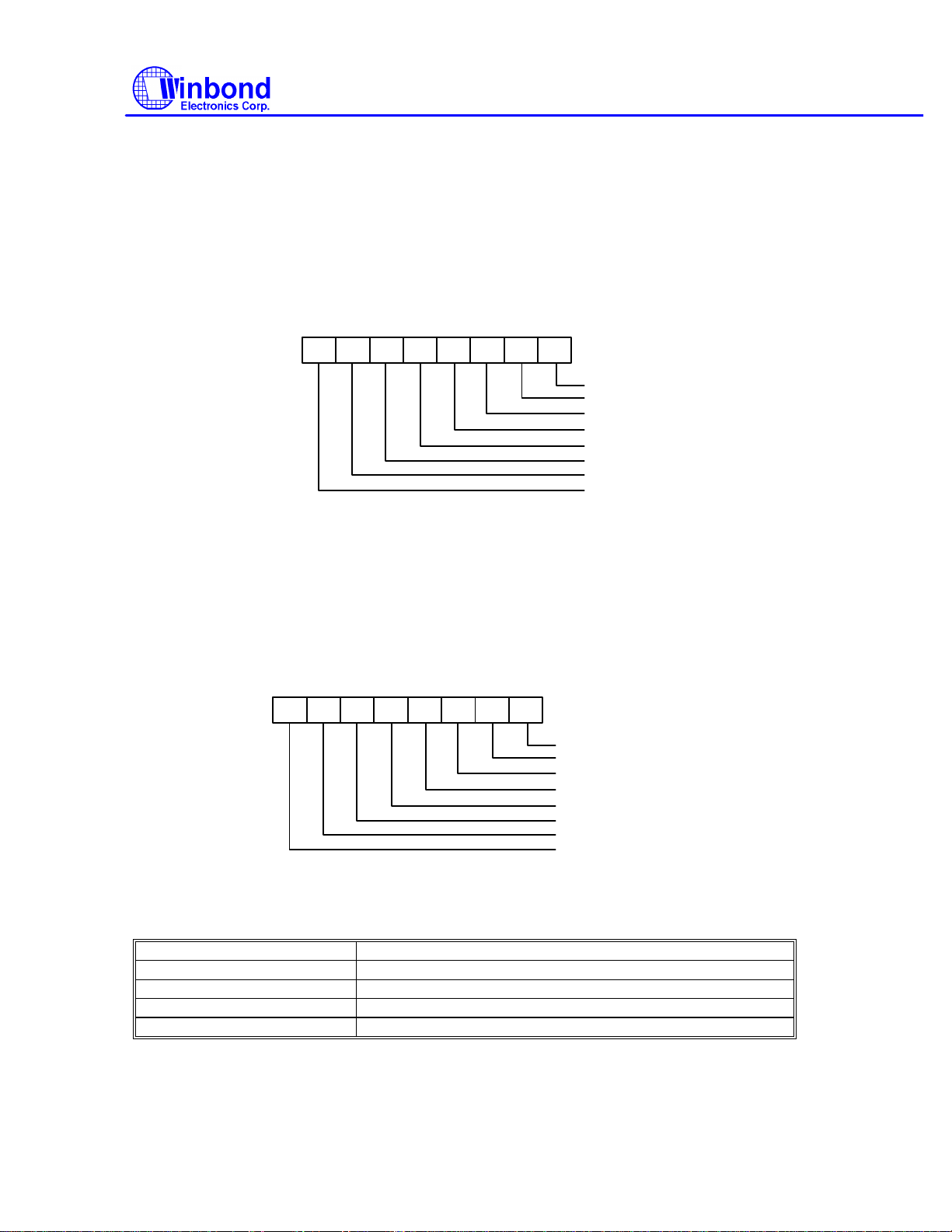
W83787IF
7.2.15 Configuration Register E, F (CR0E, CR0F) EFER = 89H, EFIR = 0EH, 0FH
Bit 7~ Bit 0: Reserved for testing.
7.2.16 Configuration Register 10H (CR10) EFER = 89H, EFIR = 10H (R/W)
When 89H is loaded into EFER and 10H is loaded into EFIR, the CR10 register can be accessed
through EFDR. The bit definitions are as follows:
7 6 5 4 3 2 1 0
GIO0AD0
GIO0AD1
GIO0AD2
GIO0AD3
GIO0AD4
GIO0AD5
GIO0AD6
GIO0AD7
Notes:
GIO0ADR7~0 (Bit 7 ~ Bit0):
These 8 bits select GIO0 (Pin 92) address bit 7 ~ bit 0, another GIO0 address bit 10 ~ bit 8 are
defined in CR11 bit 3 ~ bit 0.
7.2.17 Configuration Register 11H (CR11) EFER = 89H, EFIR = 11H (R/W)
When 89H is loaded into EFER and 11H is loaded into EFIR, the CR11 register can be accessed
through EFDR. The bit definitions are as follows:
7 6 5 4 3 2 1 0
GIO0AD8
GIO0AD9
GIO0AD10
Reserved
Reserved
Reserved
GIO0 ADR MODE0
GIO0 ADR MODE1
Notes:
GIO0 ADR MODE1 ~ 0 (Bit7 ~ Bit6):
These two bits select address mode. (Defined as following table)
GIO0 ADR MODE1 ~ 0 Decode Mode
00 1 byte decode (Compare GIO0ADR10~0 with SA10~0)
01 2 bytes decode (Compare GIO0ADR10~1 with SA10~1)
10 4 bytes decode (Compare GIO0ADR10~2 with SA10~2)
11 8 bytes decode (Compare GIO0ADR10~3 with SA10~3)
Bit 5 ~ Bit 3: Reserved.
Publication ReleaseDate:Sep 1995
- 78 - Revision A1
Page 79
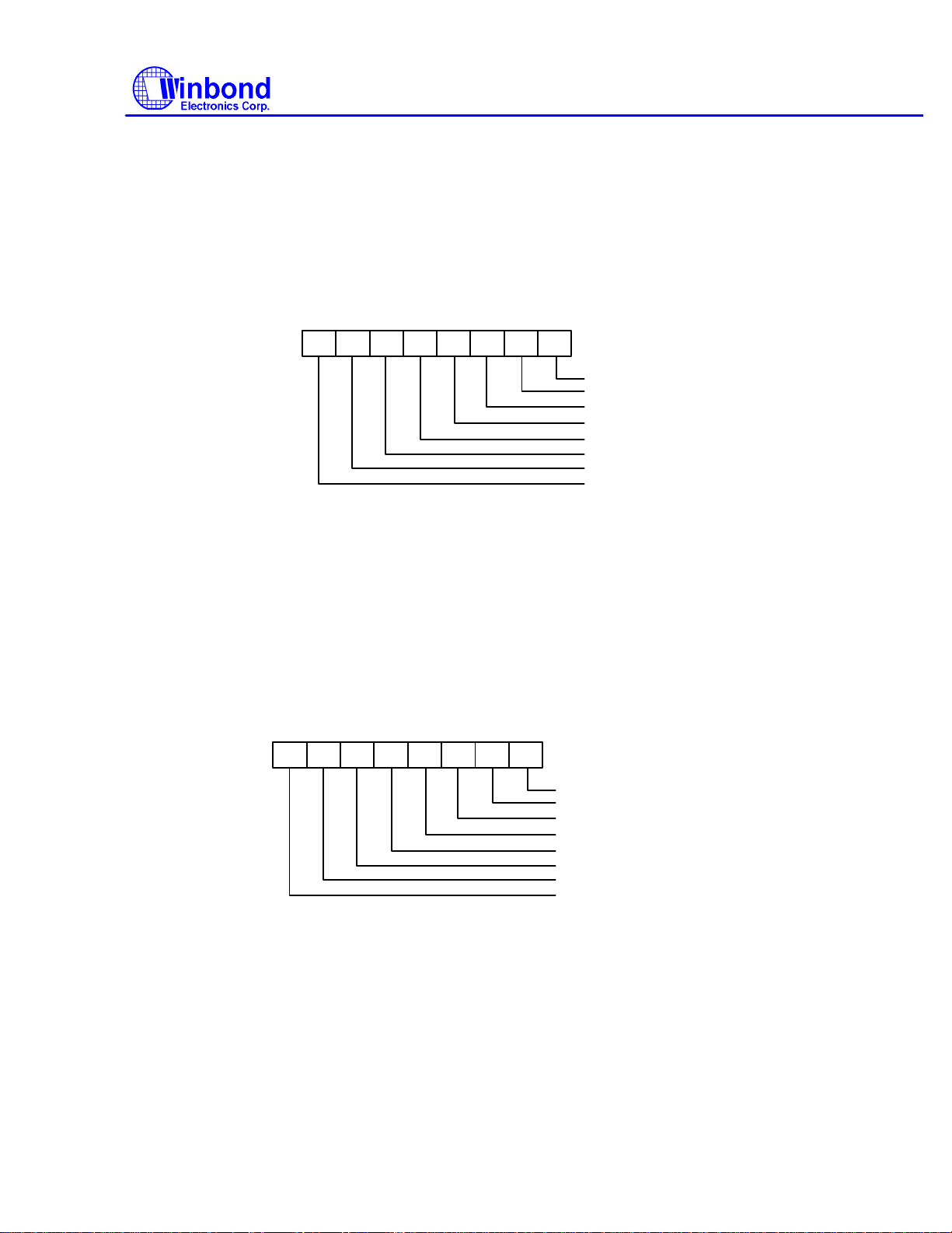
W83787IF
GIO0ADR10~8 (Bit 2 ~ Bit0):
These 3 bits select GIO0 address bit 10 ~ bit 8, another GIO0 address bit 7 ~ bit 0 are defined in
CR10 bit 7 ~ bit 0.
7.2.18 Configuration Register 12H (CR12) EFER = 89H, EFIR = 12H (R/W)
When 89H is loaded into EFER and 12H is loaded into EFIR, the CR12 register can be accessed
through EFDR. The bit definitions are as follows:
7 6 5 4 3 2 1 0
GIO1AD0
GIO1AD1
GIO1AD2
GIO1AD3
GIO1AD4
GIO1AD5
GIO1AD6
GIO1AD7
Notes:
GIO1ADR7~0 (Bit 7 ~ Bit0):
These 8 bits select GIO1 (Pin 96) address bit 7 ~ bit 0, another GIO1 address bit 10 ~ bit 8 are
defined in CR13 bit 3 ~ bit 0.
7.2.19 Configuration Register 13H (CR13) EFER = 89H, EFIR = 13H (R/W)
When 89H is loaded into EFER and 13H is loaded into EFIR, the CR13 register can be accessed
through EFDR. The bit definitions are as follows:
7 6 5 4 3 2 1 0
GIO1AD8
GIO1AD9
GIO1AD10
Reserved
Reserved
Reserved
GIO1 ADR MODE0
GIO1 ADR MODE1
Notes:
GIO1 ADR MODE1 ~ 0 (Bit7 ~ Bit6):
These two bits select address mode. (Defined as following table)
Publication ReleaseDate:Sep 1995
- 79 - Revision A1
Page 80
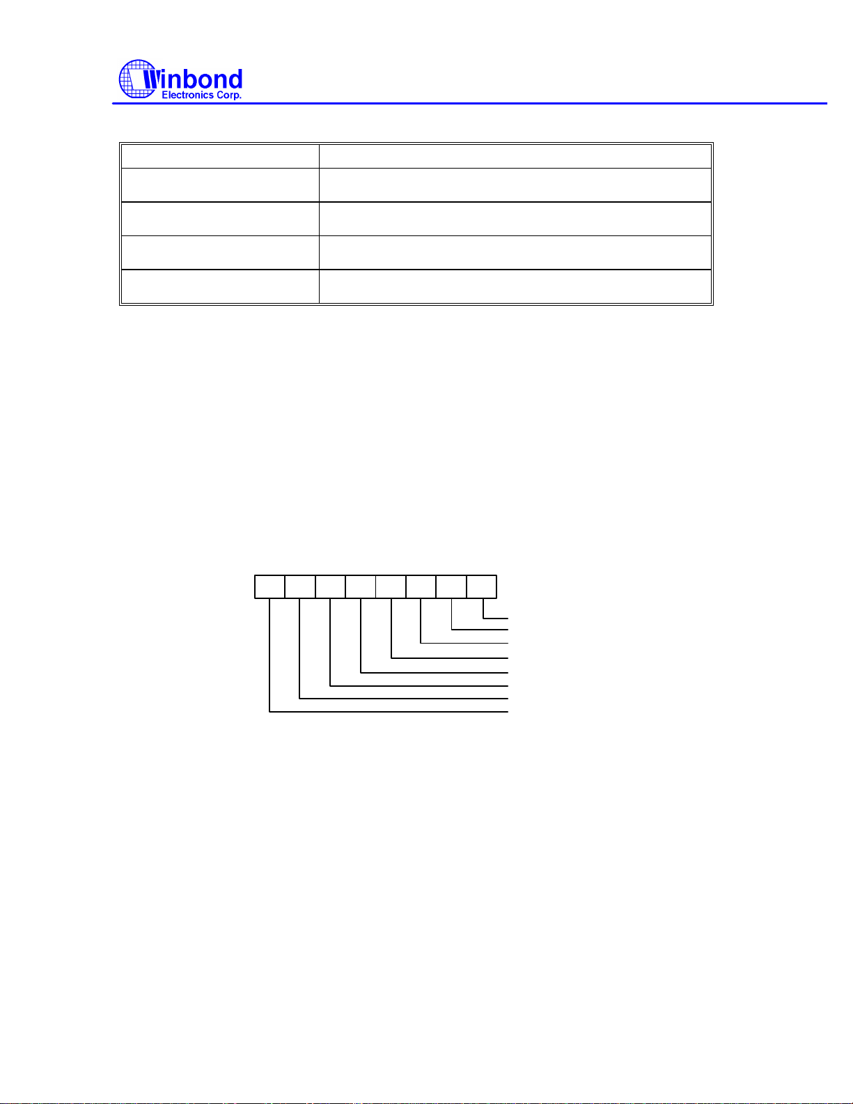
W83787IF
GIO1 ADR MODE1 ~ 0 Decode Mode
00 1 byte decode (Compare GIO1ADR10~0 with SA10~0)
01 2 bytes decode (Compare GIO1ADR10~1 with SA10~1)
10 4 bytes decode (Compare GIO1ADR10~2 with SA10~2)
11 8 bytes decode (Compare GIO1ADR10~3 with SA10~3)
Bit 5 ~ Bit 3: Reserved.
GIO1ADR10~8 (Bit 2 ~ Bit0):
These 3 bits select GIO1 address bit 10 ~ bit 8, another GIO1 address bit 7 ~ bit 0 are defined in
CR12 bit 7 ~ bit 0.
7.2.20 Configuration Register 14H (CR14) EFER = 89H, EFIR = 14H (R/W)
When 89H is loaded into EFER and 14H is loaded into EFIR, the CR14 register can be accessed
through EFDR. The bit definitions are as follows:
7 6 5 4 3 2 1 0
GDA0IPI
GDA0OPI
GCS0IOW
GCS0IOR
GIO0 CS TYPE
GIOP0MD0
GIOP0MD1
GIOP0MD2
Notes:
GIOP0MD2~0 (Bit 7 ~ Bit 5):
These three bits define GIO0 pin mode, that is either Chip-Select or Data Port, as shown in following
table.
Publication ReleaseDate:Sep 1995
- 80 - Revision A1
Page 81
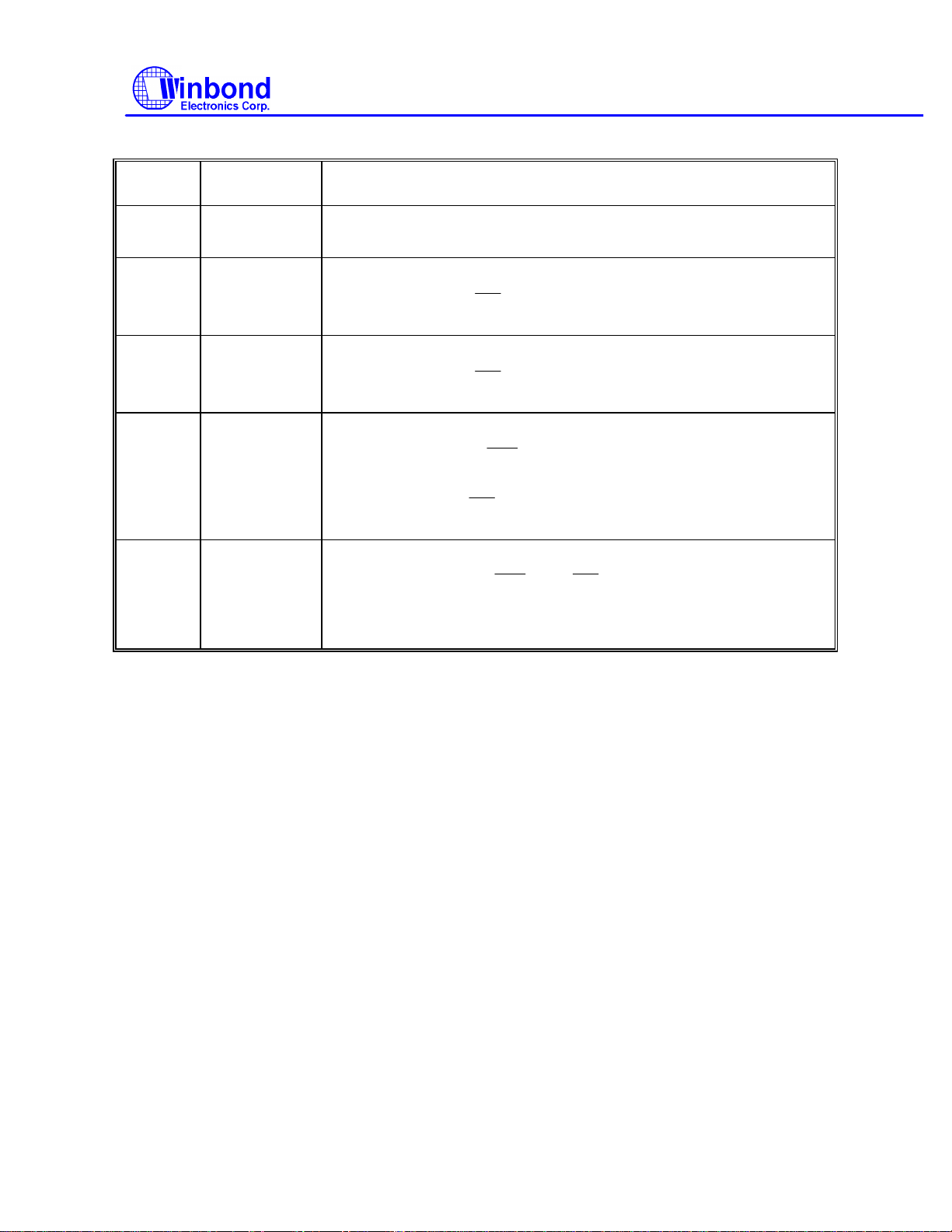
GIOP0MD2GIOP0MD1~0 GIOP0 Pin Mode
IOR
IOR
IOW
IOR
IOW
IOR
0 00 Inactive (tri-state)
W83787IF
0 01
0 10
0 11
1 XX
GIO0 CS TYPE (Bit 4):
This bit define the pin active state when GIOP0 acts as Chip Select pin.
0 Active LOW when (AEN=L) & (IOWN=L or IORN=L) & (SA10~0=GIO0AD10~0).
1 Active HIGH when (AEN=L) & (IOWN=L or IORN=L) & (SA10~0=GIO0AD10~0).
Data outport port (SD0→GIOP0).
When (AEN=L) & (
SD0 will present at GIOP0
Data input port (SD0←GIOP0).
When (AEN=L) & (
GIOP0 will present at SD0
Data I/O port (SD0↔GIOP0).
1. When (AEN=L) & (
SD0 will present at GIOP0, or
when (AEN=L)&(
GIOP0 will present at SD0
Chip Select Pin.
• When (AEN=L) & (
, the pin will be activated. The active level is defined in CR14.bit4
and the IORN or IOWN are defined in CR14.bit3~2.
=L) & (SA10~0=GIO0AD10~0), the value of
=L) & (SA10~0=GIO0AD10~0), the value of
=L) & (SA10~0=GIO0AD10~0), the value of
=L) &(SA10~0=GIO0AD10~0), the value of
=L or
=L) & (SA10~0=GIO0AD10~0)
GCS0IOR, GCS0IOW (Bit 3, Bit2):
These two bits define GIOP0 Chip Select Active Mode, that is in IORL, or IOWL, or IOR/WN, as
shown in the following table.
Publication ReleaseDate:Sep 1995
- 81 - Revision A1
Page 82
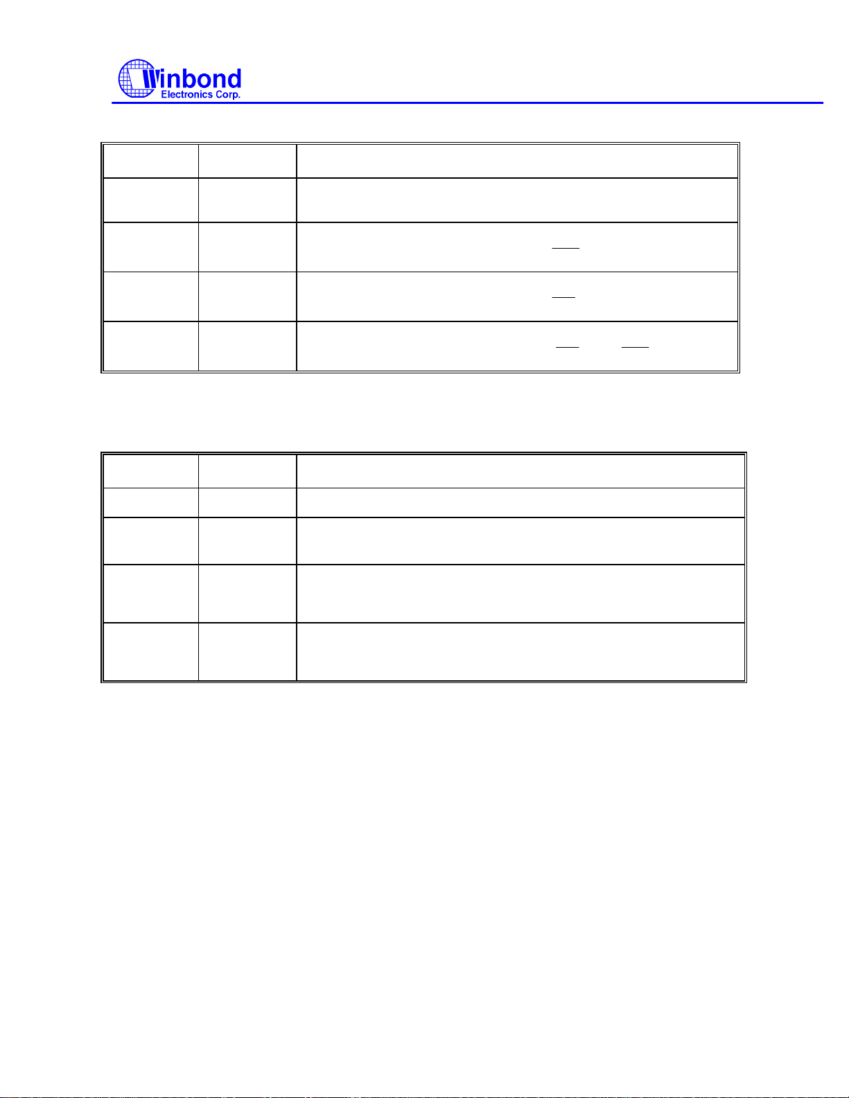
GCS0IOR GCS0IOW Chip Select Pin Type
IOW
IOR
IOR
IOW
0 0 The GIOP0 functions as a Chip select pin, and will active when
(AEN=L) & (SA10~0 = GIOAD10~0)
0 1 The GIOP0 functions as a Chip select pin, and will active when
(AEN=L) & (SA10~0 = GIOAD10~0) & (
1 0 The GIOP0 functions as a Chip select pin, and will active when
(AEN=L) & (SA10~0 = GIOAD10~0) & (
1 1 The GIOP0 functions as a Chip select pin, and will active when
(AEN=L) & (SA10~0 = GIOAD10~0) & (
GDA0OPI, FDA0IPI (Bit 1, Bit0):
These two bits define GIOP0 Data Pin type as shown in the following table.
GDA0OPI GDA0IPI GIOP0 Data Pin Type
=L)
=L)
=L or
W83787IF
=L)
0 0 The GIO0 function as a data pin, and GIOP0→SD0, SD0→GIOP0
0 1 The GIO0 function as a data pin, and inverse GIOP0→SD0,
SD0→GIOP0
1 0 The GIO0 function as a data pin, and GIOP0→SD0,
inverse SD0→GIOP0
1 1 The GIO0 function as a data pin, and inverse GIOP0→SD0,
inverse SD0→GIOP0
7.2.21 Configuration Register 15H (CR15) EFER = 89H, EFIR = 15H (R/W)
When 89H is loaded into EFER and 15H is loaded into EFIR, the CR15 register can be accessed
through EFDR. The bit definitions are as follows:
Publication ReleaseDate:Sep 1995
- 82 - Revision A1
Page 83
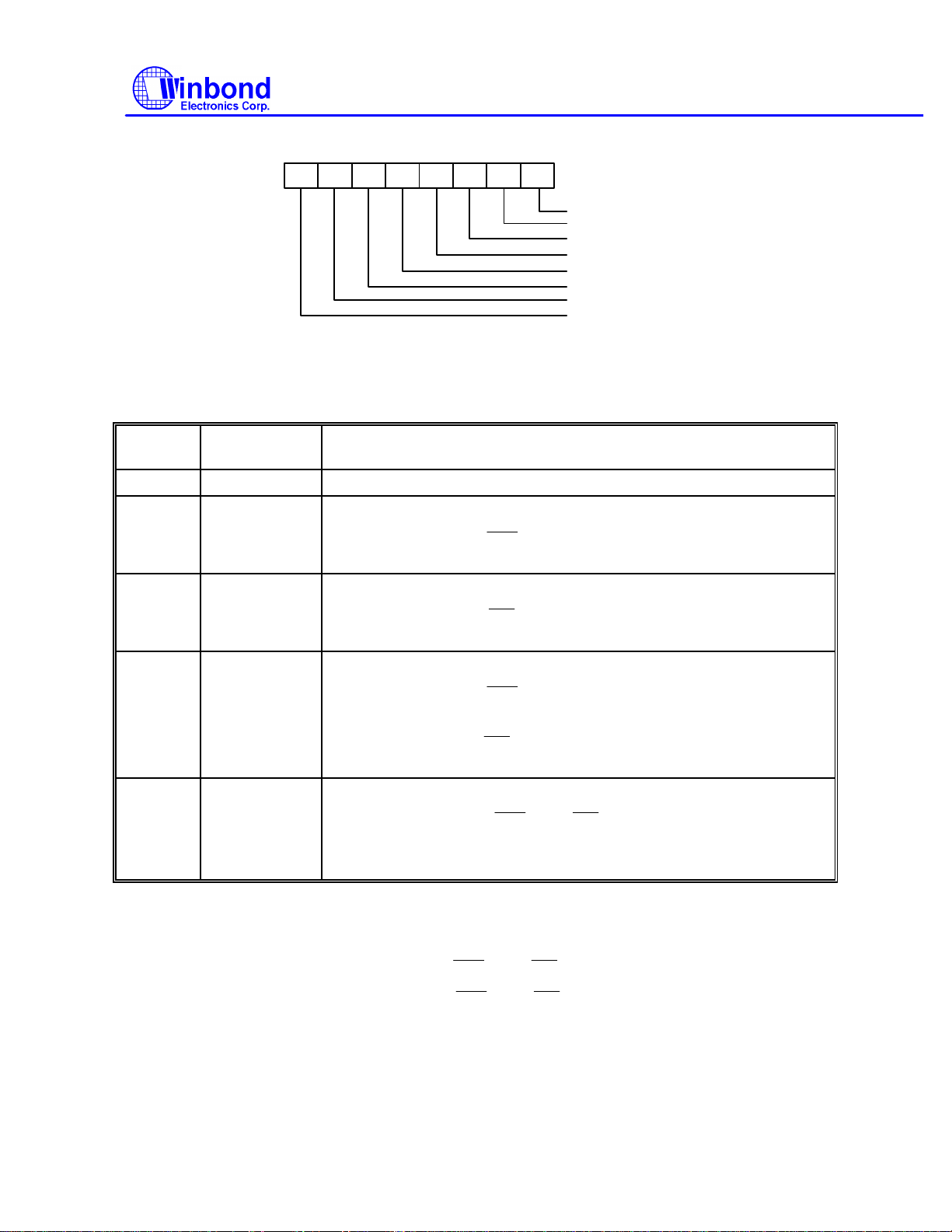
W83787IF
IOW
IOR
IOW
IOR
IOW
IOR
IOW
IOR
IOW
IOR
7 6 5 4 3 2 1 0
GDA1IPI
GDA1OPI
GCS1IOW
GCS1IOR
GIO1 CS TYPE
GIOP1MD0
GIOP1MD1
GIOP1MD2
Notes:
GIOP1MD2~0 (Bit 7 ~ Bit 5):
These three bits define GIOP1 pin mode, that is either Chip-Select or Data Port, as shown in
following table.
GIOP1MD2GIOP1MD1~0 GIO1 Pin Mode
0 00 Inactive (tri-state)
0 01
Data outport port (SDP0→GIOP0).
• When (AEN=L) & (
=L) & (SA10~0=GIO0AD10~0), the value of
SD0 will present at GIOP1
0 10
Data input port (SD0←GIOP0).
• When (AEN=L) & (
=L) & (SA10~0=GIO0AD10~0), the value of
GIOP1 will present at SD0
0 11
Data I/O port (SD0↔GIOP0).
1. When (AEN=L) & (
=L) & (SA10~0=GIO0AD10~0), the value of
SD0 will present at GIOP1, or
2. when (AEN=L)&(
=L) &(SA10~0=GIO0AD10~0), the value of
GIOP1 will present at SD0
1 XX
Chip Select Pin.
• When (AEN=L) & (
=L or
=L) & (SA10~0=GIO0AD10~0)
, the pin will be activated. The active level is defined in CR15.bit4
and the IORN or IOWN are defined in CR15.bit3~2.
GIO1 CS TYPE (Bit 4):
This bit define the pin active state when GIOP1 acts as Chip Select pin.
0 Active LOW when (AEN=L) & (
1 Active HIGH when (AEN=L) & (
=L or
=L or
=L) & (SA10~0=GIO0AD10~0).
=L) & (SA10~0=GIO0AD10~0).
Publication ReleaseDate:Sep 1995
- 83 - Revision A1
Page 84
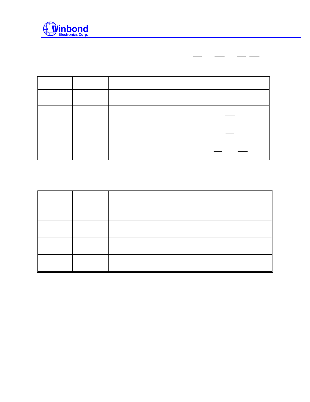
GCS1IOR, GCS1IOW (Bit 3, Bit2):
IOR
IOW
IOR/IOW
IOW
IOR
IOR
IOW
W83787IF
These two bits define GIO1 Chip Select Active Mode, that is in
shown in the following table.
GCS1IOR GCS1IOW Chip Select Pin Type
0 0 The GIOP1 function as a Chip select pin, and will active when
(AEN=L) & (SA10~0 = GIOAD10~0)
0 1 The GIOP1 function as a Chip select pin, and will active when
(AEN=L) & (SA10~0 = GIOAD10~0) & (
1 0 The GIOP1 function as a Chip select pin, and will active when
(AEN=L) & (SA10~0 = GIOAD10~0) & (
1 1 The GIOP1 function as a Chip select pin, and will active when
(AEN=L) & (SA10~0 = GIOAD10~0) & (
GDA1OPI, FDA1IPI (Bit 1, Bit0):
These two bits define GIO1 Data Pin type as shown in the following table.
GDA1OPI GDA1IPI GIOP1 Data Pin Type
, or
, or
=L or
, as
=L)
=L)
=L)
0 0 The GIOP1 functions as a data pin, and GIOP1→SD1,
SD1→GIOP1
0 1 The GIOP1 functions as a data pin, and inverse GIOP1→SD1,
SD1→GIOP1
1 0 The GIOP1 functions as a data pin, and GIOP1→SD1,
inverse SD1→GIOP1
1 1 The GIOP1 functions as a data pin, and inverse GIOP1→SD1,
inverse SD1→GIOP1
Publication ReleaseDate:Sep 1995
- 84 - Revision A1
Page 85
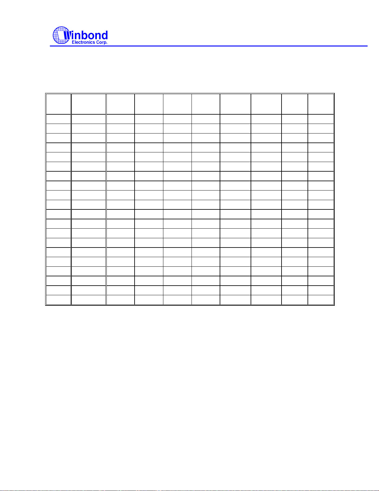
7.2.12 Bit Map Configuration Registers
Table 7-6
Power-on
Reg.
CR0 sss1 ss00
CR1 00ss ssss
CR2 0000 0000
CR3 0011 0000
CR4 0000 0000
CR5 0000 0000
CR6 0000 0000
CR7 0000 0000
CR8 0000 0000
CR9 s000 1001
CRA 0001 1111
CRB 0000 0000
CRC 00s0 ss00
CRD 0000 0011
CR10 0000 0000
CR11 0000 0000
CR12 0000 0000
CR13 0000 0000
CR14 0000 0000
CR15 0000 0000
Reset Value
(D7-D0)
D7
D6 D5 D4 D3 D2 D1 D0
IDEEN HADSEL FDCEN FADSEL
ABCHG 0 PRTAS1 PRTAS0 URBS1 URAS1 URBS0 URAS0
RA9 RA8 RA7 RA6 RA5 RA4 RA3 CEA
PRTBEN GMENL EPPVER GMODS URAS2 URBS2 SUAMIDI SUBMIDI
PRTPWD GMPWD URAPWD URBPWD PRTTRI GMTRI URATRI URBTRI
0 0 0 0 ECPTHR3 ECPTHR2
0 OSCS2 SEL4FDD FIPURDWN FDCPWD IDEPWD FDCTRI IDETRI
FDD D T1 FDD D T0 FDD C T1 FDD C T0 FDD B T1 FDD B T0
APDTMS1 APDTMS0
PRTMODS2
PFDCACT
LOCKREG EN3MODE
PEXTACT PDIRHISOP
0 0 0 0 0 0 0 0
TURA TURB HEFERE 0 URIRSEL GIOSEL RX2INV TX2INV
SIRTX1 SIRTX0 SIRRX1 SIRRX0 HDUPLX IRMODE2
GIO0AD7 GIO0AD6 GIO0AD5 GIO0AD4 GIO0AD3 GIO0AD2
G0CADM1 G0CADM0
GIO1AD7 GIO1AD6 GIO1AD5 GIO1AD4 GIO1AD3 GIO1AD2
G1CADM1 G1CADM0
GIOP0MD2 GIOP0MD1 GIOP0MD0
GIOP1MD2 GIOP1MD1 GIOP1MD0
W83787IF
PRTMODS1 PRTMODS0
DISFDDWR SWWP MEDIA 1 MEDIA 0 BOOT 1 BOOT 0
0 CHIP ID 3 CHIP ID 2
PDCHACT
0 0 0
0 0 0
GIO0CSH GCS0IOR
GIO1CSH GCS1IOR
PEXTADP PEXTEPP
GIO0AD10 GIO0AD9 GIO0AD8
GIO1AD10 GIO1AD9 GIO1AD8
GCS0IOW GDA0OPI
GCS1IOW GDA1OPI
APD IPD
ECPTHR1 ECPTHR0
FDD A T1 FDD A T0
CHIP ID 1 CHIP ID 0
PEXTECP PEXTECPP
IRMODE1 IRMODE0
GIO0AD1 GIO0AD0
GIO1AD1 GIO1AD0
GDA0IPI
GDA1IPI
Notes:
1. ' s' means dependent on power-on setting of pin.
8.0 SPECIFICATIONS
8.1 ABSOLUTE MAXIMUM RATINGS
Power Supply Voltage..........................................................................-0.3 to 7.0V
Input Voltage.......................................................................................VSS-0.3 to VDD+0.3V
Operating Temperature........................................................................ 0° C to+70° C
Storage Temperature...........................................................................-55° C to+150° C
Publication ReleaseDate:Sep 1995
- 85 - Revision A1
Page 86
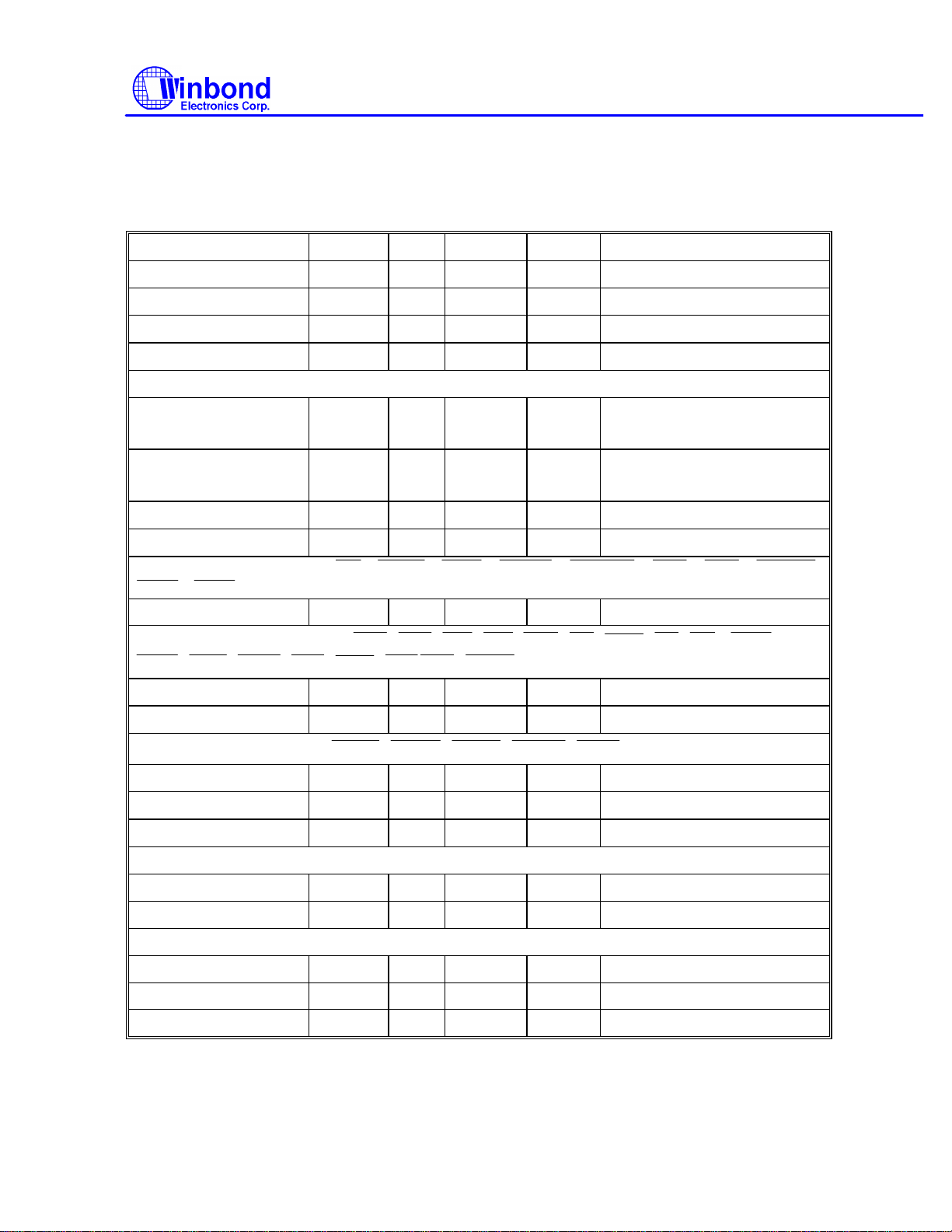
8.2 DC CHARACTERISTICS
INDEX
TRK
0, RDATA
DSKCHG
WP
2, IDX
2, TRAK
02
RDD
2
DCH
2
MOA
MOB
DSA, DSB, RWC
DIR
STEP
HEAD
MOB
2, DSB
2, RWC
2, DIR
2
STEP
WE2WD
2, HEAD
2
CS01
−, DBENH
DBENL
RESIDE
IDED
7
(Ta = 0° C to 70° C, VDD = 5V ± 5%, VSS = 0V)
PARAMETER SYM. MIN. MAX. UNIT CONDITIONS
Input Low Voltage VIL -0.3 0.8 V
Input High Voltage VIH 2.0 VDD+0.3 V
W83787IF
Input Leakage Current ILIH +10
Input Leakage Current ILIL -10
µS
µS
VIN = VDD
VIN = 0V
HOST INTERFACE PINS
Output Low Voltage VOL 0.4 V IOL = 12 mA (D0-D7)
4 mA (other pins)
Input High Voltage VOH 2.4 VDD V IOH = -12 mA (D0-D7)
4 mA (other pins)
Leakage Current ILOB 10
Leakage Current ILOB -10
DISK INTERFACE INPUT(WP,
,
)
,
µS
µS
,
VIN = VDD
VIN = 0V
,
Input Hysteresis VH 0.25 V
DISK INTERFACE OUTPUTS(
,
,
,
,
,
,
, WE, WD,
)
Output Low Voltage VOLD 0.4 V IOL = 24 mA
Leakage Current ILOH 10
IDE INTERFACE OUTPUT(
,
µS
,
,
VOUT = VDD
)
Output Low Voltage VOLD 0.4 V IOL = 4 mA
,
,
Leakage Current ILOH 10
Leakage Current ILOH -10
µS
µS
VOUT = VDD
UART, PARALLEL INTERFACE
Output Voltage VOL 0.4 V IOL = 4 mA on all outputs
VOH 2.4 VDD V IOH = -4 mA on all outputs
EXTENSION ADAPTER INTERFACE
Output Low Voltage VOL 0.4 V IOL = 12 mA
Output High Voltage VOHB 2.4 VDD V IOH = -12 mA
VDD Supply Current IDD 20 mA
Publication ReleaseDate:Sep 1995
- 86 - Revision A1
Page 87
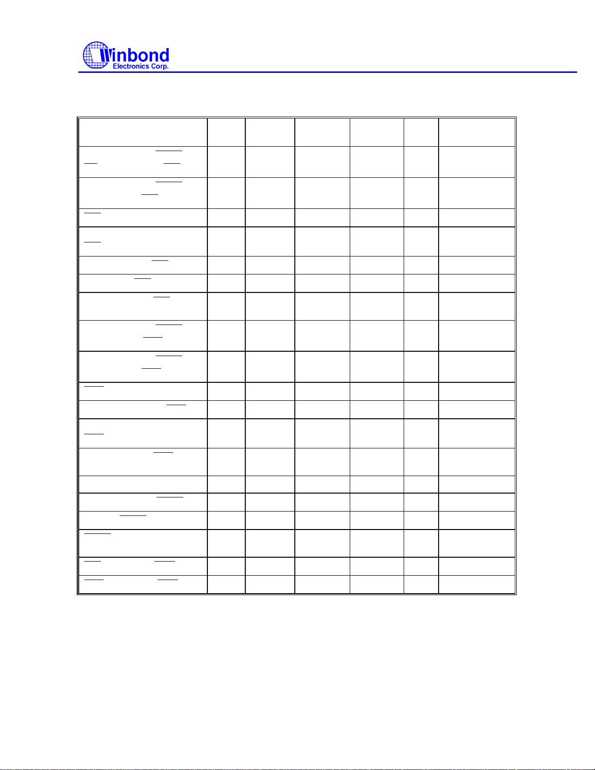
8.3 AC Characteristics
DACK
CS
IOR
DACK
IOR
IOR
IOR
IOR
IOR
IOR
DACK
IOW
DACK
IOW
IOW
IOW
IOW
IOW
DACK
DACK
DACK
IOR
DRQ
IOW
DRQ
8.3.1 FDC: Data rate = 500Kb/300Kb/250Kb/sec
PARAMETER SYM. MIN. TYP.
(NOTE 1)
W83787IF
MAX. UNIT TEST
CONDITIONS
SA9-SA0, AEN,
, setup time to
SA9-SA0, AEN,
hold time for
width
Data access time from
¡õ
Data hold from
SD to from
IRQ delay from
SA9-SA0, AEN,
setup time to
SA9-SA0, AEN,
hold time for
width
Data setup time to
Data hold time from
¡ô
¡ô
¡õ
¡ô
¡ô
¡õ
¡ô
¡õ
,
,
,
,
¡ô
TAR 25 nS
TAR 0 nS
TRR 80 nS
TFD 80 nS
TDH 10 nS
TDF 10 50 nS
TRI 360/570
/675
TAW 25 nS
TWA 0 nS
TWW 60 nS
TDW 60 nS
TWD 0 nS
nS
CL = 100 pf
CL = 100 pf
CL = 100 pf
IRQ delay from
DRQ cycle time TMCY 27
DRQ delay time
DRQ to
width
delay from
delay from
¡ô
¡õ
delay
TWI 360/570
TAM 50 nS
TMA 0 nS
TAA 260/430
/510
TMR 0 nS
TMW 0 nS
nS
/675
µS
nS
Publication ReleaseDate:Sep 1995
- 87 - Revision A1
Page 88
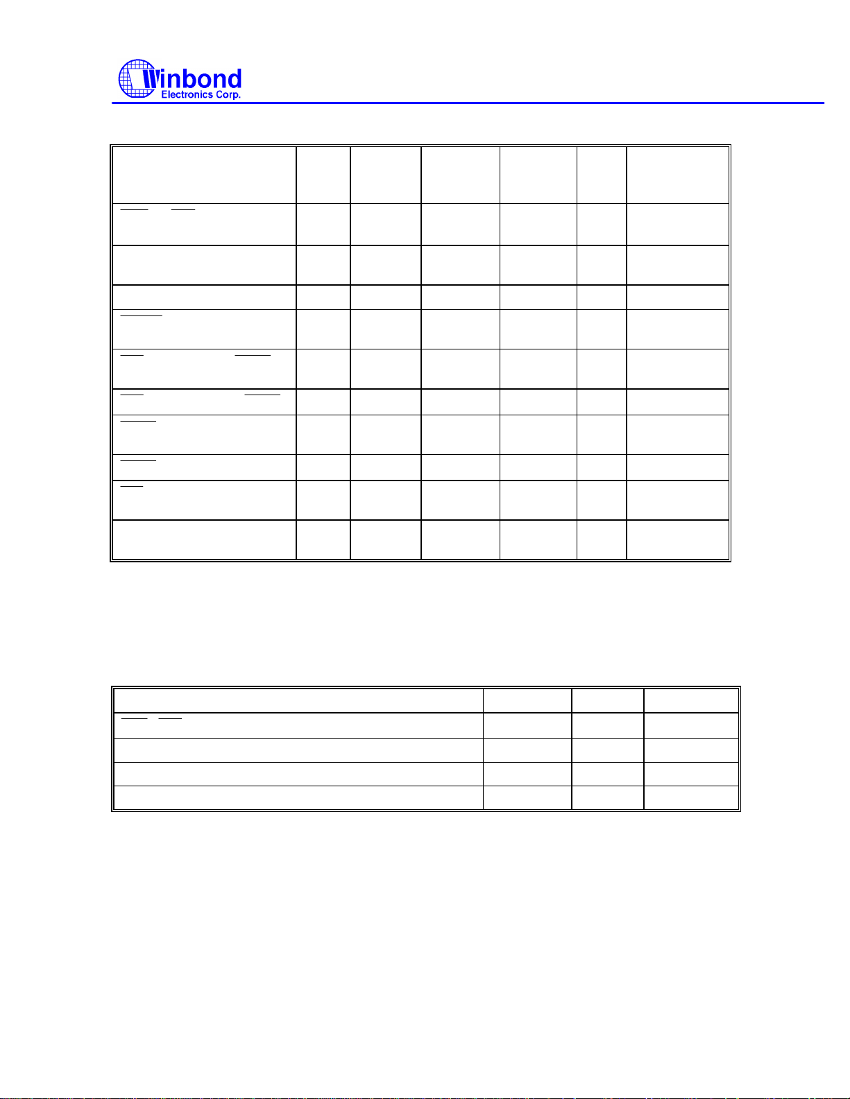
8.3 AC Characteristics, FDC continued
IOW
IOR
INDEX
DIR
STEP
DIR
STEP
STEP
STEP
WD
CS
0, CS
1
PARAMETER SYM. MIN. TYP.
(NOTE 1)
W83787IF
MAX. UNIT TEST
CONDITION
S
or
response time
TMRW 6/12
from DRQ
TC width TTC 135/220
/260
RESET width TRST 1.8/3/3.5
width
TIDX 0.5/0.9
/1.0
setup time to
TDST 1.0/1.6
/2.0
hold time from
pulse width
TSTD 24/40/48
TSTP 6.8/11.5
/13.8
cycle width
pulse width
TSC Note 2 Note 2 Note 2
TWDD 100/185
125/210
/225
Write precompensation TWPC 100/138
125/210
/225
Notes:
1. Typical values for T = 25° C and normal supply voltage.
2. Programmable from 2 mS through 32 mS in 2 mS increments.
/20/24
7/11.7
/14
/250
/250
7.2/11.9
/14.2
150/235
/275
150/235
/275
µS
nS
µS
µS
µS
µS
µS
µS
µS
µS
8.3.2 IDE
PARAMETER SYMBOL MAX. UNIT
delay from SA valid
T1 50 nS
DBENL, DBENH delay from AEN, IOCS16, SA T2 50 nS
IDED7 to D7 delay (read cycle) T4 50 nS
D7 to IDED7 delay (write cycle) T3 50 nS
Publication ReleaseDate:Sep 1995
- 88 - Revision A1
Page 89
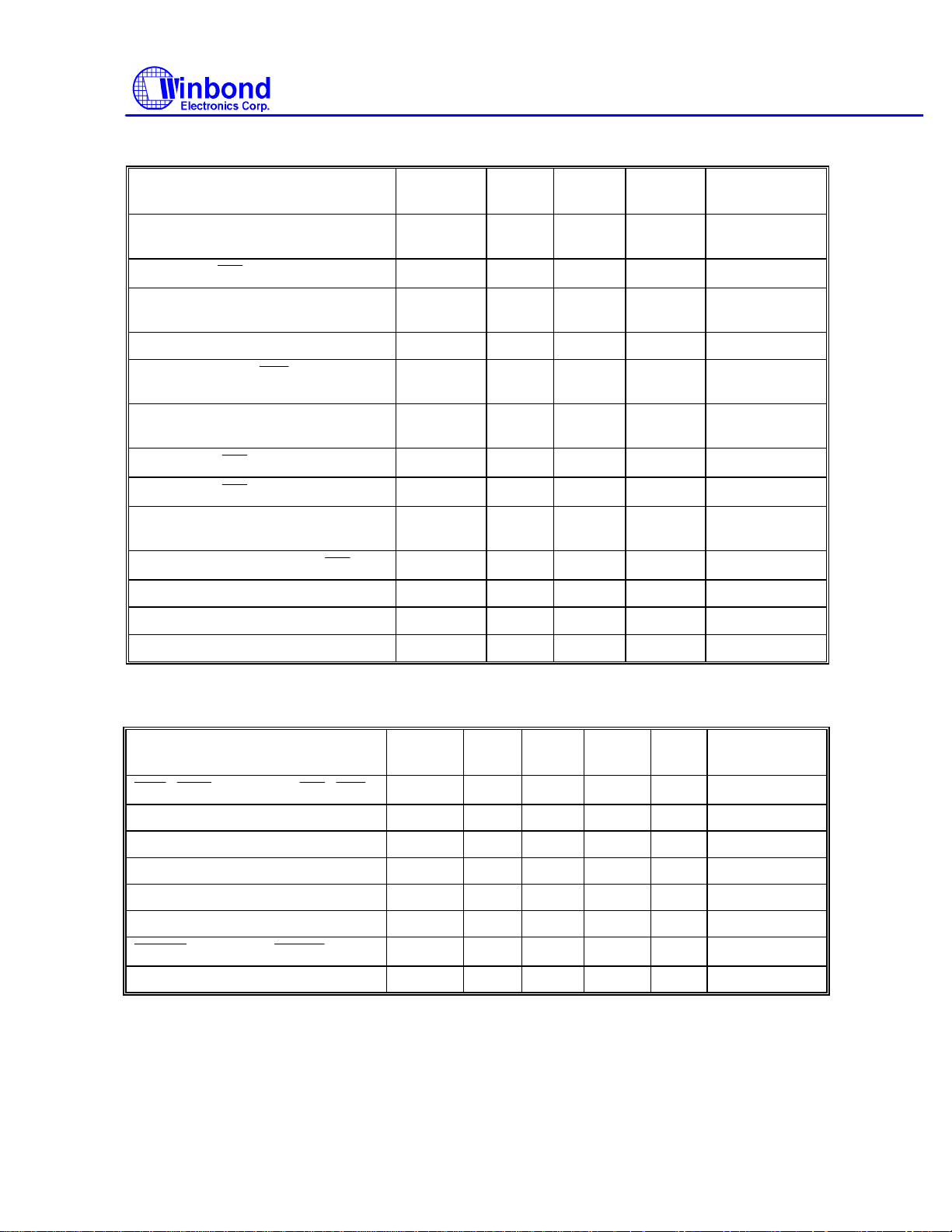
8.3.3 UART/Parallel Port
IOR
IOW
IOR
IOR
IOR
XRD
XWR
IOR, IOW
XDACK
DACKX
PARAMETER SYMBOL MIN. MAX. UNIT TEST
Delay from Stop to Set Interrupt TSINT 9/16 Baud
W83787IF
CONDITIONS
Rate
Delay from
Reset Interrupt
Delay from Initial IRQ Reset to
Transmit Start
TRINT 1
µS
TIRS 1/16 8/16 Baud
Rate
100pF Loading
Delay from to Reset interrupt THR 175 nS 100pF Loading
Delay from Initial
to interrupt
TSI 9/16 16/16 Baud
Rate
Delay from Stop to Set Interrupt TSTI 1/2 Baud
Rate
Delay from
Delay from
to Reset Interrupt
to Output
Set Interrupt Delay from Modem
TIR 250 nS 100pF Loading
TMWO 200 nS 100pF Loading
TSIM 250 nS
Input
Reset Interrupt Delay from
TRIM 250 nS
Interrupt Active Delay TIAD 25 nS 100pF Loading
Interrupt Inactive Delay TIID 30 nS 100pF Loading
Baud Divisor
N
216-1
100pF Loading
8.3.4 Extension Adapter Mode
PARAMETER SYM. MIN. TYP. MAX. UNIT TEST
,
Delay from
tx1 50 nS
XA<0:2> Delay from SA<0:2> tx2 50 nS
XD<0:7> Setup time tx3 50 nS
XD<0:7> Hold time tx4 0 nS
IRQ & Delay from XIRQ tx5 50 nS
DRQX Delay from XDRQ tx6 50 nS
Delay from
tx7 50 nS
XTC Delay from TC tx8 50 nS
Publication ReleaseDate:Sep 1995
- 89 - Revision A1
CONDITIONS
Page 90
W83787IF
INDEX
STROBE
AUTOFD
IOW
ACK
IOW
ERROR
IOR
IOR
IOR
IOR
IOW
IOR
IOR
IOR
WAIT
WRITE
IOR
WAIT
WRITE
WAIT
WRITE
IOR
WAIT
WAIT
WRITE
8.3.5 Parallel Port Mode Parameters
PARAMETER SYM. MIN. TYP. MAX. UNIT
PD0-7,
IRQ Delay from
IRQ Delay from
IRQ Active Low in ECP and EPP Modes t4 200 300 nS
8.3.6 EPP Data or Address Read Cycle Timing Parameters
Ax Valid to
IOCHRDY Deasserted to
Deasserted to Ax Valid
Deasserted to
Asserted to IOCHRDY Asserted
PD Valid to SD Valid t6 0 75 nS
Deasserted to SD Hi-Z (Hold Time)
SD Valid to IOCHRDY Deasserted t8 0 85 nS
Deasserted to IOCHRDY Deasserted
PD Hi-Z to PDBIR Set t10 0 nS
Deasserted to
Asserted to
Deasserted to
Asserted to PD Hi-Z
Asserted to PD Hi-Z
Command Asserted to PD Valid t18 0 nS
Command Deasserted to PD Hi-Z t19 0 nS
Deasserted to PD Drive
Deasserted to Command
,
Active to IRQ Active
Asserted
,
, nFAULT
PARAMETER SYM. MIN. MAX. UNIT
or
Asserted
Deasserted
Delay from
Deasserted
Asserted
Modified
t1 100 nS
t2 60 nS
t3 105 nS
t5 105 nS
t1 40 nS
t2 0 nS
t3 10 10 nS
t4 40
t5 0 24 nS
t7 0 40
t9 60 160 nS
t13 0 nS
t14 0 185 nS
t15 60 190 nS
t16 0 50 nS
t17 60 180 nS
t20 60 190 nS
t21 1 nS
µS
Publication ReleaseDate:Sep 1995
- 90 - Revision A1
Page 91
W83787IF
WAIT
WAIT
WAIT
WAIT
IOW
IOW
IOW
WAIT
WAIT
IOW
IOW
IOR
IOW
WAIT
IOW
WAIT
WRITE
WAIT
WRITE
WAIT
WRITE
IOW
WAIT
IOW
WAIT
WAIT
WAIT
8.3.6 EPP Data or Address Read Cycle Timing Parameters, continued
PARAMETER SYM. MIN. MAX. UNIT
PBDIR Set to Command t22 0 20 nS
PD Hi-Z to Command Asserted t23 0 30 nS
Asserted to Command Asserted
Deasserted to Command Deasserted
Time out t26 10 12 nS
PD Valid to
PD Hi-Z to
8.3.7 EPP Data or Address Write Cycle Timing Parameters
Ax Valid to
SD Valid to
Deasserted to Ax Invalid
Deasserted to IOCHRDY Deasserted
Command Asserted to
Deasserted to
IOCHRDY Deasserted to
Asserted to Command Asserted
Asserted to
PBDIR Low to
Asserted to
Asserted to
Asserted to PD Valid
Asserted to PD Invalid
PD Invalid to Command Asserted t15 10 nS
to Command Asserted
Asserted to Command Asserted
Deasseted to Command Deasseted
Command Asserted to
Deasserted
Deasserted
PARAMETER SYM. MIN. MAX. UNIT
Asserted
Asserted
Deasserted
or
Asserted
Asserted
Asserted
Deasserted
Asserted
Change
Deasserted
t24 0 195 nS
t25 60 180 nS
t27 0 nS
t28 0
t1 40 nS
t2 10 nS
t3 10 nS
t4 0 nS
t5 10 nS
t6 40 nS
t7 0 24 nS
t8 60 160 nS
t9 0 70 nS
t10 0 nS
t11 60 185 nS
t12 60 185 nS
t13 0 50 nS
t14 0 nS
t16 5 35 nS
t17 60 210 nS
t18 60 190 nS
t19 0 10
µS
µS
Publication ReleaseDate:Sep 1995
- 91 - Revision A1
Page 92
W83787IF
WAIT
IOW
WRITE
8.3.7 EPP Data or Address Write Cycle Timing Parameters, continued
PARAMETER SYM. MIN. MAX. UNIT
Time out t20 10 12
Command Deasserted to
Deasserted to
invalid
8.3.8 Parallel Port FIFO Timing Parameters
PARAMETER SYMBOL MIN. MAX. UNIT
DATA Valid to nSTROBE Active t1 600 nS
nSTROBE Active Pulse Width t2 600 nS
DATA Hold from nSTROBE Inactive t3 450 nS
BUSY Inactive to PD Inactive t4 80 nS
BUSY Inactive to nSTROBE Active t5 680 nS
nSTROBE Active to BUSY Active t6 500 nS
8.3.9 ECP Parallel Port Forward Timing Parameters
Asserted
Deasserted and PD
t21 0 nS
t22 0 nS
µS
PARAMETER SYMBOL MIN. MAX. UNIT
nAUTOFD Valid to nSTROBE Asserted t1 0 60 nS
PD Valid to nSTROBE Asserted t2 0 60 nS
BUSY Deasserted to nAUTOFD Changed t3 80 180 nS
BUSY Deasserted to PD Changed t4 80 180 nS
nSTROBE Deasserted to BUSY Deasserted t5 0 nS
BUSY Deasserted to nSTROBE Asserted t6 80 200 nS
nSTROBE Asserted to BUSY Asserted t7 0 nS
BUSY Asserted to nSTROBE Deasserted t8 80 180 nS
8.9.10 ECP Parallel Port Reverse Timing Parameters
PARAMETER SYMBOL MIN. MAX. UNIT
PD Valid to nACK Asserted t1 0 nS
nAUTOFD Deasserted to PD Changed t2 0 nS
nAUTOFD Asserted to nACK Asserted t3 0 nS
nAUTOFD Deasserted to nACK Deasserted t4 0 nS
nACK Deasserted to nAUTOFD Asserted t5 80 200 nS
PD Changed to nAUTOFD Deasserted t6 80 200 nS
Publication ReleaseDate:Sep 1995
- 92 - Revision A1
Page 93
8.9.11 IrDA Receive Timing Parameters
PARAMETER SYMBOL MIN. TYP. MAX. UNIT
W83787IF
Pulse Width at 115.2k baud T1 1.4 1.6 2.71
Pulse Width at 57600 baud T1 1.4 3.22 3.69
Pulse Width at 38400 baud T1 1.4 4.8 5.53
Pulse Width at 19200 baud T1 1.4 9.7 11.07
Pulse Width at 9600 baud T1 1.4 19.5 22.13
Pulse Width at 4800 baud T1 1.4 39 44.27
Pulse Width at 2400 baud T1 1.4 78 88.55
Bit Time at 115.2k baud T2 8.68
Bit Time at 57600 baud T2 17.4
Bit Time at 38400 baud T2 26
Bit Time at 19200 baud T2 52
Bit Time at 9600 baud T2 104
Bit Time at 4800 baud T2 208
Bit Time at 2400 baud T2 416
8.9.12 IrDA Transmit Timing Parameters
PARAMETER SYMBOL MIN. TYP. MAX. UNIT
µS
µS
µS
µS
µS
µS
µS
µS
µS
µS
µS
µS
µS
µS
Pulse Width at 115.2k baud T1 1.4 1.6 2.71
Pulse Width at 57600 baud T1 1.4 3.22 3.69
Pulse Width at 38400 baud T1 1.4 4.8 5.53
Pulse Width at 19200 baud T1 1.4 9.7 11.07
Pulse Width at 9600 baud T1 1.4 19.5 22.13
Pulse Width at 4800 baud T1 1.4 39 44.27
Pulse Width at 2400 baud T1 1.4 78 88.55
Bit Time at 115.2k baud T2 8.68
Bit Time at 57600 baud T2 17.4
Bit Time at 38400 baud T2 26
Bit Time at 19200 baud T2 52
Bit Time at 9600 baud T2 104
Bit Time at 4800 baud T2 208
Bit Time at 2400 baud T2 416
Publication ReleaseDate:Sep 1995
- 93 - Revision A1
µS
µS
µS
µS
µS
µS
µS
µS
µS
µS
µS
µS
µS
µS
Page 94
8.9.13 Amplitude Shift Keyed IR (ASK-IR) Receiver Timing Parameters
PARAMETER SYMBOL MIN. TYP. MAX. UNIT
W83787IF
Modulated Output Bit Time T1
Off Bit Time T2
Modulated Output ON T3 0.8 1 1.2
Modulated Output OFF T4 0.8 1 1.2
Modulated Output ON T5 0.8 1 1.2
Modulated Output OFF T6 0.8 1 1.2
8.9.14 Amplitude Shift Keyed IR (ASK-IR) Transmit Timing Parameters
PARAMETER SYMBOL MIN. TYP. MAX. UNIT
Modulated Output Bit Time T1
Off Bit Time T2
Modulated Output ON T3 0.8 1 1.2
Modulated Output OFF T4 0.8 1 1.2
Modulated Output ON T5 0.8 1 1.2
Modulated Output OFF T6 0.8 1 1.2
µS
µS
µS
µS
µS
µS
µS
µS
µS
µS
µS
µS
Publication ReleaseDate:Sep 1995
- 94 - Revision A1
Page 95
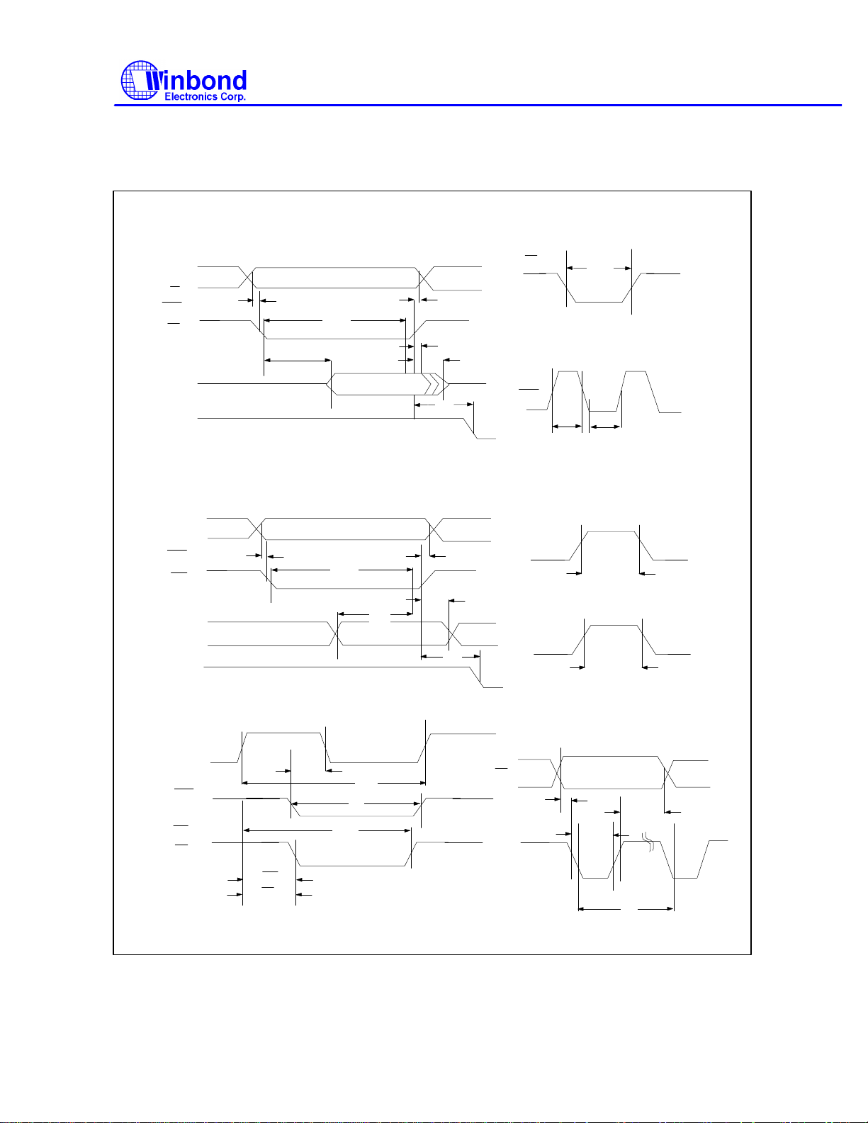
9.0 TIMING WAVEFORMS
9.1 FDC
W83787IF
SA0-SA9
AEN
CS
DACK
IOR
D0-D7
IRQ
SA0-SA9
AEN
DACK
IOW
D0-D7
IRQ
TAR
TAW
Processor Read Operation
TRR
TFD
Processor Write Operation
TWW
TDW
TDH
TR
TRA
TWI
TWA
TDF
TWD
WD
INDEX
Write Date
TWDD
Index
TIDX TIDX
Terminal Count
TC
TTC
Reset
RESET
TRST
DRQ
DACK
IOW or
IOR
TAM
TMA
TMW(IOW)
TMR(IOR)
DMA Operation
TMCY
TAA
TMRW
Drive Seek operation
DIR
TDST
TSTP
STEP
TSTD
TSC
Publication ReleaseDate:Sep 1995
- 95 - Revision A1
Page 96

9.2 IDE
W83787IF
SA<0:9>
IOR
IOW
DATA READ
IDED7
T4
D7
DATA WRITE
IDED7
D7
CS0
CS1
IOCS16
DBENL
DBENH
9.3 UART/Parallel
SIN
(RECEIVER
INPUT DATA)
IRQ3 or IRQ4
IOR
(READ RECEIVER
BUFFER REGISTER)
SERIAL OUT
(SOUT)
IRQ3 or IRQ4
IOW
(WRITE THR)
THRS
THR
T3
T1
T2
Receiver Timing
STAR
DATA BITS (5-8) PARITY
>
STOP
TSINT
<
TRINT
<>
STAR
<>
<
>
TSI
>
Transmitter Timing
<
THR
PARITYDATA (5-8)
STOP
(1-2)
STAR
>
TSTI
<
<>
IOR
(READ TIR)
TIR
<
>
Publication ReleaseDate:Sep 1995
- 96 - Revision A1
Page 97
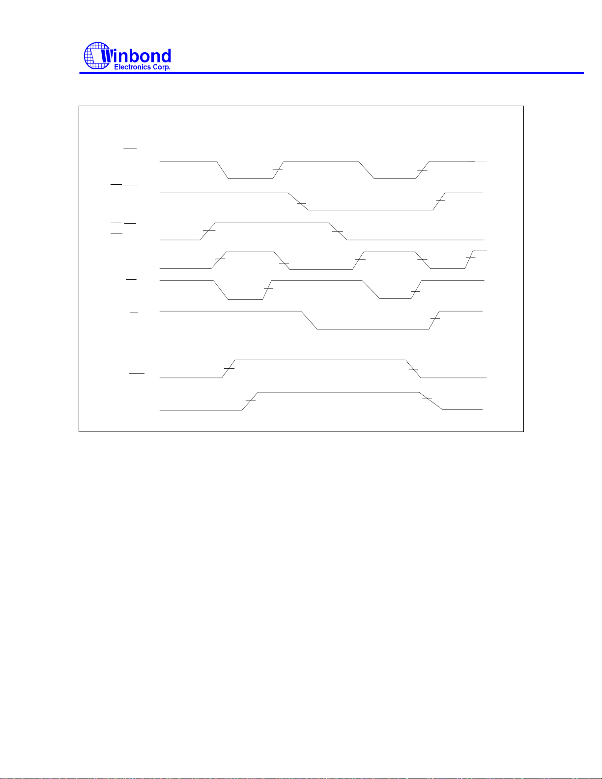
9.3.1 Modem Control Timing
W83787IF
MODEM Control Timing
IOW
(WRITE MCR)
RTS,DTR
CTS,DSR
DCD
IRQ3 or
IRQ4
IOR
(READ MSR)
RI
ACK
IRQ7
¡÷
¢x
¢x
¢x
¢x
¢
¢
¡÷
¡ö
¢x
¢x
¢x
¢
¢x
¢x
¢x
¢x
¢x
¢x
TSIM
¢
¢x
¢x
¢x
¢x
¢
¡÷
¡ö
¢x
¢x
¢x
¢x
¢
TMWO
¡÷
¢x
¢x
¢x
¢
TRIM
¡ö
¡÷
¢x
¢x
¢x
¢x
Printer Interrupt Timing
¢x
¡ö
¢x
¢x
¢
¢x
¢x
¢
¢x
¢x
¢x
¢x
¢x
¢x
¢x
¢
¡ö
¢x
¢x
¢x
¢
TSIM
¡÷
¡÷
¢x
¢x
¢x
¢x
¡ö
¢x
¢x
¢x
¢
¢x¢x¢x
¢x
¢x
¢x
¢
¢x
¢x
¢x
¢x
¢x
¢x
¢x
¢
¢
¢x
¢x
¢x
¢x
TRIM
¡ö
¢x
¢x
¢x
¢x
¢x
¢x
¢
¡ö
¢
¡ö¡÷
¢
TSIM
TLIDTLAD
TMWO
¢x
¢x
¢x
¢x
¢x
¢x
¡÷
¢x
¢
¢
Publication ReleaseDate:Sep 1995
- 97 - Revision A1
Page 98

9.4 Parallel Port
9.4.1 Parallel Port Timing
IOW
INIT,STROBE
AUTOFD, SLCTIN
PD<0:7>
ACK
IRQ (SPP)
W83787IF
t1
t2
IRQ
(EPP or ECP)
nFAULT
(ECP)
ERROR
(ECP)
IRQ
t3 t4
t5
t2
t4
Publication ReleaseDate:Sep 1995
- 98 - Revision A1
Page 99
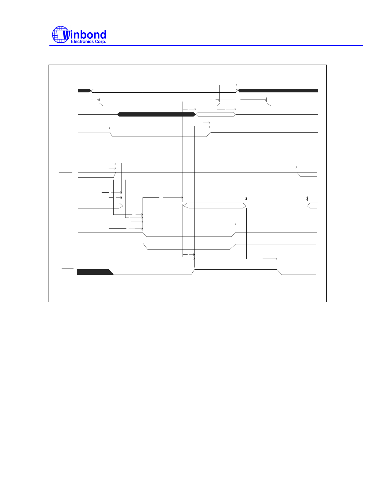
9.4.2 EPP Data or Address Read Cycle (EPP Version 1.9)
A<0:10>
IOR
SD<0:7>
IOCHRDY
t1
t6
t8
t5
t10
t9
W83787IF
t3
t2 t4
t7
WRITE
PD<0:7>
ADDRSTB
DATASTB
WAIT
t13
t14
t16
t22
t23
t24
t17
t21
t26
t18
t27
t25
t19
t15
t20
t28
Publication ReleaseDate:Sep 1995
- 99 - Revision A1
Page 100
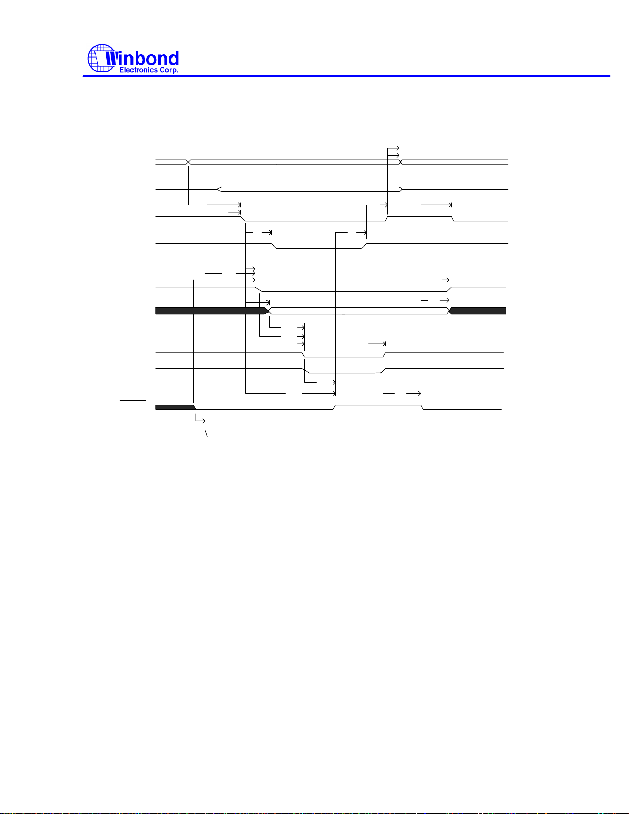
9.4.3 EPP Data or Address Write Cycle (EPP Version 1.9)
A10-A0
SD<0:7>
W83787IF
t3
t4
IOW
IOCHRDY
WRITE
PD<0:7>
DATAST
ADDRSTB
WAIT
PBDIR
t1
t22
t2
t7
t9
t10
t11
t13
t15
t16
t17
t19
t20
t5
t8
t18
t6
t12
t14
t21
Publication ReleaseDate:Sep 1995
- 100 - Revision A1
 Loading...