

Page 1
W83759A
ADVANCED VL-IDE DISK CONTROLLER
GENERAL DESCRIPTION
The W83759A is an advanced version of Winbond's popular VL-IDE interface chip, the W83759. The
W83759A retains all of the features and compatibility of the W83759 (the chip meets the ANSI ATA
4.0 specification for IDE hard disk operation and the VESA VL-Bus 2.0 specification for PC local bus
devices) while incorporating new features to meet Enhanced IDE, SFF-8011, ATA-2, and Fast-ATA
specifications.
Supports Disk Capacity of Greater than 528 MB
The W83759A's driver can handle remapping from BIOS CHS mode to HDD LBA mode. This scheme
enables users to break the 528 MB per drive barrier, allowing full use of BIOS INT13 CHS information
in drives with a capacity of up to 8.4 GB.
High Speed Host Transfer Rate
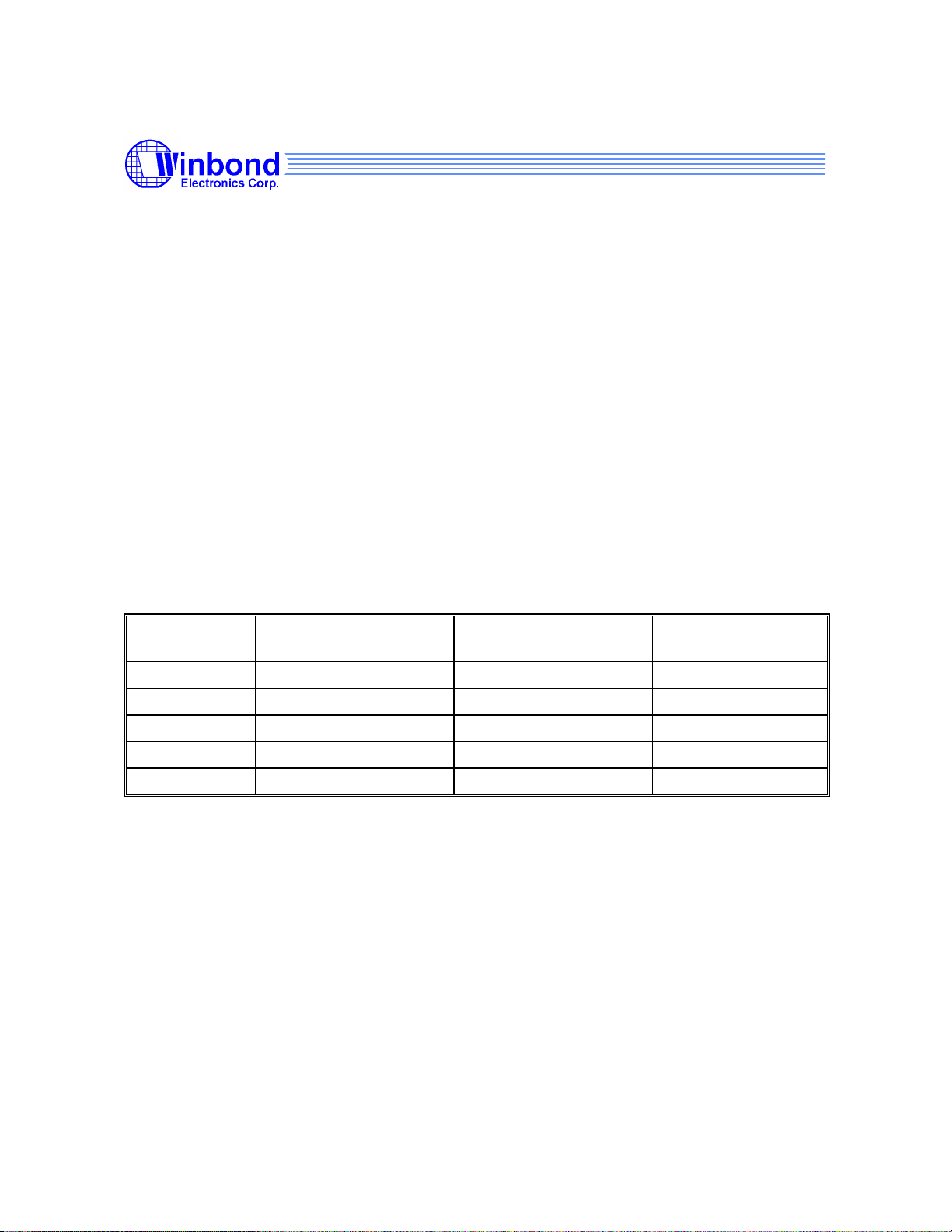
The W83759A supports Enhanced IDE PIO mode 3 and Fast ATA PIO mode 3 and 4 timing; jumper
settings or driver programming can be used to select the PIO mode and a 33 or 50 MHz VL-Bus
clock. Different programming timing can be selected for different drives in the same system. The
burst transfer rate is shown in the following table.
ATA PIO
MODE
0 600 3.33 Option
1 383 5.22 Option
2 240 8.33 Option
3 180 11.1 Required
4 120 16.6 Required
IDE COMMAND CYCLE
TIME (nS)
BURST TRANSFER
RATE (MB/sec)
IORDY THROTTLE
CONTROL
Dual IDE Channels
Like the W83759, the W83759A supports a secondary IDE address (170h-177h/376h) and IRQ15 for
applications with four hard disk drives. Additionally, the primary and secondary channels can be
independently enabled or disabled by jumper settings or software programming.
Non-disk IDE Peripherals
Because the command cycle can be programmed individually for each drive and dual IDE channels
are supported, non-disk IDE peripherals (such as an ATAPI CD-ROM or tape drive) can be attached
to the secondary IDE without affecting the transfer rate of the ATA disk drive. Sales of ATAPI IDE
CD-ROMs are expected to grow rapidly as these devices become a standard part of many users'
desktop PC setup.
Publication Release Date: May 1995
- 1 - Revision A1
Page 2
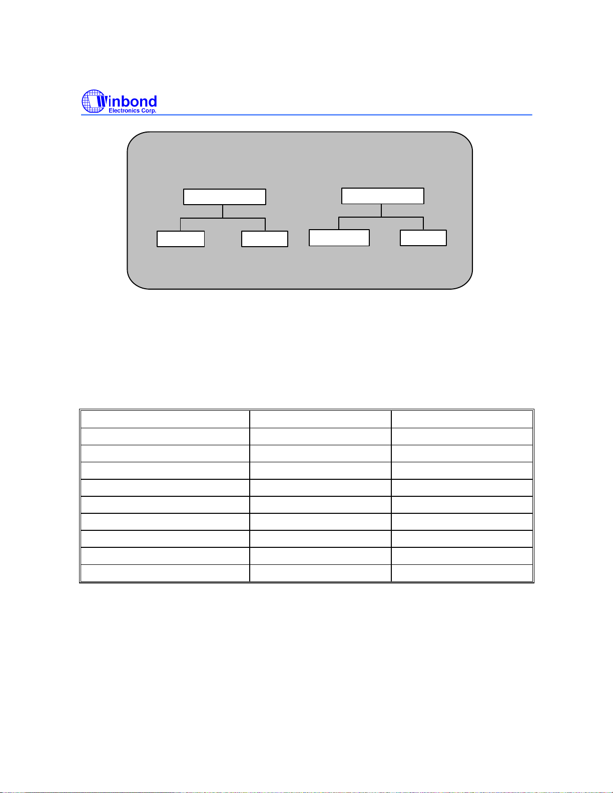
Enhanced IDE/Fast ATA Dual Channel Structure
W83759A
Primary Channel
40-pins
Disk
< 8.4 GB
PD0
The W83759A provides all of the next-generation ATA-IDE requirements, including support for high
capacity disk drives, high speed host transfers, multiple IDE peripherals, and non-disk IDE
peripherals. It makes high-performance, low-cost, easy-to-use IDE machines possible.
The W83759A is pin-to-pin backward compatible with the W83759. In addition to the advanced
features described above, the W83759A supports automatic power-down, standby, and suspend APM
power management states for green PC applications. This new chip is packaged in a 100-pin QFP.
The table below compares the W83759 and W83759A:
Dual Channel IDE Yes Yes
8.4 G Max. Cap. Software Driving Software Driving
Disk
< 8.4 GB
PD1
W83759 W83759A
Secondary Channel
40-pins
CD ROM
ATAPI ATAPI
SD0
SD1
Tape
PIO Mode 3, 4 Control No Yes*
DMA Mode Control No Yes*
IOCHRDY Control No Yes*
IDE Timing Control Jumper Jumper or Driver*
Prefetch Control No Yes*
Power Saving Control No Yes*
ATAPI Protocol Software Driving Software Driving
* All control is drive-by-drive (per drive selectability)
- 2 -
Page 3

W83759A
FEATURES
• Pin-to-pin backward compatible with W83759 VL-IDE Interface chip
• VESA VL-Bus Rev 2.0 compatible, connects directly to local bus and four IDE drives
• Direct interface to various ANSI ATA/ATA-2/FAST ATA/IDE-2/Enhanced IDE drives
• Supports 32 and 16-bit data transfer
• Fully software programmable for command active/recovery time and address setup, data hold
time
• Built-in VL-Bus to 16-bit IO data buffer for special applications
• Fully supports Enhanced IDE features, including Fast PIO, Mode 3/4, IORDY flow control,
prefetch control
• Supports dual channels to allow up to four drives or non-disk devices (ATAPI CD-ROM and tape
drives)
• Pipeline pre-fetched reads and posted writes for concurrent disk and host operations
• Independent access timing for all drives (primary/secondary and master/slave)
• All Enhanced IDE new features may be disabled/enabled via driver or power-on setting by per
drive selectability
• ATA/Mode 0-4 PIO speed may be set as default timing of each drive via power-on jumper setting
• Supports slave DMA mode protocol (reserved)
• Supports auto power-down, standby, suspend APM power management state for green PCs
• Primary and secondary channel can be independently enabled/disabled by software or jumper
setting
• Supports drivers for DOS, Windows, OS/2, UNIX, and Netware
• Packaged in 100-pin QFP
Publication Release Date: May 1995
- 3 - Revision A1
Page 4
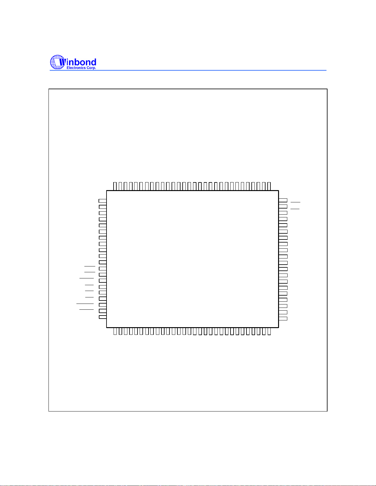
PIN CONFIGURATION
I
I
D
D
D
D
7
8
Sa
Sa
m
mp
pl
le
e
Te
Te
xt
xt
80 79 78 77 76 75 74 73 72 71 70 69 68 67 66 65 64 63 62 61 60 59 58 57 56 55 54 53 52 51
X
IDD6
IDD5
IDD4
IDD3
IDD2
IDD1
IDD0
GND
LCLK
GND
Vcc
LDEV
LRDY
RDYRTN
LADS
HWR
HMIO
IORDY/HDC
SYSRST
ADV
81
X
82
X
83
X
84
X
85
X
86
X
87
X
88
X
89
X
90
X
91
X
92
X
93
X
94
X
95
X
96
X
97
X
98
X
99
X
100
1 2 3 4 5
Sa
Sa
m
mp
pl
le
e
Te
Te
xt
xt
W83759A
/
I
E
S
T
N
E
I
S
D
T
I
I
I
D
D
D
/
E
E
/
I
I
I
I
D
D
D
D
D
D
D
D
1
1
1
9
1
2
0
Sa
Sa
Sa
Sa
mp
mpl
mpl
mp
le
e
e
le
Te
Tex
Tex
Te
t
t
xt
xt
6 7 8 9
Sa
Sa
Sa
Sa
mpl
mpl
mp
mp
e
e
le
le
Te
Tex
Tex
Te
xt
t
t
xt
I
I
I
I
D
D
D
D
E
D
D
D
I
1
1
1
O
3
4
5
W
Sa
Sa
Sa
mpl
mpl
mpl
e
e
e
Tex
Tex
Tex
t
t
t
10 11 12 13 14 15 16
Sa
Sa
Sa
mpl
mpl
mpl
e
e
e
Tex
Tex
Tex
t
t
t
Sa
mp
le
Te
xt
Sa
mp
le
Te
xt
E
I
A
A
A
D
2
1
0
E
,
,
,
M
S
I
M
D
P
O
D
0
1
R
1
Sa
Sa
Sa
Sa
mpl
mp
mpl
mp
e
le
e
le
Tex
Te
Tex
Te
t
xt
t
xt
Sa
Sa
Sa
Sa
mpl
mp
mpl
mp
e
le
e
le
Tex
Te
Tex
Te
t
xt
t
xt
E
,
,
/
/
I
I
D
D
E
E
1
1
G
V
C
C
N
c
S
S
D
c
1
0
Sa
mp
le
Te
xt
17 18 19 20 21 22 23 24 25 26 27 28 29 30
Sa
mp
le
Te
xt
/
D
D
E
A
N
C
H
K
/
,
,
/
I
/
/
I
D
V
V
D
E
E
G
G
0
0
A
A
O
O
C
C
S
E
E
S
S
D
L
H
1
0
7
XXXXX
XXXXX XXXXX XXXXX
S
S
S
D
D
5
6
XXXXX XXXXX
S
S
S
S
D
D
D
D
D
2
1
4
3
0
X
50
49
48
47
46
45
44
43
42
41
40
39
38
37
36
35
34
33
32
31
AEN
X
XIOW
X
XIOR
X
SA1
X
SA0
X
HD0
X
HD1
X
HD2
X
HD3
X
Vcc
X
GND
X
HD4
X
HD5
X
HD6
X
HD7
X
HD8
X
HD9
X
HD10
X
HD11
X
HD12
/
/
H
B
B
A
E
E
2
2
0
H
H
H
H
H
G
H
H
H
H
H
H
H
H
H
H
H
H
H
H
H
H
H
A
A
A
A
3
4
5
A
A
A
6
9
7
8
H
D
D
D
D
3
3
2
2
1
0
9
8
H
N
D
D
D
D
D
D
D
2
2
2
7
6
5
D
2
2
2
2
4
3
2
1
H
D
D
D
D
2
1
1
1
0
9
8
7
H
D
D
D
D
1
1
1
1
6
5
4
3
- 4 -
Page 5
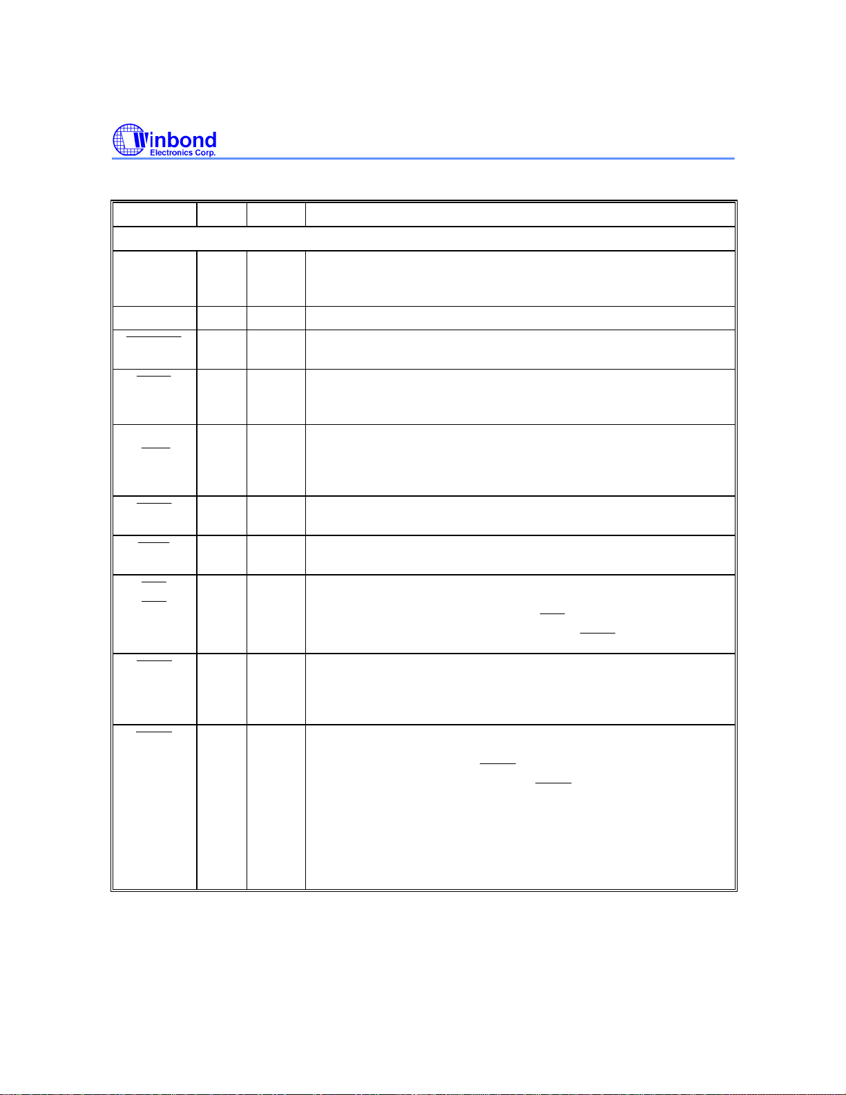
PIN DESCRIPTION
SYSRST
LADS
HDC
HMIO
HWR
BE2
BE0
BE2
LDEV
LDEV
LRDY
LRDY
LRDY
SYMBOL PIN TYPE DESCRIPTION
VL-Bus Interface
ADV 100 I-PU Advanced mode indicator.
When high, chip is in W83759A mode. When low, chip is in
W83759 mode.
LCLK 89 I VL-Bus clock.
99 I System reset.
When active, the power-on setting pin acts as input.
95 I Address data strobe.
An active low input signal indicates that there is a valid address
and command on the bus.
W83759A
IORDY
/
98 I In W83759A mode: Enhanced IDE IORDY flow control input. Used
to throttle disk's PIO data transfers to improve PIO mode.
In W83759 mode: Host data or code status. Used to distinguish
between IO and interrupt or halt cycles.
97 I-PU Host memory or I/O status.
Used to distinguish between memory and I/O cycles.
96 I Host write or read status.
Used to distinguish between write and read cycles.
1
2
92 O Local device.
93 Tri-O Local ready.
I Byte enable bits 2 and 0 from the host CPU address bus.
These active low inputs specify which bytes will be valid for host
read and write data transfers. When
a 32-bit hard disk data transfer cycle when
An active low output signal which indicates that the current host
CPU command cycle is a valid W83759A I/O address (1F0h or
170h).
An active low output that indicates when a CPU transfer has been
completed. During a cycle
high. When the cycle is completed,
pulled low and will remain active for one T-state. Then it will drive
high for one T-state before finally being disabled to end the
sequence.
This signal is shared with all other VL-Bus targets and driven by
W83759A only during cycles W83759A has claimed as its own.
will first be enabled and driven
is low, the host performs
is active.
will immediately be
Publication Release Date: May 1995
- 5 - Revision A1
Page 6
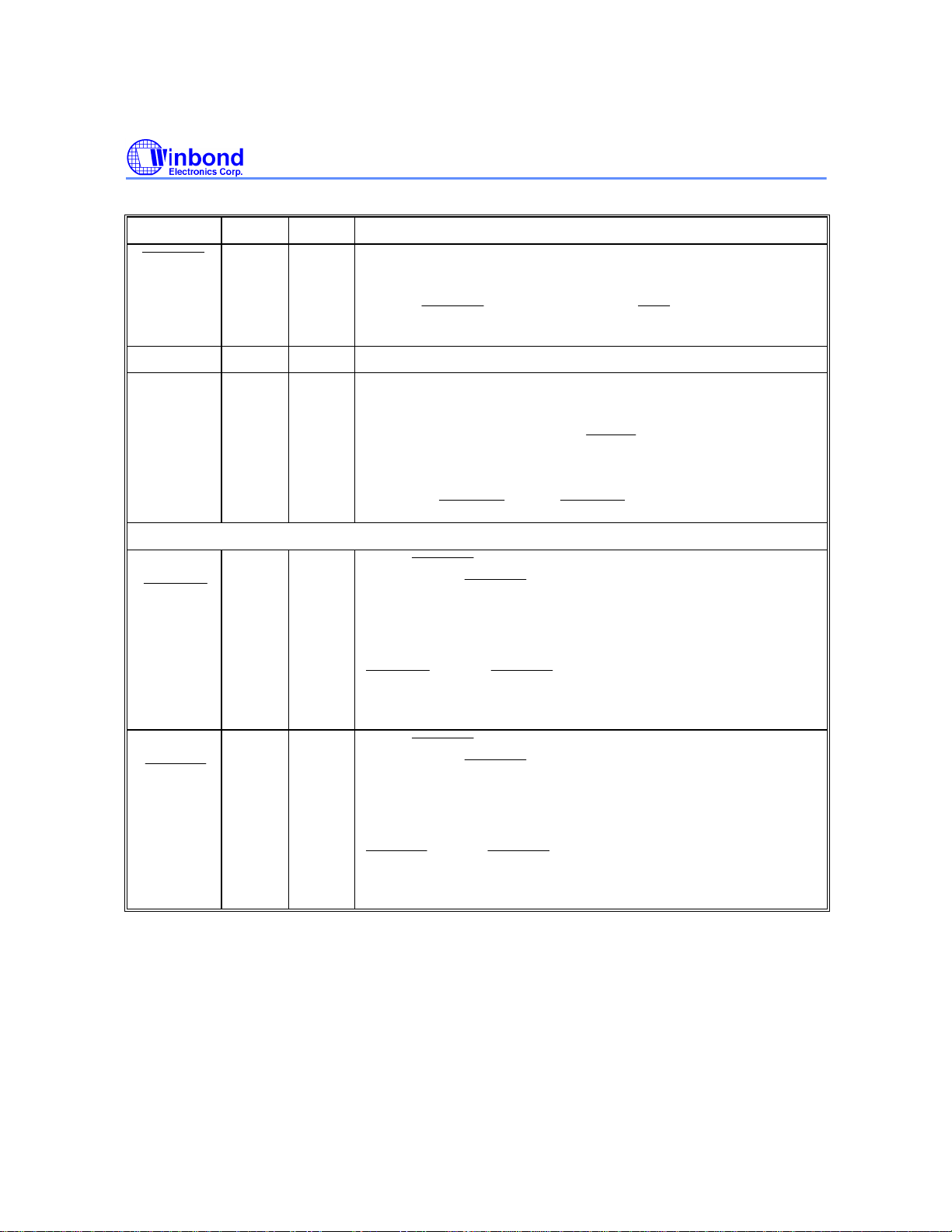
Pin Description, continued
RDYRTN
RDYRTN
RDY
[
]
VGAOEH
VGAOEL
IDE0CS0
SYSRST
SYSRST
IDE0CS0
SYSRST
IDE0CS1
SYSRST
SYSRST
IDE0CS1
SYSRST
SYMBOL PIN TYPE DESCRIPTION
94 I Ready return.
An active low signal that indicates the end of the current host
CPU transfer.
Usually
CPU.
HA[9:2] 10-3 I Host address bits 9 through 2 from the host address bus.
is tied directly to the
signal of the host
W83759A
HD[31:0]
PRDYEN
/
SRDYEN
/
11−14
19−39
42−45
61 I/O
62 I/O
I/O Host data.
This is the 32-bit bidirectional data bus that connects to the host
CPU. HD[7:0] define the lowest data byte, while D[31:24] define
the most significant byte by the
normally in a high-impedance state and is driven by the
W83759A only during data register (1F0h or 170h) read cycles
and VGA (
When
-PU
-PU
rising edge of
PRDYEN: A high input enables the IORDY flow control function of
the primary channel (IDE0) and a low input disables the IDE0's
flow control function.
output used to select the command block registers in the IDE0
drive (1F0h−1F7h).
When
rising edge of
SRDYEN: A high input enables the IORDY flow control function of
the secondary channel (IDE1) and a low disables the IDE1's flow
control function.
= 0 or
Drive Interface
is active, this is an input that latches on the
: When
is active, this is an input that latches on the
BE 2:0 signals. The HD bus is
= 0) read cycles.
.
is inactive, this pin is an active low
.
: When
output used to select the alternate status register of the control
block registers in the IDE0 drive (3F6).
- 6 -
is inactive, this pin is an active low
Page 7
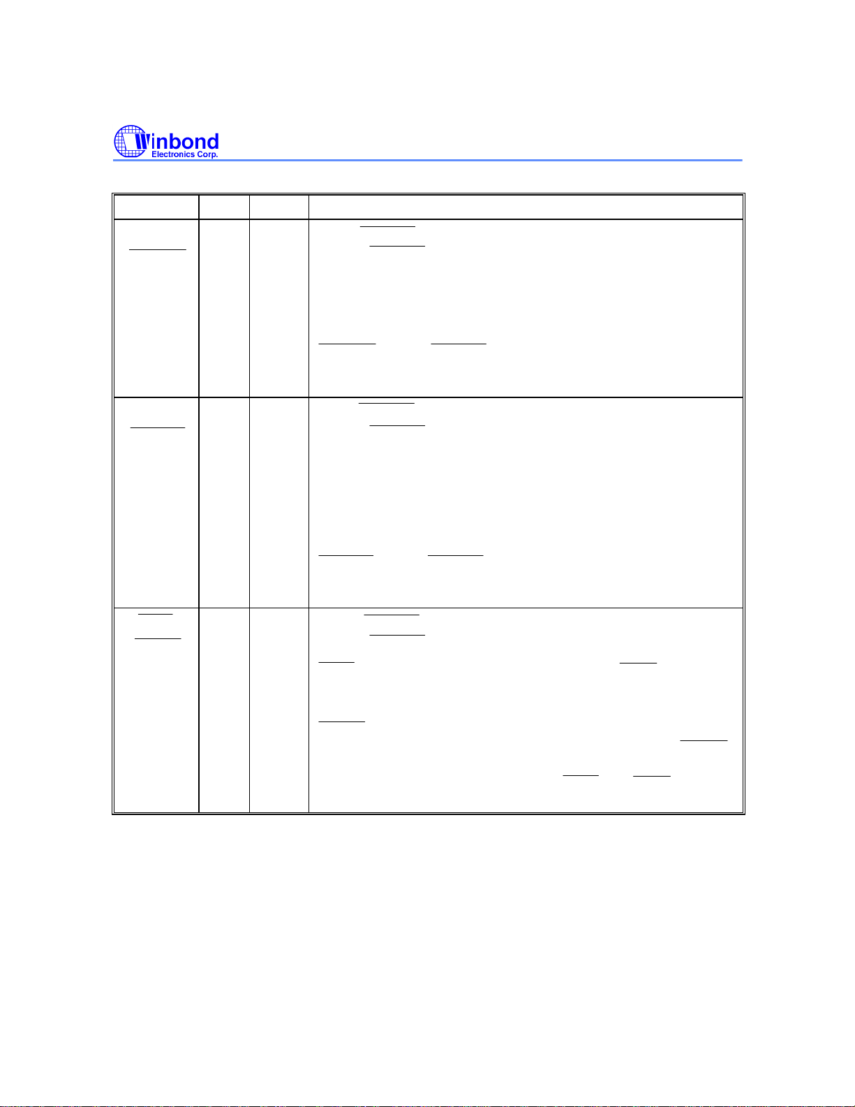
Pin Description, continued
IDE1CS0
SYSRST
SYSRST
IDE1CS0
SYSRST
IDE1CS1
SYSRST
SYSRST
IDE1CS1
SYSRST
EMD
1
IDEIOR
SYSRST
SYSRST
EMD1
EMD
0
IDEIOR
IDEIOR
EMD1
EMD
0
SYMBOL PIN TYPE DESCRIPTION
W83759A
ENIDE
/
TEST
/
/
63 I/O
-PU
64 I/O
-PU
70 I/O
-PU
When
edge of
ENIDE: In W83759 mode (ADV = low), this power-on-setting pin
controls if the chip enable or disable. In W83759A mode (ADV =
high), this pin controls if the IDE0 channel enable or disable. A high
input enables and a low input disables the IDE0 channel.
output and is used to select the command block registers in the
IDE1 drive (170h−177h).
When
edge of
TEST: In W83759 mode, this power-on-setting pin controls whether
both dual channels are enabled or only the primary channel is
enabled. A high input enables IDE0 and IDE1 simultaneously and a
low input enables IDE0 only. In W83759A mode, this pin controls
whether the IDE1 channel enable or disable controls the IDE0
channel as ENIDE.
output used to select the alternate status register of the control
block registers in the IDE1 drive (376).
When
edge of
is active, this is an input that latches on the rising
.
: When
is active, this is an input that latches on the rising
.
: When
is active, this is an input that latches on the rising
.
is inactive, this pin is an active low
is inactive, this pin is an active low
: This power-on-setting pin combines with
initial enhanced timing mode of hard disk access cycles when the
enhanced mode is selected via the POSS3 configuration register.
: Drive I/O read. An active low output that enables data to
be read from the drive. The duration and repetition rate of
cycles are determined by the type of IDE drive, as specified by
MD1 and MD0, in W83759 mode or by
W83759A enhanced mode.
Publication Release Date: May 1995
- 7 - Revision A1
and
to set the
in
Page 8
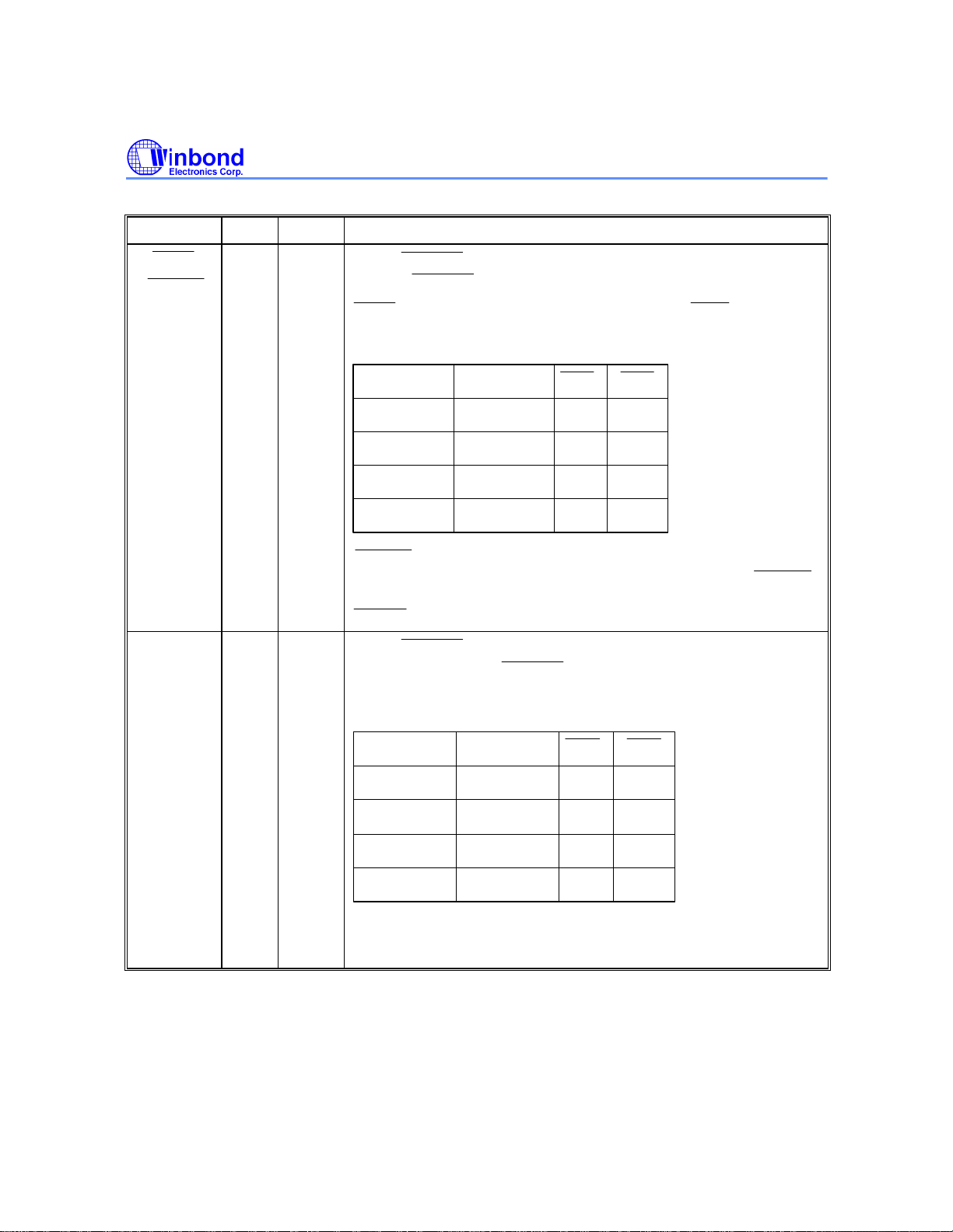
Pin Description, continued
EMD
0
IDEIOW
SYSRST
SYSRST
EMD
0
EMD
1
IDEIOW
IDEIOW
IDEIOR
SYSRST
SYSRST
SYMBOL PIN TYPE DESCRIPTION
W83759A
/
MD1
/IDEA2,
MD0
/IDEA1
71 I/O
-PU
69
I/O
-PD
68
When
edge of
: This power-on-setting pin combines with
is active, this is an input that latches on the rising
.
to set the
initial enhanced timing mode of hard disk access cycles when the
enhanced mode is selected via the POSS3 configuration register.
ATA PIO mode
2
3
3
4
Access Time
240 nS
180 nS
180 nS
120 nS
EMD1
1
1
0
0
EMD0
1
0
1
0
: Drive I/O write. An active low output that enables data to
be written to the drive. The duration and repetition rate of
cycles are determined by the type of IDE drive, as specified by
.
When
on the rising edge of
is active, these pins function as inputs and latch
.
MD1, MD0: ATA mode of IDE Drive. MD0 and MD1 are used to
select the hard disk access time.
ATA PIO mode
0
0+
1
2
Access Time
600 nS
500 nS
400 nS
240 nS
EMD1
0
0
1
1
EMD0
0
1
0
1
IDEA2, IDEA1: IDE drive address bits 2 and 1. Drive address bits 2
and 1 are outputs to the IDE connector for register selection in the
drive.
- 8 -
Page 9
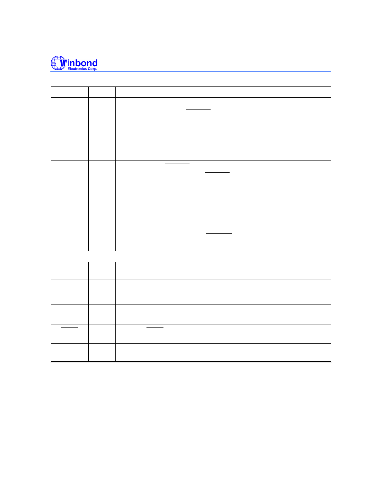
Pin Description, continued
SYSRST
SYSRST
SYSRST
SYSRST
VGAOEH
VGAOEL
XIOR
XIOR
XIOW
XIOW
SYMBOL PIN TYPE DESCRIPTION
W83759A
SP1
/IDEA0
IDD[15:0]
SA[1:0] 47, 46 I ISA address bits 1 and 0.
67 I/O
72−87
-PD
I/O
-PU
When
rising edge of
SP1: VL-Bus speed select. A high input configures the W83759A
to run at from 33 MHz to 50 MHz; a low input configures the
W83759A to run at under 33 MHz.
IDEA0: IDE drive address bit 0. Drive address bit 0 is output to
the IDE connector for register selection in the drive.
When
on the rising edge of
As power-on setting pins, IDD[15:8] are latched to the POSS3
register and IDD[7:0] are latched to the POSS2 register.
As the drive data bus, bits 15 through 0 are the 16-bit bidirectional
data bus that connects to the IDE drive.
IDD[7:0] define the lowest data byte. The IDD bus is normally in a
pull-high state and is driven with valid data by the W83759A only
during IDE or VGA (
ISA-Bus Interface
Used to select the hard disk I/O registers.
is active, this pin is an input that latches on the
is active, these pins function as inputs and latch
= 0) write cycles.
.
.
= 0 or
SD[7:0] 58-51 I/O These signals provide data bus bits 0 through 7 for the CPU and
IDE I/O devices. SD0 is the least significant bit and SD7 is the
most significant bit.
48 I
49 I
AEN 50 I When this line is active (high), the DMA controller has control of
instructs the hard disk I/O device to drive its data onto the
SD data bus.
instructs the hard disk I/O device to read the data on the
SD data bus.
the address bus. A low is the address enable.
Publication Release Date: May 1995
- 9 - Revision A1
Page 10
Pin Description, continued
SUSP
DACK
VGAOEH
SUSP
DACK
VGAOEH
DMASL
VGAOEL
ISDENH
SYSRST
SYSRST
DMASL
VGAOEL
ISDENH
SYMBOL PIN TYPE DESCRIPTION
Special Bus Control Interface
W83759A
,
,
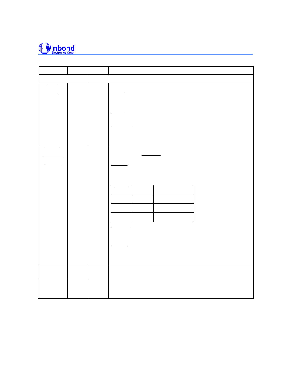
59 I-PU This pin is a multi-function input pin.
: In suspend enable mode, indicates that the W83759A
will enter the suspend state when low and resume operation when
high.
: In DMA transfer enable mode, used to indicate when the
DMA transfer cycle occurs.
: In VGA buffer enable mode, this active low input
controls the input enable for the data transceivers that connect
the ID[15:0] pins to the HD[31:16] pins.
,
/
60 I/O
-PU
When
rising edge of
: This power-on setting pin combines with SUSPEN
is active, this pin is an input that latches on the
.
(IDD11 power-on setting pin) to determine which mode the
W83759A is in.
DMASL
1
0
0
SUSPEN
X
1
0
Mode
VGA buffer enable
Suspend enable
DMA transfer enable
Vcc 41, 65,
91
GND 15, 40,
66, 88,
90
: In VGA buffer enable mode, this active low input
controls the input enable for the data transceivers that connect
the ID[15:0] pins to the HD[15:0] pins.
: In DMA transfer enable mode, this output pin controls
the activity of the high byte buffer between IDD[15:8] and
SD[15:8].
+5V power supply
Ground reference
- 10 -
Page 11
W83759A
CONFIGURATION REGISTERS
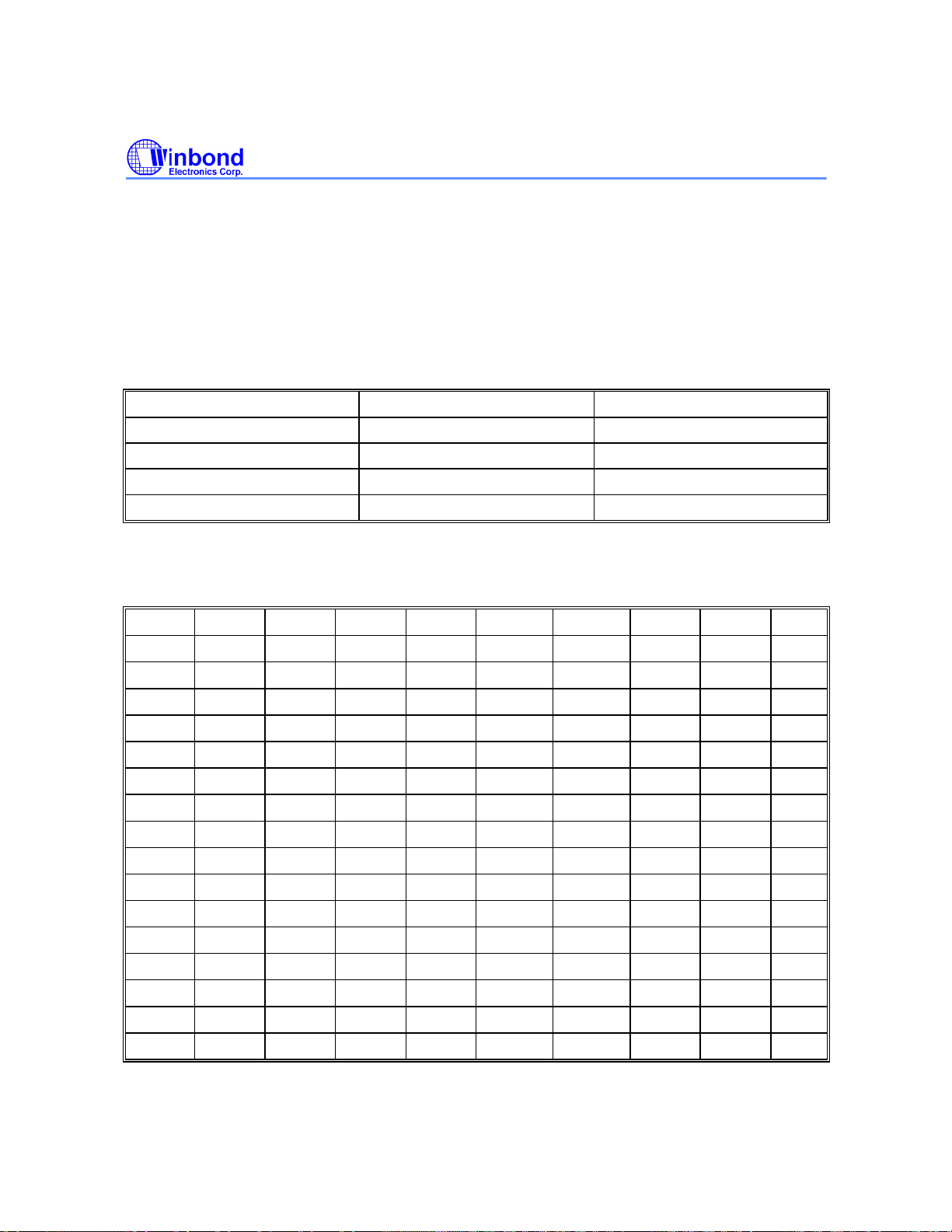
Several configuration registers are implemented in the W83759A. These registers are accessible in
single-chip mode through the index/data port. The index/data port address is 1B4h/1B8h or
134h/138h, depending on whether pin IDD0 is high or low at power-on.
When the W83759A is in multi-chip mode (IDD1 is low at power-on setting), an ID code should be
written to 1B0h/130h (IDIN port). The W83759A will then enter the programming sequence if the ID
code matches the chip ID (determined by IDD2, IDD3 at power-on setting) or leave the programming
sequence if the ID code does not match. After the chip has entered the programming sequence, the
chip ID can be read by reading 1BCh/13Ch (IDOUT port).
IDD0_P is HIGH IDD0_P is LOW
IDIN port (W/O) 1B0h* 130h**
Index port (R/W) 1B4h 134h
data port (R/W) 1B8h 138h
IDOUT port (R/O) 1BCh 13Ch
* The alias base addresses of 1B0h are XB0h and YB0h, where "X" means 0, 4, 8, C and "Y" means 1, 5, 9, D.
** The alias base addresses of 130h are X30h and Y30h, where "X" means 0, 4, 8, C and "Y" means 1, 5, 9, D.
Index map of configuration registers:
INDEX Bit 7 Bit 6 Bit 5 Bit 4 Bit 3 Bit 2 Bit 1 Bit 0 Default
80h(R/O)
POSS1
81h(R/W)
POSP1
82h(R/O)
POSS2
83h(R/W)
POSP2
84h(R/O)
POSS3
85h(R/W)
POSP3
86h(R/W)
ALTCTL
87h(R/O)
REVID
88h(R/W)
PD0TIM0
89h(R/W)
PD0TIM1
8Ah(R/W)
PD1TIM0
8Bh(R/W)
PD1TIM1
8Ch(R/W)
SD0TIM0
8Dh(R/W)
SD0TIM1
8Eh(R/W)
SD1TIM0
8Fh(R/W)
SD1TIM1
ADV SP1 MD1 MD0 PRDYEN SRDYEN IDEN1 IDEN0 8Fh
ADV_P SP1_P MD1_P MD0_P PRDYEN_P SRDYEN_P IDEN1_P IDEN0_P 8Fh
PD0LEN PD1LEN SD0LEN SD1LEN DSL1 DSL0 CRLK# CRSL FFh
PD0LE_P PD1LEN_P SD0LEN_P SD1LEN_P DSL1_P DSL0_P CRLK#_P CRSL_P FFh
PD0EM# PD1EM# SD0EM# SD1EM# SUSPEN STBY# APD SWAP# FFh
PD0EM#_P PD1EM#_P SD0EM#_P SD1EM#_P SUSPEN_P STBY#_P APD_P SWAP#_P FFh
DMASL#_PReserved EMD1 EMD0 PEMD1_P PEMD0_P SEMD1_P SEMD0_P 80h
DMASL# Reserved PDRV SDRV Rev 3 Rev 2 Rev 1 Rev 0 8Ah
PD0ACT3 PD0ACT2 PD0ACT1 PD0ACT0 PD0RCV3 PD0RCV2 PD0RCV1 PD0RCV0 00h
PD0AST1 PD0AST0 PD0DHT1 PD0DHT0 PD0PRE# PD0DMA# PD0RDY# PD0ADV 00h
PD1ACT3 PD1ACT2 PD1ACT1 PD1ACT0 PD1RCV3 PD1RCV2 PD1RCV1 PD1RCV0 00h
PD1AST1 PD1AST0 PD1DHT1 PD1DHT0 PD1PRE# PD1DMA# PD1RDY# PD1ADV 00h
SD0ACT3 SD0ACT2 SD0ACT1 SD0ACT0 SD0RCV3 SD0RCV2 SD0RCV1 SD0RCV0 00h
SD0AST1 SD0AST0 SD0DHT1 SD0DHT0 SD0PRE# SD0DMA# SD0RDY# SD0ADV 00h
SD1ACT3 SD1ACT2 SD1ACT1 SD1ACT0 SD1RCV3 SD1RCV2 SD1RCV1 SD1RCV0 00h
SD1AST1 SD1AST0 SD1DHT1 SD1DHT0 SD1PRE# SD1DMA# SD1RDY# SD1ADV 00h
Value
Publication Release Date: May 1995
- 11 - Revision A1
Page 12
W83759A
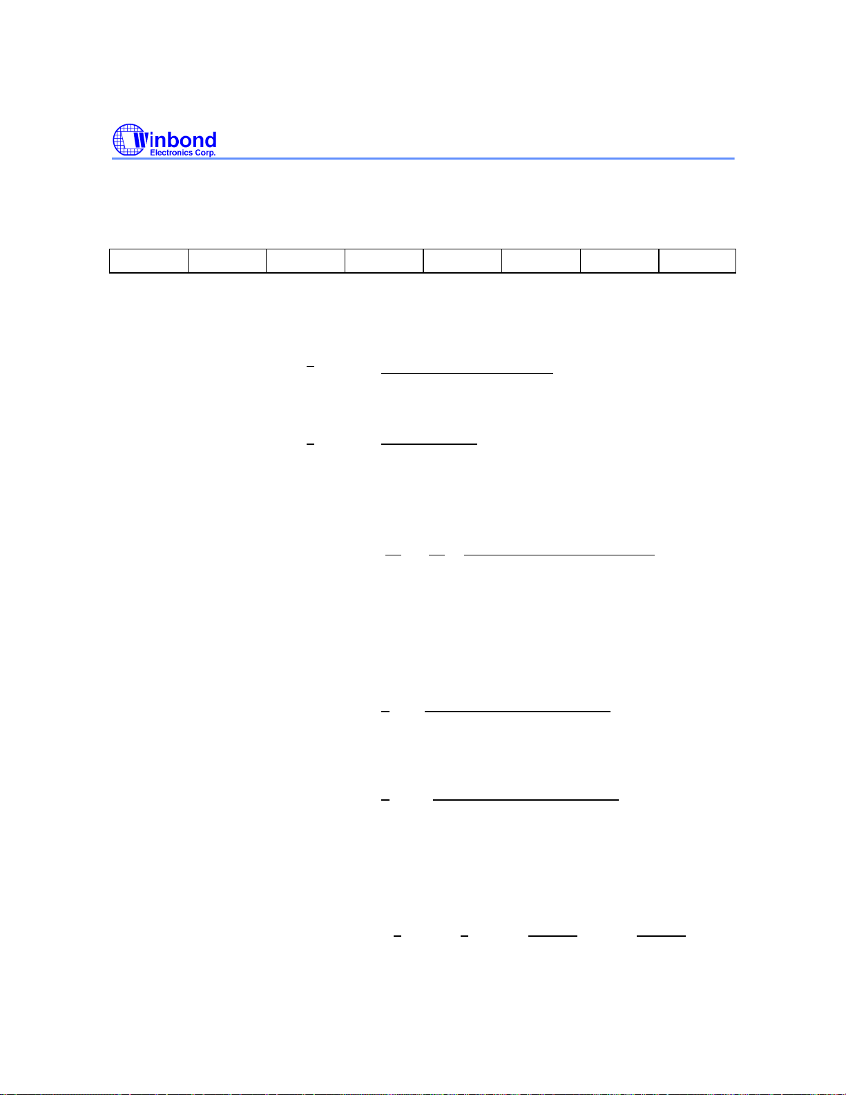
CRX80h (POSS1) Read Only Power-on Setting Status 1
Bit7 Bit6 Bit5 Bit4 Bit3 Bit2 Bit1 Bit0
ADV SP1 MD1 MD0 PRDYEN SRDYEN IDEN1 IDEN0
Bit 7 ADV Power-on setting value of ADV pin
Initial application mode
0
1
Bit 6 SP1 Power-on setting value of IDEA0 pin
0
1
Bit 5, 4 MD1, MD0 Power-on setting value of IDEA2, IDEA1 pin
Bit 3 PRDYEN Power-on setting value of IDE0CS0 pin
Bit 2 SRDYEN Power-on setting value of IDE0CS1 pin
No advanced mode application
Advanced mode application
Select VESA bus operating CLK
VLCLK 33 MHz
VLCLK > 33 MHz
Default HDD host transfer mode
MD1 MD0
0 0 Mode 0 (cycle time = 600 nS)
0 1 Mode 0+ (cycle time = 500 nS)
1 0 Mode 1 (cycle time = 400 nS)
1 1 Mode 2 (cycle time = 240 nS)
Initial state of primary channel IOCHRDY flow control
0 Disable IOCHRDY flow control
1 Enable IOCHRDY flow control
Initial state of secondary channel IOCHRDY flow control
0 Disable IOCHRDY flow control
1 Enable IOCHRDY flow control
Bit 1, 0 IDEN1, IDEN0 Power-on setting value of IDE1CS1, IDE1CS0 pins
Initial state of IDE ENable control
when ADV_P
= 0
IDEN1 IDEN0 Primary IDE Secondary IDE
X 0 disabled disabled
0 1 enabled disabled
1 1 enabled enabled
- 12 -
Page 13

W83759A
Continued
when ADV_P
= 1
CRX81h (POSP1) Read / Write Power-on Setting Programming 1
Bit 7 Bit 6 Bit 5 Bit 4 Bit 3 Bit 2 Bit 1 Bit 0
ADV_P SP1_P MD1_P MD0_P PRDYEN_P SRDYEN_P IDEN1_P IDEN0_P
After power-on, the content of the POSP1 register is equal to that of the POSS1 register. The host
can program POSP1 to modify the power-on settings.
Bit 7 ADV_P Programming application mode
IDEN1 IDEN0 Primary IDE Secondary IDE
0 0 disabled disabled
1 0 disabled enabled
0 1 enabled disabled
1 1 enabled enabled
0 No advanced mode application
1 Advanced mode application
Bit 6 SP1_P Select VESA bus operating CLK
0 VLCLK 33 MHz
1 VLCLK > 33 MHz
Bit 5, 4 MD1_P,
MD0_P
Bit 3 PRDYEN_P Primary channel IOCHRDY flow control
Bit 2 SRDYEN_P Secondary channel IOCHRDY flow control
Bit 1, 0 IDEN1_P,
IDEN0_P
Select default HDD host transfer mode
MD1_P MD0_P
0 0 Mode 0 (cycle time = 600 nS)
0 1 Mode 0+ (cycle time = 500 nS)
1 0 Mode 1 (cycle time = 400 nS)
1 1 Mode 2 (cycle time = 240 nS)
0 Disable IOCHRDY flow control
1 Enable IOCHRDY flow control
0 Disable IOCHRDY flow control
1 Enable IOCHRDY flow control
IDE ENable control
Publication Release Date: May 1995
- 13 - Revision A1
Page 14
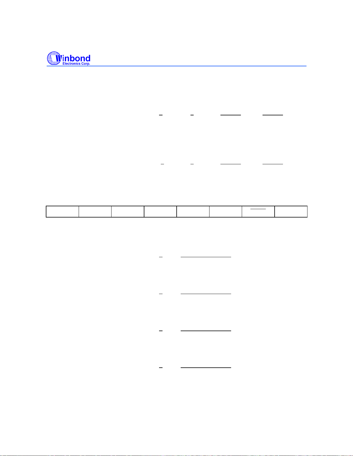
Continued
CRLK
when ADV_P
= 0
W83759A
IDEN1_P IDEN0_P Primary IDE Secondary IDE
X 0 disabled disabled
0 1 enabled disabled
1 1 enabled enabled
when ADV_P
= 1
CRX82h (POSS2) Read Only Power-on Setting Status 2
Bit 7 Bit 6 Bit 5 Bit 4 Bit 3 Bit 2 Bit 1 Bit 0
PD0LEN PD1LEN SD0LEN SD1LEN DSL1 DSL0
Bit 7 PD0LEN Power-on setting value of IDD7 pin
Bit 6 PD1LEN Power-on setting value of IDD6 pin
IDEN1_P IDEN0_P Primary IDE Secondary IDE
0 0 disabled disabled
1 0 disabled enabled
0 1 enabled disabled
1 1 enabled enabled
Initial Primary Drive 0 (PD0) local device control
0 Disable local device
1 Enable local device
Initial Primary Drive 1 (PD1) local device control
0 Disable local device
1 Enable local device
CRSL
Bit 5 SD0LEN Power-on setting value of IDD5 pin
Initial Secondary Drive 0 (SD0) local device control
0 Disable local device
1 Enable local device
Bit 4 SD1LEN Power-on setting value of IDD4 pin
Initial Secondary Drive 1 (SD1) local device control
0 Disable local device
1 Enable local device
- 14 -
Page 15

Continued
CRLK
CRLK
W83759A
Bit 3, 2 DSL1, 0 Power-on setting value of IDD3, IDD2 pin
Initial Device ID selection (used in multi-chip mode or
CR protection scheme)
DSL1 DSL0 Device ID
0 0 60h
0 1 61h
1 0 62h
1 1 63h
Bit 1
Bit 0 CRSL Power-on setting value of IDD0 pin
CRX83h (POSP2) Read / Write Power-on Setting Programming 2
Bit 7 Bit 6 Bit 5 Bit 4 Bit 3 Bit 2 Bit 1 Bit 0
PD0LEN_PPD1LEN_PSD0LEN_P SD1LEN_P DSL1_P DSL0_P
After power-on, the content of the POSP2 register is equal to that of the POSS2 register. The host
can program POSP2 to modify the power-on settings.
Bit 7 PD0LEN_P Primary Drive 0 (PD0) local device control
Power-on setting value of IDD1 pin
Initial Configuration Register locked control
0 CR is auto-locked (used in multi-chip mode)
1 CR is not auto-locked (used in single-chip mode)
Initial Configuration Register selection
0 CR port address: 130h, 134h, 138h, 13Ch
1 CR portaddress: 1B0h, 1B4h, 1B8h, 1BCh
CRSL_P
_P
0 Disable local device
1 Enable local device
Bit 6 PD1LEN_P Primary Drive 1 (PD1) local device control
0 Disable local device
1 Enable local device
Bit 5 SD0LEN_P Secondary Drive 0 (SD0) local device control
0 Disable local device
1 Enable local device
Publication Release Date: May 1995
- 15 - Revision A1
Page 16
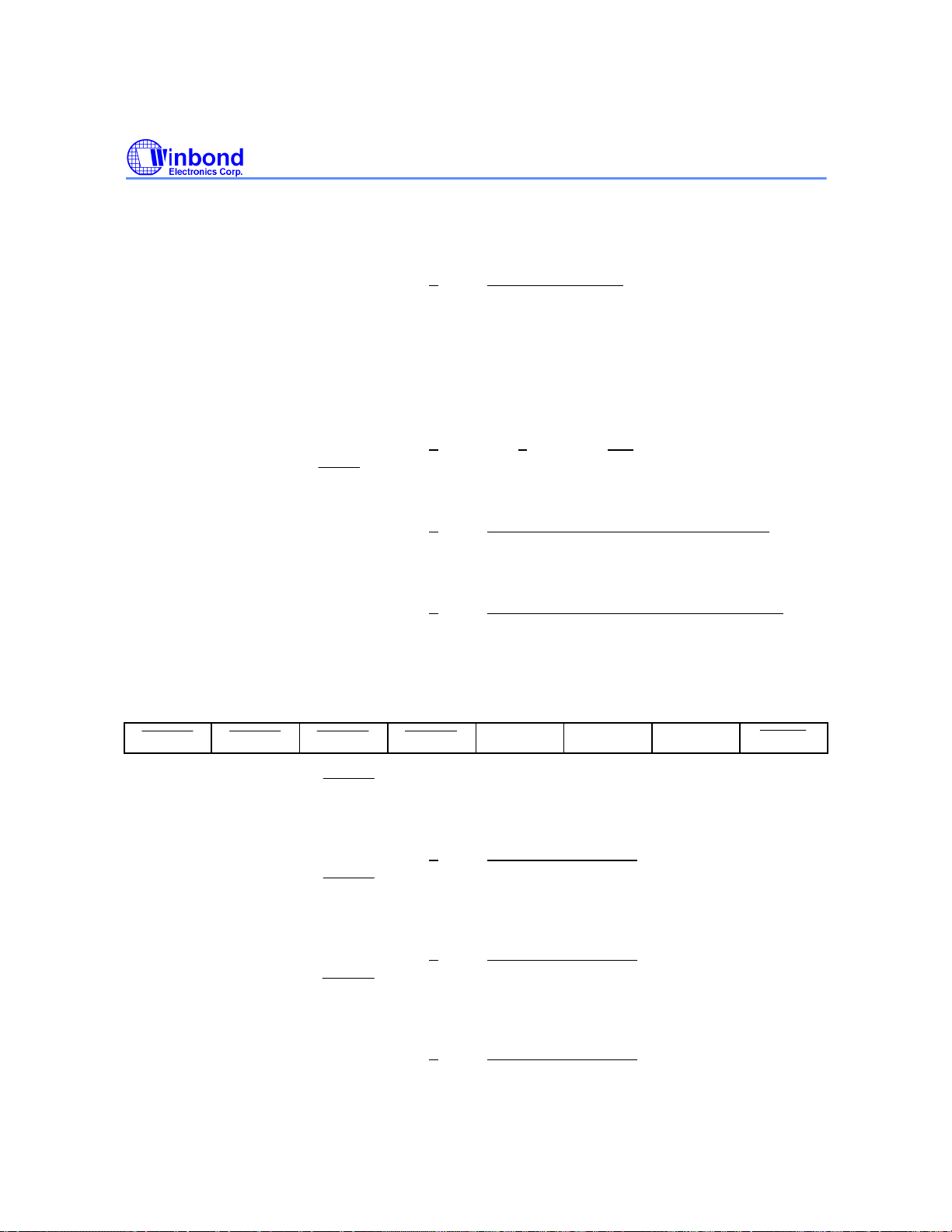
Continued
CRLK
PD0EM
PD1EM
SD0EM
SD1EM
SWAP
PD0EM
PD1EM
SD0EM
W83759A
Bit 4 SD1LEN_P Secondary Drive 1(SD1) local device control
0 Disable local device
1 Enable local device
Bit 3, 2 DSL1, 0_P Device ID selection (used in multi-chip mode or CR
protection scheme)
DSL1_P DSL0_P Device ID
0 0 60h
0 1 61h
1 0 62h
1 1 63h
Bit 1
Bit 0 CRSL_P Configuration Register selection
CRX84h (POSS3) Read Only Power-on Setting Status 3
Bit 7 Bit 6 Bit 5 Bit 4 Bit 3 Bit 2 Bit 1 Bit 0
Bit 7
Bit 6
_P
Configuration Register locked control
0 CR is auto-locked (multi-chip mode)
1 CR is not auto-locked (single-chip mode)
0 CR port address: 130h, 134h, 138h, 13Ch
1 CR port address: 1B0h, 1B4h, 1B8h, 1BCh
SUSPEN STBY# APD
Power-on setting value of IDD15 pin
Initial setting of PD0 enhanced timing enable
0 Enhanced timing
1 Programmable timing
Power-on setting value of IDD14 pin
Initial setting of PD1 enhanced timing enable
0 Enhanced timing
1 Programmable timing
Bit 5
Power-on setting value of IDD13 pin
Initial setting of SD0 enhanced timing enable
0 Enhanced timing
1 Programmable timing
- 16 -
Page 17

Continued
SD1EM
DMASL
DMASL
STBY
SWAP
PD0EM
Bit 4
Power-on setting value of IDD12 pin
Initial setting of SD1 enhanced timing enable
0 Enhanced timing
1 Programmable timing
Bit 3 SUSPEN Power-on setting value of IDD11 pin
Initial setting of SUSPend function
W83759A
0 Support DMA mode if
ADV_P = 1
1 Support suspend function if
and ADV_P = 1.
Bit 2
Power-on setting value of IDD10 pin
Initial setting of STandBy state
0 W83759A is in standby state
1 W83759A is in normal state
Bit 1 APD Power-on setting value of IDD9 pin
Initial setting of auto Power-down
0 Auto power-down off
1 Auto power-down on
Bit 0
Power-on setting value of IDD8 pin
Initial primary, secondary channel connection select
0 Primary channel connect to IDE1
Secondary channel connect to IDE0
1 Primary channel connect to IDE0
Secondary channel connect to IDE1
_P = 0 and
_P = 0
CRX85h (POSP3) Read/ Write Power-on Setting Programming 3
Bit 7 Bit 6 Bit 5 Bit 4 Bit 3 Bit 2 Bit 1 Bit 0
PD0EM _P PD1EM _P SD0EM_P SD1EM_P
Bit 7
_P
Power-on setting programming of IDD15 pin
SUSPEN_P
STBY _P
APD_P
Programmable setting of PD0 enhanced timing enable
0 Enhanced timing
1 Programmable timing
Publication Release Date: May 1995
- 17 - Revision A1
SWAP _P
Page 18

Continued
PD1EM
SD0EM
SD1EM
DMASL
DMASL
STBY
SWAP
Bit 6
_P
W83759A
Power-on setting programming of IDD14 pin
Programmable setting of PD1 enhanced timing enable
0 Enhanced timing
1 Programmable timing
Bit 5
Bit 4
Bit 3 SUSPEN_P Power-on setting value of IDD11 pin
Bit 2
Bit 1 APD_P Power-on setting value of IDD9 pin
_P
_P
_P
Power-on setting programming of IDD13 pin
Programmable setting of SD0 enhanced timing enable
0 Enhanced timing
1 Programmable timing
Power-on setting programming of IDD12 pin
Programmable setting of SD1 enhanced timing enable
0 Enhanced timing
1 Programmable timing
Programmable setting of SUSPend function
0 Support suspend function if
and ADV_P = 1
1 Support DMA transfer if
and ADV_P = 1
Power-on setting value of IDD10 pin
Programmable setting of STandBy state
0 W83759A is in standby state
1 W83759A is in normal state
Initial setting of auto power-down
0 Auto power-down off
1 Auto power-down on
_P = 0
_P = 0
Bit 0
_P
Power-on setting programming of IDD8 pin
Programmable primary, secondary channel connection
select
0 Primary channel connect to IDE1
Secondary channel connect to IDE0
1 Primary channel connect to IDE0
Secondary channel connect to IDE1
- 18 -
Page 19
Continued
DMASL
DMASL
VGAOEL
IDEIOR
IDEIOW
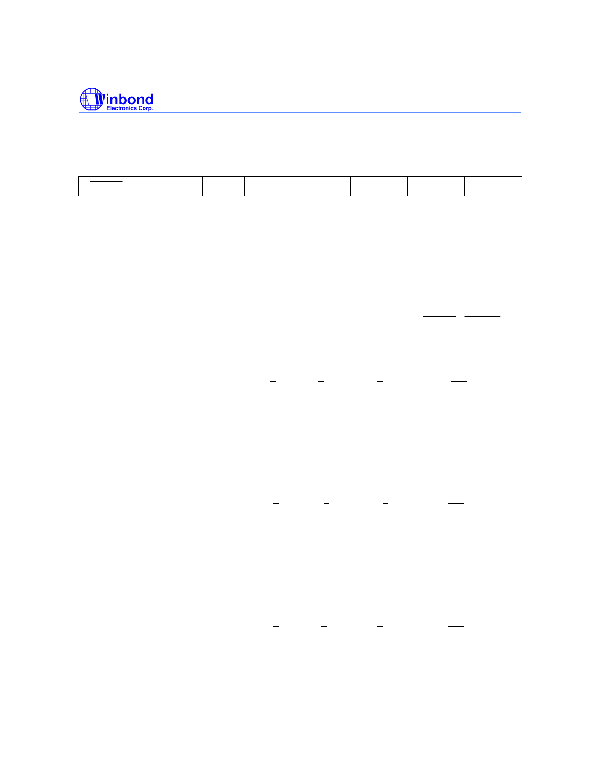
CRX86h (ALTCTL) Read / Write Alternative Control Register
Bit 7 Bit 6 Bit 5 Bit 4 Bit 3 Bit 2 Bit 1 Bit 0
Reserved EMD1 EMD0 PEMD1_P PEMD0_P SEMD1_P SEMD0_P
_P
W83759A
Bit 7
Bit 6 Reserved 0 (default)
Bit5−4
Bit3−2
EMD1, 0
(Read Only)
PEMD1, 0_P Initial setting of primary drive enhanced timing
_P Power-on setting value of
After power-on, this bit can be programmed to modify
the DMA disable/enable power-on setting.
0 DMA mode enabled if SUSPEN_P = 0 and
ADV_P = 1
1 DMA mode disabled
Inverse of power-on setting value of
pin
Initial setting of enhanced timing of IDE0 and IDE1
EMD1 EMD0 ATA PIO Mode Cycle time (nS)
0 0 2 240
0 1 3 80
1 0 3 80
1 1 4 120
After power-on, these bits can be programmed to modify
the primary drive enhanced timing.
PEMD1_P PEMD0_P ATA PIO mode Cycle time (nS)
0 0 2 240
0 1 3 180
1 0 3 180
1 `1 4 120
pin.
,
Bit1−0
SEMD1, 0_P Initial setting of secondary drive enhanced timing
After power-on, these bits can be programmed to modify
the secondary drive enhanced timing
SEMD1_P SEMD0_P ATA PIO Mode Cycle time (nS)
0 0 2 240
0 1 3 180
1 0 3 180
1 1 4 120
Publication Release Date: May 1995
- 19 - Revision A1
Page 20

W83759A
DMASL
DMASL
VGAOEL
CRX87h (REVID) Read Only Revision ID Number
Bit 7 Bit 6 Bit 5 Bit 4 Bit 3 Bit 2 Bit 1 Bit 0
Reserved PDRV SDRV Rev 3 Rev 2 Rev 1 Rev 0
Bit 7
Bit 6 Reserved
(Read/Write)
Bit 5 PDRV Primary channel current drive select
Bit 4 SDRV Secondary channel current drive select
Bit 3-Bit 0 Rev 3−Rev 0 1010b (default in A version)
Power-on setting value of
Initial DMA enable/disable setting
0 DMA mode enabled if SUSPEN_P = 0 and
ADV_P = 1
1 DMA mode disabled
0 (default)
0 Master drive (default)
1 Slave drive
0 Master drive (default)
1 Slave drive
pin.
- 20 -
Page 21

W83759A
CRX88h (PD0TIM0) Read/Write Primary Drive0 Timing Control 0
Bit 7 Bit 6 Bit 5 Bit 4 Bit 3 Bit 2 Bit 1 Bit 0
PD0ACT3 PD0ACT2 PD0ACT1 PD0ACT0 PD0RCV3 PD0RCV2 PD0RCV1 PD0RCV0
Bit 7−Bit 4 PD0ACT3−0
Bit 3−Bit 0 PD0RCV3−0
PD0 Data Register Port (1F0h) Read/Write Active Time
Read/Write active time (clocks)
0000 17/16
0001 3/2
0010 3/2
0011 4/3
0100 5/4
0101 6/5
0110 7/6
0111 8/7
1000 9/8
1001 10/9
1010 11/10
1011 12/11
1100 13/12
1101 14/13
1110 15/14
1111 16/15
PD0 Data Register Port (1F0h) Read/Write Recovery
Time
Write/Read recovery time (clocks)
0000 16/15
0001 2/1
0010 2/1
0011 3/2
0100 4/3
0101 5/4
0110 6/5
0111 7/6
1000 8/7
1001 9/8
1010 10/9
1011 11/10
1100 12/11
1101 13/12
1110 14/13
1111 15/14
Publication Release Date: May 1995
- 21 - Revision A1
Page 22
W83759A
PD0PRE
PD0DMA
PD0RDY
PD0PRE
PD0DMA
PD0RDY
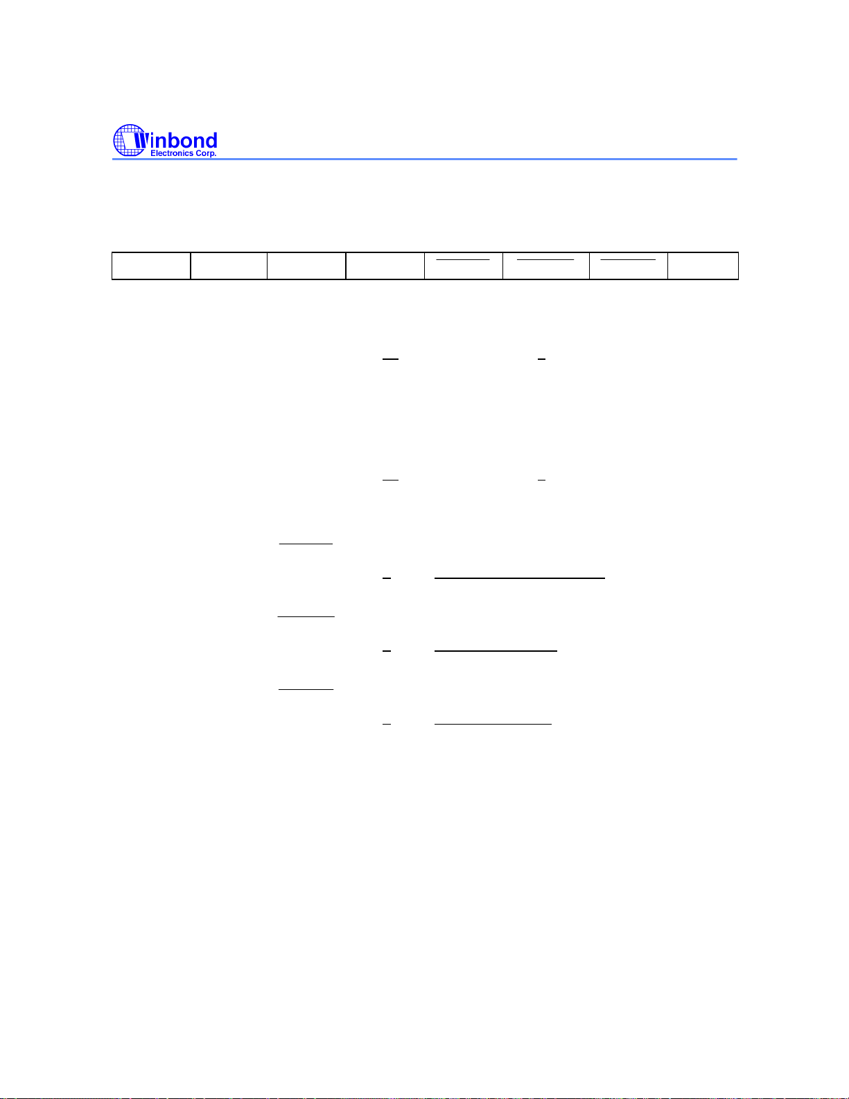
CRX89h (PD0TIM1) Read/Write Primary Drive0 Timing Control 1
Bit 7 Bit 6 Bit 5 Bit 4 Bit 3 Bit 2 Bit 1 Bit 0
PD0AST1 PD0AST0 PD0DHT1 PD0DHT0
Bit 7−Bit 6 PD0AST1−0
Bit 5−Bit 4 PD0DHT1−0
Bit 3
Bit 2
PD0 Data Register Port (1F0h) Address Setup Time
Read/Write extra address setup time (clocks)
00 0
01 2
10 2
11 3
PD0 Data Register Port (1F0h) Data Hold Time
Read/Write extra data hold time (clocks)
00 0
01 2
10 2
11 3
Prefetch/Post write control
0 Prefetch/Post write enabled
1 Prefetch/Post write disabled
PD0 DMA mode control
0 DMA mode enabled
1 DMA mode disabled
PD0ADV
Bit 1
Bit 0 PD0ADV PD0 Data Register Port (1F0h) Advanced Timing
PD0 Data Register Port (1F0h) IOCHRDY Control
0 IOCHRDY enabled
1 IOCHRDY disabled
Enable
0 Normal timing (depends on SP1, MD1, MD0
setting)
1 Advanced timing (depends on PD0TIM1−0
setting)
- 22 -
Page 23
W83759A
PD1PRE
PD1DMA
PD1RDY
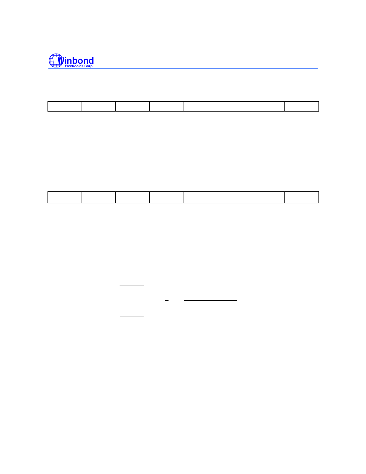
CRX8Ah (PD1TIM0) Read/Write Primary Drive1 Timing Control 0
Bit 7 Bit 6 Bit 5 Bit 4 Bit 3 Bit 2 Bit 1 Bit 0
PD1ACT3 PD1ACT2 PD1ACT1 PD1ACT0 PD1RCV3 PD1RCV2 PD1RCV1 PD1RCV0
Bit 7−Bit 4 PD1ACT3−0
Bit 3−Bit 0 PD1RCV3−0
CRX8Bh (PD1TIM1) Read/Write Primary Drive 1 Timing Control 1
Bit 7 Bit 6 Bit 5 Bit 4 Bit 3 Bit 2 Bit 1 Bit 0
PD1AST1 PD1AST0 PD1DHT1 PD1DHT0
Bit 7-Bit 6
Bit 5-Bit 4
Bit 3
Bit 2
PD1AST1−0
PD1DHT1−0
PD1 Data Register Port (1F0h) Read/Write Active Time
Definition of these bits same as PD0ACT3−0
PD1 Data Register Port (1F0h) Read/Write Recovery Time
Definition of these bits same as PD0RCV3−0
PD1PRE PD1DMA PD1RDY
PD1 Data Register Port (1F0h) Address Setup Time
Definition of these bits same as PD0AST1-0
PD1 Data Register Port (1F0h) Data Hold Time
Definition of these bits same as PD0DHT1−0
PD1 Prefetch/Post write control
0 Prefetch/Post write enabled
1 Prefetch/Post write disabled
PD1 DMA mode control
0 DMA mode enabled
1 DMA mode disabled
PD1ADV
Bit 1
Bit 0 PD1ADV PD1 Data Register Port (1F0h) Advanced Timing Enable
PD1 Data Register Port (1F0h) IOCHRDY Control
0 OCHRDY enabled
1 IOCHRDY disabled
0 Normal timing (depends on SP1, MD1, MD0
setting)
1 Advanced timing (depends on PD1TIM1−0 setting)
Publication Release Date: May 1995
- 23 - Revision A1
Page 24
W83759A
SD0PRE
SD0DMA
SD0RDY
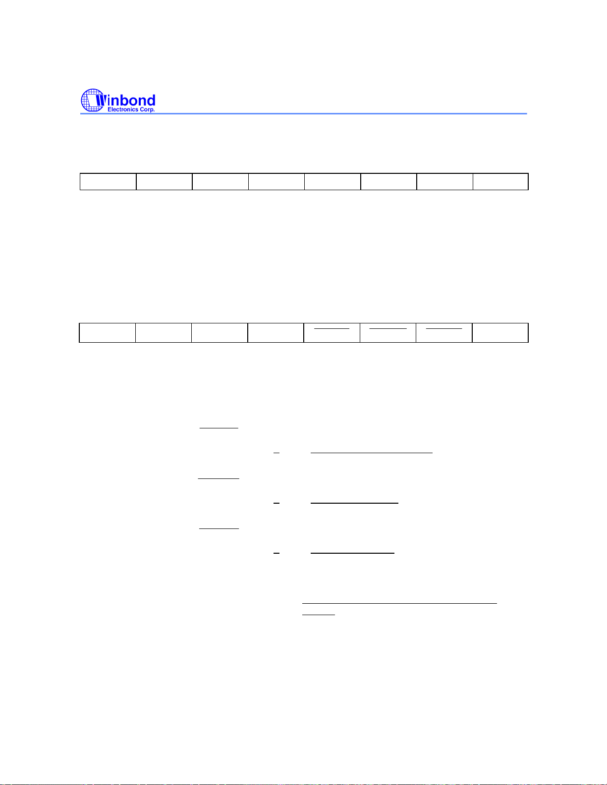
CRX8Ch (SD0TIM0) Read/Write Secondary Drive 0 Timing Control 0
Bit 7 Bit 6 Bit 5 Bit 4 Bit 3 Bit 2 Bit 1 Bit 0
SD0ACT3 SD0ACT2 SD0ACT1 SD0ACT0 SD0RCV3 SD0RCV2 SD0RCV1 SD0RCV0
Bit 7-Bit 4
Bit 3-Bit 0
CRX8Dh (SD0TIM1) Read/Write Secondary Drive 0 Timing Control 1
Bit 7 Bit 6 Bit 5 Bit 4 Bit 3 Bit 2 Bit 1 Bit 0
SD0AST1 SD0AST0 SD0DHT1 SD0DHT0
Bit 7-Bit 6
Bit 5-Bit 4
Bit 3
Bit 2
SD0ACT3−0
SD0RCV3−0
SD0AST1−0
SD0DHT1−0
SD0 Data Register Port (170h) Read/Write Active Time
Definition of these bits same as PD0ACT3−0
SD0 Data Register Port (170h) Read/Write Recovery Time
Definition of these bits same as PD0RCV3−0
SD0PRE SD0DMA SD0RDY
SD0 Data Register Port (170h) Address Setup Time
Definition of these bits same as PD0AST1−0
SD0 Data Register Port (170h) Data Hold Time
Definition of these bits same as PD0RDHT1−0
SD0 Prefetch/Post write control
0 Prefetch/Post write enabled
1 Prefetch/Post write disabled
SD0 DMA mode control
0 DMA mode enabled
1 DMA mode disabled
SD0ADV
Bit 1
Bit 0 SD0ADV SD0 Data Register Port (170h) Advanced Timing Enable
SD0 Data Register Port (170h) IOCHRDY Control
0 IOCHRDY enabled
1 IOCHRDY disabled
0 Normal timing (depends on SP1, MD1, MD0
setting)
1 Advanced timing (depends on SD0TIM1−0 setting)
- 24 -
Page 25
W83759A
SD1PRE
SD1DMA
SD1RDY
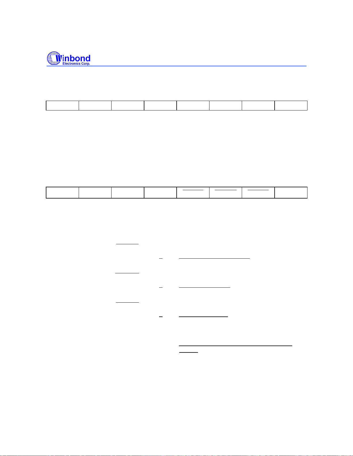
CRX8Eh (SD1TIM0) Read/Write Secondary Drive 1 Timing Control 0
Bit 7 Bit 6 Bit 5 Bit 4 Bit 3 Bit 2 Bit 1 Bit 0
SD1ACT3 SD1ACT2 SD1ACT1 SD1ACT0 SD1RCV3 SD1RCV2 SD1RCV1 SD1RCV0
Bit 7−Bit 4 SD1ACT3−0
Bit 3−Bit 0 SD1RCV3−0
CRX8Fh (SD1TIM1) Read/Write Secondary Drive 1 Timing Control 1
Bit 7 Bit 6 Bit 5 Bit 4 Bit 3 Bit 2 Bit 1 Bit 0
SD1AST1 SD1AST0 SD1DHT1 SD1DHT0
Bit 7−Bit 6 SD1AST1−0
Bit 5−Bit 4 SD1DHT1−0
Bit 3
Bit 2
SD1 Data Register Port (170h) Read/Write Active Time
Definition of these bits same as PD0RCV3-0
SD1 Data Register Port (170h) Read/Write Recovery Time
Definition of these bits same as PD0RCV3-0
SD1PRE SD1DMA SD1RDY
SD1 Data Register Port (170h) Address Setup Time
Definition of these bits same as PD0RCV3−0
SD1 Data Register Port (170h) Data Hold Time
Definition of these bits same as PD0RCV3−0
SD1 Prefetch/Post write control
0 Prefetch/Post write enabled
1 Prefetch/Post write disabled
SD1 DMA mode control
0 DMA mode enabled
1 DMA mode disabled
SD1ADV
Bit 1
Bit 0 SD1ADV SD1 Data Register Port (170h) Advanced Timing Enable
SD1 Data Register Port (170h) IOCHRDY Control
0 IOCHRDY enabled
1 OCHRDY disabled
0 Normal timing (depends on SP1, MD1, MD0
setting)
1 Advanced timing (depends on SD1TIM1−0 setting)
Publication Release Date: May 1995
- 25 - Revision A1
Page 26
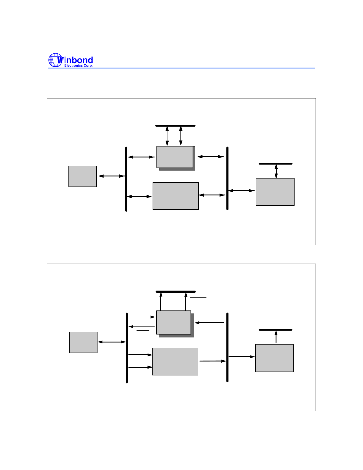
SYSTEM BLOCK DIAGRAM
Data Flow
HD
IDE ATA Bus x 2
IDD
VL_IDE
W83759AF
(100-pin)
SD
W83759A
IO Device
CPU
Address Decode
CPU
HD
HD
VL_BUS ISA Bus
IDE0CS
HA
LDEV
HA
HA
LDEV
VL-Bus
Chip Set
W83C491/492
(160-pin x2)
IDE ATA Bus x 2
IDEA[2:0]
VL_IDE
W83759AF
(100-pin)
VL-Bus
Chip Set
W83C491/492
(160-pin x2)
SD
IDE1CS
SA
SA
SD
SA
Super IO
W83787F
(100-pin)
IO Device
Super IO
W83757
W83787F
(100-pin)
VL_BUS ISA Bus
- 26 -
Page 27
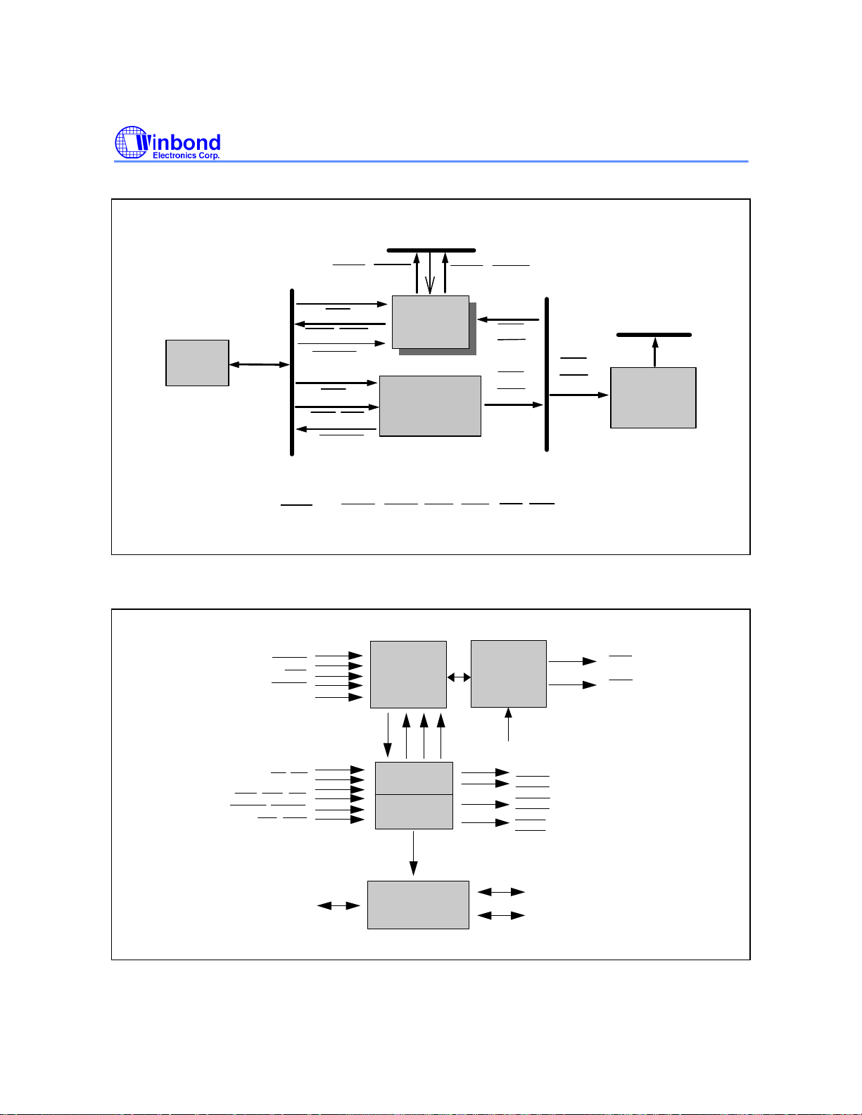
Control Signal
W83759A
IDE ATA Bus x 2
IDEIOR, IDEIOW
LADS, ... *
LDEV, LRDY
CPU
RDYRTN
LADS,...
LDEV, LRDY
RDYRTN
VL_BUS
* LADS,... = LADS, HMIO, HWR, HDC, BE2, BE0
FUNCTION BLOCK DIAGRAM
LCLK
SYSRST
LADS
RDYRTN
SP1, MD1, MD0
IORDY
VL_IDE
W83759AF
(100-pin)
VL-Bus
Chip Set
W83C491/492
(160-pin x2)
TIMING
REGISTERS
MUX
IDEIOR, IDEIOW
XIOR
XIOW
XIOR
XIOW
CONTROL
LOGIC
ISA Bus
XIOR
XIOW
IO Device
Super IO
W83787F
(100-pin)
LRDY
LDEV
HA[9:2]
BE2, BE0
SA1, SA0, AEN
HMIO, HWR, HDC
VGAOEH, VGAOEL
XIOR, XIOW
HD[31:0]
Command
Enable
16
1f0
32
/170
Bit
Bit
DECODE
LOGIC
PREFETCH
CONTROL
Data Flow
Control
DATA
BUFFER
IORDY
IDEA[2:0]
IDE0CS1
IDE0CS0
IDE1CS1
IDE1CS0
IDEIOR
IDEIOW
ID[15:0]
SD[7:0]
Publication Release Date: May 1995
- 27 - Revision A1
Page 28
W83759A
SYSRST
SYSRST
SYSRST
HMIO
HDC
HWR
BE3
BE2
BE1
BE0
FUNCTIONAL DESCRIPTION
Reset Initialization
The CPU clock rate, hard disk access time, hard disk controller enable, and hard disk I/O select are
latched at the rising edge of
signal timing. Additionally, the W83759A is initialized to a known state by an active low on
Any operation in progress is immediately terminated by
Host in Terface
The W83759A operates as a slave device, responding only to cycles within the host I/O address
space. The IDE drive data port at address 1F0h (170h) is a 16-bit port that requests a double-word
data transfer at address 1F0h (170h). All byte swapping, conversion, word, and double-word assembly
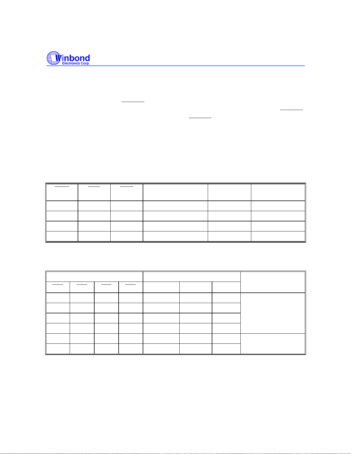
are done at the host interface. Table 1 summarizes the W83759A host interface cycle decoding.
Table 1. W83759A Cycle Definition
. These values are used to control the host and drive access
.
.
ADDRESS SPACE HOST BUS
0 1 0
0 1 1
0 1 0
0 1 1
a. CPU WRITE CYCLES
Table 2. W83759A Write Data Operation
BYTE ENABLE W83759A INPUT DATA I/O ADDRESS
1 1 1 0
1 1 0 1
1 0 1 1
0 1 1 1
1 1 0 0
0 0 0 0 Valid Valid
1F0h−1F7h and 3F6h
1F0h−1F7h and 3F6h
170h−177h and 376h
170h−177h and 376h
HD[31:16] HD[15:0] SD[7:0]
× ×
× ×
× ×
× ×
×
Valid
W83759A CYCLE
CYCLE
I/O Read IDE0 Read Cycle
I/O Write IDE0 Write Cycle
I/O Read IDE1 Read Cycle
I/O Write IDE1 Write Cycle
Valid
Valid
Valid
Valid
×
×
1F1−1F7 (171−177)
1F0 (170)
8-bit IDE Write Data Path:
CPU → Valid HD Byte → SD[7:0] → W83759A → ID[7:0]
16/32-bit IDE Write Data Path:
CPU → Valid HD Word → W83759A → ID[15:0]
- 28 -
Page 29
W83759A
BE3
BE2
BE1
BE0
IDE0CS0
IDE1CS
0
IDE0CS1
IDE1CS1
IDEIOR
IDEIOW
BE2, BE0
BE2
BE0
IDE0CS0
IDE1CS0
IDE0CS1
IDE1CS1
IDEIOR
IDEIOW
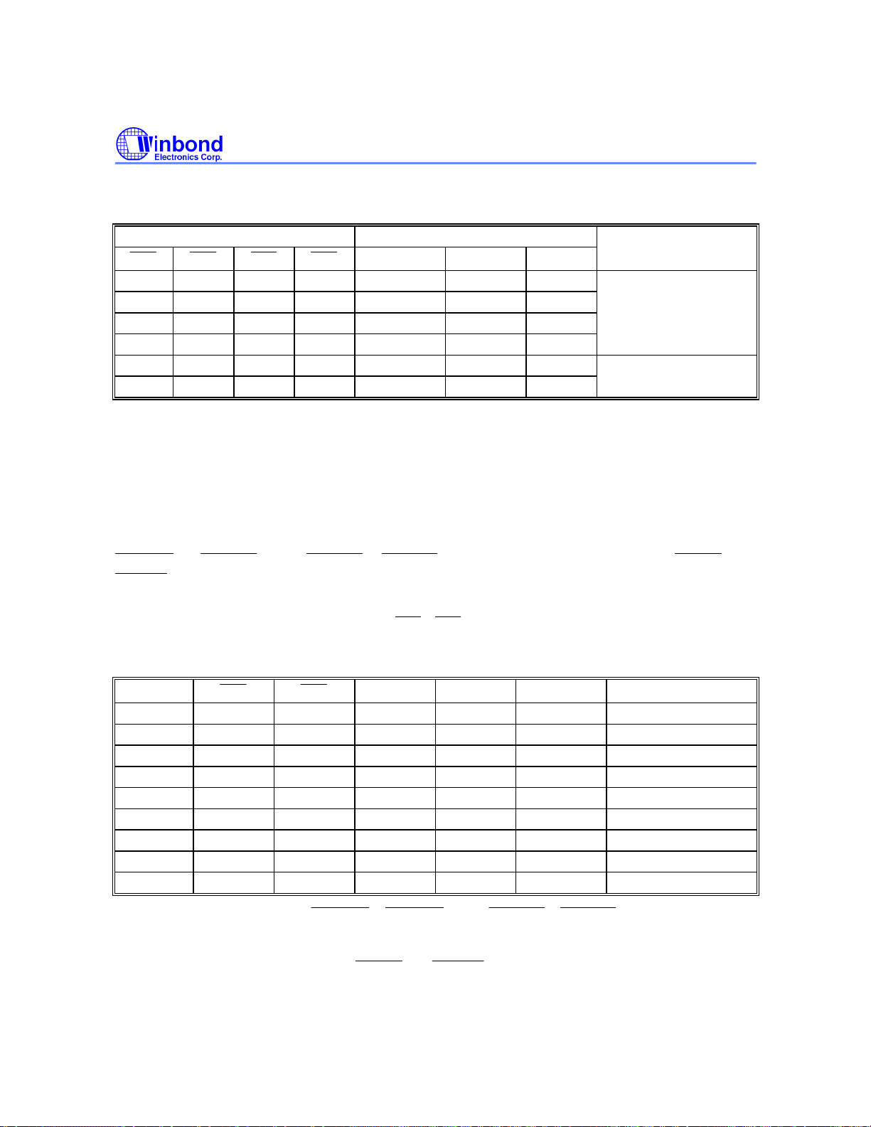
b. CPU READ CYCLES
Table 3. W83759A Read Data Operation
BYTE ENABLE W83759A OUTPUT DATA I/O ADDRESS
HD[31:16] HD[15:0] SD[7:0]
1 1 1 0
1 1 0 1
1 0 1 1
0 1 1 1
1 1 0 0
× ×
× ×
× ×
× ×
×
Valid
0 0 0 0 Valid Valid
8-bit IDE Read Data Path:
CPU → Valid HD Byte → Chip Set → SD[7:0] → W83759A → ID[7:0]
16/32-bit IDE Read Data Path:
CPU → Valid HD Word → W83759A → ID[15:0]
Drive Interface
The W83759A is designed to work with standard IDE disk drives. For the IDE interface, the W83759A
provides a 16-bit data path ID[15;0], address lines IDEA[2:0], decoded device select signals
(
.
During normal operation, the drive address outputs IDEA[2:0] are used to select a register in an IDE
drive. These addresses are generated from
type enable decoding for normal operation.
Table 4. IDEA[2:0] Generation
) and
(
), and decoded command sigals
, HA2 and SA1, SA0. Table 4 summarizes the
Valid
Valid
Valid
Valid
×
×
1F1−1F7 (171−177)
1F0 (170)
and
HA2
0 1 0
0 0 0
0
0
0
1
1
1
1
× ×
× ×
× ×
× ×
× ×
× ×
× ×
Two drive chip select signals,
SA1 SA0 IDEA[2:0] I/O ADDRESS
× ×
× ×
000 1F0 (170) 16-bit
000 1F0 (170) 32-bit
0 1 001 1F1 (171)
1 0 010 1F2 (172)
1 1 011 1F3 (173)
0 0 100 1F4 (174)
0 1 101 1F5 (175)
1 0 110 1F6 (176)
1 1 111 1F7 (177)
(
) and
(
), are generated from
the local bus addresses and ISA bus address. The 16-bit data register may be read or written at I/O
address 1F0h(170h). The 8-bit IDE command and status registers are at I/O addresses 1F1h through
1F7h (and 171h through 177h). The
or
commands are generated for all address
Publication Release Date: May 1995
- 29 - Revision A1
Page 30
W83759A
IDE0CS
0
IDE1CS0
IDE0CS
1
IDE1CS1
IDE0CS0
IDE0CS1
IDE1CS0
IDE1CS1
XIOR
XIOW
regions in which
decoding of these sgnals.
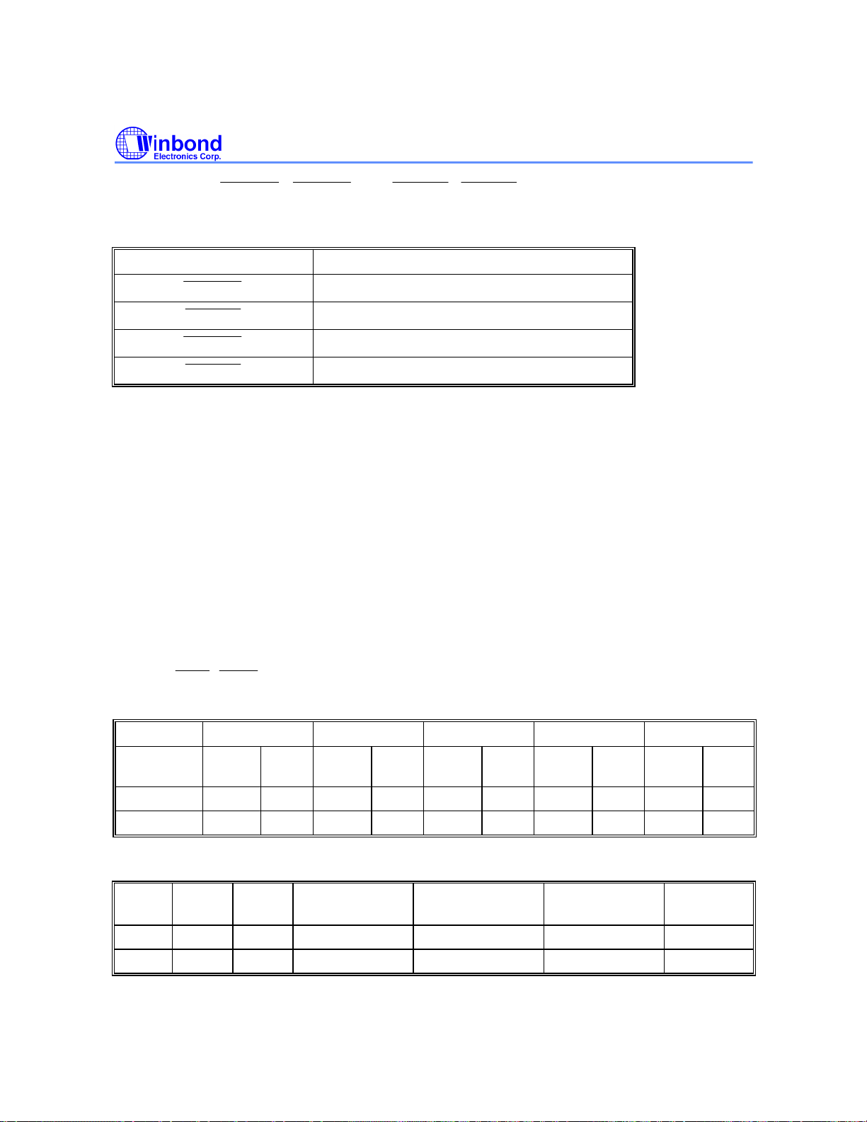
Table 5. Drive Select Signal Operation
SELECT SIGNAL ADDRESS RANGE
(
) and
I/O Address 1F0h through 1F7h
I/O Address 3F6h
I/O Address 170h through 177h
I/O Address 376h
(
) are active. Table 5 summarizes the
IDE Timing Control
Pin SP1 is used to set the VL-Bus speed. The IDE drive interface will maintain the same ATA PIO
timing parameters for IDE drive 16-bit IO access cycles (1F0/170) regardless of whether the VL-Bus
operates at 33 or 50 MHz.
In W83759 mode, IDE drive timing is controlled by pins MD1 and MD0, which are used to select the
IDE drive PIO mode 0-2. The drive timing depends on the ATA specification for the IDE drive PIO
mode selected.
In W83759A mode, IDE drive timing is controlled by pins EMD1 and EMD0, which are used to select
the IDE drive PIO mode 2-4. The drive timing depends on the ATA specification for the IDE drive PIO
mode selected.
Table 6 summarizes the ATA Rev. 4.0 and ATA-2 PIO timing parameters.
Table 7 and Table 8 summarize the W83759A PIO read/write command pulse and cycle timing when
a 16-bit IDE IO access is performed. Because 8-bit IDE IO accesses are always passed to the ISA
bus, the W83759A transceives data through the ISA data bus and induces IDE read/write commands
from ISA
/
. Thus the 8-bit command timing will always meet ATA timing specifications.
Table 6. ATA Rev. 4.0 and ATA-2 PIO Minimum Timing Parameters Unit: nS
ATA PIO MODE 4 MODE 3 MODE 2 MODE 1 MODE 0
8/16-bit IO
access
16-bit 60 120 80 180 100 240 125 383 165 600
8-bit 60 120 80 180 290 290 290 383 290 600
Table 7. PIO Command Pulse and Cycle Timing (W83759 mode) Unit: LCLK
SP1 MD1 MD0 IDE WRITE
0 0 0 6 (180) 7 (210) 22 (660) Mode 0
0 0 1 6 (180) 7 (210) 19 (570) Mode 0+
Active
Pulse
Cycle
Time
Active
Pulse
ACTIVE PULSE
Cycle
Time
Active
Pulse
IDE READ
ACTIVE PULSE
- 30 -
Cycle
Time
Active
Pulse
Cycle
Time
READ/WRITE
CYCLE TIME
Active
Pulse
IDE MODE
SELECT
Cycle
Time
Page 31
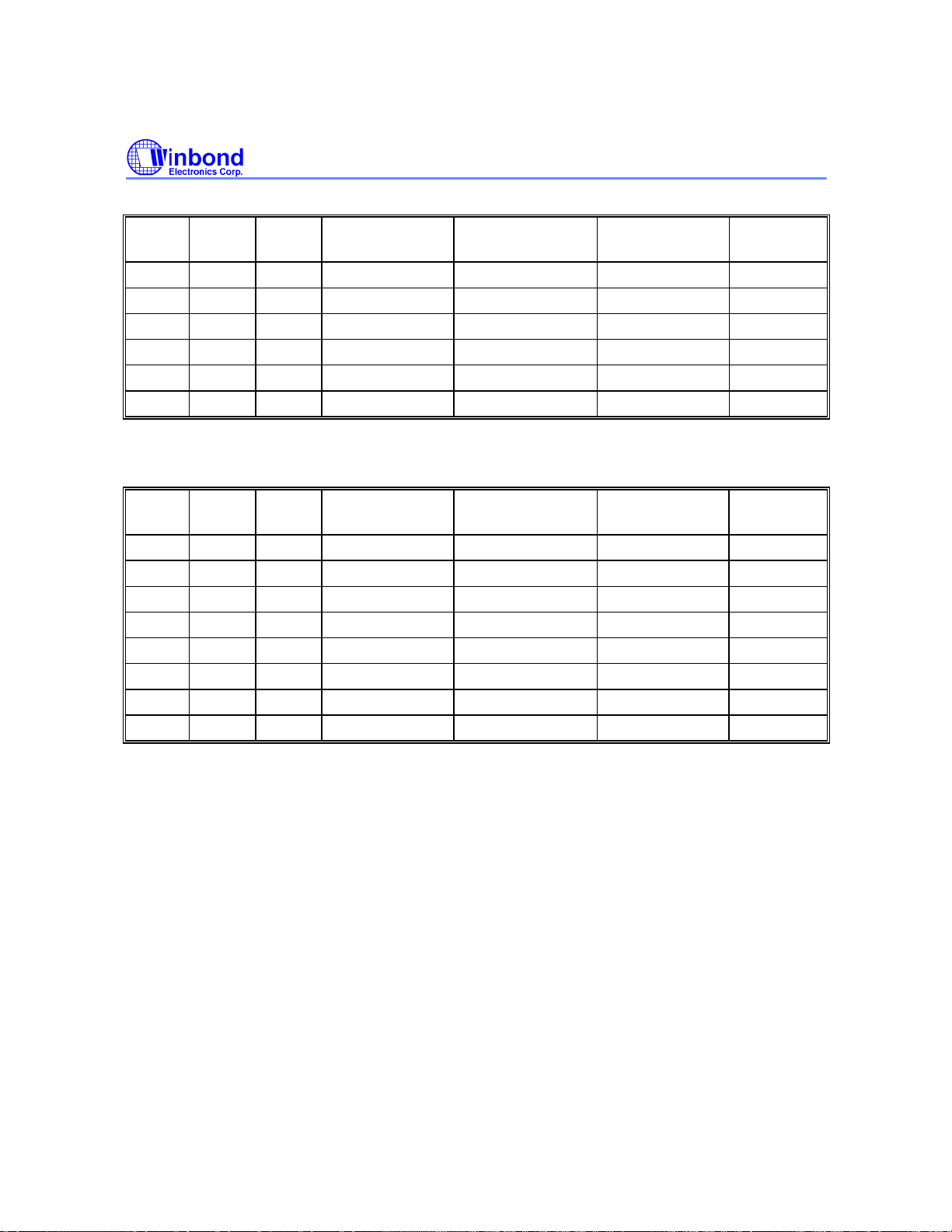
Table 7. PIO Command Pulse and Cycle Timing, continued
W83759A
SP1 MD1 MD0 IDE WRITE
ACTIVE PULSE
IDE READ
ACTIVE PULSE
READ/WRITE
CYCLE TIME
IDE MODE
SELECT
0 1 0 8 (240) 9 (270) 13 (390) Mode 1
0 1 1 4 (120) 5 (150) 9 (270) Mode 2
1 0 0 9 (180) 10 (200) 31 (620) Mode 0
1 0 1 9 (180) 10 (200) 27 (540) Mode 0+
1 1 0 7 (140) 8 (160) 19 (380) Mode 1
1 1 1 6 (120) 7 (140) 13 (260) Mode 2
Note: It is recommended that SP be set to 0 when LCLK is 33 MHz. The initial default value is SP1 = 0. The timing value (nS) is
based on LCLK = 20 nS when SP1 = 1 and LCLK = 30 nS when SP1 = 0.
Table 8. PIO Command Pulse and Cycle Timing (W83759A mode) Unit: LCLK
SP1 EMD1 EMD0 IDE WRITE
ACTIVE PULSE
IDE READ
ACTIVE PULSE
READ/WRITE
CYCLE TIME
IDE MODE
SELECT
0 0 0 4 (120) 5 (150) 8 (240) Mode 2
0 0 1 3 (90) 4 (120) 6 (180) Mode 3
0 1 0 3 (90) 4 (120) 6 (180) Mode 3
0 1 1 2 (60) 3 (90) 4 (120) Mode 4
1 0 0 4 (80) 5 (100) 11 (220) Mode 2
1 0 1 4 (80) 5 (100) 9 (180) Mode 3
1 1 0 3 (60) 4 (80) 7 (140) Mode 41 1 1 2 (40) 3 (60) 5 (100) Mode 4+
Note: It is recommended that SP be set to 0 when LCLK is 33 MHz. The initial default value is SP1 = 0. The timing value (nS) is
based on LCLK = 20 nS when SP1 = 1 and LCLK = 30 nS when SP1 = 0.
Prefetch Control
The W83759A IDE command prefetch feature provides concurrent operations by pipelined readahead of the next data word(s) from the drive while the host is transferring previously requested disk
data into system memory. This reduces the amount of time that the host must pause and wait for data
to be accessed. While the host is writing data to memory, the W83759A reads data from the disk
drive. As soon as the host reads the W83759A data, new data are requested by the W83759A from
the disk drive. This prefetch feature is active only for disk data at the 1F0h and 170h IO addresses
and does not oprate on other disk register data.
Power-saving Control
The W83759A provides three power-saving modes. In the initial-level power-saving mode, all of the
drive's control, address, data, and other signals enter a logic 1 standby state when no IDE disk cycle
is active. This reduces unnecessary power use and decreases the amount of EMI radiation generated
by driving the long IDE cable continuously.
Publication Release Date: May 1995
- 31 - Revision A1
Page 32
W83759A
STBY
STBY
DMASL
SYSRST
SUSP
SUSP
LDEV
LDEV
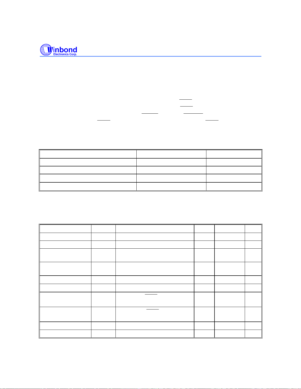
After power on, the W83759A automatically enters the "Auto-Power-Down" (APD) mode. In this mode
the only active logic inside the W83759A is the host address decoder and bus tracking state machine.
Power is saved by not switching logic inside the W83759A that is not being utilized. Whenever an IDE
transfer cycle is detected, the W83759A leaves APD mode and the entire chip becomes active. The
W83759A enters APD mode again after the completion of an IDE transfer cycle.
To support deep-green systems, the W83759A also provides advanced power saving modes, standby
mode, and suspend mode. When standby mode is enabled (
inside the W83759A is stopped until standby mode is disabled (
mode is enabled (SUSPEN bit goes high and
enter suspend state when
goes low and return to normal state when
is low on
ABSOLUTE MAXIMUM RATINGS
(VDD = 5 V ± 5%, VSS = 0V )
PARAMETER RATING UNIT
Power Supply Voltage -0.3 to 7.0 V
Input Voltage VSS-0.3 to VDD +0.3 V
Operating Temperature (Ta) 0 to + 70
Storage Temperature -55 to + 150
Note: Exposure to conditions beyond those listed under Absolute Maximum Ratings may adversely affect the life and reliability of the
device.
bit goes low), all of the logic
bit goes high). When suspend
rising), the W83759A will
goes high.
°C
°C
DC CHARACTERISTICS
(TA = 0° C to +70° C, VDD = 5V ± 5%, VSS = 0V)
PARAMETER SYM. CONDITIONS MIN. MAX. UNIT
Input Low Voltage VIL -0.3 0.8 V
Input High Voltage VIH 2.0 VDD + 0.3 V
Input High Leakage
with Pull-Down
Input Low Leakage
with Pull-Up
Input High Leakage ILIH VIN = VDD - +10
Input Low Leakage ILIL VIN = 0V - -10
Output Low Voltage VOL
Output High Voltage VOH
Input Capacitance CIN - 5 pF
Output Capacitance COUT - 10 pF
ILIHD VIN = VDD - +500
ILILU VIN = 0V - -500
IOL = 8 mA (
IOL = 6 mA (other pins)
IOL = -8 mA (
IOL = -6 mA (other pins)
, SD, IDE pins)
, SD, IDE pins)
- 0.4 V
2.4 VDD V
µA
µA
µA
µA
- 32 -
Page 33
W83759A
SYSRST
SYSRST
SYSRST
LADS
LADS
LDEV
HMIO
HDC
HWR
LDEV
HMIO
HDC
HWR
LDEV
LRDY
LRDY
RDYRTN
RDYRTN
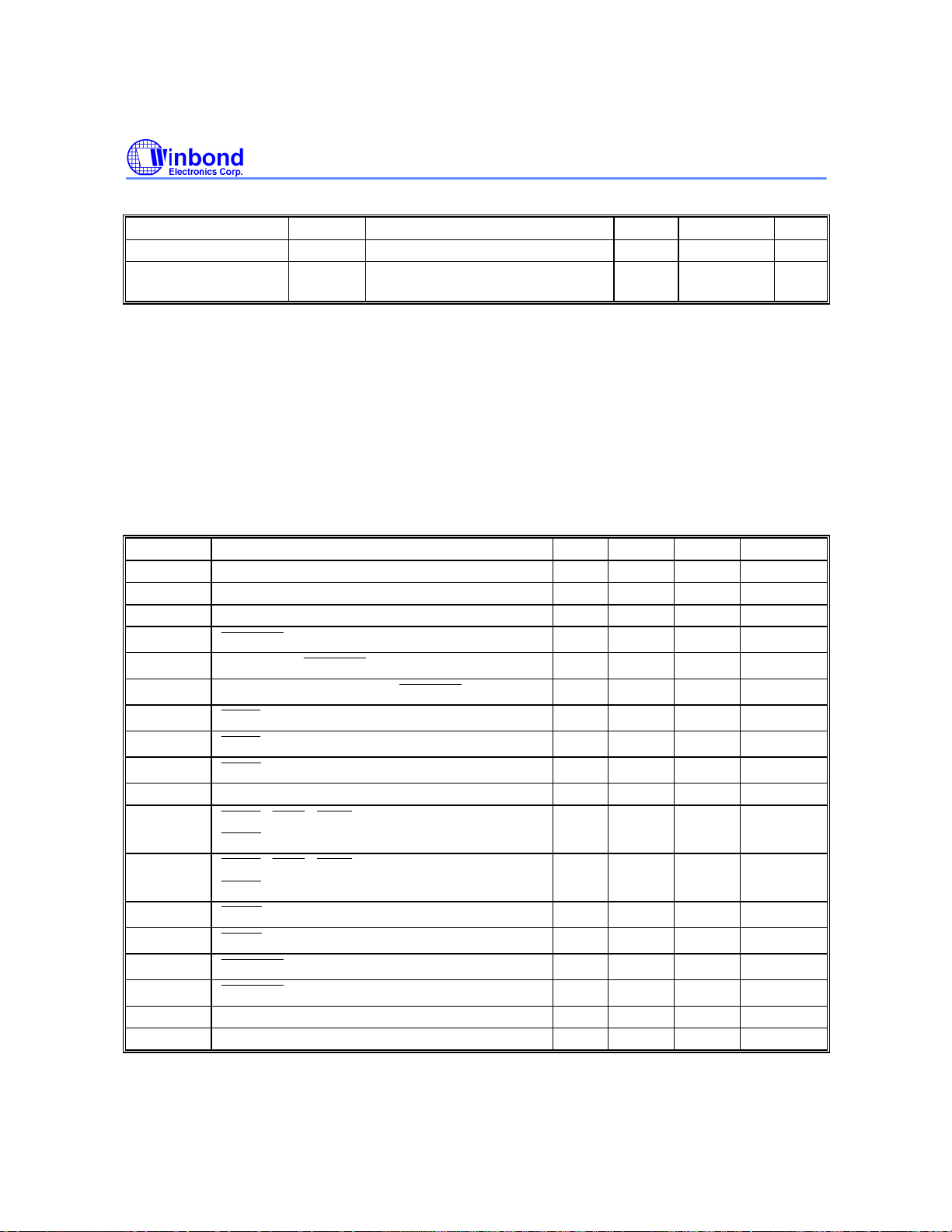
DC Characteristics, continued
PARAMETER SYM. CONDITIONS MIN. MAX. UNIT
Operating Current IDD FLCLK = 50 MHz - 25 mA
Standby Current ISTBY All input and I/O pins pulled high,
LCLK = VDD
AC CHARACTERISTICS
All AC timing is measured from the 0.8V and 2.0V on the source signal to the 0.8V and 2.0V level on
the signal under test.
AC specifications are given for the following testing conditions:
VDD = 5V ± 5%, Temp. = 0° C to 70° C
VL-Bus shared signal loading = 100 pF
VL-Bus non-shared signal loading = 33 pF
ISA Bus signal loading = 240 pF
IDE device interface loading = 30 pF
SYMBOL PARAMETER MIN. MAX. UNIT FIG.
t1 LCLK Period 20 - nS Fig. 1
t2 LCLK High Time 5 - nS Fig. 1
t3 LCLK Low Time 5 - nS Fig. 1
t4
t5
t6
t7
t8
t9
t10 VESA IO Read Host Data Drive Delay 5 16 nS Fig. 2, 4
t11
t12
t13
t14
t15
t16
t17 VESA IO Write Host Data Valid Delay - 20 nS Fig. 3
t18 VESA IO Write Host Data Hold Time 0 - nS Fig. 3, 5
POS Pin to
POS Pin Hold Time from
Pulse Width
Setup Time
to LCLK Setup Time
Hold Time from LCLK
Active Delay from Address
,
,
asserted at T2
,
,
asserted at T2
Active Delay from LCLK
Inactive Delay from LCLK
to LCLK Setup Time
Hold Time from LCLK
to LCLK Setup Time when
to LCLK Setup Time when
16 - LCLK Fig. 1
200 - nS Fig. 1
10 - nS Fig. 1
6 - nS Fig. 2
3 - nS Fig. 2
39 nS Fig. 2
5 - nS Fig. 2, 3
10 - nS Fig. 2, 3
5 16 nS Fig. 2, 3
6 18 nS Fig. 2, 3
6 - nS Fig. 2, 3
3 - nS Fig. 2, 3
- 800
µA
Publication Release Date: May 1995
- 33 - Revision A1
Page 34
W83759A
IDE0CS0
IDE1CS0
IDE0CS0
IDE1CS0
IDEIOR
IDEIOW
IDEIOR
IDEIOW
IDECS0
1, IDECS1
1
IDE0CS1
IDE1CS1
IDEIOR
XIOW
VGAOEL
VGAOEH
IDEIOR
XIOR
IDEIOR
XIOR
IDEIOW
XIOW
IDEIOW
XIOW
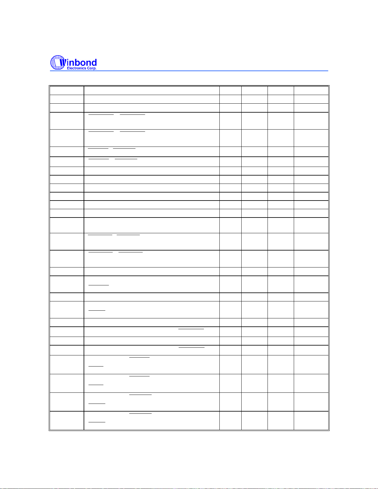
AC Characteristics, continued
SYMBOL PARAMETER MIN. MAX. UNIT FIG.
t19 IDEA[2:0] Valid Delay from Address Valid - 18 nS Fig. 4, 5
t20 IDEA[2:0] Invalid Delay from Address Change 5 18 nS Fig. 4, 5
t21
Address valid
t22
Address Change
t23
t24
t25 IDE Read IDD Data Hold Time from LCLK 0 - nS Fig. 4
t26 IDE Read IDD to HD Delay - 16 nS Fig. 4
t27 IDE Read HD Float Delay from LCLK 10 30 nS Fig. 4
t28 IDE Write IDD Drive Delay - 20 nS Fig. 5
t29 IDE Write IDD Float Delay 10 30 nS Fig. 5
t30 IDEA[2:0] Valid Delay from A2 SA[1:0] Valid - 20 nS Fig. 6, 7
t31 IDEA[2:0] Invalid Delay from A2 SA[1:0]
Change
t32
Valid
t33
Address Change
t34 ISA IDE Read IDD to SD Delay 8 18 nS Fig. 6
t35 ISA IDE Read IDD Data Hold Time from
,
,
,
,
,
Valid Delay from
Invalid Delay from
Active Delay from LCLK
Inactive Delay from LCLK
Valid Delay from Address
Invalid Delay from
- 18 nS Fig. 4, 5
5 18 nS Fig. 4, 5
- 22 nS Fig. 4, 5
- 24 nS Fig. 4, 5
5 20 nS Fig. 6, 7
- 17 nS Fig. 6, 7
4 17 nS Fig. 6, 7
5 - nS Fig. 6
t36 ISA IDE Write SD to IDD Delay 8 18 nS Fig. 7
t37 ISA IDE Wrtie SD Data Hold Time from
t38 VGA Read IDD to HD Delay - 16 nS Fig. 8
t39
t40 VGA Write HD to IDD Delay - 16 nS Fig. 9
t41
t42
t43
t44
t45
VGA Read HD Float Delay from
VGA Write HD Float Delay from
ISA IDD Read
ISA IDD Read
ISA IDE Write
ISA IDE Write
Active Delay from
Inactive Delay from
Active Delay from
Inactive Delay from
- 34 -
30 - nS Fig. 7
- 20 nS Fig. 8
- 20 nS Fig. 9
- 20 nS Fig. 6
- 20 nS Fig. 6
- 20 nS Fig. 7
- 20 nS Fig. 7
Page 35
W83759A
SYSRST
SYSRST
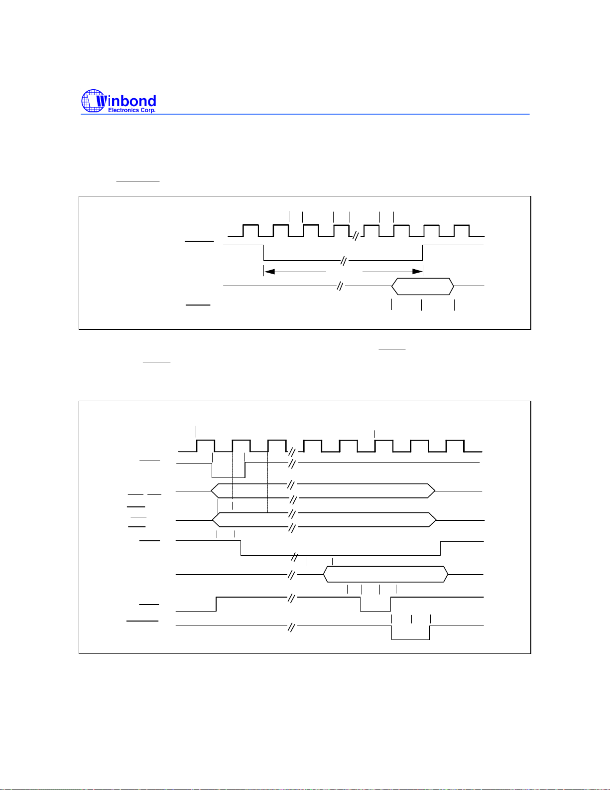
TIMING WAVEFORMS
All AC timing is measured from the 0.8V and 2.0V on the source signal to the 0.8V and 2.0V level on
the signal under test.
LCLK,
IDD[15:0], EMD1, EMD0
Note: ENIDE, TEST, SP1, MD1, MD0, PRDYEN, SRDYEN, IDD[15:0], EMD1, EMD0, DMASL are POS (Power-On Setting)
pins. When
, Timing
LCLK
SYSRST
ENIDE, TEST
SP1, MD1, MD0
PRDYEN, SRDYEN
DMASL
is low they are tri-stated as inputs.
t1 t2 t3
t4
t5 t6
Figure 1
VESA IO Read Timing
Local IDE Time
T1
LCLK
LADS
T2
t8
t7
HA[9:2],
BE2, BE0
HMIO = 0
HDC = 1
HWR = 0
LDEV
HD[31:0]
LRDY
RDYRTN
Note: Local IDE cycle time is determined by SP1, MD1, and MD0 or by SP1, EMD1 and EMD0 at power-on. After power-on the
driver can program the timing register to tune the timing.
t11
t12
t9
t10
t13
Figure 2
t14
t15
t16
Publication Release Date: May 1995
- 35 - Revision A1
Page 36
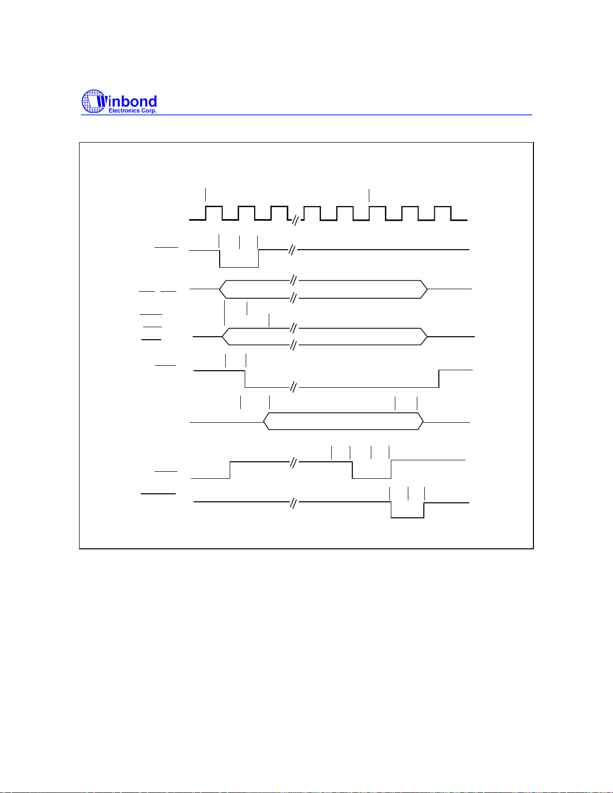
VESA IO Write Timing
LCLK
LADS
HA[9:2],
BE2, BE0
HMIO = 0
HDC = 1
HWR = 1
LDEV
W83759A
Local IDE Cycle Time
T1 T2
t7 t8
t11
t12
t9
HD[31:0]
LRDY
RDYRTN
t17
Figure 3
t13
t18
t14
t15 t16
- 36 -
Page 37
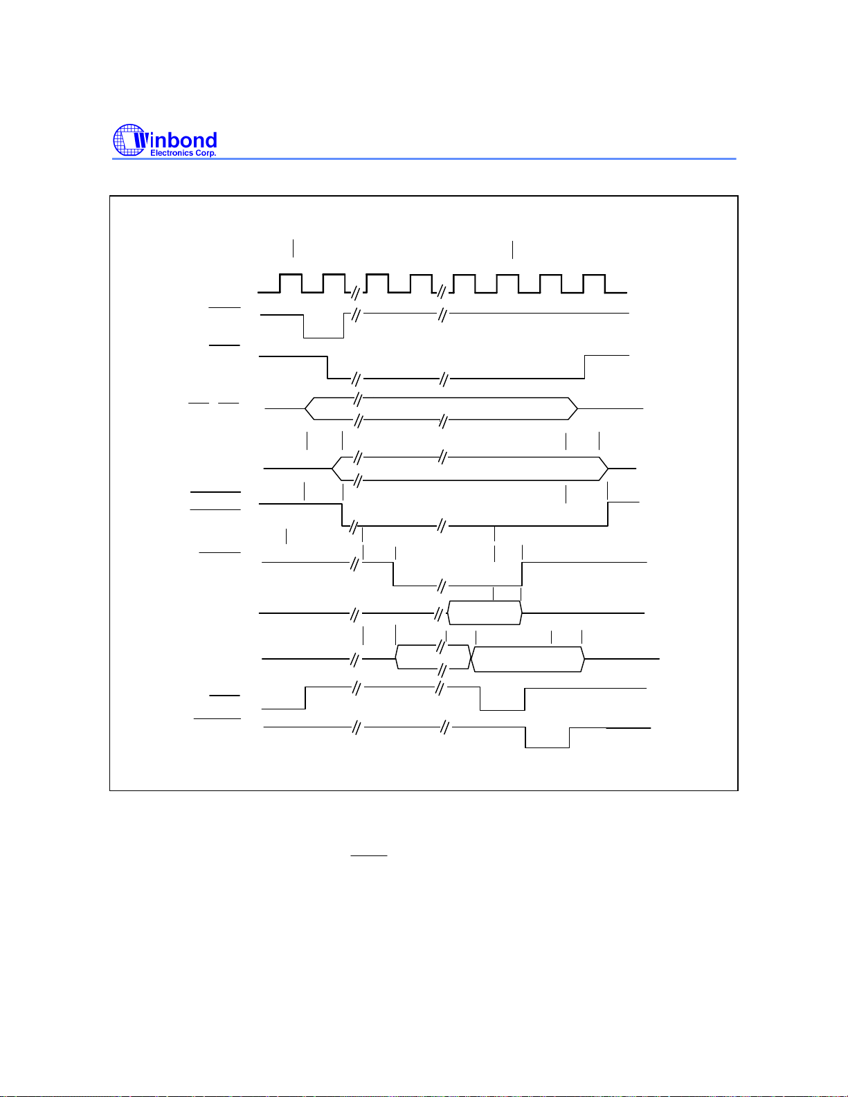
IDE IO Read Timing
LCLK
LADS
LDEV
HA[9:2],
BE2, BE0
T1
W83759A
Local IDE Cycle Time
T2
t19
t20
IEDA[2:0]
IDE0CS0
t21
t22
IDE1CS0
Recovery
Time
IDEIOR
Pulse Width
t23
t24
t25
IDD[15:0]
t10
t26 t27
HD[31:0]
LRDY
RDYRTN
Figure 4
Note: At power-on the recovery time and pulse width are determined by SP1, MD1, and MD0, or by SP1, EMD1 and EMD0 as
indicated in Table 7. and Table 8. After power-on the driver can program the timing register to tune the timing.
Example: When SP = 1 and MD1 = MD0 = 0, the IDEIOR pulse width is 10 LCLK and recovery time is 21 LCLK (cycle time
is 31 LCLK).
Publication Release Date: May 1995
- 37 - Revision A1
Page 38
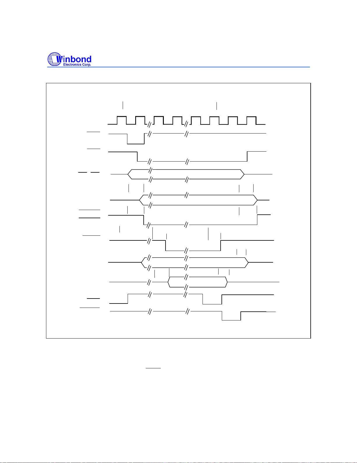
IDE IO Write Timing
IDEIOW
LCLK
LADS
LDEV
HA[9:2],
BE2, BE0
T1
W83759A
Local IDE Cycle Time
T2
IEDA[2:0]
IDE0CS0
IDE1CS0
IDEIOW
HD[31:0]
IDD[15:0]
LRDY
RDYRTN
t19
t21
Recovery
Time
Pulse Width
t23
t28
Figure 5
t20
t22
t24
t18
t29
Note: At power-on the recovery time and pulse width are determined by SP1, MD1, and MD0 or by SP1, EMD1, and EMD0 as
indicated in Table 7 and Table 8. After power-on the driver can program the timing register to tune the timing.
Example: When SP = 1 and MD1 = MD0 = 0, the
31 LCLK).
pulse width is 9 LCLK and recovery time is 22 LCLK (cycle time is
- 38 -
Page 39
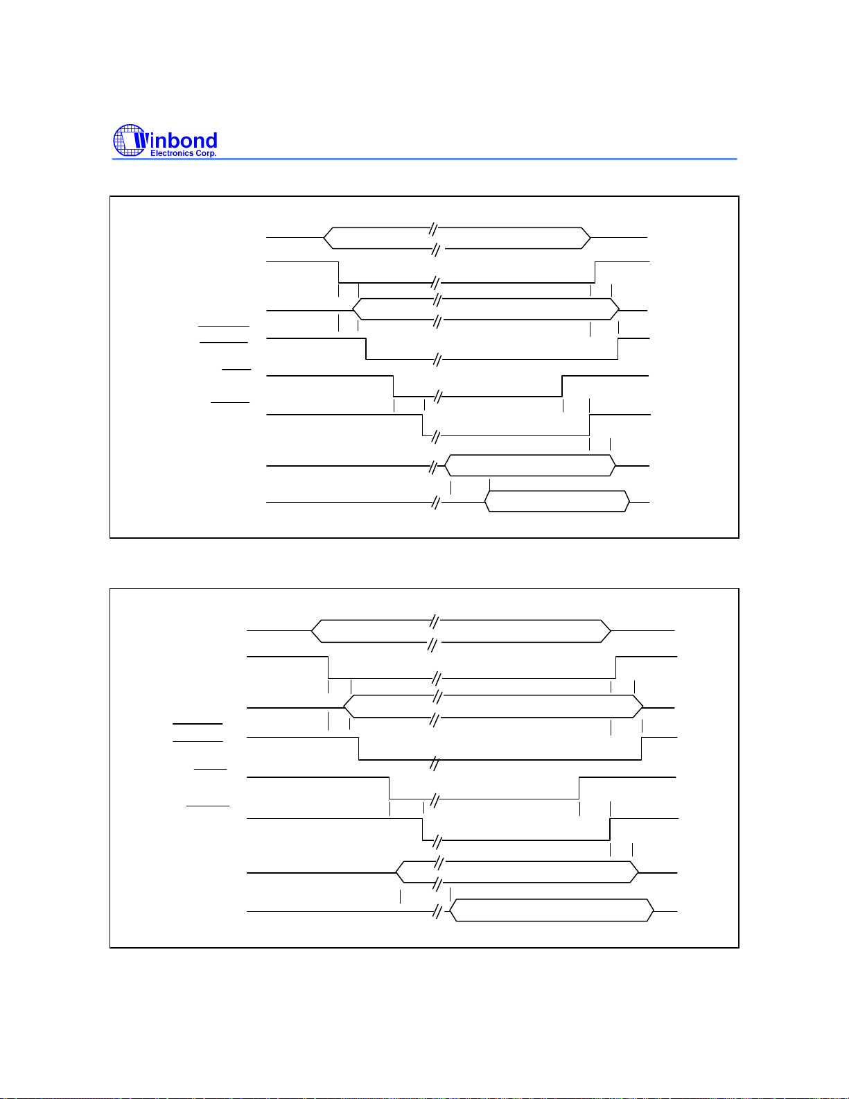
ISA IO Read Timing
SA1, SA0
AEN
W83759A
IDEA[1:0]
IDE0CS1,
IDE1CS1
XIOR
IDEIOR
IDD[7:0]
SD[7:0]
ISA IO Write Timing
SA1, SA0
AEN
IDEA[1:0]
IDE0CS1,
IDE1CS1
t30
t32
t30
t32
t42
Figure 6
t31
t33
t43
t35
t34
t31
t33
XIOW
IDEIOW
SD[7:0]
IDD[7:0]
t44
t36
Figure 7
t45
t37
Publication Release Date: May 1995
- 39 - Revision A1
Page 40
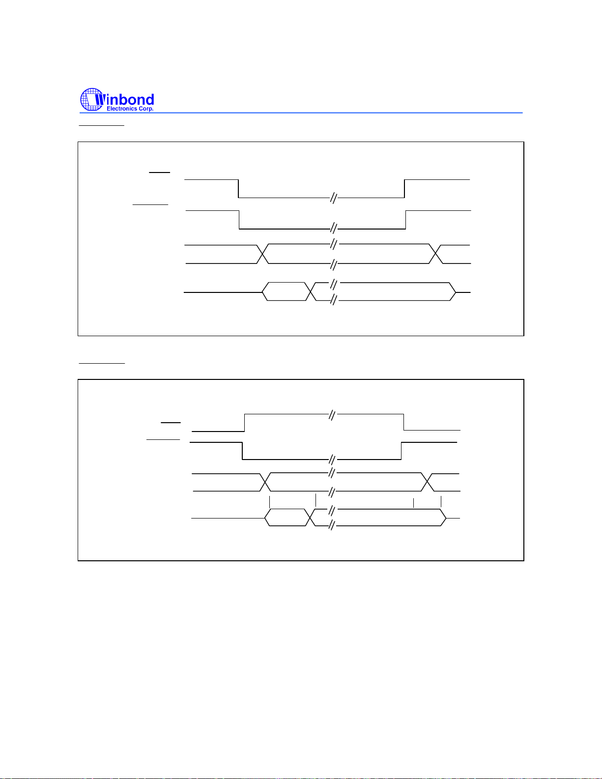
VGAOEL
Read Timing
VGAOEH
HWR
VGAOEL
IDD[15:0]
HD[15:0]
W83759A
Figure 8
Write Timing
HWR
VGAOEL
HD[31:16]
IDD[15:0]
t40
Figure 9
t41
- 40 -
Page 41
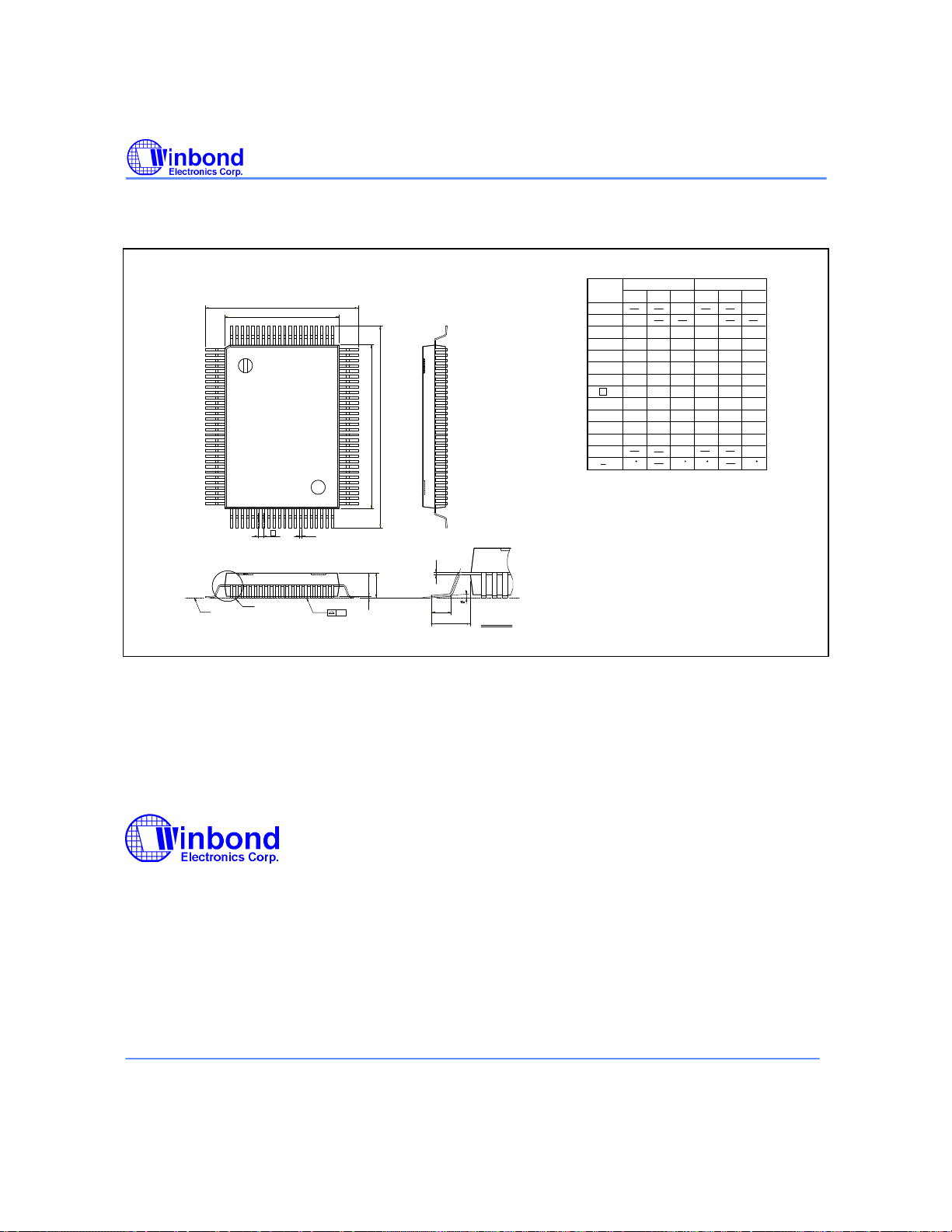
PACKAGE DIMENSION
100-pin QFP
W83759A
1
30
Seating Plane
H
D
e
See Detail F
Dimension in inches
D
81100
80
E
E H
51
5031
b
c
2
AA
1
A
y
L
L
1
Detail F
Symbol
A
A
A
b
c
D
E
e
H
H
L
L
y
0
Notes:
1. Dimension D & E do not include interlead
flash.
2. Dimension b does not include dambar
protrusion/intrusion.
3. Controlling dimension: Millimeters
4. General appearance spec. should be based on final
visual inspection spec.
Min.
0.004
1
0.107
2
0.010
0.004
0.546
0.782
0.020
0.728
D
0.964
E
0.039
0.087
1
Nom
0.112
0.012
0.006 0.15
0.551
0.787
0.026
0.740
0.976
0.047
0.094
Dimension in mm
Nom
Max. Max.
Min.
0.130
0.10
2.73
0.117
0.016
0.010
0.556
0.792
0.032
0.752
0.988
0.055
0.103
0.004
2.85
0.25
0.30
0.10
14.00
13.87
19.87
18.49
24.49 24.80 25.10
14.13
20.00
20.13
0.65
0.50 0.80
19.10
18.80
1.20
1.00
2.40
2.21
0120
3.30
2.97
0.40
0.25
1.40
2.62
0.10
12
Headquarters
No. 4, Creation Rd. III,
Science-Based Industrial Park,
Hsinchu, Taiwan
TEL: 886-3-5770066
FAX: 886-3-5792646
http://www.winbond.com.tw/
Voice & Fax-on-demand: 886-2-7197006
Winbond Electronics (H.K.) Ltd.
Rm. 803, World Trade Square, Tower II,
123 Hoi Bun Rd., Kwun Tong,
Kowloon, Hong Kong
TEL: 852-27516023
FAX: 852-27552064
Taipei Office
11F, No. 115, Sec. 3, Min-Sheng East Rd.,
Taipei, Taiwan
TEL: 886-2-7190505
FAX: 886-2-7197502
Note: All data and specifications are subject to change without notice.
Winbond Electronics North America Corp.
Winbond Memory Lab.
Winbond Microelectronics Corp.
Winbond Systems Lab.
2730 Orchard Parkway, San Jose,
CA 95134, U.S.A.
TEL: 1-408-9436666
FAX: 1-408-9436668
Publication Release Date: May 1995
- 41 - Revision A1
 Loading...