

Page 1

W83697SF
WINBOND I/O
Page 2

W83697SF Data Sheet Revision History
Pages Dates Version Version
on Web
Main Contents
1 n.a. 04/16/01 0.50 0.50 First published
2 111
04/27/01 0.51 0.51 Update the Top Marking
3
4
5
6
7
8
9
10
Please note that all data and specifications are subject to change without notice. All the
trade marks of products and companies mentioned in this data sheet belong to their
respective owners.
LIFE SUPPORT APPLICATIONS
These products are not designed for use in life support appliances, devices, or systems
where malfunction of these products can reasonably be expected to result in personal
injury. Winbond customers using or selling these products for use in such applications
do so at their own risk and agree to fully indemnify Winbond for any damages resulting
from such improper use or sales.
Page 3

W83697SF
PRELIMINARY
Publication Release Date: April 2001
- I - Revision 0.50
TABLE OF CONTENT
GENERAL DESCRIPTION .............................................................................................................. 1
PIN CONFIGURATION FOR 697SF................................................................................................ 6
1.0 PIN DESCRIPTION................................................................................................................ 7
1.1 LPC INTERFACE........................................................................................................................ 7
1.2 FDC INTERFACE........................................................................................................................ 9
1.3 MULTI-MODE PARALLEL PORT.....................................................................................................10
1.4 SERIAL PORT INTERFACE............................................................................................................15
1.5 INFRARED PORT ........................................................................................................................16
1.6 FRESH ROM INTERFACE.............................................................................................................16
1.7 GENERAL PURPOSE I/O PORT .....................................................................................................17
1.8 SMART CARD INTERFACE............................................................................................................17
1.9 PWM & GENERAL PURPOSE I/O PORT 8 ...................................................................................... 18
1.10 GAME PORT & MIDI PORT ........................................................................................................18
1.11 POWER PINS...................................................................................................................... 19
2.0 LPC (LOW PIN COUNT) INTERFACE...................................................................................... 20
3.0 FDC FUNCTIONAL DESCRIPTION.........................................................................................21
3.1 W83697SF FDC .....................................................................................................................21
3.1.1 AT interface.....................................................................................................................21
3.1.2 FIFO (Data) .....................................................................................................................21
3.1.3 Data Separator .................................................................................................................22
3.1.4 Write Precompensation.....................................................................................................22
3.1.5 Perpendicular Recording Mode...........................................................................................23
3.1.6 FDC Core ........................................................................................................................23
3.1.7 FDC Commands ...............................................................................................................23
3.2 REGISTER DESCRIPTIONS.............................................................................................................36
3.2.1 Status Register A (SA Register) (Read base address + 0)...................................................36
3.2.2 Status Register B (SB Register) (Read base address + 1)...................................................38
3.2.3 Digital Output Register (DO Register) (Write base address + 2) ............................................40
3.2.4. Tape Drive Register (TD Register) (Read base address + 3) ................................................40
3.2.5 Main Status Register (MS Register) (Read base address + 4)...............................................43
3.2.6 Data Rate Register (DR Register) (Write base address + 4) .................................................43
3.2.7 FIFO Register (R/W base address + 5).............................................................................. 45
3.2.8 Digital Input Register (DI Register) (Read base address + 7)................................................46
3.2.9 Configuration Control Register (CC Register) (Write base address + 7)..................................48
4.0 UART PORT ..........................................................................................................................49
Page 4

W83697SF
PRELIMINARY
Publication Release Date: April 2001
- II - Revision 0.51
4.1 UNIVERSAL ASYNCHRONOUS RECEIVER /TRANSMITTER (UART A, UART B)..........................................49
4.2 REGISTER ADDRESS ...................................................................................................................49
4.2.1 UART Control Register (UCR) (Read/Write).........................................................................49
4.2.2 UART Status Register (USR) (Read/Write) .........................................................................51
4.2.3 Handshake Control Register (HCR) (Read/Write) .................................................................52
4.2.4 Handshake Status Register (HSR) (Read/Write)..................................................................53
4.2.5 UART FIFO Control Register (SFR) (Write only) ..................................................................54
4.2.6 Interrupt Status Register (ISR) (Read only) .........................................................................55
4.2.7 Interrupt Control Register (ICR) (Read/Write).......................................................................57
4.2.8 Programmable Baud Generator (BLL/BHL) (Read/Write) ...................................................... 57
4.2.9 User-defined Register (UDR) (Read/Write)..........................................................................58
5.0 PARALLEL PORT.................................................................................................................59
5.1 PRINTER INTERFACE LOGIC ..........................................................................................................59
5.2 ENHANCED PARALLEL PORT (EPP).............................................................................................. 60
5.2.1 Data Swapper ...................................................................................................................62
5.2.2 Printer Status BSFfer .......................................................................................................62
5.2.3 Printer Control Latch and Printer Control Swapper................................................................62
5.2.4 EPP Address Port............................................................................................................63
5.2.5 EPP Data Port 0-3............................................................................................................64
5.2.6 Bit Map of Parallel Port and EPP Registers ........................................................................64
5.2.7 EPP Pin Descriptions .......................................................................................................66
5.2.8 EPP Operation.................................................................................................................66
5.3 EXTENDED CAPABILITIES PARALLEL (ECP) PORT............................................................................68
5.3.1 ECP Register and Mode Definitions....................................................................................68
5.3.2 Data and ecpAFifo Port .....................................................................................................69
5.3.3 Device Status Register (DSR)............................................................................................69
5.3.4 Device Control Register (DCR)...........................................................................................70
5.3.5 cFifo (Parallel Port Data FIFO) Mode = 010 ........................................................................71
5.3.6 ecpDFifo (ECP Data FIFO) Mode = 011.............................................................................. 71
5.3.7 tFifo (Test FIFO Mode) Mode = 110...................................................................................71
5.3.8 cnfgA (Configuration Register A) Mode = 111 ......................................................................71
5.3.9 cnfgB (Configuration Register B) Mode = 111 ......................................................................71
5.3.10 ecr (Extended Control Register) Mode = all........................................................................72
5.3.11 Bit Map of ECP Port Registers .........................................................................................73
5.3.12 ECP Pin Descriptions .....................................................................................................75
5.3.13 ECP Operation...............................................................................................................76
5.3.14 FIFO Operation .............................................................................................................. 76
5.3.15 DMA Transfers ...............................................................................................................77
5.3.16 Programmed I/O (NON- DMA) Mode..................................................................................77
5.4 EXTENSION FDD MODE (EXTFDD)...............................................................................................77
5.5 EXTENSION 2FDD MODE (EXT2FDD)...........................................................................................77
6.0 GENERAL PURPOSE I/O.......................................................................................................78
7.0 ACPI REGISTERS FEATURES ...............................................................................................82
Page 5

W83697SF
PRELIMINARY
Publication Release Date: April 2001
- III - Revision 0.51
8.0 PULSE WIDTH MODULATION (PWM)....................................................................................83
8.1 GENERAL DESCRIPTION...............................................................................................................83
8.2 LPC INTERFACE.......................................................................................................................83
8.3 REGISTERS ..........................................................................................................................84
8.3.1 Address Register (Port x5h)...............................................................................................84
8.3.2 Data Register (Port x6h) ....................................................................................................84
8.3.3 PWM 1 Pre-Scale Register -- Index 00h ..............................................................................85
8.3.4 PWM 1 Duty Cycle Select Register – Index 01h ..................................................................85
8.3.5 PWM 2 Pre-Scale Register -- Index 02h ..............................................................................86
8.3.6 PWM 2 Duty Cycle Select Register -- Index 03h ..................................................................86
8.3.7 PWM 0 Pre-Scale Register -- Index 10h ..............................................................................87
8.3.8 PWM 0 Duty Cycle Select Register – Index 11h..................................................................87
9.0 CONFIGURATION REGISTER................................................................................................88
9.1 PLUG AND PLAY C ONFIGURATION ................................................................................................88
9.2 COMPATIBLE PNP.....................................................................................................................88
9.2.1 Extended Function Registers.............................................................................................88
9.2.2 Extended Functions Enable Registers (EFERs) ..................................................................89
9.2.3 Extended Function Index Registers (EFIRs), Extended Function Data Registers(EFDRs)........89
9.3 CONFIGURATION SEQUENCE .........................................................................................................89
9.3.1 Enter the extended function mode ......................................................................................89
9.3.2 Configurate the configuration registers ................................................................................89
9.3.3 Exit the extended function mode........................................................................................89
9.3.4 Software programming example .........................................................................................90
9.4 CHIP (G LOBAL) CONTROL REGISTER .............................................................................................91
9.5 LOGICAL DEVICE 0 (FDC)...........................................................................................................99
9.6 LOGICAL DEVICE 1 (PARALLEL PORT)......................................................................................... 103
9.7 LOGICAL DEVICE 2 (UART A)....................................................................................................104
9.8 LOGICAL DEVICE 3 (UART B)....................................................................................................105
9.9 LOGICAL DEVICE 7 (GAME PORT AND GPIO PORT 1).....................................................................107
9.10 LOGICAL DEVICE 8 (MIDI PORT AND GPIO PORT 5).....................................................................108
9.11 LOGICAL DEVICE 9 (GPIO PORT 2 ~ GPIO PORT 4 )...................................................................110
9.12 LOGICAL DEVICE A (ACPI)......................................................................................................111
9.13 LOGICAL DEVICE B (PWM).....................................................................................................117
9.14 LOGICAL DEVICE C (SMART CARD)........................................................................................ 117
9.15 LOGICAL DEVICE D (URC & GPIO PORT 6 )..............................................................................118
9.16 LOGICAL DEVICE E (URD & GPIO PORT 7 ).............................................................................. 119
9.17 LOGICAL DEVICE F (GPIO PORT 8) ..........................................................................................120
10.0 ORDERING INSTRUCTION................................................................................................. 122
11.0 HOW TO READ THE TOP MARKING ..................................................................................122
12.0 PACKAGE DIMENS IONS ....................................................................................................123
Page 6

W83697SF
PRELIMINARY
Publication Release Date: April 2001
- 1 - Revision 0.50
GENERAL DESCRIPTION
The W83697SF is evolving product from Winbond's most popular I/O family. They feature a whole new
interface, namely LPC (Low Pin Count) interface, which will be supported in the new generation chip-
set. This interface as its name suggests is to provide an economical implementation of I/O's interface
with lower pin count and still maintains equivalent performance as its ISA interface counterpart.
Approximately 40 pin counts are saved in LPC I/O comparing to ISA implementation. With this
additional freedom, we can implement more devices on a single chip as demonstrated in W83697SF's
integration of Game Port and MIDI Port. It is fully transparent in terms of software which means no BIOS
or device driver update is needed except chip-specific configuration.
As Smart Card application is gaining more and more attention, W83697SF also implements a smart
card reader interface featuring Smart wake -up function. This smart card reader interface fully meets the
ISO7816 and PC/SC (Personal Computer/Smart Card Workgroup) standards. W83697SF provides a
minimum extern al components and lowest cost solution for smart card applications.
The disk drive adapter functions of W83697SF include a floppy disk drive controller compatible with the
industry standard 82077/ 765, data separator, write pre-compensation circuit, decode logic, data rate
selection, clock generator, drive interface control logic, and interrupt and DMA logic. The wide range of
functions integrated onto the W83697SF greatly reduces the number of components required for
interfacing with floppy disk drives. The W83697SF supports four 360K, 720K, 1.2M, 1.44M, or 2.88M
disk drives and data tranSFer rates of 250 Kb/s, 300 Kb/s, 500 Kb/s,1 Mb/s, and 2 Mb/s.
The W83697SF provides two high-speed serial communication ports (UARTs), one of which supports
serial Infrared communication. Each UART includes a 16-byte send/receive FIFO, a programmable baud
rate generator, complete modem control capability, and a processor interrupt system. Both UARTs
provide legacy speed with baud rate up to 115.2k bps and also advanced speed with baud rates of 230k,
460k, or 921k bps which support higher speed modems. In addition, the W83697SF provides IR
functions: IrDA 1.0 (SIR for 1.152K bps) and TV remote IR (Consumer IR, supporting NEC, RC-5,
extended RC-5, and RECS -80 protocols).
The W83697SF supports one PC-compatible printer port (SPP), Bi-directional Printer port (BPP) and
also Enhanced Parallel Port (EPP) and Extended Capabilities Port (ECP). Through the printer port
interface pins, also available are: Extension FDD Mode and Ext ension 2FDD Mode allowing one or two
external floppy disk drives to be connected.
The configuration registers support mode selection, function enable/disable, and power down function
selection. Furthermore, the configurable PnP features are compatible with the plug-and -play feature
demand of Windows 95/98TM, which makes system resource allocation more efficient than ever.
The W83697SF provides a set of flexible I/O control functions to the system designer through a set of
General Purpose I/O ports. These GPIO ports may serve as simple I/O or may be individually configured
Page 7

W83697SF
PRELIMINARY
Publication Release Date: April 2001
- 2 - Revision 0.51
to provide a predefined alternate function. General Purpose Port 1 is designed to be functional even in
power down mode (VCC is off).
The W83697SF is made to fully comply with Microsoft PC98 and PC99 Hardware Design Guide,
and meet the requirements of ACPI.
The W83697SF contains a game port and a MIDI port. The game port is designed to support 2 joysticks
and can be applied to all standard PC game control devices, They are very important for a entertainment
or consumer computer.
The W83697SF provides Flash ROM interface . That can support up to 4M legacy flash ROM.
Moreover, W83697SF support 3 sets PWM Fan Speed Control, which are very important for a high-
end computer system to work stably and properly.
Page 8

W83697SF
PRELIMINARY
Publication Release Date: April 2001
- 3 - Revision 0.51
FEATURES
General
• Meet LPC Spec. 1.01
• Support LDRQ#(LPC DMA), SERIRQ (serial IRQ)
• Include all the features of Winbond I/O W83877TF
• Integrate Smart Card functions
• Compliant with Microsoft PC98/PC99 Hardware Design Guide
• Support DPM (Device Power Management), ACPI
• Programmable configuration settings
• Single 24 or 48 MHz clock input
FDC
• Compatible with IBM PC AT disk drive systems
• Variable write pre- compensation with track selectable capability
• Support vertical recording format
• DMA enable logic
• 16 -byte data FIFOs
• Support floppy disk drives and tape drives
• Detects all overrun and underrun conditions
• Built-in address mark detection circuit to simplify the read electronics
• FDD anti -virus functions with software write protect and FDD write enable signal (write data signal
was forced to be inactive)
• Support up to four 3.5 -inch or 5.25-inch floppy disk drives
• Completely compatible with industry standard 82077
• 360K/720K/1.2M/1.44M/2.88M format; 250K, 300K, 500K, 1M, 2M bps data transfer rate
• Support 3-mode FDD, and its Win95/98 driver
UART
• Two high-speed 16550 compatible UARTs with 16-byte send/receive FIFOs
• MIDI compatible
• Fully programmable serial -interface characteristics:
--- 5, 6, 7 or 8-bit characters
--- Even, odd or no parity bit generation/detection
--- 1, 1.5 or 2 stop bits generation
Page 9

W83697SF
PRELIMINARY
Publication Release Date: April 2001
- 4 - Revision 0.51
• Internal diagnostic capabilities:
--- Loop-back controls for communications link fault isolation
--- Break, parity, overrun, framing error simulation
• Programmable baud generator allows division of 1.8461 MHz and 24 MHz by 1 to (216-1)
• Maximum baud rate up to 921k bps for 14.769 MHz and 1.5M bps for 24 MHz
Infrared
• Support IrDA version 1.0 SIR protocol with maximum baud rate up to 115.2K bps
• Support SHARP ASK-IR protocol with maximum baud rate up to 57,600 bps
• Support Consumer IR with Wake-Up function.
Parallel Port
• Compatible with IBM parallel port
• Support PS/2 compatible bi-directional parallel port
• Support Enhanced Parallel Port (EPP) − Compatible with IEEE 1284 specification
• Support Extended Capabilities Port (ECP) − Compatible with IEEE 1284 specification
• Extension FDD mode supports disk drive B; and Extension 2FDD mode supports disk drives A and
B through parallel port
• Enhanced printer port back -drive current protection
Page 10

W83697SF
PRELIMINARY
Publication Release Date: April 2001
- 5 - Revision 0.51
Game Port
• Support two separate Joysticks
• Support every Joystick two axes (X,Y) and two buttons (S1,S2) controllers
MIDI Port
• The baud rate is 31.25 Kbaud
• 16 -byte input FIFO
• 16 -byte output FIFO
Flash ROM Interface
• Support up to 4M flash ROM
General Purpose I/O Ports
• 60 programmable general purpose I/O ports
• General purpose I/O ports can serve as simple I/O ports, watch dog timer output, power LED
output, infrared I/O pins, suspend LED output, Beep output
• Functional in power down mode
Smart Card Reader Interface
• ISO7816 protocol compliant
• PC/SC T=0, T=1 compliant
Fan Speed Control
• 3 Sets PWM Fan Speed Control
Package
• 128 -pin PQFP
Page 11
W83697SF
PRELIMINARY
Publication Release Date: April 2001
- 6 - Revision 0.51
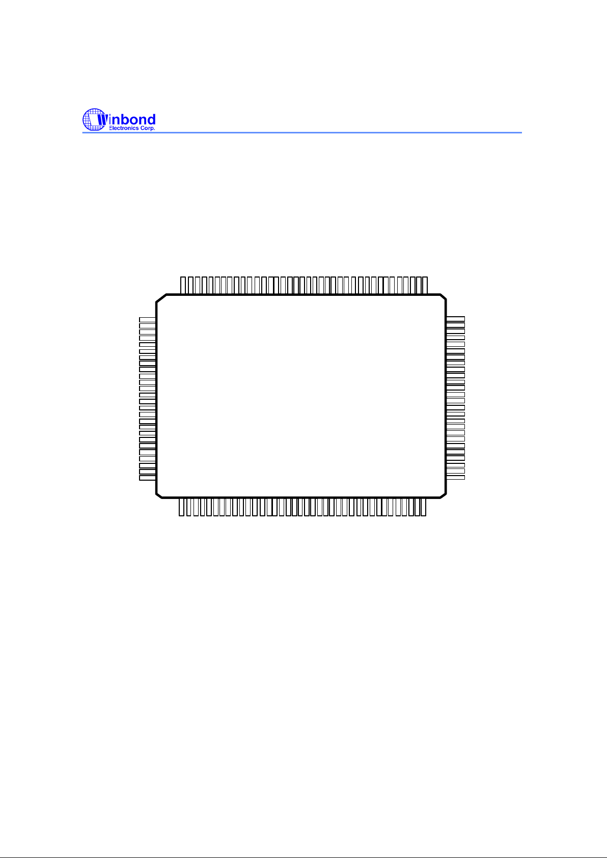
PIN CONFIGURATION FOR 697SF
64
63
62
61
60
59
58
57
56
55
54
53
52
51
50
49
48
47
46
45
44
43
42
41
40
39
103
104
105
106
107
108
109
110
111
112
113
114
115
116
117
118
119
120
121
122
123
124
125
126
127
128
2 1 0
1
0101099
989
7
969594939
29190898887
868
5
8483828180797
8777675
747
3
727
1706968676665
1 2 3 4 5 6 7 8 91011121314151617181920212223242526272829303132333435363738
DRVDEN0
INDEX#
GND
MOA#
DSB#
DSA#
MOB#
STEP#
DIR#
WD#
WE#
VCC
TRAK0#
WP#
RDATA#
HEAD#
DSKCHG#
CLKIN#
PME#
SLIN#
PCICLK
LDRQ#
SERIRQ
LAD3
LAD2
LAD1
VCC3
LAD0
LFRAME#
LRESET#
SLCT
PE
BUSY
ACK#
PD4
PD5
PD7
PD6
RIB#
DCDB#
SOUTB
SINB
GND
DTRB#
RTSB#
RIA#
DCDA#
CTSB#
SOUTA
SINA
DTRA#
RTSA#
DSRA#
CTSA#
VCC
STB#
AFD#
DSRB#
INIT#
PD0
PD1
PD2
PD3
IRTX
XA18/GP57
VCC
XA17/GP56
XA16/GP55
MEMR#/GP53
MEMW#/GP52
GP64
ROMCS#/GP54
GP65
GP66
GP67
GND
GP63
GP62
GP61
GP60
SCPSNT/GP77
SCIO/GP76
SCCLK/GP75
SCRST/GP74
GP73
SCC8/GP72
SCPWR/GP71
SCC4/GP70
PWM1/GP82
PWM2/PLED/GP83
PWM0/GP81
WDTO/GP80
MSI/GP51
MSO/GP50
GPAS2/GP17
GPBS2/GP16
GPAY/GP15
GPBY/GP14
GPBX/GP13
GPAX/GP12
GPBS1/GP11
GPAS1/GP10
IRRX
ERR#
XA15/GP47
XA14/GP46
XA13/GP45
XA12/GP44
XA11/GP43
XA10/GP42
XA9/GP41
XA8/GP40
XA7/GP37
XA6/GP36
XA5/GP35
XA4/GP34
XA3/GP33
XA2/GP32
XA0/GP30
XA1/GP31
XD7/GP27
XD6/GP26
XD5/GP25
XD4/GP24
XD3/GP23
XD2/GP22
XD1/GP21
XD0/GP20
W83697SF
64
63
62
61
60
59
58
57
56
55
54
53
52
51
50
49
48
47
46
45
44
43
42
41
40
64
63
62
61
60
59
58
57
56
55
54
53
52
51
50
49
48
47
46
45
44
43
42
41
40
39
103
104
105
106
107
108
109
110
111
112
113
114
115
116
117
118
119
120
121
122
123
124
125
126
127
128
2 1 0
1
0101099
989
7
969594939
29190898887
868
5
8483828180797
8777675
747
3
727
1706968676665
1 2 3 4 5 6 7 8 910101111121213131414151516161717181819192020212122222323242425252626272728282929303031313232333334343535363637373838
DRVDEN0
INDEX#
GND
MOA#
DSB#
DSA#
MOB#
STEP#
DIR#
WD#
WE#
VCC
TRAK0#
WP#
RDATA#
HEAD#
DSKCHG#
CLKIN#
PME#
SLIN#
PCICLK
LDRQ#
SERIRQ
LAD3
LAD2
LAD1
VCC3
LAD0
LFRAME#
LRESET#
SLCT
PE
BUSY
ACK#
PD4
PD5
PD7
PD6
RIB#
DCDB#
SOUTB
SINB
GND
DTRB#
RTSB#
RIA#
DCDA#
CTSB#
SOUTA
SINA
DTRA#
RTSA#
DSRA#
CTSA#
VCC
STB#
AFD#
DSRB#
INIT#
PD0
PD1
PD2
PD3
IRTX
XA18/GP57
VCC
XA17/GP56
XA16/GP55
MEMR#/GP53
MEMW#/GP52
GP64
ROMCS#/GP54
GP65
GP66
GP67
GND
GP63
GP62
GP61
GP60
SCPSNT/GP77
SCIO/GP76
SCCLK/GP75
SCRST/GP74
GP73
SCC8/GP72
SCPWR/GP71
SCC4/GP70
PWM1/GP82
PWM2/PLED/GP83
PWM0/GP81
WDTO/GP80
MSI/GP51
MSO/GP50
GPAS2/GP17
GPBS2/GP16
GPAY/GP15
GPBY/GP14
GPBX/GP13
GPAX/GP12
GPBS1/GP11
GPAS1/GP10
IRRX
ERR#
XA15/GP47
XA14/GP46
XA13/GP45
XA12/GP44
XA11/GP43
XA10/GP42
XA9/GP41
XA8/GP40
XA7/GP37
XA6/GP36
XA5/GP35
XA4/GP34
XA3/GP33
XA2/GP32
XA0/GP30
XA1/GP31
XD7/GP27
XD6/GP26
XD5/GP25
XD4/GP24
XD3/GP23
XD2/GP22
XD1/GP21
XD0/GP20
W83697SF
Page 12
W83697SF
PRELIMINARY
Publication Release Date: April 2001
- 7 - Revision 0.51
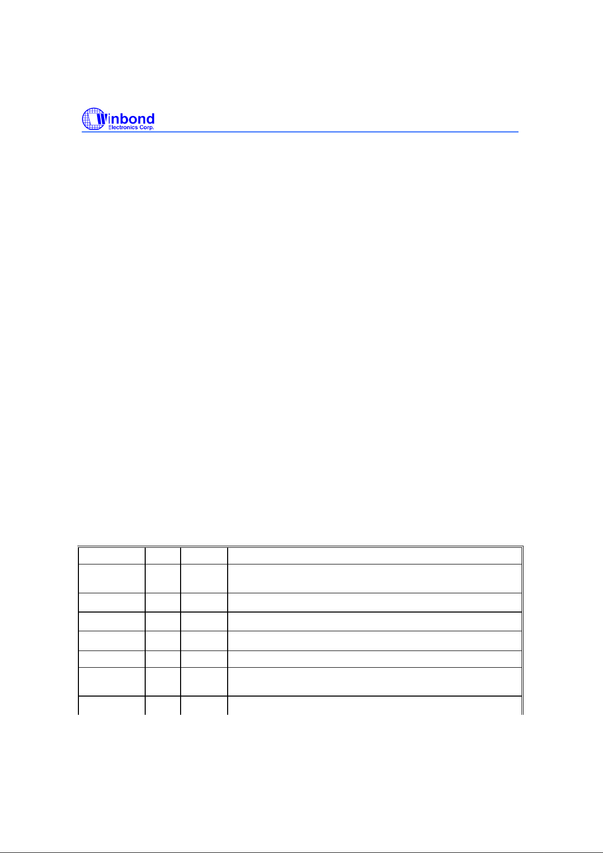
1.0 PIN DESCRIPTION
Note: Please refer to Section 13.2 DC CHARACTERISTICS for details.
I/O8t - TTL level bi-directional pin with 8 mA source-sink capability
I/O
16t
- TTL level bi-directional pin with 16 mA source-sink capability
I/O12ts - TTL level output pin with 12 mA sou rce-sink capability and Schmitt-trigger input pin
I/O
16ts
- TTL level output pin with 16 mA source -sink capability and Schmitt-trigger input pin
I/O
24cs
- TTL level output pin with 24 mA source-sink capability and CMOS level Schmitt-trigger input pin
I/OD
16t
- TTL level open-drain output pin with 16 mA source-sink capability and input pin
I/OD
24cs
- TTL level open-drain output pin with 24 mA source-sink capability and CMOS level Schmitt-trigger input pin
I/O
24tp3
- 3.3V TTL level bi-directional pin with 24 mA source -sink capability
O16 - Output pin with 16 mA source -sink capability
O24 - Output pin with 24 mA source -sink capability
OD8 - Open-drain output pin with 8 mA sink capability
OD16 - Open-drain output pin with 16 mA sink capability
OD20 - Open-drain output pin with 20 mA sink capability
OD24 - Open-drain output pin with 24 mA sink capability
O
24p3
- 3.3V output pin with 24 mA source-sink capability
INt - TTL level input pin
INts - TTL level Schmitt -trigger input pin
INcs - CMOS level Schmitt-trigger input pin
IN
tsp3
- 3.3V TTL level Schmitt-trigger input pin
1.1 LPC Interface
SYMBOL PIN I/O FUNCTION
CLKIN 17 INt System clock input. According to the input frequency 24MHz or
48MHz, it is selectable through register. Default is 24MHz input.
PME#
98 OD16 Generated PME event.
PCICLK 19 IN
tsp3
PCI clock input.
LDRQ# 20 O
24p3
Encoded DMA Request signal.
SERIRQ 21 I/O
24tp3
Serial IRQ input/Output.
LAD[3:0] 23-26 I/O
24tp3
These signal lines communicate address, control, and data
information over the LPC bus between a host and a peripheral.
LFRAME#
27 IN
tsp3
Indicates start of a new cycle or termination of a broken cycle.
Page 13

W83697SF
PRELIMINARY
Publication Release Date: April 2001
- 8 - Revision 0.51
LRESET#
28 IN
tsp3
Reset signal. It can connect to PCIRST# signal on the host.
Page 14
W83697SF
PRELIMINARY
Publication Release Date: April 2001
- 9 - Revision 0.51
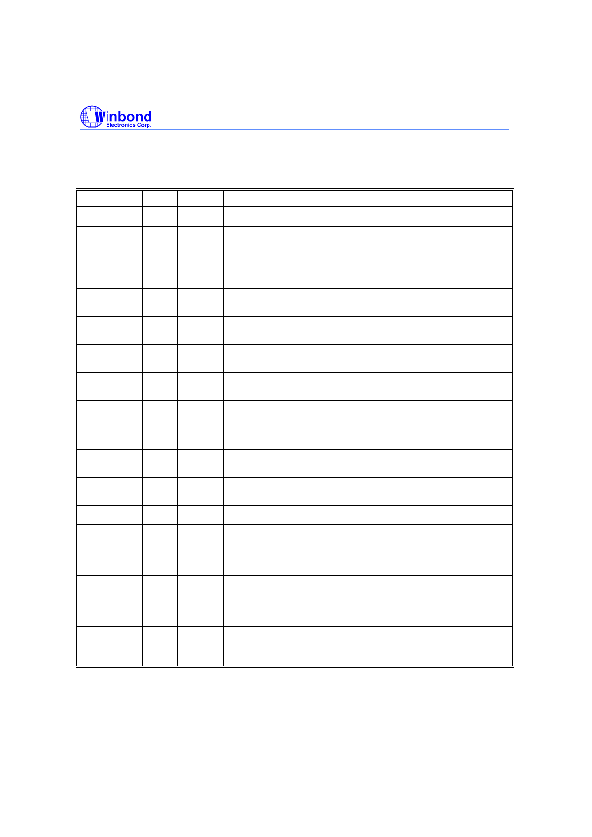
1.2 FDC Interface
SYMBOL PIN I/O FUNCTI ON
DRVDEN0 1 OD24 Drive Density Select bit 0.
INDEX#
2 INcs This Schmitt- triggered input from the disk drive is active low when
the head is positioned over the beginning of a track marked by an
index hole. This input pin is pulled up internally by a 1 KΩ
resistor. The resistor can be disabled by bit 7 of L0-CRF0
(FIPURDWN).
MOA#
3 OD24 Motor A On. When set to 0, this pin enables disk drive 0. This is
an open drain output.
DSB#
4 OD24 Drive Select B. When set to 0, this pin enables disk drive B. This
is an open drain output.
DSA#
6 OD24 Drive Select A. When set to 0, this pin enables disk drive A. This
is an open drain output.
MOB#
7 OD24 Motor B On. When set to 0, this pin enables disk drive 1. This is
an open drain output.
DIR#
8 OD24 Dire ction of the head step motor. An open drain output.
Logic 1 = outward motion
Logic 0 = inward motion
STEP#
9 OD24 Step output pulses. This active low open drain output produces a
pulse to move the head to another track.
WD#
10 OD
24
Write data. This logic low open drain writes pre-compensation
serial data to the selected FDD. An open drain output.
WE#
11 OD24 Write enable. An open drain output.
TRAK0#
12 INcs Track 0. This Schmitt-triggered input from the disk drive is active
low when the head is positioned over the outermost track. This
input pin is pulled up internally by a 1 KΩ resistor. The resistor
can be disabled by bit 7 of L0- CRF0 (FIPURDWN).
WP#
13 INcs Write protected. This active low Schmitt input from the disk drive
indicates that the diskette is write-protected. This input pin is
pulled up internally by a 1 KΩ res istor. The resistor can be
disabled by bit 7 of L0-CRF0 (FIPURDWN).
RDATA#
14 INcs The read data input signal from the FDD. This input pin is pulled
up internally by a 1 KΩ resistor. The resistor can be disabled by
bit 7 of L0-CRF0 (FIPURDWN).
Page 15

W83697SF
PRELIMINARY
Publication Release Date: April 2001
- 10 - Revision 0.51
1.2 FDC Interface, continued
SYMBOL PIN I/O FUNCTION
HEAD#
15 OD24 Head select. This open drain output determines which disk drive
head is active.
Logic 1 = side 0
Logic 0 = side 1
DSKCHG#
16 INcs Diskette change. This signal is active low at power on and
wh enever the diskette is removed. This input pin is pulled up
internally by a 1 KΩ resistor. The resistor can be disabled by bit 7
of L0 -CRF0 (FIPURDWN).
1.3 Multi-Mode Parallel Port
The following pins have alternate functions, which are controlled by CR28 and L3-CRF0.
SYMBOL PIN I/O FUNCTION
SLCT 29 INt
PRINTER MODE:
An active high input on this pin indicates that the printer is
selected. This pin is pulled high internally. Refer to the
description of the parallel port for definition of this pin in ECP and
EPP mode.
OD12
EXTENSION FDD MODE: WE2#
This pin is for Extension FDD B; its function is the same as the
WE#
pin of FDC.
OD12
EXTENSION 2FDD MODE: WE2#
This pin is for Extension FDD A and B; its function is the same as
the
WE#
pin of FDC.
PE
30 INt
PRINTER MODE:
An active high input on this pin indicates that the printer has
detected the end of the paper. This pin is pulled high internally.
Refer to the description of the parallel port for the definition of this
pin in ECP and EPP mode.
OD12
EXTENSION FDD MODE: WD2#
This pin is for Extension FDD B; its fu nction is the same as the
WD#
pin of FDC.
OD
12
EXTENSION 2FDD MODE: WD2#
This pin is for Extension FDD A and B; its function is the same as
the
WD#
pin of FDC.
Page 16

W83697SF
PRELIMINARY
Publication Release Date: April 2001
- 11 - Revision 0.51
1.3 Multi-Mode Parallel Port, continued
SYMBOL PIN I/O FUNCTION
BUSY 31 INt
PRINTER MODE:
An active high input indicates that the printer is not ready to
receive data. This pin is pulled high internally. Refer to the
description of the parallel port for definition of this pin in ECP and
EPP mode.
OD12
EXTENSION FDD MODE: MOB2#
This pin is for Extension FDD B; its function is the same as the
MOB# pin of FDC.
OD
12
EXTENSION 2FDD MODE: MOB2#
This pin is for Extension FDD A and B; its function is the same as
the MOB# pin of FDC.
ACK# 32 INt
OD12
OD
12
PRINTER MODE: ACK#
An active low input on this pin indicates that the printer has
received data and is ready to accept more data. This pin is pulled
high internally. Refer to the description of the parallel port for the
definition of this pin in ECP and EPP mode.
EXTENSION FDD MODE: DSB2#
This pin is for the Extension FDD B; its functions is the same as
the DSB# pin of FDC.
EXTENSION 2FDD MODE: DSB2#
This pin is for Extension FDD A and B; its function is the same as
the DSB# pin of FDC.
ERR#
33
INt
OD12
OD12
PRINTER MODE: ERR#
An active low input on this pin indicates that the printer has
encountered an error condition. This pin is pulled high internally.
Refer to the description of the parallel port for the definition of this
pin in ECP and EPP mode.
EXTENSION FDD MODE: HEAD2#
This pin is for Extension FDD B; its function is the same as the
HEAD#pin of FDC.
EXTENSION 2FDD MODE: HEAD2#
This pin is for Extension FDD A and B; its function is the same as
the HEAD# pin of FDC.
Page 17

W83697SF
PRELIMINARY
Publication Release Date: April 2001
- 12 - Revision 0.51
1.3 Multi-Mode Parallel Port, continued
SYMBOL PIN I/O FUNCTION
SLIN# 34 OD12
OD12
OD12
PRINTER MODE: SLIN#
Output line for detection of printer selection. This pin is pulled high
internally. Refer to the description of the parallel port for the
definition of this pin in ECP and EPP mode.
EXTENSION FDD MODE: STEP2#
This pin is for Extension FDD B; its function is the same as the
STEP# pin of FDC.
EXTENSION 2FDD MODE: STEP2#
This pin is for Extension FDD A and B; its function is the same as
the STEP# pin of FDC.
INIT#
43 OD12
OD12
OD12
PRINTER MODE: INIT#
Output line for the printer initialization. This pin is pulled high
internally. Refer to the description of the parallel port for the
definition of this pin in ECP and EPP mode.
EXTENSION FDD MODE: DIR2#
This pin is for Extension FDD B; its function is the same as the
DIR# pin of FDC.
EXTENSION 2FDD MODE: DIR2#
This pin is for Extension FDD A and B; its function is the same as
the DIR# pin of FDC.
AFD# 44 OD12
OD
12
OD12
PRINTER MODE: AFD#
An active low output from this pin causes the printer to auto feed a
line after a line is printed. This pin is pulled high internally. Refer to
the description of the parallel port for the definition of this pin in
ECP and EPP mode.
EXTENSION FDD MODE: DRVDEN0
This pin is for Extension FDD B; its function is the same as the
DRVDEN0 pin of FDC.
EXTENSION 2FDD MODE: DRVDEN0
This pin is for Extension FDD A and B; its function is the same as
the DRVDEN0 pin of FDC.
Page 18

W83697SF
PRELIMINARY
Publication Release Date: April 2001
- 13 - Revision 0.51
1.3 Multi-Mode Parallel Port, continued
SYMBOL PIN I/O FUNCTION
STB# 46 OD12 PRINTER MODE: STB#
An active low output is used to latch the parallel data into the
printer. This pin is pulled high internally. Refer to the description of
the parallel port for the definition of this pin in ECP and EPP mode.
- EXTENSION FDD MODE: This pin is a tri-state output.
- EXTENSION 2FDD MODE: This pin is a tri-state output.
PD0
42 I/O
12t
PRINTER MODE: PD0
Parallel port data bus bit 0. Refer to the description of the parallel
port for the definition of this pin in ECP and EPP mode.
INt
EXTENSION FDD MODE: INDEX2#
This pin is for Extension FDD B; its function is the same as the
INDEX# pin of FDC. It is pulled high internally.
INt EXTENSION 2FDD MODE: INDEX2#
This pin is for Extension FDD A and B; its function is the same as
the INDEX# pin of FDC. It is pulled high internally.
PD1
41 I/O
12t
INt
INt
PRINTER MODE: PD1
Parallel port data bus bit 1. Refer to the description of the parallel
port for the definition of this pin in ECP and EPP mode.
EXTENSION FDD MODE: TRAK02#
This pin is for Extension FDD B; its function is the same as the
TRAK0# pin of FDC. It is pulled high internally.
EXTENSION. 2FDD MODE: TRAK02#
This pin is for Extension FDD A and B; its function is the same as
the TRAK0# pin of FDC. It is pulled high internally.
PD2
40 I/O
12t
INt
IN
t
PRINTER MODE: PD2
Parallel port data bus bit 2. Refer to the description of the parallel
port for the definition of this pin in ECP and EPP mode.
EXTENSION FDD MODE: WP2#
This pin is for Extension FDD B; its function is the same as the
WP# pin of FDC. It is pulled high internally.
EXTENSION. 2FDD MODE: WP2#
This pin is for Extension FDD A and B; its function is the same as
the WP# pin of FDC. It is pulled high internally.
Page 19

W83697SF
PRELIMINARY
Publication Release Date: April 2001
- 14 - Revision 0.51
1.3 Multi-Mode Parallel Port, continued
SYMB OL PIN I/O FUNCTION
PD3
39 I/O
12t
INt
INt
PRINTER MODE: PD3
Parallel port data bus bit 3. Refer to the description of the parallel
port for the definition of this pin in ECP and EPP mode.
EXTENSION FDD MODE: RDATA2#
This pin is for Extension FDD B; its function is the same as the
RDATA# pin of FDC. It is pulled high internally.
EXTENSION 2FDD MODE: RDATA2#
This pin is for Extension FDD A and B; its function is the same as
the RDATA# pin of FDC. It is pulled high internally.
PD4
38 I/O
12t
INt
INt
PRINTER MODE: PD4
Parallel port data bus bit 4. Refer to the description of the parallel
port for the definition of this pin in ECP and EPP mode.
EXTENSION FDD MODE: DSKCHG2#
This pin is for Extension FDD B; the function of this pin is the same
as the DSKCHG# pin of FDC. It is pulled high internally.
EXTENSION 2FDD MODE: DSKCHG2#
This pin is for Extension FDD A and B; this function of this pin is
the same as the DSKCHG# pin of FDC. It is pulled high internally.
PD5
37 I/O
12t
-
-
PRINTER MODE: PD5
Parallel port data bus bit 5. Refer to the description of the parallel
port for the definition of this pin in ECP and EPP mode.
EXTENSION FDD MODE: This pin is a tri- state output.
EXTENSION 2FDD MODE: This pin is a tri-state output.
PD6
36 I/OD
12t
-
OD12
PRINTER MODE: PD6
Parallel port data bus bit 6. Refer to the description of the parallel
port for the definition of this pin in ECP and EPP mode.
EXTENSION FDD MODE: This pin is a tri- state output.
EXTENSION. 2FDD MODE: MOA2#
This pin is for Exten sion FDD A; its function is the same as the
MOA# pin of FDC.
PD7
35 I/OD
12t
-
OD12
PRINTER MODE: PD7
Parallel port data bus bit 7. Refer to the description of the parallel
port for the definition of this pin in ECP and EPP mode.
EXTENSION FDD MODE: This pin is a tri- state output.
EXTENSION 2FDD MODE: DSA2#
This pin is for Extension FDD A; its function is the same as the
DSA# pin of FDC.
Page 20

W83697SF
PRELIMINARY
Publication Release Date: April 2001
- 15 - Revision 0.51
1.4 Serial Port Interface
SYMBOL PIN I/O FUNCTION
CTSA#
CTSB#
47
55
INt Clear To Send. It is the modem control input.
The function of these pins can be tested by reading bit 4 of the
handshake status register.
DSRA#
DSRB#
48
56
INt Data Set Ready. An active low signal indicates the modem or data
set is ready to establish a communication link and transfer data to
the UART.
RTSA#
49
I/O8t UART A Request To Send. An active low signal informs the modem
or data set that the controller is ready to send data.
HEFRAS
During power-on reset, this pin is pulled down internally and is
defined as HEFRAS, which provides the power-on value for CR26 bit
6 (HEFRAS). A 4.7 kΩ is recommended if intends to pull up.
(select 4EH as configuration I/O port′s address)
RTSB#
57 I/O8t UART B Request To Send. An active low signal informs the modem
or data set that the controller is ready to send data.
DTRA#
PNPCSV#
50
I/O8t UART A Data Terminal Ready. An active low signal informs the
modem or data set that the controller is ready to communicate.
During power- on reset, this pin is pulled down internally and is
defined as
PNPCSV#
, which provides the power-on value for CR24
bit 0 (
PNPCSV#
). A 4.7 kΩ is recommended if intends to pull up.
(clear the default value of FDC, UARTs, and PRT)
DTRB#
58
I/O
8t
UART B Data Terminal Ready. An active low signal informs the
modem or data set that controller is ready to communicate.
SINA
SINB
51
59
INt Serial Input. It is used to receive serial data through the
communication link.
SOUTA
PENROM#
52
I/O8t UART A Serial Output. It is used to transmit serial data out to the
communication link.
During power on reset , this pin is pulled down internally and is
defined as PENROM#, which provides the power on value for CR24
bit 1. A 4.7kΩ is recommended if intends to pull up .
SOUTB
PEN48
61
I/O8t UART B Serial Output. During power-on reset, this pin is pulled
down internally and is defined as PEN48, which provides the poweron value for CR24 bit 6 (EN48). A 4.7 kΩ resistor is recommended
if intends to pull up.
DCDA#
DCDB#
53
62
INt Data Carrier Detect. An active low signal indicates the modem or
data set has detected a data carrier.
RIA#
RIB#
54
63
INt Ring Indicator. An active low signal indicates that a ring signal is
being received from the modem or data set.
Page 21
W83697SF
PRELIMINARY
Publication Release Date: April 2001
- 16 - Revision 0.51
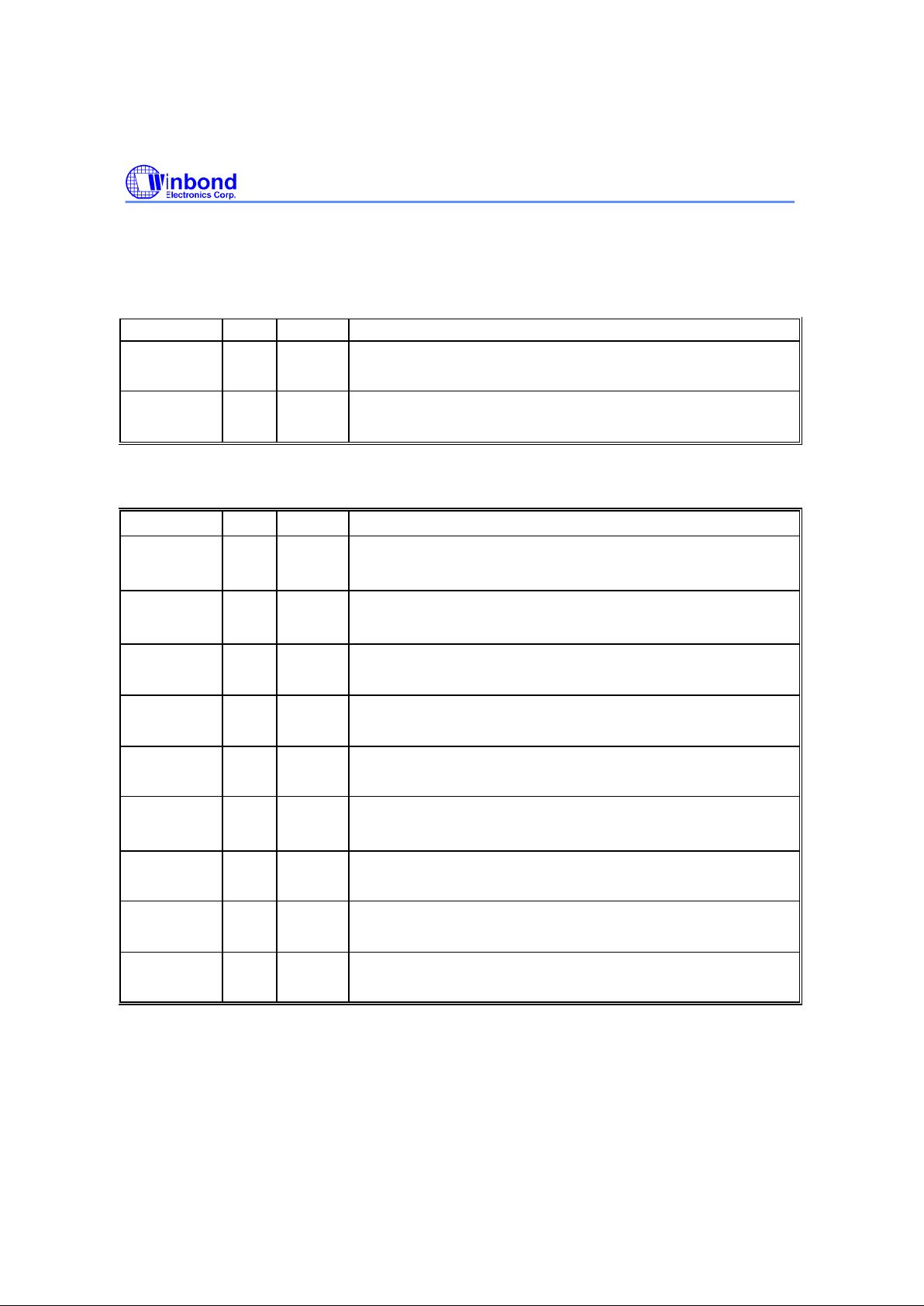
1.5 Infrared Port
SYMBOL PIN I/O FUNCTION
IRRX
64
IN
ts
Alternate Function Input: Infrared Receiver input.
General purpose I/O port 3 bit 6.
IRTX
65 OUT12t Alternate Function Output: Infrared Transmitter Output.
General purpose I/O port 3 bit 7.
1.6 Fresh ROM Interface
SYMBOL PIN I/O FUNCTION
XA18-XA16
GP57-GP55
66-68 O
I/OD
12t
Flash ROM interface Address[18:16]
General purpose I/O port 5 bit7-5
XA15-XA10
GP47-GP42
69-74 O
I/OD
12t
Flash ROM interface Address[15:10]
General purpose I/O port 4 bit7-2
XA9 -XA8
GP41-GP40
76-77 O
I/OD
12t
Flash ROM interface Addres s[9:8]
General purpose I/O port 4 bit1-0
XA7 -XA0
GP37-GP30
78-85 O
I/OD
12t
Flash ROM interface Address[7:0]
General purpose I/O port 3 bit7-0
XD7- XD4
GP27-GP24
86-89 O
I/OD
12t
Flash ROM interface Data Bus[7:4]
General purpose I/O port 2 bit7-4
XD3- XD0
GP23-GP20
91-94 O
I/OD
12t
Flash ROM interface Data Bus [3:0]
General purpose I/O port 2 bit3-0
ROMCS#
GP54
95 O
I/OD
12t
Flash ROM interface Chip Select
General purpose I/O port 5 bit4
MEMR#
GP53
96 O
I/OD
12t
Flash ROM interface Memory Read Enable
General purpose I/O port 5 bit3
MEMW#
GP52
97 O
I/OD
12t
Flash ROM interface Memory Write Enable
General purpose I/O port 5 bit2
Page 22
W83697SF
PRELIMINARY
Publication Release Date: April 2001
- 17 - Revision 0.51
1.7 General Purpose I/O Port
SYMBOL PIN I/O FUNCTION
GP73 111 I/OD
12t
General purpose I/O port 7 bit3
GP80
WDTO
118 I/OD
12t
OD12
General purpose I/O port 8 bit0
Watch dog timer output.
GP67 99 I/OD
12t
General purpose I/O port 6 bit7.
GP66 100 I/OD
12t
General purpose I/O port 6 bit6.
GP65 101 I/OD
12t
General purpose I/O port 6 bit5.
GP64 102 I/OD
12t
General purpose I/O port 6 bit4.
GP63 103 I/OD
12t
General purpose I/O port 6 bit3.
GP62 104 I/OD
12t
General purpose I/O port 6 bit2.
GP61 105 I/OD
12t
General purpose I/O port 6 bit1.
GP60 106 I/OD
12t
General purpose I/O port 6 bit0.
1.8 Smart Card Interface
SYMBOL PIN I/O FUNCTION
SCPSNT
GP77
107
IN
ts
I/OD
12t
Smart card present detection Schmitt-trigger input.
General purpose I/O port 7 bit7.
SCIO
GP76
108 I/O
12t
I/OD
12t
Smart card data I/O channel.
General purpose I/O port 7 bit6.
SCCLK
GP75
109 OUT12
I/OD
12t
Smart card clock output.
General purpose I/O port 7 bit5.
SCRST
GP74
110 OUT12
I/OD
12t
Smart card reset output.
General purpose I/O port 7 bit4.
SCC8
GP72
112 I/O
12t
I/OD
12t
Smart card General Purpose I/O channel.
General purpose I/O port 7 bit2.
SCPWR
GP71
113 OUT12
I/OD
12t
Smart card power control.
General purpose I/O port 7 bit1.
SCC4
GP70
114 I/O
12t
I/OD
12t
Smart card General Purpose I/O channel.
General purpose I/O port 7 bit0.
Page 23
W83697SF
PRELIMINARY
Publication Release Date: April 2001
- 18 - Revision 0.51
1.9 PWM & General Purpose I/O Port 8
SYMBOL PIN I/O FUNCTION
PWM2
PLED
GP83
115
OUT16t
OD
12
I/OD
12t
Fan speed control . Use the Pulse Width Modulation (PWM)
Power LED output, this signal is low after system reset.
General purpose I/O port 8 bit2-1
PWM1-0
GP82-81
116 -
117
OUT
16t
I/OD
12t
Fan speed control . Use the Pulse Width Modulation (PWM)
Technic knowledge to control the Fan’s RPM.
General purpose I/O port 8 bit2-1
1.10 Game Port & MIDI Port
SYMBOL PIN I/O FUNCTION
MSI
GP51
119 INt
I/OD12
MIDI serial data input .
General purpose I/O port 5 bit 1.
MSO
GP50
120 OUT12t
I/OD12
MIDI serial data output.
General purpose I/O port 5 bit 0.
GPAS2
GP17
121 INcs
I/OD12
Active-low, Joystick I switch input 2. This pin has an internal pull-up
resistor. (Default)
General purpose I/O port 1 bit 7.
GPBS2
GP16
122 INcs
I/OD
12
Active-low, Joystick II switch input 2. This pin has an internal pull-up
resistor. (Default)
General purpose I/O port 1 bit 6.
GPAY
GP15
123 I/OD
12
I/OD12
Joystick I timer pin. this pin connect to Y positioning variable
resistors for the Josystick. (Default)
General purpose I/O port 1 bit 5.
GPBY
GP14
124 I/OD12
I/OD12
Joystick II timer pin. this pin connect to Y positioning variable
resistors for the Josystick. (Default)
General purpose I/O port 1 bit 4.
Page 24
W83697SF
PRELIMINARY
Publication Release Date: April 2001
- 19 - Revision 0.51
1.10 Game Port & MIDI Port, continued
SYMBO L PIN I/O FUNCTION
GPBX
GP13
125 I/OD12
I/OD12
Joystick II timer pin. this pin connect to X positioning variable
resistors for the Josystick. (Default)
General purpose I/O port 1 bit 3.
GPAX
GP12
126 I/OD12
I/OD12
Joystick I timer pin. this pin connect to X positioning variable
resistors for the Josystick. (Default)
General purpose I/O port 1 bit 2.
GPBS1
GP11
127 INcs
I/OD12
Active-low, Joystick II switch input 1. This pin has an internal pull-up
resistor. (Default)
General purpose I/O port 1 bit 1.
GPAS1
GP10
128 INcs
I/OD12
Active-low, Joystick I switch input 1. This pin has an internal pull-up
resistor. (Default)
General purpose I/O port 1 bit 0.
1.11 POWER PINS
SYMBOL PIN FUNCTION
VCC 5, 45, 75, +5V power supply for the digital circuitry.
VCC3V 22 +3.3V power supply for driving 3V on host interface.
GND 18, 60, 90, Ground.
Page 25

W83697SF
PRELIMINARY
Publication Release Date: April 2001
- 20 - Revision 0.51
2.0 LPC (LOW PIN COUNT) INTERFACE
LPC interface is to replace ISA interface serving as a bus interface between host (chip-set) and
peripheral (Winbond I/O). Data transfer on the LPC bus are serialized over a 4 bit bus. The general
characteristics of the interface implemented in Winbond LPC I/O are:
• One control line, namely LFRAME#, which is used by the host to start or stop transfers. No
peripherals drive this signal.
• The LAD[3:0] bus, which communicates information serially. The information conveyed are cycle
type, cycle direction, chip selection, address, data, and wait states.
• MR (master reset) of Winbond ISA I/O is replaced with a active low reset signal, namely LRESET#, in
Winbond LPC I/O.
• An additional 33 MHz PCI clock is needed in Winbond LPC I/O for synchronization.
• DMA requests are issued through LDRQ#.
• Interrupt requests are issued through SERIRQ.
• Power management events are issued through PME#.
Comparing to its ISA counterpart, LPC implementation saves up to 40 pin counts free for integrating
more devices on a single chip.
The transition from ISA to LPC is transparent in terms of software which means no BIOS or device driver
update is needed except chip-specific configuration.
Page 26

W83697SF
PRELIMINARY
Publication Release Date: April 2001
- 21 - Revision 0.51
3.0 FDC FUNCTIONAL DESCRIPTION
3.1 W83697SF FDC
The floppy disk controller of the W83697SF integrates all of the logic required for floppy disk control. The
FDC implements a PC/AT or PS/2 solution. All programmable options default to compatible values. The
FIFO provides better system performance in multi-master systems. The digital data separator supports
up to 2 M bits/sec data rate.
The FDC includes the following blocks: AT interface, Precompensation, Data Rate Selection, Digital
Data Separator, FIFO, and FDC Core.
3.1.1 AT interface
The interface consists of the standard asynchronous signals:
RD#
, WR#, A0-A3, IRQ, DMA control, and
a data bus. The address lines select between the configuration registers, the FIFO and control/status
registers. This interface can be switched between PC/AT, Model 30, or PS/2 normal modes. The PS/2
register sets are a superset of the registers found in a PC/AT.
3.1.2 FIFO (Data)
The FIFO is 16 bytes in size and has programmable threshold values. All command parameter
information and disk data transfers go through the FIFO. Data transfers are governed by the RQM and
DIO bits in the Main Status Register.
The FIFO defaults to disabled mode after any form of reset. This maintains PC/AT hardware
compatibility. The default values can be changed through the CONFIGURE command. The advantage of
the FIFO is that it allows the system a larger DMA latency without causing disk errors. The following
tables give several examples of the delays with a FIFO. The data are based upon the following formula:
THRESHOLD # × (1/DATA/RATE) *8 - 1.5 µS = DELAY
FIFO THRESHOLD MAXIMUM DELAY TO SERVICING AT 500K BPS
Data Rate
1 Byte 1 × 16 µS - 1.5 µS = 14.5 µS
2 Byte 2 × 16 µS - 1.5 µS = 30.5 µS
8 Byte 8 × 16 µS - 1.5 µS = 6.5 µS
15 Byte 15 × 16 µS - 1.5 µ S = 238.5 µS
FIFO THRESHOLD MAXIMUM DELAY TO SERVICING AT 1M BPS
Data Rate
1 Byte 1 × 8 µ S - 1.5 µS = 6.5 µS
2 Byte 2 × 8 µ S - 1.5 µS = 14.5 µS
8 Byte 8 × 8 µS - 1.5 µS = 62.5 µS
15 Byte 15 × 8 µS - 1.5 µS = 118.5 µ S
Page 27

W83697SF
PRELIMINARY
Publication Release Date: April 2001
- 22 - Revision 0.51
At the start of a command the FIFO is always disabled and command parameters must be sent based
upon the RQM and DIO bit settings in the main status register. When the FDC enters the command
execution phase, it clears the FIFO of any data to ensure that invalid data are not transferred.
An overrun and underrun will terminate the current command and the data transfer. Disk writes will
complete the current sector by generating a 00 pattern and valid CRC. Reads require the host to remove
the remaining data so that the result phase may be entered.
DMA transfers are enabled with the SPECIFY command and are initiated by the FDC by activating the
DRQ pin during a data transfer command. The FIFO is enabled directly by asserting DACK# and
addresses need not be valid.
Note that if the DMA controller is programmed to function in verify mode a pseudo read is performed by
the FDC based only on DACK#. This mode is only available when the FDC has been configured into byte
mode (FIFO di sabled) and is programmed to do a read. With the FIFO enabled the above operation is
performed by using the new VERIFY command. No DMA operation is needed.
3.1.3 Data Separator
The function of the data separator is to lock onto the incoming serial read data. When a lock is achieved
the serial front end logic of the chip is provided with a clock which is synchronized to the read data. The
synchronized clock, called the Data Window, is used to internally sample the serial data portion of the
bit cell, and the alternate state samples the clock portion. Serial to parallel conversion logic separates
the read data into clock and data bytes.
The Digital Data Separator (DDS) has three parts: control logic, error adjustment, and speed tracking.
The DDS circuit cycles once every 12 clock cycles ideally. Any data pulse input will be synchronized
and then adjusted by immediate error adjustment. The control logic will generate RDD and RWD for
every pulse input. During any cycle where no data pulse is present, the DDS cycles are based on speed.
A digital integrator is used to keep track of the speed changes in the input data stream.
3.1.4 Write Precompensation
The write precompensation logic is used to minimize bit shifts in the RDDATA stream from the disk
drive. Shifting of bits is a known phenomenon in magnetic media and is dependent on the disk media
and the floppy drive.
The FDC monitors the bit stream that is being sent to the drive. The data patterns that require
precompensation are well known. Depending upon the pattern, the bit is shifted either early or late
relative to the surrounding bits.
Page 28

W83697SF
PRELIMINARY
Publication Release Date: April 2001
- 23 - Revision 0.51
3.1.5 Perpendicular Recording Mode
The FDC is also capable of interfacing directly to perpendicular recording floppy drives. Perpendicular
recording differs from the traditional longitudinal method in that the magnetic bits are oriented vertically.
This scheme packs more data bits into the same area.
FDCs with perpendicular recording drives can read standard 3.5" floppy disks and can read and write
perpendicular media. Some manSFacturers offer drives that can read and write standard and
perpendicular media in a perpendicular media drive.
A single command puts the FDC into perpendicular mode. All other commands operate as they normally
do. The perpendicular mode requires a 1 Mbps data rate for the FDC. At this data rate the FIFO eases
the host interface bottleneck due to the speed of data transfer to or from the disk.
3.1.6 FDC Core
The W83697SF FDC is capable of performing twenty commands. Each command is initiated by a multi byte transfer from the microprocessor. The result can also be a multi- byte transfer back to the
microprocessor. Each command consists of three phases: command, execution, and result.
Command
The microprocessor issues all required information to the controller to perform a specific operation.
Execution
The controller performs the specified operation.
Result
After the operation is completed, status information and other housekeeping information is provided to
the microprocessor.
3.1.7 FDC Commands
Command Symbol Descriptions:
C: Cylinder number 0 - 256
D: Data Pattern
DIR: Step Direction
DIR = 0, step out
DIR = 1, step in
DS0: Disk Drive Select 0
DS1: Disk Drive Select 1
DTL: Data Length
EC: Enable Count
EOT: End of Track
EFIFO: Enable FIFO
EIS: Enable Implied Seek
Page 29

W83697SF
PRELIMINARY
Publication Release Date: April 2001
- 24 - Revision 0.51
EOT: End of track
FIFOTHR: FIFO Threshold
GAP: Gap length selection
GPL: Gap Length
H: Head number
HDS: Head number select
HLT: Head Load Time
HUT: Head Unload Time
LOCK: Lock EFIFO, FIFOTHR, PTRTRK bits prevent affected by software reset
MFM: MFM or FM Mode
MT: Multitrack
N: The number of data bytes written in a sector
NCN: New Cylinder Number
ND: Non-DMA Mode
OW: Overwritten
PCN: Present Cylinder Number
POLL: Polling Disable
PRETRK: Precompensation Start Track Number
R: Record
RCN: Relative Cylinder Number
R/W: Read/Write
SC: Sector/per cylinder
SK: Skip deleted data address mark
SRT: Step Rate Time
ST0: Status Register 0
ST1: Status Register 1
ST2: Status Register 2
ST3: Status Register 3
WG: Write gate alters timing of WE
Page 30

W83697SF
PRELIMINARY
Publication Release Date: April 2001
- 25 - Revision 0.51
(1) Read Data
PHASE R/W D7 D6 D5 D4 D3 D2 D1 D0 REMARKS
Command W
MT MFM SK 0 0 1 1 0
Command codes
W
0 0 0 0 0 HDS DS1 DS0
W
W
---------------------- C ------------------------
---------------------- H ------------------------
Sector ID information prior to
command execution
W
W
---------------------- R ------------------------
---------------------- N ------------------------
W
W
-------------------- EOT -----------------------
-------------------- GPL ---------------------- W -------------------- DTL -----------------------
Execution Data transfer between the
FDD and system
Result R
R
R
-------------------- ST0 -----------------------
-------------------- ST1 -----------------------
-------------------- ST2 -----------------------
Status information after
command execution
R
R
R
R
----- ----------------- C ------------------------
---------------------- H ------------------------
---------------------- R ------------------------
---------------------- N ------------------------
Sector ID information after
command execution
Page 31

W83697SF
PRELIMINARY
Publication Release Date: April 2001
- 26 - Revision 0.51
(2) Read Deleted Data
PHASE R/W D7 D6 D5 D4 D3 D2 D1 D0 REMARKS
Command W MT MFM SK 0 1 1 0 0 Command codes
W 0 0 0 0 0 HDS DS1 DS0
W
W
---------------------- C ------------------------
---------------------- H ------------------------
Sector ID information prior to
command execution
W
W
---------------------- R ------------------------
---------------------- N ------------------------
W
W
-------------------- EOT -----------------------
-------------------- GPL -----------------------
W
-------------------- DTL -----------------------
Execution Data transfer between the
FDD and system
Result
R
R
R
-------------------- ST0 -----------------------
-------------------- ST1 -----------------------
-------------------- ST2 -----------------------
Status information after
command execution
R
R
R
R
---------------------- C ------------------------
---------------------- H ------------------------
---------------------- R ------------------------
---------------------- N ------------------------
Sector ID information after
command execution
Page 32

W83697SF
PRELIMINARY
Publication Release Date: April 2001
- 27 - Revision 0.51
(3) Read A Track
PHASE R/W D7 D6 D5 D4 D3 D2 D1 D0 REMARKS
Command W 0 MFM 0 0 0 0 1 0 Command codes
W 0 0 0 0 0 HDS DS1 DS0
W
W
---------------------- C ------------------------
---------------------- H -------------------- ----
Sector ID information prior to
command execution
W
W
---------------------- R ------------------------
---------------------- N ------------------------
W
W
-------------------- EOT -----------------------
-------------------- GPL - ----------------------
W
-------------------- DTL ----------------------Execution
Data transfer between the
FDD and system; FDD reads
contents of all cylinders from
index hole to EOT
Result
R
R
R
-------------------- ST0 -----------------------
-------------------- ST1 -----------------------
-------------------- ST2 -----------------------
Status information after
command execution
R
R
R
R
---------------------- C ------------------------
---------------------- H ---- --------------------
---------------------- R ------------------------
---------------------- N ------------------------
Sector ID information after
command execution
Page 33

W83697SF
PRELIMINARY
Publication Release Date: April 2001
- 28 - Revision 0.51
(4) Read ID
PHASE R/W D7 D6 D5 D4 D3 D2 D1 D0 REMARKS
Command W 0 MFM 0 0 1 0 1 0 Command codes
W 0 0 0 0 0 HDS DS1 DS0
Execution
The first correct ID
information on the cylinder
is stored in Data Register
Result R
R
R
-------------------- ST0 -----------------------
-------------------- ST1 -----------------------
-------------------- ST2 -----------------------
Status information after
command execution
R
R
R
R
---------------------- C ------------------ ------
---------------------- H ------------------------
---------------------- R ------------------------
---------------------- N ------------------------
Disk status after the
command has been
completed
Page 34

W83697SF
PRELIMINARY
Publication Release Date: April 2001
- 29 - Revision 0.51
(5) Verify
PHASE R/W D7 D6 D5 D4 D3 D2 D1 D0 REMARKS
Command W MT MFM SK 1 0 1 1 0 Command codes
W EC 0 0 0 0 HDS DS1 DS0
W
W
---------------------- C ------------------------
--------------------- - H ------------------------
Sector ID information prior
to command execution
W
W
---------------------- R ------------------------
---------------------- N ------------------------
W
W
-------------------- EOT -----------------------
-------------------- GPL -----------------------
-------------------- DTL/SC -------------------
Execution No data transfer takes
place
Result R
R
R
-------------------- ST0 -----------------------
-------------------- ST1 -----------------------
-------------------- ST2 -----------------------
Status information after
command execution
R
R
R
R
---------------------- C ------------------------
---------------------- H ------------------------
---------------------- R ------------- -----------
---------------------- N ------------------------
Sector ID information after
command execution
Page 35

W83697SF
PRELIMINARY
Publication Release Date: April 2001
- 30 - Revision 0.51
(6) Version
PHASE R/W D7 D6 D5 D4 D3 D2 D1 D0 REMARKS
Command
W 0 0 0 1 0 0 0 0
Command code
Result
R 1 0 0 1 0 0 0 0
Enhanced controller
(7) Write Data
PHASE R/W D7 D6 D5 D4 D3 D2 D1 D0 REMARKS
Command W MT MFM 0 0 0 1 0 1 Command codes
W 0 0 0 0 0 HDS DS1 DS0
W
W
---------------------- C ------------------------
---------------------- H ------------------------
Sector ID information prior
to Command execution
W
W
---------------------- R ------------------------
---------------------- N ------------------------
W
W
-------------------- EOT -----------------------
-------------------- GPL -----------------------
W
-------------------- DTL -----------------------
Execution Data transfer between the
FDD and system
Result R
R
R
-------------------- ST0 -----------------------
-------------------- ST1 -----------------------
-------------------- ST2 -----------------------
Status information after
Command execution
R
R
R
R
---------------------- C ------------------------
---------------------- H ------------------------
---------------------- R ------------------------
---------------------- N ------------------- -----
Sector ID information after
Command execution
Page 36

W83697SF
PRELIMINARY
Publication Release Date: April 2001
- 31 - Revision 0.51
(8) Write Deleted Data
PHASE R/W D7 D6 D5 D4 D3 D2 D1 D0 REMARKS
Command W MT MFM 0 0 1 0 0 1 Command codes
W 0 0 0 0 0 HDS DS1 DS0
W
W
---------------------- C ------------------------
---------------------- H ------------------------
Sector ID information prior
to command execution
W
W
---------------------- R ------------------------
---------------------- N ------------------------
W
W
W
-------------------- EOT -----------------------
-------------------- GPL -----------------------
-------------------- DTL -----------------------
Execution Data transfer between the
FDD and system
Result R
R
R
-------------------- ST0 -----------------------
-------------------- ST1 -----------------------
-------------------- ST2 -----------------------
Status information after
command execution
R
R
R
R
---------------------- C ------------------------
---------------------- H ------------------------
---------------------- R ------------------------
---------------------- N ------------------------
Sector ID information after
command execution
Page 37
W83697SF
PRELIMINARY
Publication Release Date: April 2001
- 32 - Revision 0.51
(9) Format A Track
PHASE R/W D7 D6 D5 D4 D3 D2 D1 D0 REMARKS
Command W 0 MFM 0 0 1 1 0 1 Command codes
W 0 0 0 0 0 HDS DS1 DS0
W
W
---------------------- N ------------------------
--------------------- SC -----------------------
Bytes/Sector
Sectors/Cylinder
W
W
--------------------- GPL ---------------------
---------------------- D ------------------------
Gap 3
Filler Byte
Execution
for Each
Sector
Repeat:
W
W
W
W
---------------------- C ------------------------
---------------------- H ------------------------
---------------------- R ------------------------
---------------------- N ------------------------
Input Sector Parameters
Result R
R
R
-------------------- ST0 -----------------------
-------------------- ST1 -----------------------
-------------------- ST2 -----------------------
Status information after
command execution
R
R
R
R
---------------- Undefined ------------ -------
---------------- Undefined -------------------
---------------- Undefined -------------------
---------------- Undefined -------------------
(10) Recalibrate
PHASE R/W D7 D6 D5 D4 D3 D2 D1 D0 REMARKS
Command W 0 0 0 0 0 1 1 1 Command codes
W 0 0 0 0 0 0 DS1 DS0
Execution Head retracted to Track 0
Interrupt
(11) Sense Interrupt Status
PHASE R/W D7 D6 D5 D4 D3 D2 D1 D0 REMARKS
Command W 0 0 0 0 1 0 0 0 Command code
Result
R
R
---------------- ST0 -------------------------
---------------- PCN -------------------------
Status information at the end
of each seek operation
Page 38
W83697SF
PRELIMINARY
Publication Release Date: April 2001
- 33 - Revision 0.51
(12) Specify
PHASE R/W D7 D6 D5 D4 D3 D2 D1 D0 REMARKS
Command W 0 0 0 0 0 0 1 1 Command codes
W
W
| --------- SRT ----------- | --------- HUT ---------- |
|------------ HLT ----------------------------------| ND
(13) Seek
PHASE R/W D7 D6 D5 D4 D3 D2 D1 D0 REMARKS
Command W 0 0 0 0 1 1 1 1
Command codes
W W 0 0 0 0 0 HDS DS1 DS0
-------------------- NCN -----------------------
Execution R Head positioned over proper
cylinder on diskette
(14) Configure
PHASE R/W D7 D6 D5 D4 D3 D2 D1 D0 REMARKS
Command W 0 0 0 1 0 0 1 1 Configure information
W
W
W
0 0 0 0 0 0 0 0
0 EIS EFIFO POLL | ------ FIFOTHR ---- |
| --------------------PRETRK ----------------------- |
Execution Internal registers written
(15) Relative Seek
PHASE R/W D7 D6 D5 D4 D3 D2 D1 D0 REMARKS
Command W 1 DIR 0 0 1 1 1 1 Command codes
W
W
0 0 0 0 0 HDS DS1 DS0
| -------------------- RCN ---------------------------- |
Page 39
W83697SF
PRELIMINARY
Publication Release Date: April 2001
- 34 - Revision 0.51
(16) Dumpreg
PHASE R/W D7 D6 D5 D4 D3 D2 D1 D0 REMARKS
Command W 0 0 0 0 1 1 1 0 Registers placed in FIFO
Result
R
R
R
R
R
R
R
R
R
R
----------------------- PCN -Drive 0--------------------
----------------------- PCN -Drive 1 -------------------
----------------------- PCN -Drive 2--------------------
----------------------- PCN -Drive 3 -------------------
--------SRT ------------------ | --------- HUT --------
----------- HLT -----------------------------------| ND
------------------------ SC/EOT ----------------------
LOCK 0 D3 D2 D1 D0 GAP WG
0 EIS EFIFO POLL | ------ FIFOTHR --------
-----------------------PRETRK -------------------------
(17) Perpendicular Mode
PHASE R/W D7 D6 D5 D4 D3 D2 D1 D0 REMARKS
Command W 0 0 0 1 0 0 1 0 Command Code
W OW 0 D3 D2 D1 D0 GAP WG
(18) Lock
PHASE R/W D7 D6 D5 D4 D3 D2 D1 D0 REMARKS
Command W LOCK 0 0 1 0 1 0 0 Command Code
Result R 0 0 0 LOCK 0 0 0 0
(19) Sense Drive Status
PHASE R/W D7 D6 D5 D4 D3 D2 D1 D0 REMARKS
Command W 0 0 0 0 0 1 0 0 Command Code
W 0 0 0 0 0 HDS DS1 DS0
Result
R
---------------- ST3 -------------------------
Status information about
disk drive
(20) Invalid
PHASE R/W D7 D6 D5 D4 D3 D2 D1 D0 REMARKS
Command W ------------- Invalid Codes --------- -------- Invalid codes (no operation-
FDC goes to standby state)
Page 40

W83697SF
PRELIMINARY
Publication Release Date: April 2001
- 35 - Revision 0.51
Result R
-------------------- ST0 ----------------------
ST0 = 80H
Page 41
W83697SF
PRELIMINARY
Publication Release Date: April 2001
- 36 - Revision 0.51
3.2 Register Descriptions
There are several status, data, and control registers in W83697SF. These registers are defined below:
ADDRESS REGISTER
OFFSET READ WRITE
base address + 0
base address + 1
base address + 2
base address + 3
SA REGISTER
SB REGISTER
TD REGISTER
DO REGISTER
TD REGISTER
base address + 4 MS REGISTER DR REGISTER
base address + 5 DT (FIFO) REGISTER DT (FIFO) REGISTER
base address + 7 DI REGISTER CC REGISTER
3.2.1 Status Register A (SA Register) (Read base address + 0)
This register is used to monitor several disk interface pins in PS/2 and Model 30 modes. In PS/2 mode,
the bit definitions for this register are as follows:
1
2
34567
0
WP
INDEX
HEAD
TRAK0
STEP
DRV2
INIT PENDING
DIR
INIT PENDING (Bit 7):
This bit indicates the value of the floppy disk interrupt output.
DRV2#
(Bit 6):
0 A sec ond drive has been installed
1
A second drive has not been installed
STEP (Bit 5):
This bit indicates the complement of STEP# output.
TRAK0#
(Bit 4):
Page 42
W83697SF
PRELIMINARY
Publication Release Date: April 2001
- 37 - Revision 0.51
This bit indicates the value of TRAK0# input.
HEAD (Bit 3):
This bit indicates the complement of HEAD# output.
0 side 0
1 side 1
INDEX#
(Bit 2):
This bit indicates the value of
INDEX#
output.
WP# (Bit 1):
0 disk is write-protected
1 disk is not write-protected
DIR (Bit 0)
This bit indicates the direction of head movement.
0 outward direction
1 inward direction
In PS/2 Model 30 mode, the bit definitions for this register are as follows:
1
2
34567
0
WP
INDEX
HEAD
TRAK0
STEP F/F
DRQ
INIT PENDING
DIR
INIT PENDING (Bit 7):
This bit indicates the value of the floppy disk interrupt output.
DRQ (Bit 6):
This bit indicate s the value of DRQ output pin.
STEP F/F (Bit 5):
Page 43
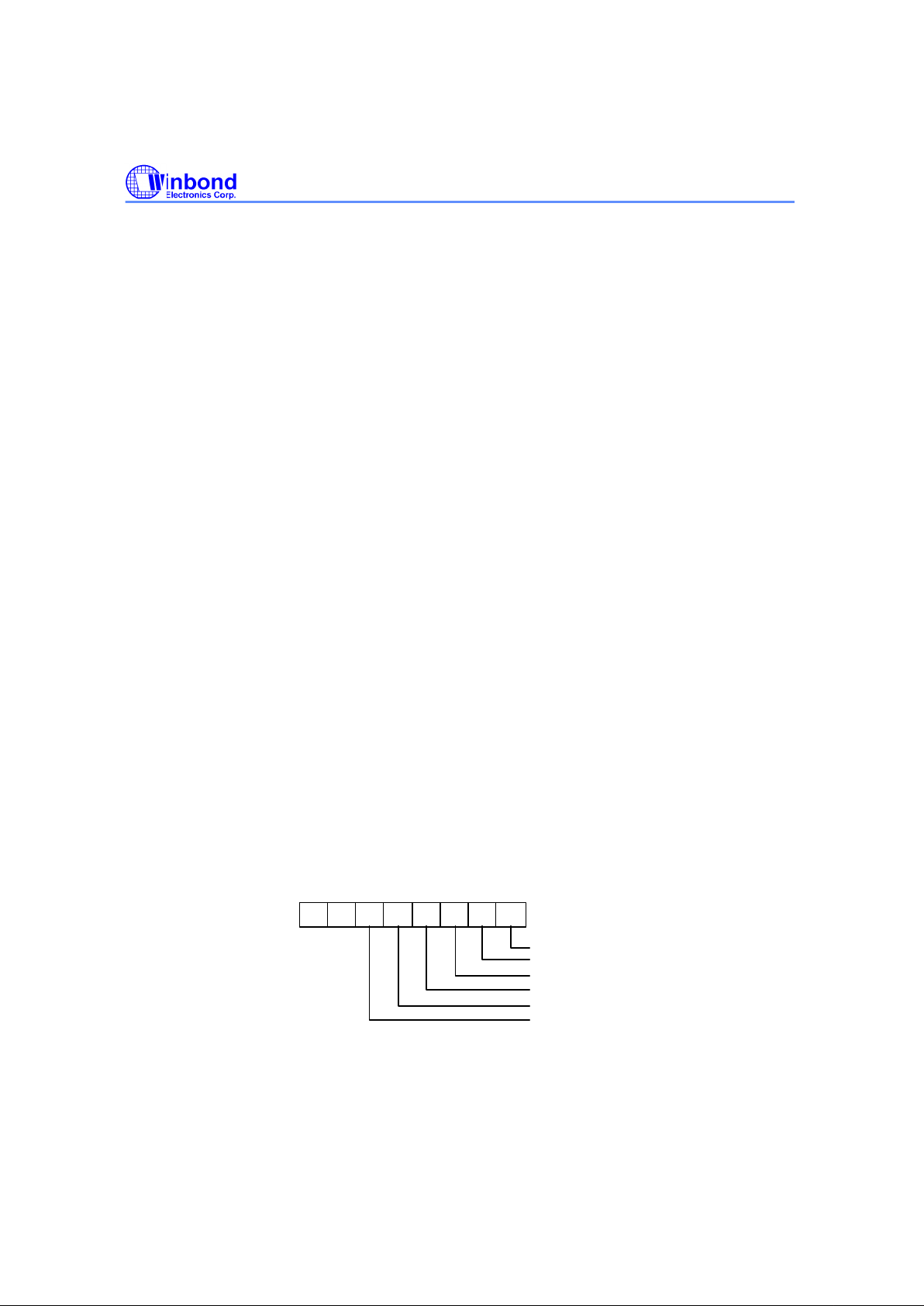
W83697SF
PRELIMINARY
Publication Release Date: April 2001
- 38 - Revision 0.51
This bit indicates the complement of latched STEP# output.
TRAK0 (Bit 4):
This bit indicates the complement of TRAK0# input.
HEAD#
(Bit 3):
This bit indicates the value of
HEAD#
output.
0 side 1
1 side 0
INDEX (Bit 2):
This bit indicates the complement of INDEX# output.
WP (Bit 1):
0 disk is not write-protected
1 disk is write-protected
DIR#
(Bit 0)
This bit indicates the direction of head movement.
0 inward direction
1 outward direction
3.2.2 Status Register B (SB Register) (Read base address + 1)
This register is used to monitor several disk interface pins in PS/2 and Model 30 modes. In PS/2 mode,
the bit definitions for this register are as follows:
1
2
34567
0
MOT EN A
WE
RDATA Toggle
WDATA Toggle
Drive SEL0
MOT EN B
1
1
Drive SEL0 (Bit 5):
This bit indicates the status of DO REGISTER bit 0 (drive select bit 0).
Page 44
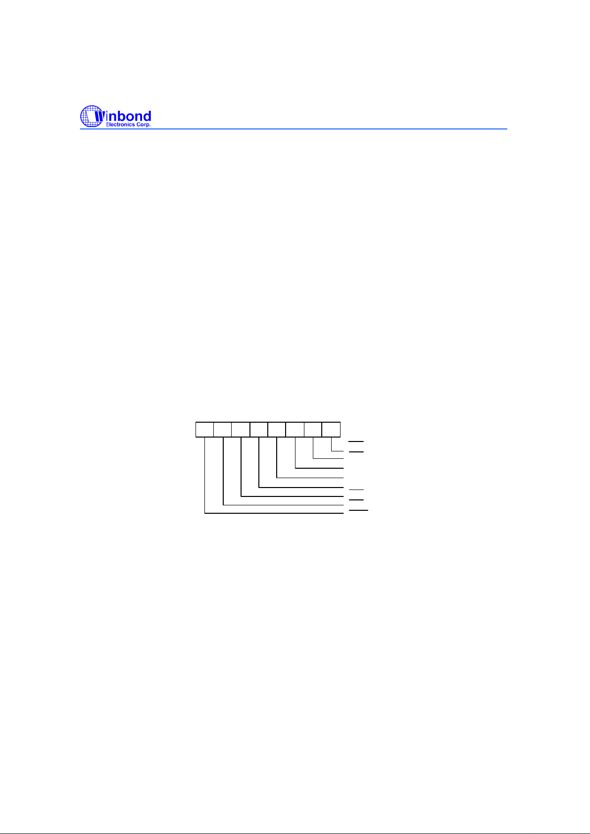
W83697SF
PRELIMINARY
Publication Release Date: April 2001
- 39 - Revision 0.51
WDATA Toggle (Bit 4):
This bit changes state at every rising edge of the
WD#
output pin.
RDATA Toggle (Bit 3):
This bit changes state at every rising edge of the
RDATA#
output pin.
WE (Bit 2):
This bit indicates the complement of the
WE#
output pin.
MOT EN B (Bit 1)
This bit indicates the complement of the
MOB#
output pin.
MOT EN A (Bit 0)
This bit indicates the complement of the
MOA#
output pin.
In PS/2 Model 30 mode, the bit definitions for this register are as follows:
1
2
34567
0
DSC
DSD
WE F/F
RDATA F/F
DSA
DSB
DRV2
WD F/F
DRV2#
(Bit 7):
0 A second drive has been installed
1 A second drive has not been installed
DSB#
(Bit 6):
This bit indicates the status of
DSB#
output pin.
DSA# (Bit 5):
This bit indicates the status of DSA# output pin.
Page 45

W83697SF
PRELIMINARY
Publication Release Date: April 2001
- 40 - Revision 0.51
WD F/F(Bit 4):
This bit indicates the complement of the latched WD# output pin at every rising edge of the WD# output
pin.
RDATA F/F(Bit 3):
This bit indicates the complement of the latched RDATA# output pin .
WE F/F (Bit 2):
This bit indicates the complement of latched WE# output pin.
DSD#
(Bit 1):
0 Drive D has been selected
1 Drive D has not been selected
DSC#
(Bit 0):
0 Drive C has been selected
1 Drive C has not been selected
3.2.3 Digital Output Register (DO Register) (Write base address + 2)
The Digital Output Register is a write-only register controlling drive motors, drive selection, DRQ/IRQ
enable, and FDC resetting. All the bits in this register are cleared by the MR pin. The bit definitions are
as follows:
7 6
5 4
3
2
1-0
Drive Select: 00 select drive A
01 select drive B
10 select drive C
11 select drive D
Floppy Disk Controller Reset
Active low resets FDC
DMA and INT Enable
Active high enable DRQ/IRQ
Motor Enable A. Motor A on when active high
Motor Enable B. Motor B on when active high
Motor Enable C. Motor C on when active high
Motor Enable D. Motor D on when active high
3.2.4. Tape Drive Register (TD Register) (Read base address + 3)
This register is used to assign a particular drive number to the tape drive support mode of the data
separator. This register also holds the media ID, drive type, and floppy boot drive information of the fl oppy
Page 46
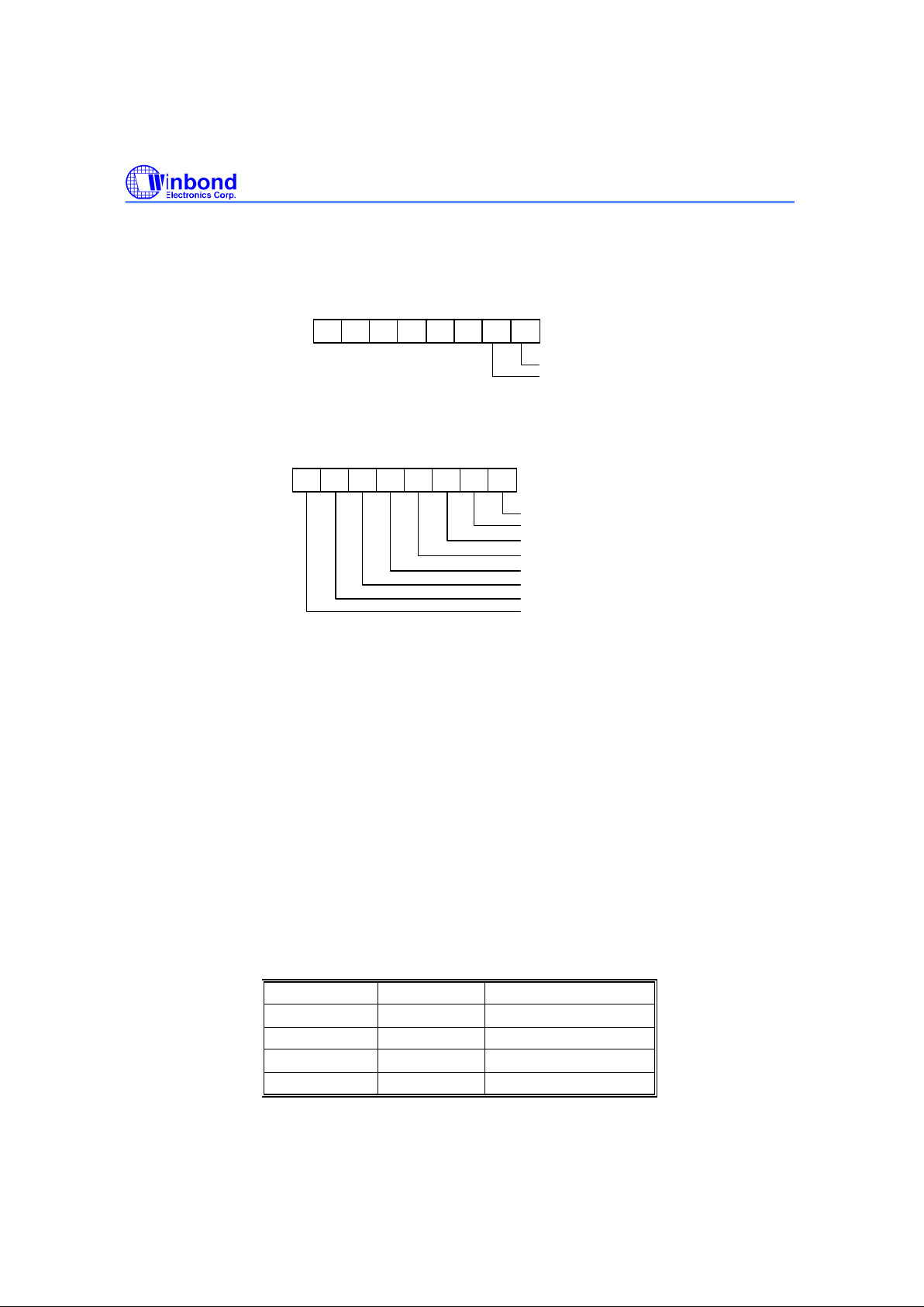
W83697SF
PRELIMINARY
Publication Release Date: April 2001
- 41 - Revision 0.51
disk drive. In normal floppy mode, this register includes only bit 0 and 1. The bit definitions are as
follows:
1
2
34567
0
Tape sel 0
Tape sel 1
X X
X X X X
If three mode FDD function is enabled (EN3MODE = 1 in CR9), the bit definitions are as follows:
1
2
34567
0
Floppy boot drive 0
Floppy boot drive 1
Drive type ID0
Drive type ID1
Media ID0
Media ID1
Tape Sel 0
Tape Sel 1
Media ID1 Media ID0 (Bit 7, 6):
Thes e two bits are read only. These two bits reflect the value of CR8 bit 3, 2.
Drive type ID1 Drive type ID0 (Bit 5, 4):
These two bits reflect two of the bits of CR7. Which two bits are reflected depends on the last drive
selected in the DO REGISTER.
Floppy Boot drive 1, 0 (Bit 3, 2):
These two bits reflect the value of CR8 bit 1, 0.
Tape Sel 1, Tape Sel 0 (Bit 1, 0):
These two bits assign a logical drive number to the tape drive. Drive 0 is not available as a tape drive and
is reserved as the floppy disk boot drive.
TAPE SEL 1 TAPE SEL 0 DRIVE SELECTED
0 0 None
0 1 1
1 0 2
1 1 3
Page 47

W83697SF
PRELIMINARY
Publication Release Date: April 2001
- 42 - Revision 0.51
Page 48
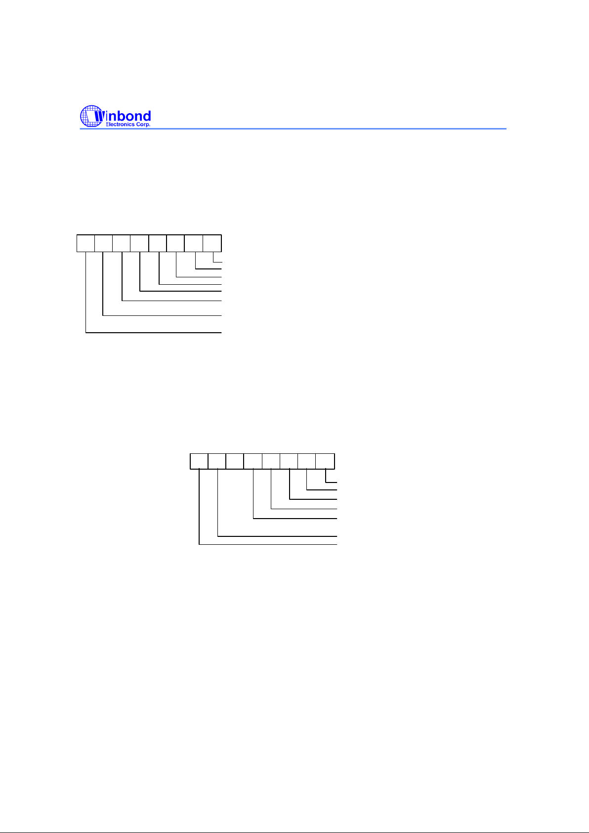
W83697SF
PRELIMINARY
Publication Release Date: April 2001
- 43 - Revision 0.51
3.2.5 Main Status Register (MS Register) (Read base address + 4)
The Main Status Register is used to control the flow of data between the microproces sor and the
controller. The bit definitions for this register are as follows:
FDD 0 Busy, (D0B = 1), FDD number 0 is in the SEEK mode.
FDD 1 Busy, (D1B = 1), FDD number 1 is in the SEEK mode.
FDC Busy, (CB). A read or write command is in the process when CB = HIGH.
Non-DMA mode, the FDC is in the non-DMA mode, this bit is set only during the
execution phase in non-DMA mode.
Transition to LOW state indicates execution phase has ended.
DATA INPUT/OUTPUT, (DIO). If DIO= HIGH then transfer is from Data Register to the processor.
If DIO = LOW then transfer is from processor to Data Register.
Request for Master (RQM). A high on this bit indicates Data Register is ready to send or receive data to or from the processor.
7
6
5 4 3 2 1
0
FDD 2 Busy, (D2B = 1), FDD number 2 is in the SEEK mode.
FDD 3 Busy, (D3B = 1), FDD number 3 is in the SEEK mode.
3.2.6 Data Rate Register (DR Register) (Write base address + 4)
The Data Rate Register is used to set the transfer rate and write precompensation. The data rate of the
FDC is programmed by the CC REGISTER for PC-AT and PS/2 Model 30 and PS/2 mode, and not by
the DR REGISTER. The real data rate is determined by the most recent write to either of the DR
REGISTER or CC REGISTER.
1
2
34567
0
DRATE0
DRATE1
PRECOMP0
PRECOMP1
PRECOMP2
POWER DOWN
S/W RESET
0
S/W RESET (Bit 7):
This bit is the software reset bit.
POWER-DOWN (Bit 6):
0 FDC in normal mode
1 FDC in power-down mode
PRECOMP2 PRECOMP1 PRECOMP0 (Bit 4, 3, 2):
These three bits select the value of write precompensation. The following tables show the
precompensation values for the combination of these bits.
Page 49
W83697SF
PRELIMINARY
Publication Release Date: April 2001
- 44 - Revision 0.51
PRECOMP PRECOMPENSATION DELAY
2 1 0 250K - 1 Mbps 2 Mbps Tape drive
0 0 0 Default Delays Default Delays
0 0 1 41.67 nS 20.8 nS
0 1 0 83.34 nS 41.17 nS
0 1 1 125.00 nS 62.5nS
1 0 0 166.67 nS 83.3 nS
1 0 1 208.33 nS 104.2 nS
1 1 0 250.00 nS 125.00 nS
1 1 1 0.00 nS (disabled) 0.00 nS (disabled)
DATA RATE DEFAULT PRECOMPENSATION DELAYS
250 KB/S 125 nS
300 KB/S 125 nS
500 KB/S 125 nS
1 MB/S 41.67nS
2 MB/S 20.8 nS
DRATE1 DRATE0 (Bit 1, 0):
These two bits select the data rate of the FDC and reduced write current control.
00
500 KB/S (MFM), 250 KB/S (FM), RWC = 1
01
300 KB/S (MFM), 150 KB/S (FM),
RWC
= 0
10
250 KB/S (MFM), 125 KB/S (FM),
RWC
= 0
11
1 MB/S (MFM), Illegal (FM),
RWC
= 1
The 2 MB/S data rate for Tape drive is only supported by setting 01 to DRATE1 and DRATE0 bits, as
well as setting 10 to DRT1 and DRT0 bits which are two of the Configure Register CRF4 or CRF5 bits in
logic device 0. Please refer to the function description of CRF4 or CRF5 and data rate table for individual
data rates setting.
Page 50
W83697SF
PRELIMINARY
Publication Release Date: April 2001
- 45 - Revision 0.51
3.2.7 FIFO Register (R/W base address + 5)
The Data Register consists of four status registers in a stack with only one register presented to the
data bus at a time. This register stores data, commands, and parameters and provides diskette- drive
status information. Data bytes are passed through the data register to program or obtain results after a
command. In the W83697SF, this register defaults to FIFO disabled mode after reset. The FIFO can
change its value and enable its operation through the CONFIGURE command.
Status Register 0 (ST0)
7-6 5
4
3 2 1-0
US1, US0 Drive Select:
00 Drive A selected
01 Drive B selected
10 Drive C selected
11 Drive D selected
HD Head address:
1 Head selected
0 Head selected
NR Not Ready:
1 Drive is not ready
0 Drive is ready
EC Equipment Check:
1 When a fault signal is received from the FDD or the track
0 signal fails to occur after 77 step pulses
0 No error
SE Seek end:
1 seek end
0 seek error
IC Interrupt Code:
00 Normal termination of command
01 Abnormal termination of command
10 Invalid command issue
11 Abnormal termination because the ready signal from FDD changed state during command execution
Status Register 1 (ST1)
Missing Address Mark. 1 When the FDC cannot detect the data address mark
or the data address mark has been deleted.
NW (Not Writable). 1 If a write Protect signal is detected from the diskette drive during
execution of write data.
ND (No DATA). 1 If specified sector cannot be found during execution of a read, write or verifly data.
Not used. This bit is always 0.
OR (Over Rum). 1 If the FDC is not serviced by the host system within a certain time interval during data transfer.
DE (data Error).1 When the FDC detects a CRC error in either the ID field or the data field.
Not used. This bit is always 0.
EN (End of track). 1 When the FDC tries to access a sector beyond the final sector of a cylinder.
01
234567
Page 51
W83697SF
PRELIMINARY
Publication Release Date: April 2001
- 46 - Revision 0.51
Status Register 2 (ST2)
1234567
0
BC (Bad Cylinder)
MD (Missing Address Mark in Data Field).
1 If the FDC cannot find a data address mark
(or the address mark has been deleted)
when reading data from the media
0 No error
1 Bad Cylinder
0 No error
SN (Scan Not satisfied)
1 During execution of the Scan command
0 No error
SH (Scan Equal Hit)
1 During execution of the Scan command, if the equal condition is satisfied
0 No error
WC (Wrong Cylinder)
1 Indicates wrong Cylinder
DD (Data error in the Data field)
1 If the FDC detects a CRC error in the data field
0 No error
CM (Control Mark)
1 During execution of the read data or scan command
0 No error
Not used. This bit is always 0
Status Register 3 (ST3)
12
3
4
5
6
7
0
US0 Unit Select 0
US1 Unit Select 1
HD Head Address
TS Two-Side
TO Track 0
RY Ready
WP Write Protected
FT Fault
3.2.8 Digital Input Register (DI Register) (Read base address + 7)
The Digital Input Register is an 8-bit read-only register used for diagnostic purposes. In a PC/XT or AT
only Bit 7 is checked by the BIOS. When the register is read, Bit 7 shows the complement of
DSKCHG#, while other bits of the data bus remain in tri-state. Bit definitions are as follows:
xxx
x
xxx
x
01234
567
Reserved for the hard disk controller
During a read of this register, these bits are in tri-state
DSKCHG
In the PS/2 mode, the bit definitions are as follows:
Page 52
W83697SF
PRELIMINARY
Publication Release Date: April 2001
- 47 - Revision 0.51
1
234567
0
HIGH DENS
DRATE0
DRATE1
DSKCHG
1 11 1
DSKCHG (Bit 7):
This bit indicates the complement of the DSKCHG# input.
Bit 6 -3: These bits are always a logic 1 during a read.
DRATE1 DRATE0 (Bit 2, 1):
These two bits select the data rate of the FDC. Refer to the DR register bits 1 and 0 for the settings
corresponding to the individual data rates.
HIGH DENS#
(Bit 0):
0 500 KB/S or 1 MB/S data rate (high density FDD)
1 250 KB/S or 300 KB/S data rate
In the PS/2 Model 30 mode, the bit definitions are as follows:
1
23456
7
0
DRATE0
DRATE1
DSKCHG
NOPREC
DMAEN
0 00
DSKCHG (Bit 7):
This bit indicates the status of DSKCHG# input.
Bit 6 -4: These bits are always a logic 1 during a read.
DMAEN (Bit 3):
This bit indicates the value of DO REGISTER bit 3.
Page 53
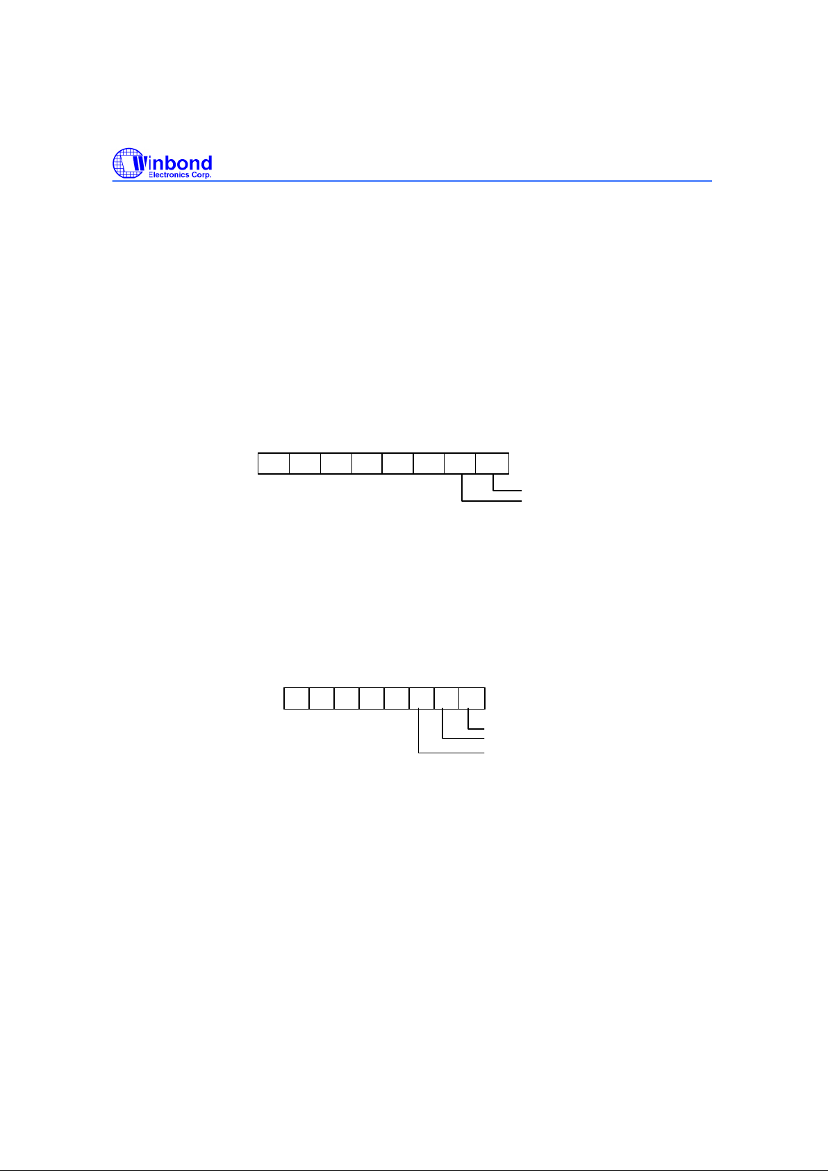
W83697SF
PRELIMINARY
Publication Release Date: April 2001
- 48 - Revision 0.51
NOPREC (Bit 2):
This bit indicates the value of CC REGISTER NOPREC bit.
DRATE1 DRATE0 (Bit 1, 0):
These two bits select the data rate of the FDC.
3.2.9 Configuration Control Register (CC Register) (Write base address + 7)
This register is used to control the data rate. In the PC/AT and PS/2 mode, the bit definitions are as
follows:
x x x x x x
DRATE0
DRATE1
0
1
2
3
4
5
7
6
X: Reserved
Bit 7- 2: Reserved. These bits should be set to 0.
DRATE1 DRATE0 (Bit 1, 0):
These two bits select the data rate of the FDC.
In the PS/2 Model 30 mode, the bit definitions are as follows:
1
2
34567
0
DRATE0
DRATE1
NOPREC
X X
X X X
X: Reserved
Bit 7- 3: Reserved. These bits should be set to 0.
NOPREC (Bit 2):
This bit indicates no precompensation. It has no function and can be set by software.
DRATE1 DRATE0 (Bit 1, 0):
These two bits select the data rate of the FDC.
Page 54
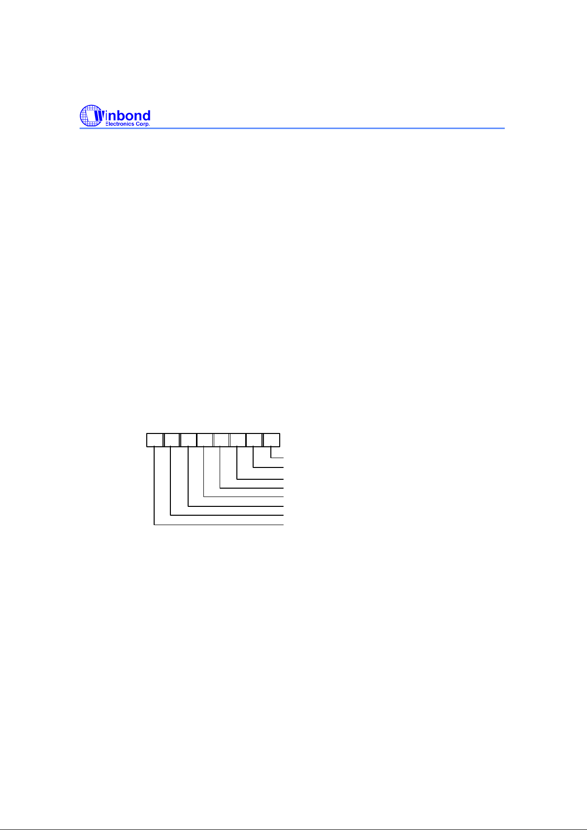
W83697SF
PRELIMINARY
Publication Release Date: April 2001
- 49 - Revision 0.51
4.0 UART PORT
4.1 Universal Asynchronous Receiver/Transmitter (UART A, UART B)
The UARTs are used to convert parallel data into serial format on the transmit side and convert serial
data to parallel format on the receiver side. The serial format, in order of transmission and reception, is a
start bit, followed by five to eight data bits, a parity bit (if programmed) and one, one and half (five-bit
format only) or two stop bits. The UARTs are capable of handling divisors of 1 to 65535 and producing a
16x clock for driving the internal transmitter logic. Provisions are also inc luded to use this 16x clock to
drive the receiver logic. The UARTs also support the MIDI data rate. Furthermore, the UARTs also
include complete modem control capability and a processor interrupt system that may be software
trailed to the computing time required to handle the communication link. The UARTs have a FIFO mode
to reduce the number of interrupts presented to the CPU. In each UART, there are 16-byte FIFOs for
both receive and transmit mode.
4.2 Register Address
4.2.1 UART Control Register (UCR) (Read/Write)
The UART Control Register controls and defines the protocol for asynchronous data communications,
including data length, stop bit, parity, and baud rate selection.
1234567 0
Data length select bit 0 (DLS0)
Data length select bit 1(DLS1)
Multiple stop bits enable (MSBE)
Parity bit enable (PBE)
Even parity enable (EPE)
Parity bit fixed enable (PBFE)
Set silence enable (SSE)
Baudrate divisor latch access bit (BDLAB)
Bit 7 BDLAB. When this bit is set to a logical 1, designers can access the divisor (in 16-
bit binary
format) from the divisor latches of the baudrate generator during a read or write operation.
When this bit is reset, the Receiver BSFfer Register, the Transmitter BSFfer Register, or the
Interrupt Control Register can be accessed.
Bit 6
SSE. A logical 1 forces the Serial Output (SOUT) to a silent state (a logical 0). Only IRTX is
affected by this bit; the transmitter is not affected.
Bit 5 PBFE. When PBE and PBFE of UCR are both set to a logical 1,
(1) if EPE is logical 1, the parity bit is fixed as logical 0 to transmit and check.
(2) if EPE is logical 0, the parity bit is fixed as logical 1 to transmit and check.
Page 55

W83697SF
PRELIMINARY
Publication Release Date: April 2001
- 50 - Revision 0.51
TABLE 4-1 UART Register Bit Map
Bit Number
Register Address Base 0 1 2 3 4 5 6 7
+ 0
BDLAB = 0
Receiver
BSFfer
Register
(Read Only)
RBR RX Data
Bit 0
RX Data
Bit 1
RX Data
Bit 2
RX Data
Bit 3
RX Data
Bit 4
RX Data
Bit 5
RX Data
Bit 6
RX Data
Bit 7
+ 0
BDLAB = 0
Transmitter
BSFfer Register
(Write Only)
TBR TX Data
Bit 0
TX Data
Bit 1
TX Data
Bit 2
TX Data
Bit 3
TX Data
Bit 4
TX Data
Bit 5
TX Data
Bit 6
TX Data
Bit 7
+ 1
BDLAB = 0
Interrupt Control
Register
ICR RBR Data
Ready
Interrupt
Enable
(ERDRI)
TBR
Empty
Interrupt
Enable
(ETBREI)
USR
Interrupt
Enable
(EUSRI)
HSR
Interrupt
Enable
(EHSRI)
0 0 0 0
+ 2 Interrupt Status
Register
(Read Only)
ISR "0" if
Interrupt
Pending
Interrupt
Status
Bit (0)
Interrupt
Status
Bit (1)
Interrupt
Status
Bit (2)**
0 0 FIFOs
Enabled
**
FIFOs
Enabled
**
+ 2 UART FIFO
Control
Register
(Write Only)
SFR FIFO
Enable
RCVR
FIFO
Reset
XMIT
FIFO
Reset
DMA
Mode
Select
Reserved Reversed RX
Interrupt
Active Level
(LSB)
RX
Interrupt
Active Level
(MSB)
+ 3 UART Control
Register
UCR Data
Length
Select
Bit 0
(DLS0)
Data
Length
Select
Bit 1
(DLS1)
Multiple
Stop Bits
Enable
(MSBE)
Parity
Bit
Enable
(PBE)
Even
Parity
Enable
(EPE)
Parity
Bit Fixed
Enable
PBFE)
Set
Silence
Enable
(SSE)
Baudrate
Divisor
Latch
Access Bit
(BDLAB)
+ 4 Handshake
Control
Register
HCR Data
Terminal
Ready
(DTR)
Request
to
Send
(RTS)
Loopback
RI
Input
IRQ
Enable
Internal
Loopback
Enable
0 0 0
+ 5 UART Status
Register
USR RBR Data
Ready
(RDR)
Overrun
Error
(OER)
Parity Bit
Error
(PBER)
No Stop
Bit
Error
(NSER)
Silent
Byte
Detected
(SBD)
TBR
Empty
(TBRE)
TSR
Empty
(TSRE)
RX FIFO
Error
Indication
(RFEI) **
+ 6 Handshake
Status Register
HSR CTS
Toggling
(TCTS)
DSR
Toggling
(TDSR)
RI Falling
Edge
(FERI)
DCD
Toggling
(TDCD)
Clear
to Send
(CTS)
Data Set
Ready
(DSR)
Ring
Indicator
(RI)
Data Carrier
Detect
(DCD)
+ 7 User Defined
Register
UDR Bit 0 Bit 1 Bit 2 Bit 3 Bit 4 Bit 5 Bit 6 Bit 7
+ 0
BDLAB = 1
Baudrate
Divisor Latch
Low
BLL Bit 0 Bit 1 Bit 2 Bit 3 Bit 4 Bit 5 Bit 6 Bit 7
+ 1
BDLAB = 1
Baudrate
Divisor Latch
High
BHL Bit 8 Bit 9 Bit 10 Bit 11 Bit 12 Bit 13 Bit 14 Bit 15
*: Bit 0 is the least significant bit. The least significant bit is the first bit serially transmitted or received.
Page 56
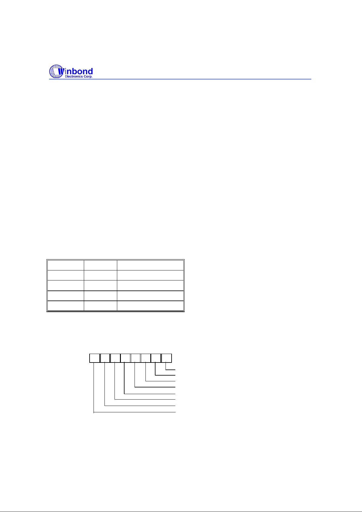
W83697SF
PRELIMINARY
Publication Release Date: April 2001
- 51 - Revision 0.51
**: These bits are always 0 in 16450 Mode.
Bit 4 EPE. This bit describes the number of logic 1's in the data word bits and parity bit on
ly when
bit 3 is programmed. When this bit is set, an even number of logic 1's are sent or checked.
When the bit is reset, an odd number of logic 1's are sent or checked.
Bit 3 PBE. When this bit is set, the position between the last data bit and the sto
p bit of the
SOUT will be stSFfed with the parity bit at the transmitter. For the receiver, the parity bit in
the same position as the transmitter will be detected.
Bit 2 MSBE. This bit defines the number of stop bits in each serial character that is tra
nsmitted or
received.
(1) If MSBE is set to a logical 0, one stop bit is sent and checked.
(2)
If MSBE is set to a logical 1, and data length is 5 bits, one and a half stop bits are sent
and checked.
(3) If MSBE is set to a logical 1, and data length is 6, 7, or
8 bits, two stop bits are sent and
checked.
Bits 0
and 1
DLS0, DLS1. These two bits define the number of data bits that are sent or checked in each
serial character.
TABLE 4-2 WORD LENGTH DEFINITION
DLS1 DLS0 DATA LENGTH
0 0 5 bits
0 1 6 bits
1 0 7 bits
1 1 8 bits
4.2.2 UART Status Register (USR) (Read/Write)
This 8-bit register provides information about the status of the data transfer during communication.
1234
5
67 0
RBR Data ready (RDR)
Overrun error (OER)
Parity bit error (PBER)
No stop bit error (NSER)
Silent byte detected (SBD)
Transmitter Buffer Register empty (TBRE)
Transmitter Shift Register empty (TSRE)
RX FIFO Error Indication (RFEI)
Page 57

W83697SF
PRELIMINARY
Publication Release Date: April 2001
- 52 - Revision 0.51
Bit 7 RFEI. In 16450 mode, this bit is always set to a logic 0. In 16550 mode, this bit is set to a
logic 1 when there is at least one parity bit error, no stop bit error or silent byte detected in
the FIFO. In 16550 mode, this bit is cleared by reading from the USR if there are no
remaining errors left in the FIFO.
Bit 6 TSRE. In 1645
0 mode, when TBR and TSR are both empty, this bit will be set to a logical 1.
In 16550 mode, if the transmit FIFO and TSR are both empty, it will be set to a logical 1.
Other thanthese two cases, this bit will be reset to a logical 0
Bit 5 TBRE. In 16450
mode, when a data character is transferred from TBR to TSR, this bit will be
set to a logical 1. If ETREI of ICR is a logical 1, an interrupt will be generated to notify the
CPU to write the next data. In 16550 mode, this bit will be set to a logical 1 wh
en the
transmit FIFO is empty. It will be reset to a logical 0 when the CPU writes data into TBR or
FIFO.
Bit 4
SBD. This bit is set to a logical 1 to indicate that received data are kept in silent state for a
full word time, including start bit, data bi
ts, parity bit, and stop bits. In 16550 mode, it
indicates the same condition for the data on top of the FIFO. When the CPU reads USR, it
will clear this bit to a logical 0.
Bit 3 NSER. This bit is set to a logical 1 to indicate that the received data ha
ve no stop bit. In
16550 mode, it indicates the same condition for the data on top of the FIFO. When the CPU
reads USR, it will clear this bit to a logical 0.
Bit 2 PBER. This bit is set to a logical 1 to indicate that the parity bit of received data is
wrong. In
16550 mode, it indicates the same condition for the data on top of the FIFO. When the CPU
reads USR, it will clear this bit to a logical 0.
Bit 1
OER. This bit is set to a logical 1 to indicate received data have been overwritten by the next
received data before they were read by the CPU. In 16550 mode, it indicates the same
condition instead of FIFO full. When the CPU reads USR, it will clear this bit to a logical 0.
Bit 0 RDR. This bit is set to a logical 1 to indicate received data are ready to be read by the CPU
in the RBR or FIFO. After no data are left in the RBR or FIFO, the bit will be reset to a logical
0.
4.2.3 Handshake Control Register (HCR) (Read/Write)
This register controls the pins of the UART used for handshaking peripherals such as modem, and
controls the diagnostic mode of the UART.
00
0
01
2
34567
Data terminal ready (DTR)
Request to send (RTS)
Loopback RI input
IRQ enable
Internal loopback enable
Page 58
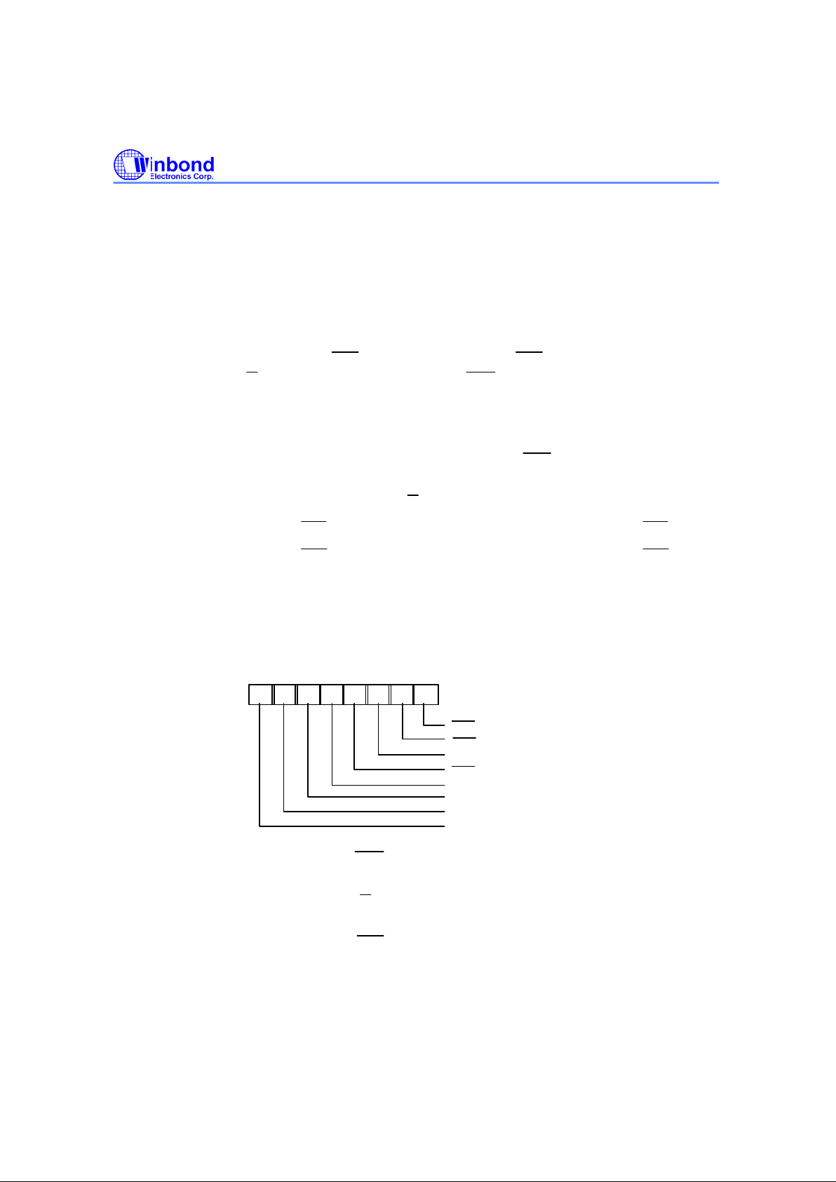
W83697SF
PRELIMINARY
Publication Release Date: April 2001
- 53 - Revision 0.51
Bit 4
When this bit is set to a logical 1, the UART enters diagnostic mode by an internal
loopback, as follows:
(1) SOUT is forced to logical 1, and SIN is isolated from the communication
link instead of
the TSR.
(2) Modem output pins are set to their inactive state.
(3) Modem input pins are isolated from the communication link and connect internally as
DTR (bit 0 of HCR) →
DSR
, RTS ( bit 1 of HCR) →
CTS
, Loopback RI input ( bit 2 of
HCR) →RI and IRQ enable ( bit 3 of HCR) →
DCD
.
Aside from the above connections, the UART operates normally. This method allows the
CPU to test the UART in a convenient way.
Bit 3 The UART interrupt output is enabled by setting this bit to a logic 1. In the diagnosti
c mode
this bit is internally connected to the modem control input DCD .
Bit 2
This bit is used only in the diagnostic mode. In the diagnostic mode this bit is internally
connected to the modem control input RI .
Bit 1
This bit controls the RTS output. The value of this bit is inverted and output to RTS .
Bit 0
This bit controls the DTR output. The value of this bit is inverted and output to DTR .
4.2.4 Handshake Status Register (HSR) (Read/Write)
This register reflects the current state of four input pins for handshake peripherals such as a modem and
records changes on these pins.
1234567 0
RI falling edge (FERI)
Clear to send (CTS)
Data set ready (DSR)
Ring indicator (RI)
Data carrier detect (DCD)
CTS
toggling (TCTS)
DSR
toggling (TDSR)
DCD
toggling (TDCD)
Bit 7
This bit is the opposite of the
DCD
input. This bit is equivalent to bit 3 of HCR in loopback
mode.
Bit 6
This bit is the opposite of the RI input. This bit
is equivalent to bit 2 of HCR in loopback
mode.
Bit 5
This bit is the opposite of the
DSR
input. This bit is equivalent to bit 0 of HCR in loopback
mode.
Page 59
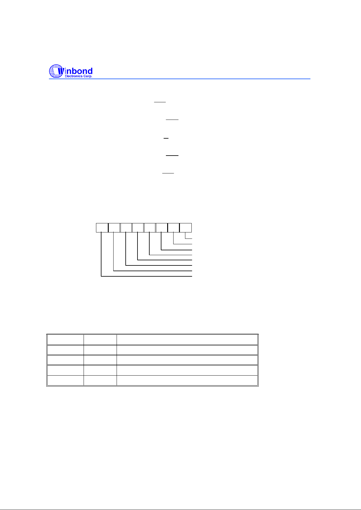
W83697SF
PRELIMINARY
Publication Release Date: April 2001
- 54 - Revision 0.51
Bit 4
This bit is the opposite of the
CTS
input. This bit is equivalent to bit 1 of HCR in loopback
mode.
Bit 3
TDCD. This bit indicates that the
DCD
pin has changed state after HSR was read by the
CPU.
Bit 2
FERI. This bit indicates that the RI
pin has changed from low to high state after HSR was
read by the CPU.
Bit 1
TDSR. This bit indicates that the
DSR
pin has changed state after HSR was read by the
CPU.
Bit 0
TCTS. This bit indicates that the
CTS
pin has changed state after HSR was read.
4.2.5 UART FIFO Control Register (SFR) (Write only)
This register is used to control the FIFO functions of the UART.
1234567 0
FIFO enable
Receiver FIFO reset
Transmitter FIFO reset
DMA mode select
Reserved
Reserved
RX interrupt active level (LSB)
RX interrupt active level (MSB)
Bit 6, 7
These two bits are used to set the active level for the receiver FIFO interrupt. For
example, if the interrupt active level is set as 4 bytes, once there are more than 4 data
characters in the receiver FIFO, the interrupt will be activated to notify the CPU to read
the data from the FIFO.
TABLE 4-3 FIFO TRIGGER LEVEL
BIT 7 BIT 6 RX FIFO INTERRUPT ACTIVE LEVEL (BYTES)
0 0 01
0 1 04
1 0 08
1 1 14
Bit 4, 5 Reserved
Bit 3 When this bit is programmed to logic 1, the DMA mode will change from mode 0 to mode 1
if SFR bit 0 = 1.
Page 60
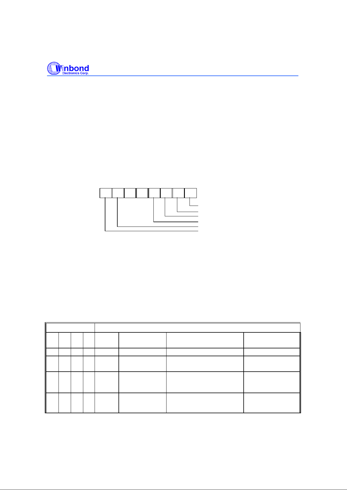
W83697SF
PRELIMINARY
Publication Release Date: April 2001
- 55 - Revision 0.51
Bit 2
Setting this bit to a logical 1 resets the TX FIFO counter logic to initial state. This bit will
clear to a logical 0 by itself after being set to a logical 1.
Bit 1 Setting this bit to a log
ical 1 resets the RX FIFO counter logic to initial state. This bit will
clear to a logical 0 by itself after being set to a logical 1.
Bit 0
This bit enables the 16550 (FIFO) mode of the UART. This bit should be set to a logical 1
before other bits of SF R are programmed.
4.2.6 Interrupt Status Register (ISR) (Read only)
This register reflects the UART interrupt status, which is encoded by different interrupt sources into 3
bits.
1234567
0
0 if interrupt pending
Interrupt Status bit 0
Interrupt Status bit 1
Interrupt Status bit 2
FIFOs enabled
FIFOs enabled
0 0
Bit 7, 6 These two bits are set to a logical 1 when SFR bit 0 = 1.
Bit 5, 4 These two bits are always logic 0.
Bit 3
In 16450 mode, this bit is 0. In 16550 mode, both bit 3 and 2 are set to a logical 1 when a
time-out interrupt is pending.
Bit 2, 1 These two bits identify the priority level of the pending interrupt, as
shown in the table
below.
Bit 0
This bit is a logical 1 if there is no interrupt pending. If one of the interrupt sources has
occurred, this bit will be set to a logical 0.
TABLE 4-4 INTERRUPT CONTROL FUNCTION
ISR INTERRUPT SET AND FU NCTION
Bit 3 Bit 2 Bit 1 Bit 0 Interrupt
priority
Interrupt Type
Interrupt Source
Clear Interrupt
0 0 0
1
- - No Interrupt pending -
0 1 1 0 First UART Receive
Status
1. OER = 1 2. PBER =1
3. NSER = 1 4. SBD = 1
Read USR
0 1 0 0 Second RBR Data Ready 1. RBR data ready
2. FIFO interrupt active level
reached
1. Read RBR
2. Read RBR until FIFO
data under active level
1 1 0 0 Second FIFO Data Timeout Data present in RX FIFO for 4
characters period of time since
last access of RX FIFO.
Read RBR
Page 61

W83697SF
PRELIMINARY
Publication Release Date: April 2001
- 56 - Revision 0.51
0 0 1 0 Third TBR Empty TBR empty 1. Write data into TBR
2. Read ISR (if priority is
third)
0 0 0 0 Fourth Handshake status 1. TCTS = 1 2. TDSR = 1
3. FERI = 1 4. TDCD = 1
Read HSR
** Bit 3 of ISR is enabled when bit 0 of SFR is logical 1.
Page 62
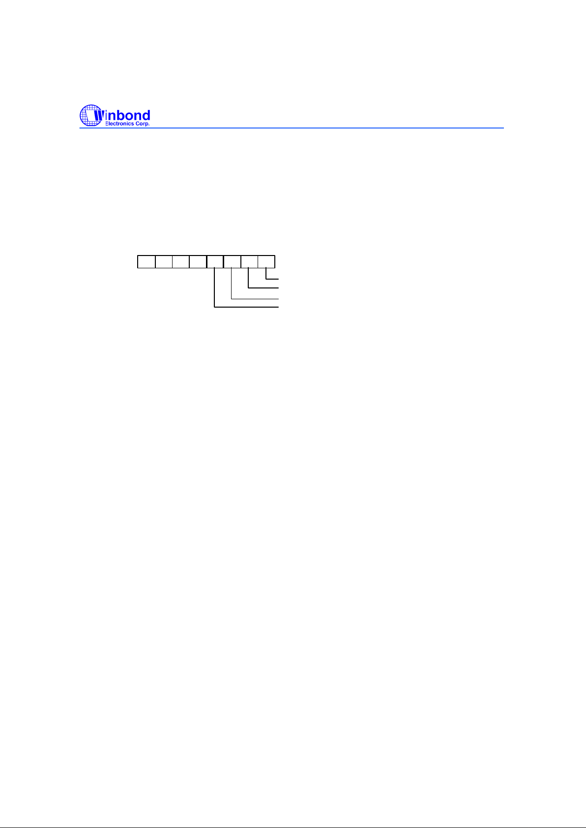
W83697SF
PRELIMINARY
Publication Release Date: April 2001
- 57 - Revision 0.51
4.2.7 Interrupt Control Register (ICR) (Read/Write)
This 8-bit register allows the five types of controller interrupts to activate the interrupt output signal
separately. The interrupt system can be totally disabled by resetting bits 0 through 3 of the Interrupt
Control Register (ICR). A selected interrupt can be enabled by setting the appropriate bits of this
register to a logical 1.
0 0 0
1234
5
67 0
0
RBR data ready interrupt enable (ERDRI)
TBR empty interrupt enable (ETBREI)
UART receive status interrupt enable (EUSRI)
Handshake status interrupt enable (EHSRI)
Bit 7-4: These four bits are always logic 0.
Bit 3 EHSRI. Setting this bit to a logical 1 enables the handshake status register interrupt.
Bit 2 EUSRI. Setting this bit to a logical 1 enables the UART status register interrupt.
Bit 1 ETBREI. Setting this bit to a logical 1 enables the TBR empty interrupt.
Bit 0: ERDRI. Setting this bit to a logical 1 enables the RBR data ready interrupt.
4.2.8 Programmable Baud Generator (BLL/BHL) (Read/Write)
Two 8-bit registers, BLL and BHL, compose a programmable baud generator that uses 24 MHz to
generate a 1.8461 MHz frequency and divides it by a divisor from 1 to 216-1. The output frequency of the
baud generator is the baud rate multiplied by 16, and this is the base frequency for the transmitter and
receiver. The table in the next page illustrates the use of the baud generator with a frequency of 1.8461
MHz. In high-speed UART mode (refer to CR0C bit7 and CR0C bit6), the programmable baud generator
directly uses 24 MHz and the same divisor as the normal speed divisor. In high-speed mode, the data
transmission rate can be as high as 1.5M bps.
Page 63

W83697SF
PRELIMINARY
Publication Release Date: April 2001
- 58 - Revision 0.51
4.2.9 User-defined Register (UDR) (Read/Write)
This is a temporary register that can be accessed and defined by the user.
TABLE 4-5 BAUD RATE TABLE
BAUD RATE FROM DIFFERENT PRE -DIVIDER
Pre-Div: 13
1.8461M Hz
Pre- Div:1.625
14.769M Hz
Pre-Div: 1.0
24M Hz
Decimal divisor used
to generate 16X clock
Error Percentage between
desired and actual
50 400 650 2304 **
75 600 975 1536 **
110 880 1430 1047 0.18%
134.5 1076 1478.5 857 0.099%
150 1200 1950 768 **
300 2400 3900 384 **
600 4800 7800 192 **
1200 9600 15600 96 **
1800 14400 23400 64 **
2000 16000 26000 58 0.53%
2400 19200 31200 48 **
3600 28800 46800 32 **
4800 38400 62400 24 **
7200 57600 93600 16 **
9600 76800 124800 12 **
19200 153600 249600 6 **
38400 307200 499200 3 **
57600 460800 748800 2 **
115200 921600 1497600 1 **
** The percentage error for all baud rates, except where indicated otherwise, is 0.16%.
Note. Pre-Divisor is determined by CRF0 of UART A and B.
Page 64
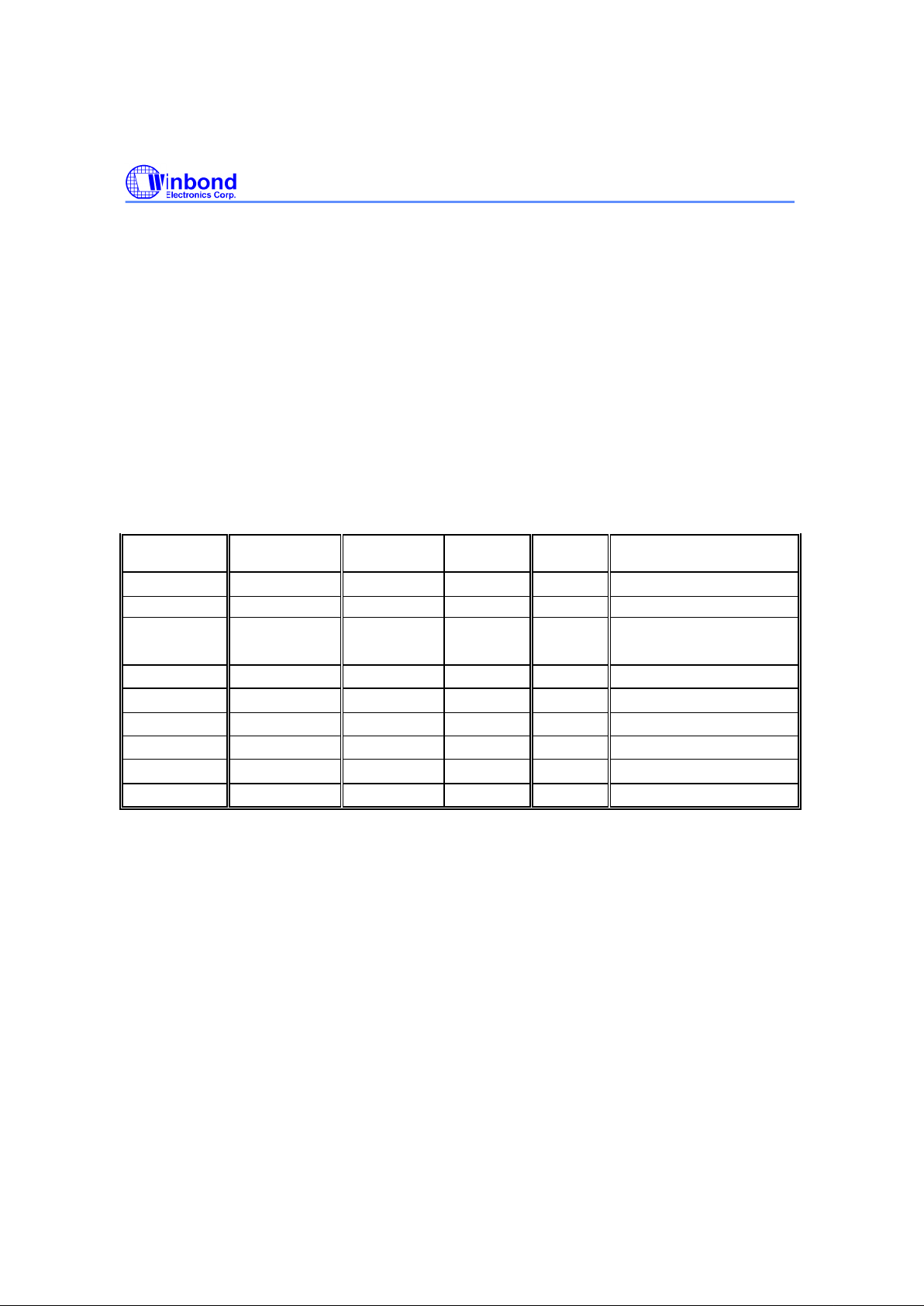
W83697SF
PRELIMINARY
Publication Release Date: April 2001
- 59 - Revision 0.51
5.0 PARALLEL PORT
5.1 Printer Interface Logic
The parallel port of the W83627SF makes possible the attachment of various devices that accept eight
bits of parallel data at standard TTL level. The W83627SF supports an IBM XT/AT compatible parallel
port (SPP), bi-directional parallel port (BPP), Enhanced Parallel Port (EPP), Extended Capabilities
Parallel Port (ECP), Extension FDD mode (EXTFDD), Extension 2FDD mode (EXT2FDD) on the parallel
port. Refer to the configuration registers for more information on disabling, power-down, and on selecting
the mode of operation.
Table 6-1 shows the pin definitions for different modes of the parallel port.
TABLE 6-1-1 PARALLEL PORT CONNECTOR AND PIN DEFINITIONS
HOST
CONNECTOR
PIN NUMBER
OF W83627SF
PIN
ATTRIBUTE
SPP EPP ECP
1 36 O nSTB nWrite
nSTB, HostClk
2
2-9 31 -26, 24-23 I/O PD<0:7> PD<0:7> PD<0:7>
10 22 I nACK Intr
nACK, PeriphClk2
11 21 I BUSY nWait
BUSY, PeriphAck2
12 19 I PE PE
PEerror, nAckReverse2
13 18 I SLCT Select
SLCT, Xflag2
14 35 O nAFD nDStrb
nAFD, HostAck2
15 34 I nERR nError
nFault1, nPeriphRequest2
16 33 O nINIT nInit
nINIT1, nReverseRqst2
17 32 O nSLIN nAStrb
nSLIN1 , ECPMode2
Notes:
n<name > : Active Low
1. Compatible Mode
2. High Speed Mode
3. For more information, refer to the IEEE 1284 standard.
Page 65
W83697SF
PRELIMINARY
Publication Release Date: April 2001
- 60 - Revision 0.51
TABLE 6-1-2 PARALLEL PORT CONNECTOR AND PIN DEFINITIONS
HOST
CONNECTOR
PIN NUMBER OF
W83627SF
PIN
ATTRIBUTE
SPP PIN
ATTRIBUTE
EXT2FDD PIN
ATTRIBUTE
EXTFDD
1 36 O nSTB --- --- --- --2 31 I/O PD0 I INDEX2#
I INDEX2#
3 30 I/O PD1 I TRAK02#
I TRAK02#
4 29 I/O PD2 I WP2#
I WP2#
5 28 I/O PD3 I RDATA2#
I RDATA2#
6 27 I/O PD4 I DSKCHG2#
I DSKCHG2#
7 26 I/O PD5 --- --- --- --8 24 I/O PD6 OD MOA2#
--- ---
9 23 I/O PD7 OD DSA2#
--- ---
10 22 I nACK OD DSB2#
OD DSB2#
11 21 I BUSY OD MOB2#
OD MOB2#
12 19 I PE OD WD2#
OD WD2#
13 18 I SLCT OD WE2#
OD WE2#
14 35 O nAFD OD RWC2#
OD RWC2#
15 34 I nERR OD HEAD2#
OD HEAD2#
16 33 O nINIT OD DIR2#
OD DIR2#
17 32 O nSLIN OD STEP2#
OD STEP2#
5.2 Enhanced Parallel Port (EPP)
TABLE 6-2 PRINTER MODE AND EPP REGISTER ADDRESS
A2 A1 A0 REGISTER NOTE
0 0 0 Data port (R/W) 1
0 0 1 Printer status bSFfer (Read) 1
0 1 0 Printer control latch (Write) 1
0 1 0 Printer control swapper (Read) 1
0 1 1 EPP address port (R/W) 2
1 0 0 EPP data port 0 (R/W) 2
1 0 1 EPP data port 1 (R/W) 2
1 1 0 EPP data port 2 (R/W) 2
1 1 1 EPP data port 2 (R/W) 2
Notes:
1. These registers are available in all modes.
2. These registers are available only in EPP mode.
Page 66

W83697SF
PRELIMINARY
Publication Release Date: April 2001
- 61 - Revision 0.51
Page 67
W83697SF
PRELIMINARY
Publication Release Date: April 2001
- 62 - Revision 0.51
5.2.1 Data Swapper
The system microprocessor can read the contents of the printer's data latch by reading the data
swapper.
5.2.2 Printer Status BSFfer
The system microprocessor can read the printer status by reading the address of the printer status
bSFfer. The bit definitions are as follows:
1
1 1
2354670
TMOUT
ERROR
SLCT
PE
BUSY
ACK
Bit 7 This signal is active during data entry, when the printer is off-line during printing, when the
print head is changing position, or during an error state. When this signal is active, the
printer is busy and cannot accept data.
Bit 6
This bit represents the current state of the printer's ACK# signal. A 0 means the printer
has received
a character and is ready to accept another. Normally, this signal will be active
for approximately 5 microseconds before BUSY# stops.
Bit 5 Logical 1 means the printer has detected the end of paper.
Bit 4 Logical 1 means the printer is selected.
Bit 3 Logical 0 means the printer has encountered an error condition.
Bit 1, 2 These two bits are not implemented and are logic one during a read of the status register.
Bit 0 This bit is valid in EPP mode only. It indicates that a 10 µS time-out has occu
rred on the
EPP bus. A logic 0 means that no time-
out error has occurred; a logic 1 means that a
time-out error has been detected. Writing a logic 1 to this bit will clear the time-
out status
bit; writing a logic 0 has no effect.
5.2.3 Printer Control Latch and Printer Control Swapper
The system microprocessor can read the contents of the printer control latch by reading the printer
control swapper. Bit definitions are as follows:
Page 68
W83697SF
PRELIMINARY
Publication Release Date: April 2001
- 63 - Revision 0.51
111
234567 0
STROBE
AUTO FD
SLCT IN
IRQ ENABLE
DIR
INIT
Bit 7, 6 These two bits are a logic one during a read. They can be written.
Bit 5 Direction control bit.
When this bit is a logic 1, the parallel port is in input mode (read); when it is a logic 0, the
parallel port is in output mode (write). This bit can be read and written. In SPP mode, this
bit is invalid and fixed at zero.
Bit 4
A 1 in this position allows an interrupt to occur when ACK# changes from low to high.
Bit 3 A 1 in this bit position selects the printer.
Bit 2 A 0 starts the printer (50 microsecond pulse, minimum).
Bit 1 A 1 causes the printer to line-feed after a line is printed.
Bit 0
A 0.5 microsecond minimum high active pulse clocks data into the printer. Valid data must
be present for a minimum of 0.5 microseconds before and after the strobe pulse.
5.2.4 EPP Address Port
The address port is available only in EPP mode. Bit definitions are as follows:
1
234
56
7 0
BC (Bad Cylinder)
MD (Missing Address Mark in Data Field).
1 If the FDC cannot find a data address mark
(or the address mark has been deleted)
when reading data from the media
0 No error
1 Bad Cylinder
0 No error
SN (Scan Not satisfied)
1 During execution of the Scan command
0 No error
SH (Scan Equal Hit)
1 During execution of the Scan command, if the equal condition is satisfied
0 No error
WC (Wrong Cylinder)
1 Indicates wrong Cylinder
DD (Data error in the Data field)
1 If the FDC detects a CRC error in the data field
0 No error
CM (Control Mark)
1 During execution of the read data or scan command
0 No error
Not used. This bit is always 0
Page 69
W83697SF
PRELIMINARY
Publication Release Date: April 2001
- 64 - Revision 0.51
The contents of DB0-DB7 are bSFfered (non-inverting) and output to ports PD0-PD7 during a write
operation. The leading edge of IOW# causes an EPP address write cycle to be performed, and the
trailing edge of IOW# latches the data for the duration of the EPP write cycle.
PD0-PD7 ports are read during a read operation. The leading edge of IOR# causes an EPP address read
cycle to be performed and the data to be output to the host CPU.
5.2.5 EPP Data Port 0-3
These four registers are available only in EPP mode. Bit definitions of each data port are as follows:
123456
7
0
PD0
PD1
PD2
PD3
PD4
PD5
PD6
PD7
When accesses are made to any EPP data port, the contents of DB0 -DB7 are bSFfered (non-inverting)
and output to the ports PD0-PD7 during a write operation. The leading edge of IOW# causes an EPP
data write cycle to be performed, and the trailing edge of IOW# latches the data for the duration of the
EPP write cycle.
During a read operation, ports PD0-PD7 are read, and the leading edge of IOR# causes an EPP read
cycle to be performed and the data to be output to the host CPU.
5.2.6 Bit Map of Parallel Port and EPP Registers
REGISTER
7 6 5 4 3 2 1 0
Data Port (R/W)
PD7 PD6 PD5 PD4 PD3 PD2 PD1 PD0
Status BSFfer (Read)
BUSY# ACK# PE SLCT
ERROF#
1 1 TMOUT
Control Swapper
(Read)
1 1 1 IRQEN SLIN INIT# AUTOFD# STROBE#
Control Latch (Write)
1 1 DIR IRQ SLIN INIT# AUTOFD# STROBE#
EPP Address Port R/W)
PD7 PD6 PD5 PD4 PD3 PD2 PD1 PD0
EPP Data Port 0 (R/W)
PD7 PD6 PD5 PD4 PD3 PD2 PD1 PD0
E PP Data Port 1 (R/W)
PD7 PD6 PD5 PD4 PD3 PD2 PD1 PD0
EPP Data Port 2 (R/W)
PD7 PD6 PD5 PD4 PD3 PD2 PD1 PD0
Page 70

W83697SF
PRELIMINARY
Publication Release Date: April 2001
- 65 - Revision 0.51
EPP Data Port 3 (R/W)
PD7 PD6 PD5 PD4 PD3 PD2 PD1 PD0
Page 71
W83697SF
PRELIMINARY
Publication Release Date: April 2001
- 66 - Revision 0.51
5.2.7 EPP Pin Descriptions
EPP NAME TYPE EPP DESCRIPTION
nWrite O Denotes an address or data read or write operation.
PD<0:7> I/O Bi-directional EPP address and data bus.
Intr I Used by peripheral device to interrupt the host.
nWait I Inactive to acknowledge that data transfer is completed. Active to indicate
that the device is ready for the next transfer.
PE I Paper end; same as SPP mode.
Select I Printer selected status; same as SPP mode.
nDStrb O This signal is active low. It denotes a data read or write operation.
nError I Error; same as SPP mode.
nInits O This signal is active low. When it is active, the EPP device is reset to its
initial operating mode.
nAStrb O This signal is active low. It denotes an address read or write operation.
5.2.8 EPP Operation
When the EPP mode is selected in the configuration register, the standard and bi -directional modes are
also available. The PDx bus is in the standard or bi-directional mode when no EPP read, write, or
address cycle is currently being executed. In this condition all output signals are set by the SPP Control
Port and the direc tion is controlled by DIR of the Control Port.
A watchdog timer is required to prevent system lockup. The timer indicates that more than 10 µS have
elapsed from the start of the EPP cycle to the time
WAIT#
is deasserted. The current EPP cycle is
aborted when a time -out occurs. The time-out condition is indicated in Status bit 0.
5.2.8.1 EPP Operation
The EPP operates on a two-phase cycle. First, the host selects the register within the device for
subsequent operations. Second, the host performs a series of read and/or write byte operations to the
selected register. Four operations are supported on the EPP: Address Write, Data Write, Address Read,
and Data Read. All operations on the EPP device are performed asynchronously.
5.2.8.2 EPP Version 1.9 Operation
The EPP read/write operation can be completed under the following conditions:
a. If the nWait is active low, when the read cycle (nWrite inactive high, nDStrb/nAStrb active low) or write
cycle (nWrite active low, nDStrb/nAStrb active low) starts, the read/write cycle proceeds normally
and will be completed when nWait goes inactive high.
b. If nWait is inactive high, the read/write cycle will not start. It must wait until nWait changes to active
low, at which time it will start as described above.
5.2.8.3 EPP Version 1.7 Operation
Page 72

W83697SF
PRELIMINARY
Publication Release Date: April 2001
- 67 - Revision 0.51
The EPP read/write cycle can start without checking whether nWait is active or inactive. Once the
read/write cycle starts, however, it will not terminate until nWait changes from active low to inactive high.
Page 73
W83697SF
PRELIMINARY
Publication Release Date: April 2001
- 68 - Revision 0.51
5.3 Extended Capabilities Parallel (ECP) Port
This port is software and hardware compatible with existing parallel ports, so it may be used as a
standard printer mode if ECP is not required. It provides an automatic high burst-bandwidth channel that
supports DMA for ECP in both the forward (host to peripheral) and reverse (peripheral to host) directions.
Small FIFOs are used in both forward and reverse directions to improve the maximum bandwidth
requirement. The size of the FIFO is 16 bytes. The ECP port supports an automa tic handshake for the
standard parallel port to improve compatibility mode transfer speed.
The ECP port supports run-length-encoded (RLE) decompression (required) in hardware. Compression is
accomplished by counting identical bytes and transmitting an RLE byte that indicates how many times
the next byte is to be repeated. Hardware support for compression is optional.
For more information about the ECP Protocol, refer to the Extended Capabilities Port Protocol and ISA
Interface Standard.
5.3.1 ECP Register and Mode Definitions
NAME ADDRESS I/O ECP MODES FUNCTION
data Base+000h R/W 000-001 Data Register
ecpAFifo Base+000h R/W 011 ECP FIFO (Address)
dsr Base+001h R All Status Register
dcr Base+002h R/W All Control Register
cFifo Base+400h R/W 010 Parallel Port Data FIFO
ecpDFifo Base+400h R/W 011 ECP FIFO (DATA)
tFifo Base+400h R/W 110 Test FIFO
cnfgA Base+400h R 111 Configuration Register A
cnfgB Base+401h R/W 111 Configuration Register B
ecr Base+402h R/W All Extended Control Register
Note: The base addresses are specified by CR23, which are determined by configuration register or hardware setting.
MODE DESCRIPTION
000 SPP mode
001 PS/2 Parallel Port mode
010 Parallel Port Data FIFO mode
011 ECP Parallel Port mode
100 EPP mode (If this option is enabled in the CR9 and CR0 to select ECP/EPP mode)
101 Reserved
110 Test mode
111 Configuration mode
Note: The mode selection bits are bit 7-5 of the Extended Control Register.
Page 74
W83697SF
PRELIMINARY
Publication Release Date: April 2001
- 69 - Revision 0.51
5.3.2 Data and ecpAFifo Port
Modes 000 (SPP) and 001 (PS/2) (Data Port)
During a write operation, the Data Register latches the contents of the data bus on the rising edge of the
input. The contents of this register are output to the PD0-PD7 ports. During a read operation, ports PD0PD7 are read and output to the host. The bit definitions are as follows:
7 6 5 4 3 2 1 0
PD0
PD1
PD2
PD3
PD4
PD5
PD6
PD7
Mode 011 (ECP FIFO- Address/RLE)
A data byte written to this address is placed in the FIFO and tagged as an ECP Address/RLE. The
hardware at the ECP port transmits this byte to the peripheral automatically. The operation of this
register is defined only for the forward direction. The bit definitions are as follows:
7 6 5 4 3 2 1 0
Address or RLE
Address/RLE
5.3.3 Device Status Register (DSR)
These bits are at low level during a read of the Printer Status Register. The bits of this status register are
defined as follows:
7 6 5 4 3 2 1 0
nFault
Select
PError
nAck
nBusy
11 1
Page 75
W83697SF
PRELIMINARY
Publication Release Date: April 2001
- 70 - Revision 0.51
Bit 7 This bit reflects the complement of the Busy input.
Bit 6 This bit reflects the nAck input.
Bit 5 This bit reflects the PError input.
Bit 4 This bit reflects the Select input.
Bit 3 This bit reflects the nFault input.
Bit 2-0 These three bits are not implemented and are always logic one during a read.
5.3.4 Device Control Register (DCR)
The bit definitions are as follows:
7 6 5 4 3 2 1 0
VCOREA
VCOREB
+3.3VIN
+5VIN
TEMP1
TEMP2
FAN1
FAN2
Bit 6, 7 These two bits are logic one during a read and cannot be written.
Bit 5 This bit has
no effect and the direction is always out if mode = 000 or mode = 010.
Direction is valid in all other modes.
0 the parallel port is in output mode.
1 the parallel port is in input mode.
Bit 4 Interrupt request enable. When this bit is set to a hi
gh level, it may be used to enable
interrupt requests from the parallel port to the CPU due to a low to high transition on the
ACK#
input.
Bit 3 This bit is inverted and output to the
SLIN#
output.
0 The printer is not selected.
1 The printer is selected.
Bit 2 This bit is output to the
INIT#
output.
Bit 1 This bit is inverted and output to the
AFD#
output.
Bit 0 This bit is inverted and output to the STB# output.
Page 76

W83697SF
PRELIMINARY
Publication Release Date: April 2001
- 71 - Revision 0.51
5.3.5 cFifo (Parallel Port Data FIFO) Mode = 010
This mode is defined only for the forward direction. The standard parallel port protocol is used by a
hardware handshake to the peripheral to transmit bytes written or DMAed from the system to this FIFO.
Transfers to the FIFO are byte aligned.
5.3.6 ecpDFifo (ECP Data FIFO) Mode = 011
When the direction bit is 0, bytes written or DMAed from the system to this FIFO are transmitted by a
hardware handshake to the peripheral using the ECP parallel port protocol. Transfers to the FIFO are
byte aligned.
When the direction bit is 1, data bytes from the peripheral are read under automatic hardware handshake
from ECP into this FIFO. Reads or DMAs from the FIFO will return bytes of ECP data to the system.
5.3.7 tFifo (Test FIFO Mode) Mode = 110
Data bytes may be read, written, or DMAed to or from the system to this FIFO in any direction. Data in
the tFIFO will not be transmitted to the parallel port lines. However, data in the tFIFO may be displayed
on the parallel port data lines.
5.3.8 cnfgA (Configuration Register A) Mode = 111
This register is a read- only register. When it is read, 10H is returned. This indicates to the system that
this is an 8-bit implementation.
5.3.9 cnfgB (Configuration Register B) Mode = 111
The bit definitions are as follows:
7 6 5 4 3 2 1 0
1 1 1
intrValue
compress
IRQx 0
IRQx 1
IRQx 2
Bit 7 This bit is read-only
. It is at low level during a read. This means that this chip does not
support hardware RLE compression.
Bit 6 Returns the value on the ISA IRQ line to determine possible conflicts.
Bit 5-3 Reflect the IRQ resource assigned for ECP port.
Page 77
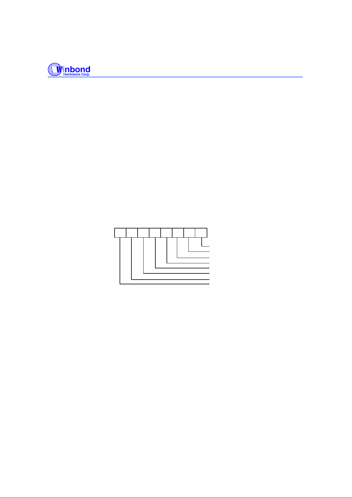
W83697SF
PRELIMINARY
Publication Release Date: April 2001
- 72 - Revision 0.51
cnfgB[5:3] IRQ resource
000 reflect other IRQ resources selected by PnP register (default)
001 IRQ7
010 IRQ9
011 IRQ10
100 IRQ11
101 IRQ14
110 IRQ15
111 IRQ5
Bit 2-0
These five bits are at high level during a read and can be written.
5.3.10 ecr (Extended Control Register) Mode = all
This register controls the extended ECP parallel port functions. The bit definitions are follows:
7 6 5 4 3 2 1 0
empty
full
service Intr
dmaEn
nErrIntrEn
MODE
MODE
MODE
Bit 7- 5: These bits are read/write and select the mode.
000 Standard Parallel Port mode. The FIFO is res et in this mode.
001 PS/2 Parallel Port mode. This is the same as 000 except that direction may be used
to tri-state the data lines and reading the data register returns the value on the data
lines and not the value in the data register.
010 Parallel Port FIFO mode. This is the same as 000 except that bytes are written or
DMAed to the FIFO. FIFO data are automatically transmitted using the standard
parallel port protocol. This mode is useful only when direction is 0.
011 ECP Parallel Port Mode. When the direction is 0 (forward direction), bytes placed into
the ecpDFifo and bytes written to the ecpAFifo are placed in a single FIFO and auto
transmitted to the peripheral using ECP Protocol. When the direction is 1 (reverse
direction), bytes are moved from the ECP parallel port and packed into bytes in the
ecpDFifo.
100 Selects EPP Mode. In this mode, EPP is activated if the EPP mode is selected.
101 Reserved.
110 Test Mode. The FIFO may be written and read in this mode, but the data will not be
transmitted on the parallel port.
Page 78
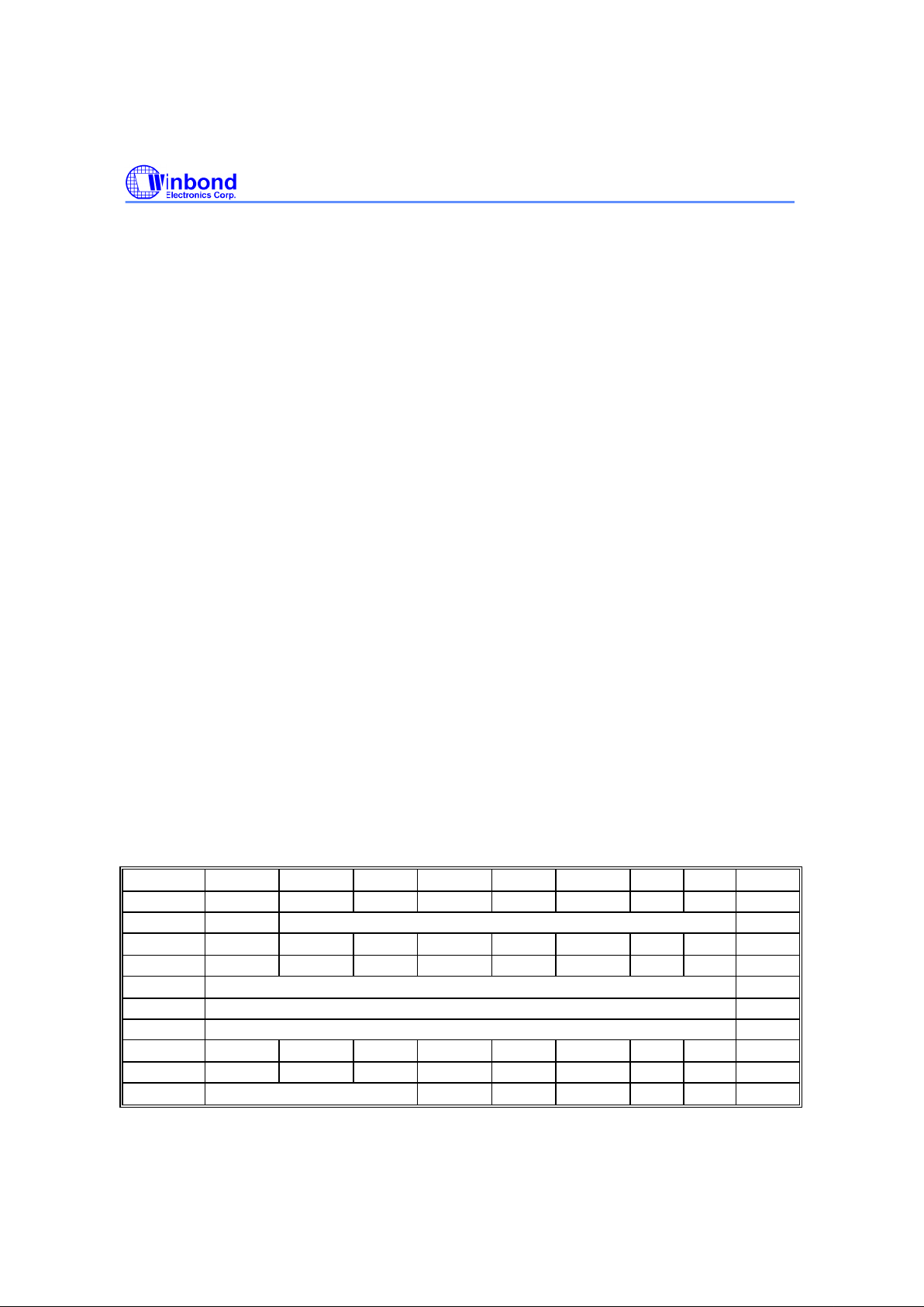
W83697SF
PRELIMINARY
Publication Release Date: April 2001
- 73 - Revision 0.51
111 Configuration Mode. The confgA and confgB registers are accessible at 0x400 and
0x401 in this mode.
Bit 4: Read/Write (Valid only in ECP Mode)
1 Disables the interrupt generated on the asserting edge of nFault.
0 Enables an interrupt pulse on the high to low edge of nFault. If nFault is asserted
(interrupt) an interrupt will be generated and this bit is written from a 1 to 0.
Bit 3: Read/Write
1 Enables DMA.
0 Disables DMA unconditionally.
Bit 2: Read/Write
1 Disables DMA and all of the service interrupts.
0 Enables one of the following cases of interrupts. When one of the service interrupts
has occurred, the serviceIntr bit is set to a 1 by hardware. This bit must be reset to 0
to re -enable the interrupts. Writing a 1 to this bit will not cause an interrupt.
(a) dmaEn = 1: During DMA this bit is set to a 1 when terminal count is reached.
(b) dmaEn = 0 direction = 0: This bit is set to 1 whenever there are writeIntr Threshold
or more bytes free in the FIFO.
(c) dmaEn = 0 direction = 1: This bit is set to 1 whenever there are readIntr Threshold
or more valid bytes to be read from the FIFO.
Bit 1: Read only
0 The FIFO has at least 1 free byte.
1 The FIFO cannot accept another byte or the FIFO is completely full.
Bit 0: Read only
0 The FIFO contains at least 1 byte of data.
1 The FIFO is completely empty.
5.3.11 Bit Map of ECP Port Registers
D7 D6 D5 D4 D3 D2 D1 D0 NOTE
data
PD7 PD6 PD5 PD4 PD3 PD2 PD1 PD0
ecpAFifo
Addr/RLE Address or RLE field 2
dsr
n Busy nAck PError Select nFault 1 1 1 1
dcr
1 1 Directio ackIntEn SelectIn nInit autofd strobe 1
cFifo
Parallel Port Data FIFO 2
ecpDFifo
ECP Data FIFO 2
tFifo
Test FIFO 2
cnfgA
0 0 0 1 0 0 0 0
cnfgB
compress intrValue 1 1 1 1 1 1
ecr
MODE nErrIntrEn dmaEn serviceIntr full empty
Page 79

W83697SF
PRELIMINARY
Publication Release Date: April 2001
- 74 - Revision 0.51
Notes:
1. These registers are available in all modes.
2. All FIFOs use one common 16-byte FIFO.
Page 80

W83697SF
PRELIMINARY
Publication Release Date: April 2001
- 75 - Revision 0.51
5.3.12 ECP Pin Descriptions
NAME TYPE DESCRIPTION
nStrobe (HostClk) O The nStrobe registers data or address into the slave on the
asserting edge during write operations. This signal handshakes
with Busy.
PD<7:0> I/O These signals contains address or data or RLE data.
nAck (PeriphClk) I This signal indicates valid data driven by the peripheral when
asserted. This signal hands hakes with nAutoFd in reverse.
Busy (PeriphAck) I This signal deasserts to indicate that the peripheral can accept
data. It indicates whether the data lines contain ECP command
information or data in the reverse direction. When in reverse
direction, norma l data are transferred when Busy (PeriphAck) is
high and an 8-bit command is transferred when it is low.
PError (nAckReverse) I This signal is used to acknowledge a change in the direction of
the transfer (asserted = forward). The peripheral drives this signal
low to acknowledge nReverseRequest. The host relies upon
nAckReverse to determine when it is permitted to drive the data
bus.
Select (Xflag) I Indicates printer on line.
nAutoFd (HostAck) O Requests a byte of data from the peripheral when it is asserted.
This signal indicates whether the data lines contain ECP address
or data in the forward direction. When in forward direction, normal
data are transferred when nAutoFd (HostAck) is high and an 8-bit
command is transferred when it is low.
nFault (nPeriphRequest)
I
Generates an error interrupt when it is asserted. This signal is
valid only in the forward direction. The peripheral is permitted (but
not required) to drive this pin low to request a reverse transfer
during ECP Mode.
nInit (nReverseRequest)
O
This signal sets the transfer direction (asserted = reverse,
deasserted = forward). This pin is driven low to place the channel
in the reverse direction.
nSelectIn (ECPMode)
O
This signal is always deasserted in ECP mode.
Page 81

W83697SF
PRELIMINARY
Publication Release Date: April 2001
- 76 - Revision 0.51
5.3.13 ECP Operation
The host must negotiate on the parallel port to determine if the peripheral supports the ECP protocol
before ECP operation. After negotiation, it is necessary to initialize some of the port bits. The following
are required:
(a) Set direction = 0, enabli ng the drivers.
(b) Set strobe = 0, causing the nStrobe signal to default to the deasserted state.
(c) Set autoFd = 0, causing the nAutoFd signal to default to the deasserted state.
(d) Set mode = 011 (ECP Mode)
ECP address/RLE bytes or data bytes may be sent automatically by writing the ecpAFifo or ecpDFifo,
respectively.
Mode Switching
Software will execute P1284 negotiation and all operation prior to a data transfer phase under
programmed I/O control (mode 000 or 001). Hardware provides an automatic control line handshake,
moving data between the FIFO and the ECP port only in the data transfer phase (mode 011 or 010).
If the port is in mode 000 or 001 it may switch to any other mode. If the port is not in mode 000 or 001 it
can only be switched into mode 000 or 001. The direction can be changed only in mode 001.
When in extended forward mode, the software should wait for the FIFO to be empty before switching
back to mode 000 or 001. In ECP reverse mode the software waits for all the data to be read from the
FIFO before changing back to mode 000 or 001.
Command/Data
ECP mode allows the transfer of normal 8-bit data or 8-bit commands. In the forward direction, normal
data are transferred when HostAck is high and an 8-bit command is transferred when HostAck is low.
The most significant bits of the command indicate whether it is a run-length count (for compression) or a
channel address.
In the reverse direction, normal data are transferred when PeriphAck is high and an 8- bit command is
transferred when PeriphAck is low. The most significant bit of the command is always zero.
Data Compression
The W83627SF supports run length encoded (RLE) decompression in hardware and can transfer
compressed data to a peripheral. Note that the odd (RLE) compression in hardware is not supported. In
order to transfer data in ECP mode, the compression count is written to the ecpAFifo and the data byte
is written to the ecpDFifo.
5.3.14 FIFO Operation
The FIFO threshold is set in configuration register 5. All data transfers to or from the parallel port can
proceed in DMA or Programmed I/O (non-DMA) mode, as indicated by the selected mode. The FIFO is
used by selecting the Parallel Port FIFO mode or ECP Parallel Port Mode. After a reset, the FIFO is
disabled.
Page 82

W83697SF
PRELIMINARY
Publication Release Date: April 2001
- 77 - Revision 0.51
5.3.15 DMA Transfers
DMA transfers are always to or from the ecpDFifo, tFifo, or CFifo. The DMA uses the standard PC DMA
services. The ECP requests DMA transfers from the host by activating the PDRQ pin. The DMA will
empty or fill the FIFO using the appropriate direction and mode. When the terminal count in the DMA
controller is reached, an interrupt is generated and serviceIntr is asserted, which will disable the DMA.
5.3.16 Programmed I/O (NON-DMA) Mode
The ECP or parallel port FIFOs can also be operated using interrupt driven programmed I/O.
Programmed I/O transfers are to the ecpDFifo at 400H and ecpAFifo at 000H or from the ecpDFifo
located at 400H, or to/from the tFifo at 400H. The host must set the direction, state, dmaEn = 0 and
serviceIntr = 0 in the programmed I/O transfers.
The ECP requests programmed I/O transfers from the host by activating the IRQ pin. The programmed
I/O will empty or fill the FIFO using the appropriate direction and mode.
5.4 Extension FDD Mode (EXTFDD)
In this mode, the W8 3627SF changes the printer interface pins to FDC input/output pins, allowing the
user to install a second floppy disk drive (FDD B) through the DB-25 printer connector. The pin
assignments for the FDC input/output pins are shown in Table 6-1.
After the printer interface is set to EXTFDD mode, the following occur:
(1) Pins
MOB#
and
DSB#
will be forced to inactive state.
(2) Pins
DSKCHG#
,
RDATA#, WP#, TRAK0#, INDEX#
will be logically ORed with pins PD4-PD0 to
serve as input signals to the FDC.
(3) Pins PD4-PD0 each will have an internal resistor of about 1K ohm to serve as pull-up resistor for FDD
open drain/collector output.
(4) If the parallel port is set to EXTFDD mode after the system has booted DOS or another operating
system, a warm reset is needed to enable the system to recognize the extension floppy drive.
5.5 Extension 2FDD Mode (EXT2FDD)
In this mode, the W83627SF changes the printer interface pins to FDC input/output pins, allowing the
user to install two external floppy disk drives through the DB -25 printer connector to replace internal
floppy disk drives A and B. The pin assignments for the FDC input/output pins are shown in Table6-1.
After the printer interface is set to EXTFDD mode, the following occur:
(1) Pins
MOA#, DSA#, MOB#
, and
DSB#
will be forced to inactive state.
(2) Pins
DSKCHG#, RDATA#, WP#, TRAK0#
, and
INDEX#
will be logically ORed with pins PD4 -PD0 to
serve as input signals to the FDC.
(3) Pins PD4-PD0 each will have an internal resistor of about 1K ohm to serve as pull-up res istor for FDD
open drain/collector output.
(4) If the parallel port is set to EXT2FDD mode after the system has booted DOS or another operating
system, a warm reset is needed to enable the system to recognize the extension floppy drive.
Page 83
W83697SF
PRELIMINARY
Publication Release Date: April 2001
- 78 - Revision 0.51
6.0 GENERAL PURPO SE I/O
W83697SF provides 60 input/output ports that can be individually configured to perform a simple basic
I/O function or a pre-defined alternate function. Those 60 GP I/O ports are divided into three groups,
each group contains 8 ports. The first gro up is configured through control registers in logical device 7,
the second group in logical device 8, and the third group in logical device 9. Users can configure each
individual port to be an input or output port by programming respective bit in selection register (CRF0: 0 =
output, 1 = input). Invert port value by setting inversion register (CRF2: 0 = non -inverse, 1 = inverse).
Port value is read/written through data register (CRF1). Table 7.1 and 7.2 gives more details on GPIO's
assignment. In addit ion, GPIO1 is designed to be functional even in power loss condition (VCC or VSB
is off). Figure 7.1 shows the GP I/O port's structure. Right after Power-on reset, those ports default to
perform basic input function except ports in GPIO1 which maintains its previous settings until a battery
loss condition.
Table 7.1
SELECTION BIT
0 = OUTPUT
1 = INPUT
INVERSION BIT
0 = NON INVERSE
1 = INVERSE
BASIC I/O OPERATIONS
0 0 Basic non -inverting output
0 1 Basic inverting output
1 0 Basic non -inverting input
1 1 Basic inverting input
Page 84
W83697SF
PRELIMINARY
Publication Release Date: April 2001
- 79 - Revision 0.51
Table 7.2
GP I/O PORT DATA REGISTER REGISTER BIT ASSIGNMENT GP I/O PORT
BIT 0 GP10
BIT 1 GP11
BIT 2 GP12
BIT 3 GP13
GP1 BIT 4 GP14
BIT 5 GP15
BIT 6 GP16
BIT 7 GP17
BIT 0 GP20
BIT 1 GP21
GP2 BIT 2 GP22
BIT 3 GP23
BIT 4 GP24
BIT 5 GP25
BIT 6 GP26
BIT 7 GP27
BIT 0 GP30
BIT 1 GP31
BIT 2 GP32
BIT 3 GP33
GP3 BIT 4 GP34
BIT 5 GP35
BIT 6 GP36
BIT 7 GP37
Page 85
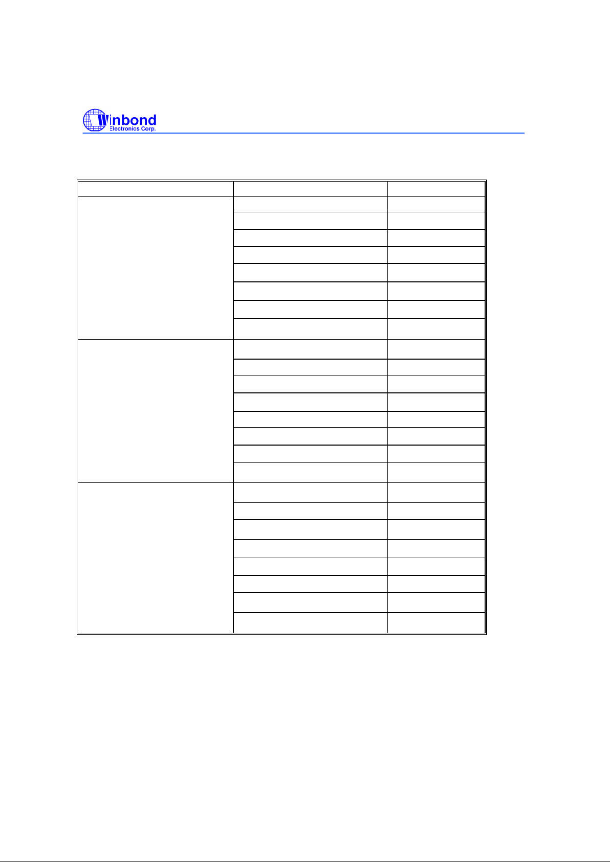
W83697SF
PRELIMINARY
Publication Release Date: April 2001
- 80 - Revision 0.51
Table 7.2, continued
GP I/O PORT DATA REGISTER REGISTER BIT ASSIGNMENT GP I/O PORT
BIT 0 GP40
BIT 1 GP41
BIT 2 GP42
BIT 3 GP43
GP4 BIT 4 GP44
BIT 5 GP45
BIT 6 GP46
BIT 7 GP47
BIT 0 GP50
BIT 1 GP51
BIT 2 GP52
GP5 BIT 3 GP53
BIT 4 GP54
BIT 5 GP55
BIT 6 GP56
BIT 7 GP57
BIT 0 GP60
BIT 1 GP61
BIT 2 GP62
BIT 3 GP63
GP6 BIT 4 GP64
BIT 5 GP65
BIT 6 GP66
BIT 7
GP67
Page 86
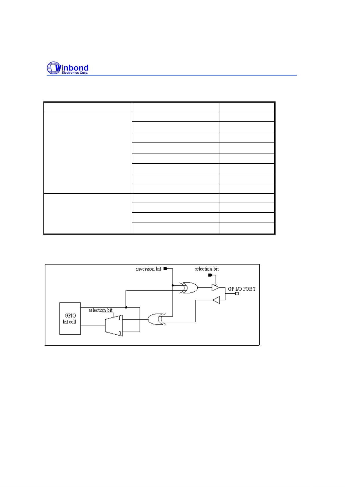
W83697SF
PRELIMINARY
Publication Release Date: April 2001
- 81 - Revision 0.51
Table 7.2, continued
GP I/O PORT DATA REGISTER REGISTER BIT ASSIGNMENT GP I/O PORT
BIT 0 GP70
BIT 1 GP71
BIT 2 GP72
GP7 BIT 3 GP73
BIT 4 GP74
BIT 5 GP75
BIT 6 GP76
BIT 7 GP77
BIT 0 GP80
GP8 BIT 1 GP81
BIT 2 GP82
BIT 3 GP83
Figure 7.1
Page 87
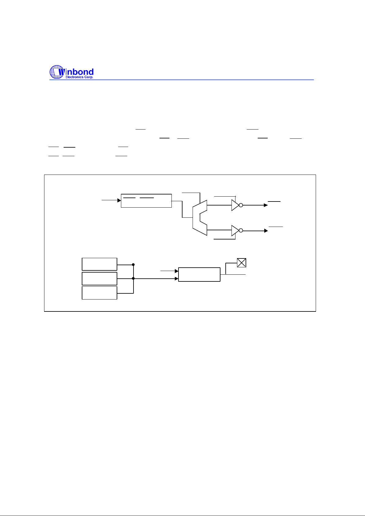
W83697SF
PRELIMINARY
Publication Release Date: April 2001
- 82 - Revision 0.51
7.0 ACPI REGISTERS FEATURES
W83697SF supports both ACPI and legacy power managements. The switch logic of the power
management block generates an SMI interrupt in the legacy mode and an PME interrupt in the ACPI
mode. The new ACPI feature routes
SMI/PME
logic output either to
SMI
or to
PME
.The
SMI/PME
logic routes to
SMI
only when both PME_EN = 0 and SMIPME_OE = 1. Similarly, the
SMI/PME logic routes to PME only when both PME_EN = 1 and SMIPME_OE = 1.
Device Idle
Timers
Device Trap
Timer
Sleep/Wake
State machine
WAK_STS
Clock
Control
PME
SMI
Global STBY
IRQs
Logic
IRQ events
PME_EN
SMIPME_OE
PMESMI /
0
1
SMIPME_OE
Page 88
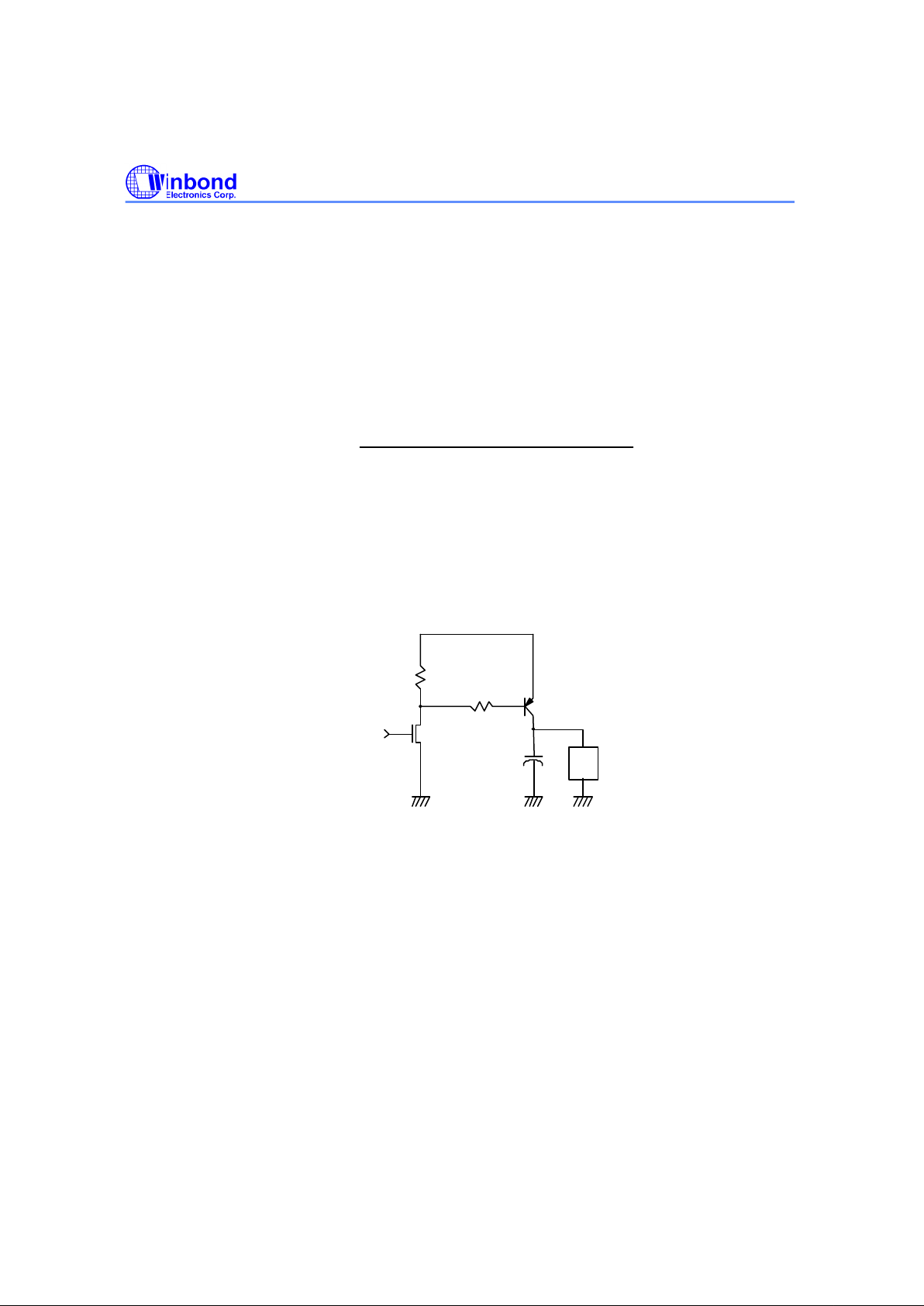
W83697SF
PRELIMINARY
Publication Release Date: April 2001
- 83 - Revision 0.51
8.0 PULSE WIDTH MODULATION (PWM)
8.1 General Description
The W83697SF provides 3 sets for fan PWM speed control. The duty cycle of PWM can be programmed
by the 8-bit registers which are defined in the CR01, CR03 and CR11. The default duty cycle is set to
100%, that is, the default 8-bit registers is set to FFh. the expression of duty can be represented as
follows.
%. 0 cycleduty the0, alueregister vbit -8 programmed If
0.alueregister vbit -8 Programmed
,%100
256
1 Valueer bit Regist-8 Programmed
(%)cycleDuty
==
≠
×
+
=−
The PWM clock frequency also can be program and defined in the CR00, CR02 and CR10. The
application circuit is shown as the Figure 9.1.
+12V
FAN
R1
R2
NMOS
PNP Transistor
C
+
-
PWM Clock Input
D
S
G
Figure 9.1 : The PWM application circuit
8.2 LPC Interface
The interface uses LPC Bus to access which the ports of low byte (bit2~bit0) are defined in the port 5h
and 6h. The other higher bits of these ports is set by W83697SF itself. The general decoded address is
set to port 295h and port 296h. These two ports are described as following:
Port 295h: Index port.
Port 296h: Data port.
Page 89
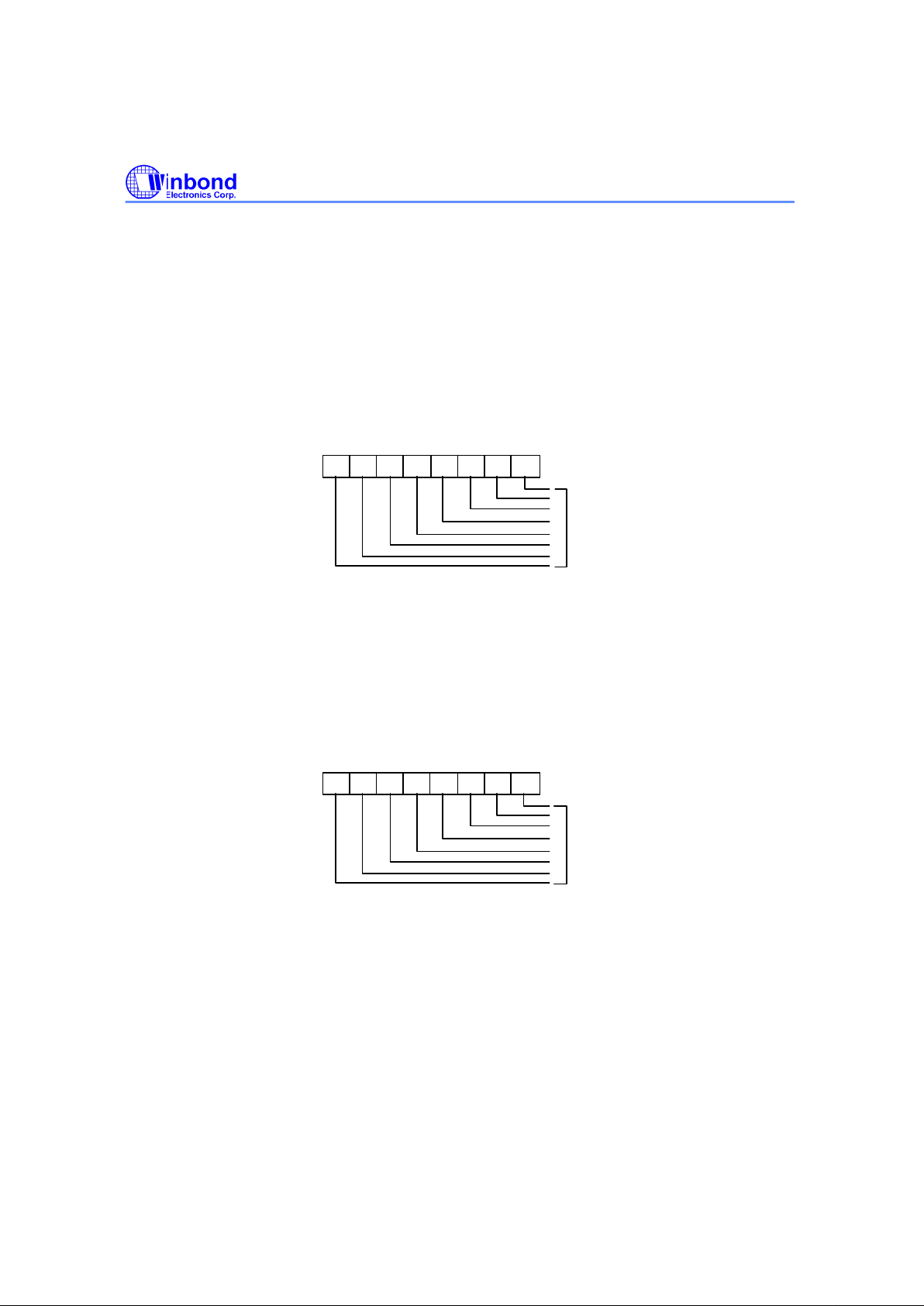
W83697SF
PRELIMINARY
Publication Release Date: April 2001
- 84 - Revision 0.51
8.3 REGISTERS
8.3.1 Address Register (Port x5h)
Data Port: Port x5h
Power on Default Value FFh
Attribute: Bit 7:0 Read/write
Size: 8 bits
7 6 5 4 3 2 1 0
Data
Bit 7- 0: Read/Write address pointer.
8.3.2 Data Register (Port x6h)
Data Port: Port x6h
Power on Default Value 00h
Attribute: Read/write
Size: 8 bits
7 6 5 4 3 2 1 0
Data
Bit 7- 0: Data to be read from or to be written to Register.
Page 90

W83697SF
PRELIMINARY
Publication Release Date: April 2001
- 85 - Revision 0.51
8.3.3 PWM 1 Pre -Scale Re gister -- Index 00h
Power on default [7:0] = 0000-0001 b
Bit Name Read/Write Description
7 PWM_CLK_SEL1 Read/Write PWM 1 Input Clock Select. This bit select PWM 1 input
clock to pre-scale divider.
0: 24 MHz
1: 187.5 KHz
6-0 PRE_SCALE1[6:0] Read/Write PWM 1 Input Clock Pre-Scale. The divider of input
clock is the number defined by pre-scale. Thus, writing 0
transfers the input clock directly to counter. The
maximum divider is 128 (7Fh).
00h : divider is 1
01h : divider is 2
02h : divider is 3
:
:
PWM 1 frequency = (Input Clock / Pre -scale) / 256
8.3.4 PWM 1 Duty Cycle Select Register – Index 01h
Power on default [7:0] 1111,1111 b
Bit Name Read/Write Description
7-0 PWM1_DC[7:0] Read/Write PWM 1 Duty Cycle. This 8-bit register determines the
number of the 256-cycle period.
00h: PWM output is always logical Low.
FFh: PWM output is always logical High.
XXh: PWM output logical High percentage is
(XX+1)/256*100% during one cycle.
Page 91

W83697SF
PRELIMINARY
Publication Release Date: April 2001
- 86 - Revision 0.51
8.3.5 PWM 2 Pre -Scale Register -- Index 02h
Power on default [7:0] = 0000,0001 b
Bit Name Read/Write Description
7 PWM_CLK_SEL2 Read/Write PWM 2 Input Clock Select. This bit select PWM 2 input
clock to pre-scale divider.
0: 24 MHz
1: 187.5 KHz
6-0 PRE_SCALE2[6:0] Read/Write PWM 2 Input Clock Pre-Scale. The divider of input
clock is the number defined by pre-scale. Thus, writing 0
transfers the input clock directly to counter. The
maximum divider is 128 (7Fh).
00h : divider is 1
01h : divider is 2
02h : divider is 3
:
:
PWM 2 frequency = (Input Clock / Pre- scale) / 256
8.3.6 PWM 2 Duty Cycle Select Register -- Index 03h
Power on default [7:0] = 1111,1111 b
Bit Name Read/Write Description
7-0 PWM2_DC[7:0] Read/Write PWM 2 Duty Cycle. This 8-bit register determines the
number of the 256-cycle period.
00h: PWM output is always logical Low.
FFh: PWM output is always logical High.
XXh: PWM output logical High percentage is
(XX+1)/256*100% during one cycle.
Page 92

W83697SF
PRELIMINARY
Publication Release Date: April 2001
- 87 - Revision 0.51
8.3.7 PWM 0 Pre -Scale Register -- Index 10h
Power on default [7:0] = 0000-0001 b
Bit Name Read/Write Description
7 PWM_CLK_SEL0 Read/Write PWM 0 Input Clock Select. This bit select PWM 0 input
clock to pre-scale divider.
0: 24 MHz
1: 187.5 KHz
6-0 PRE_SCALE0[6:0] Read/Write PWM 0 Input Clock Pre-Scale. The divider of input
clock is the number defined by pre-scale. Thus, writing 0
transfers the input clock directly to counter. The
maximum divider is 128 (7Fh).
00h : divider is 1
01h : divider is 2
02h : divider is 3
:
:
PWM 0 frequency = (Input Clock / Pre- scale) / 256
8.3.8 PWM 0 Duty Cycle Select Register – Index 11h
Power on default [7:0] 1111,1111 b
Bit Name Read/Write Description
7-0 PWM0_DC[7:0] Read/Write PWM 0 Duty Cycle. This 8-bit register determines the
number of the 256-cycle period.
00h: PWM output is always logical Low.
FFh: PWM output is always logical High.
XXh: PWM output logical High percentage is
(XX+1)/256*100% during one cycle.
Page 93
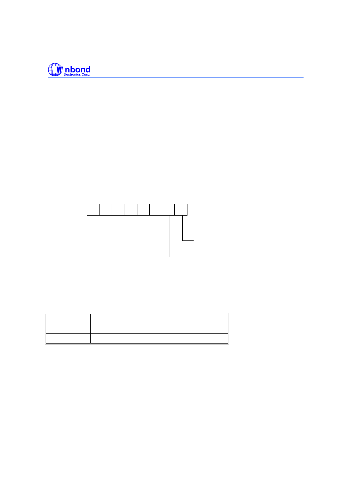
W83697SF
PRELIMINARY
Publication Release Date: April 2001
- 88 - Revision 0.51
9.0 CONFIGURATION REGISTER
9.1 Plug and Play Configuration
The W83697SF uses Compatible PNP pro tocol to access configuration registers for setting up different
types of configurations. In W83697SF, there are eleven Logical Devices (from Logical Device 0 to
Logical Device B with the exception of logical device 4 for backward compatibility) which cor respond to
eleven individual functions: FDC (logical device 0), PRT (logical device 1), UART1 (logical device 2),
UART2 (logical device 3), CIR (Consumer IR, logical device 6), GPIO1 (logical device 7), GPIO5(logical
device 8),GPIO2 ~GPIO4(logical device 9), ACPI ((logical device A), and Hardware monitor (logical
device B). Each Logical Device has its own configuration registers (above CR30). Host can access
those registers by writing an appropriate logical device number into logical device select regist er at CR7.
9.2 Compatible PnP
9.2.1 Extended Function Registers
In Compatible PnP, there are two ways to enter Extended Function and read or write the configuration
registers. HEFRAS (CR26 bit 6) can be used to select one out of these two methods of entering the
Extended Function mode as follows:
HEFRAS address and value
0 write 87h to the location 2Eh twice
1 write 87h to the location 4Eh twice
After Power-on reset, the value on RTSA# (pin 49) is latched by HEFRAS of CR26. In Compatible PnP,
a sp ecific value (87h) must be written twice to the Extended Functions Enable Register (I/O port address
2Eh or 4Eh). Secondly, an index value (02h, 07h- FFh) must be written to the Extended Functions Index
Register (I/O port address 2Eh or 4Eh same as Extended Functions Enable Register) to identify which
configuration register is to be accessed. The designer can then access the desired configuration
register through the Extended Functions Data Register (I/O port address 2Fh or 4Fh).
After programming of the configuration register is finished, an additional value (AAh) should be written to
EFERs to exit the Extended Function mode to prevent unintentional access to those configuration
registers. The designer can also set bit 5 of CR26 (LOCKREG) to high to protect the configuration
registers against accidental accesses.
x x x x x x
DRATE0
DRATE1
01
2
3457
6
Page 94

W83697SF
PRELIMINARY
Publication Release Date: April 2001
- 89 - Revision 0.51
The configuration registers can be reset to their default or hardware settings only by a cold reset (pin MR
= 1). A warm reset will not affect the configuration registers.
9.2.2 Extended Functions Enable Registers (EFERs)
After a power-on reset, the W83697SF enters the default operating mode. Before the W83697SF enters
the extended function mode, a specific value must be programmed into the Extended Function Enable
Register (EFER) so that the extended function register can be accessed. The Extended Function
Enable Registers are write -only registers. On a PC/AT system, their port addresses are 2Eh or 4Eh (as
described in previous section).
9.2.3 Extended Function Index Registers (EFIRs), Extended Function Data Registers(EFDRs)
After the extended function mode is entered, the Extended Function Index Register (EFIR) must be
loaded with an index value (02h, 07h-FEh) to access Configuration Register 0 (CR0), Configuration
Register 7 (CR07) to Con figuration Register FE (CRFE), and so forth through the Extended Function
Data Register (EFDR). The EFIRs are write- only registers with port address 2Eh or 4Eh (as described in
section 12.2.1) on PC/AT systems; the EFDRs are read/write registers with port address 2Fh or 4Fh (as
described in section 9.2.1) on PC/AT systems.
9.3 Configuration Sequence
To program W83697SF configuration registers, the following configuration sequence must be followed:
(1). Enter the extended function mode
(2). Configure the configuration registers
(3). Exit the extended function mode
9.3.1 Enter the extended function mode
To place the chip into the extended function mode, two successive wrtites of 0x87 must be applied to
Extended Function Enable Registers(EFERs, i.e. 2Eh or 4Eh).
9.3.2 Configurate the configuration registers
The chip selects the logical device and activates the desired logical devices through Extended Function
Index Register(EFIR) and Extended Function Data Register(EFDR). EFIR is located at the same address
as EFER, and EFDR is located at address (EFIR+1).
First, write the Logical Device Number (i.e.,0x07) to the EFIR and then write the number of the desired
logical device to the EFDR. If accessing the Chip(Global) Control Registers, this step is not required.
Secondly, write the address of the desired configuration register within the logical device to the EFIR and
then write (or read) the desired configuration register through EFDR.
9.3.3 Exit the extended function mode
To exit the extended function mo de, one write of 0xAA to EFER is required. Once the chip exits the
extended function mode, it is in the normal running mode and is ready to enter the configuration mode.
Page 95

W83697SF
PRELIMINARY
Publication Release Date: April 2001
- 90 - Revision 0.51
9.3.4 Software programming example
The following example is written in Intel 8086 assembly language. It assumes that the EFER is located
at 2Eh, so EFIR is located at 2Eh and EFDR is located at 2Fh. If HEFRAS (CR26 bit 6) is set, 4Eh can
be directly replaced by 4Eh and 2Fh replaced by 4Fh.
;-----------------------------------------------------------------------------------
; Enter the extended function mode ,interruptible double-write |
;-----------------------------------------------------------------------------------
MOV DX,2EH
MOV AL,87H
OUT DX,AL
OUT DX,AL
;----------------------------------------------------------------------------; Configurate logical device 1, configuration register CRF0 |
;----------------------------------------------------------------------------MOV DX,2EH
MOV AL,07H
OUT DX,AL ; point to Logical Device Number Reg.
MOV DX,2FH
MOV AL,01H
OUT DX,AL ; select logical device 1
;
MOV DX,2EH
MOV AL,F0H
OUT DX,AL ; select CRF0
MOV DX,2FH
MOV AL,3CH
OUT DX,AL ; update CRF0 with value 3CH
;-----------------------------------------; Exit extended function mo de |
;-----------------------------------------MOV DX,2EH
MOV AL,AAH
OUT DX,AL
Page 96

W83697SF
PRELIMINARY
Publication Release Date: April 2001
- 91 - Revision 0.51
9.4 Chip (Global) Control Register
CR02 (Default 0x00) (Write only)
Bit [7:1]: Reserved.
Bit 0 = 1 SWRST --> Soft Reset.
CR07
Bit [7:0]: LDNB7 - LDNB0 --> Logical Device Number Bit 7 - 0
CR20 (read only)
Bit [7:0]: DEVIDB7 - DEBIDB0 --> Device ID Bit 7 - Bit 0
= 0x 68 (for W83697SF & W83697SF)
= 0x 60 (for W83697F)
CR21 (read only)
Bit [7:0]: DEVREVB7 - DEBREVB0 --> Device Rev
= 0x1X (for W83697SF)
= 0x0X (for W83697SF)
= 0x1Y (for W83697F)
X : Version change number. (Bit [3:0]) --> begin from 1
Y : Version change number. (Bit [3:0]) --> begin from F
CR22 (Default 0xef)
Bit 7: SCPWD
0 Power down
1 No Power down
Bit 6: URDPWD
0 Power down
1 No Power down
Bit 5: URCPWD
0 Power down
1 No Power down
Page 97

W83697SF
PRELIMINARY
Publication Release Date: April 2001
- 92 - Revision 0.51
Bit 4: Reserved
Bit 3: URBPWD
0 Power down
1 No Power down
Bit 2: URAPWD
0 Power down
1 No Power down
Bit 1: PRTPWD
0 Power down
1 No Power down
Bit 0: FDCPWD
0 Power down
1 No Power down
CR23 (Default 0xfe)
Bit [7:1]: Reserved.
Bit 0: IPD (Immediate Power Down).
When set to 1, it will put the whole chip into power down mode immediately.
CR24 (Default 0s1000ss)
Bit 7: Flash ROM I/F Address Segment (000F0000h ~ 000FFFFFh) enable/disable
0 Enable
1 Disable
Bit 6: CLKSEL(Enable 48Mhz)
0 The clock input on Pin 1 should be 24 MHz.
1 The clock input on Pin 1 should be 48 MHz.
The corresponding power-on setting pin is SOUTB (pin 61).
Bit [5:4]: ROM size select
00 1M
01 2M
10 4M
11 Reserved
Bit 3: MEMW# Select (PIN97)
0 MEMW# Disable
Page 98

W83697SF
PRELIMINARY
Publication Release Date: April 2001
- 93 - Revision 0.51
1 MEMW# Enable
Page 99

W83697SF
PRELIMINARY
Publication Release Date: April 2001
- 94 - Revision 0.51
Bit 2: Flash ROM I/F Address Segment (000E0000h ~ 000EFFFFh) enable/disable
0 Enable
1 Disable
Bit 1 : Enable Flash ROM Interface
0 Flash ROM Interface is enabled after hardware reset
1 Flash ROM Interface is disabled after hardware reset
The corresponding power-on setting pin is PENROM#(pin 52)
Bit 0: PNPCSV
0 The Compatible PnP address select registers have default values.
1 The Compatible PnP address select registers have no default value.
The corresponding power-on setting pin is DTRA# (pin 50).
CR25 (Default 0x00)
Bit 7: SCTRI
Bit 6: URDTRI
Bit 5: URCTRI
Bit 4: Reserved
Bit 3: URBTRI
Bit 2: URATRI
Bit 1: PRTTRI
Bit 0: FDCTRI
CR26 (Default 0x00)
Bit 7: SEL4FDD
0 Select two FDD mode.
1 Select four FDD mode.
Bit 6: HEFRAS
These two bits define how to enable Configuration mode. The corresponding power-on
setting pin is RTSA #(pin 49).
HEFRAS Address and Value
0 Write 87h to the location 2E twice.
1 Write 87h to the location 4E twice.
Page 100

W83697SF
PRELIMINARY
Publication Release Date: April 2001
- 95 - Revision 0.51
Bit 5: LOCKREG
0 Enable R/W Configuration Registers.
1 Disable R/W Configuration Registers.
Bit 4: Reserved
Bit 3: DSFDLGRQ
0 Enable FDC legacy mode on IRQ and DRQ selection, then DO register bit 3 is
effective on selecting IRQ
1 Disable FDC legacy mode on IRQ and DRQ selection, then DO register bit 3 is not
effective on selecting IRQ
Bit 2: DSPRLGRQ
0 Enable PRT legacy mode on IRQ and DRQ selection, then DCR bit 4 is effective on
selecting IRQ
1 Disable PRT legacy mode on IRQ and DRQ selection, then DCR bit 4 is not
effective on selecting IRQ
Bit 1: DSUALGRQ
0 Enable UART A/C legacy mode IRQ selecting, then HCR bit 3 is effective on
selecting IRQ
1 Disable UART A/C legacy mode IRQ selecting, then HCR bit 3 is not effective on
selecting IRQ
Bit 0: DSUBLGRQ
0 Enable UART B/D legacy mode IRQ selecting, then HCR bit 3 is effective on
selecting IRQ
1 Disable UART B/D legacy mode IRQ selecting, then HCR bit 3 is not effective on
selecting IRQ
CR28 (Default 0x00)
Bit [7:4]: Reserved.
Bit [3]: Flash ROM I/F Address Segment (FFE80000h ~ FFEFFFFFh) enable/disable
0 Disable
1 Enable
Bit [2:0]: PRTMODS2 - PRTMODS0
0xx Parallel Port Mode
100 Reserved
101 External FDC Mode
110 Reserved
 Loading...