

Page 1

PCI TO ISA BRIDGE SET
W83628F & W83629D
PRELIMINARY
GENERAL DESCRIPTION
W83628F is a PCI-to-ISA bus conversion IC. W83629D is a condensed centralizer
IC for IRQ and DMA control. W83628F and W83629D together form a complete set
for the PCI-to-ISA bridge.
For the new generation Intel chipset Camino and Whitney, featuring LPC bus, there
is no support for ISA bus and slots. However the demand of ISA devices still exist.
For such case, W83628F plus W83629D are the best companion solution for the
non-ISA chipset. Also the packages of W83628F (128-QFP) and W83629D (48LQFP) had been chosen to be the most economic solution for save the M/B board
layout size and cost.
For the new generation chipset featuring LPC interface and support no ISA bus,
W83627HF/F (Winbond LPC I/O) together with the set of W83628F and W83629D
is the complete solution.
FEATURES
PCI to ISA Bridge
•
Full ISA Bus Support including ISA Masters
•
5V ISA and 3.3V PCI interfaces
•
PC/PCI DMA protocol for Software Transparent
•
IRQ Serializer for ISA Parallel IRQ transfer to Serial IRQ
•
Supports 3 fully ISA Compatible Slots without Buffering
•
PCI Bus at 25MHz, 33MHz and up to 40MHz
•
Supports Programmable ISA Bus Divide the PCI Bus Clock into 3 or 4
•
All ISA Signals can be Isolate
•
Supports Configuration registers for programming performance
PACKAGE
•
128-pin PQFP for W83628F
•
48-pin LQFP for W83629D
Publication Release Date: Dec 1998
- 1 - Revision 0.32
Page 2
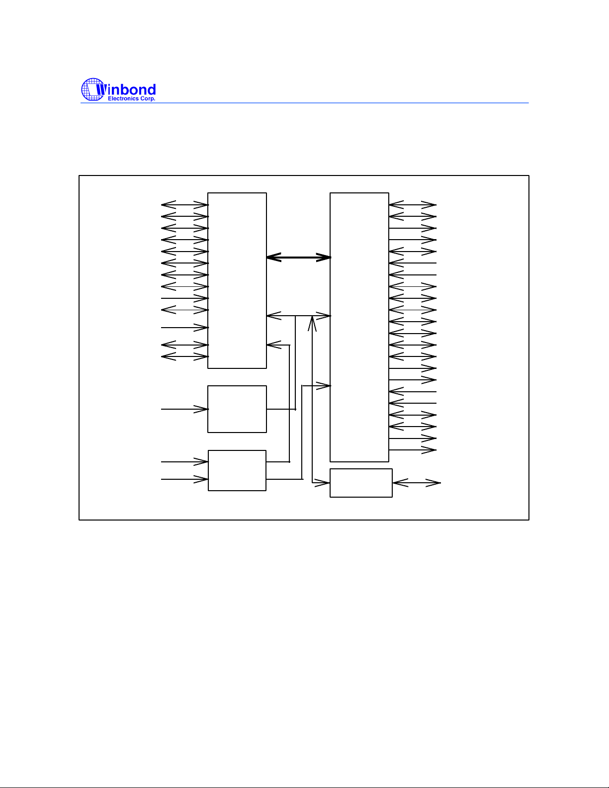
BLOCK DIAGRAM OF W83628F
PCI TO ISA BRIDGE SET
W83628F & W83629D
PRELIMINARY
AD[31:0]
C/BE[3:0]#
PAR
FRAME#
TRDY#
IRDY#
STOP#
DEVSEL#
IDSEL
SERR#
NOGO
PCIRST#
PCICLK
ISOLATE#
3.3V
5V
PCI
Interface
Signal
Isolation
Control
Power
SuppIy
SA[19:0]
SD[15:0]
BALE
AEN
IOCHRDY
IOCS16#
IOCHK#
ISA
Interface
Handshaking HS[2:0]
IOR#
IOW#
LA[23:17]
SBHE#
MEMCS16#
MEMR#
MEMW#
SMEMR#
SMEMW#
ZEROWS#
MASTER#
REFRESH#
ROMCS#
RSTDRV
SYSCLK
Publication Release Date: Jan 1999
- 2 - Revision 0.32
Page 3
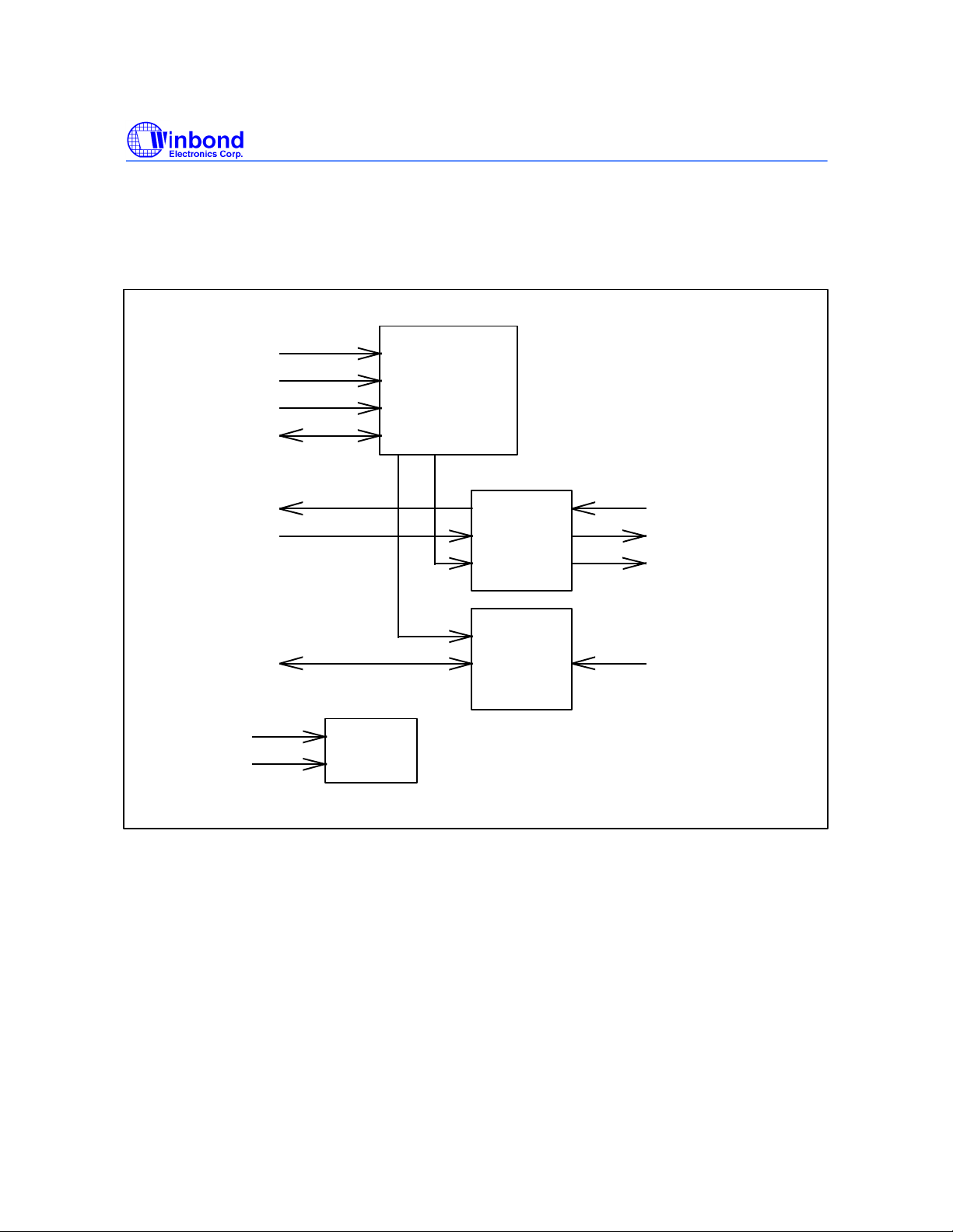
BLOCK DIAGRAM OF W83629D
PCI TO ISA BRIDGE SET
W83628F & W83629D
PRELIMINARY
PCIRST#
PCICLK
NOGO
HS[2:0]
ISAGNT#
3.3V
5V
Power
SuppIy
PCI Host &
Bridge Set
Handshaking
Logic
PCI/PCI
Interface
Serial
to
Parallel
IRQ
DREQ[7:5,3:0]ISAREQ#
DACK[7:5,3:0]#
TC
IRQ[15,14,12:9,7:3]SERIRQ
Publication Release Date: Jan 1999
- 3 - Revision 0.32
Page 4
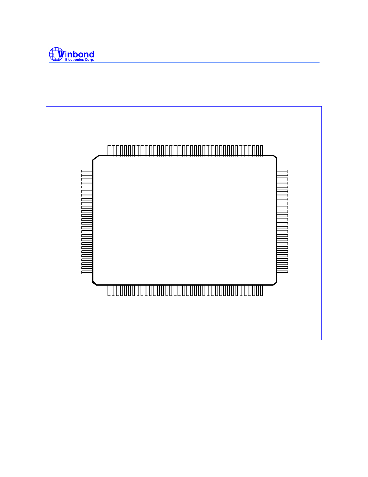
PIN CONFIGURATION FOR 628F
S
Y
S
S
S
S
S
S
S
S
S
C
A
A
V
D
C
6
C
A
D
L
1
1
1
7
K
9
8
7
S
G
A
A
A
A
N
1
1
1
1
D
6
5
4
3
PCI TO ISA BRIDGE SET
W83628F & W83629D
PRELIMINARY
R
I
E
P
S
F
R
C
R
O
R
S
I
O
S
S
S
A
A
A
S
S
S
V
S
S
S
S
S
S
1
1
1
A
A
A
C
A
A
2
1
0
7
9
6
C
5
8
S
A
A
A
A
A
4
3
2
1
0
L
E
N
T
R
A
U
S
O
H
G
#
O
A
D
C
S
T
D
R
S
T
E
0
V
#
#
#
G
A
A
A
A
N
D
D
D
D
D
4
1
2
3
SD5
SD4
IOCHK#
ZEROWS#
SD3
SD2
SD1
SD0
GND
HS2
HS1
HS0
VCC
IOCHRDY
SMEMR#
AEN
SMEMW#
IOR#
IOW#
BALE
MEMCS16#
IOCS16#
LA17
LA18
LA19
GND
103
104
105
106
107
108
109
110
111
112
113
114
115
116
117
118
119
120
121
122
123
124
125
126
127
128
1
1
1
9
0
0
0
9
2
1
0
1 2 345
L
L
L
V
A
A
A
C
2
2
2
C
0
1
2
9
897
L
A
2
3
M
E
M
R
#
L
A
2
2
678 9
969594939
1
0111213
M
S
S
S
E
D
D
D
M
8
9
1
W
0
#
9
1
2
908988878
685
8
8
38281807978
4
W83628F
S
D
1
1
S
S
D
D
1
1
2
3
1
415161718
S
D
1
4
1
222
2
920
324252627
1
M
S
G
A
A
A
A
S
A
B
N
D
S
H
D
1
T
E
5
E
#
R
#
A
D
D
D
D
D
3
3
2
2
2
1
0
9
8
7
7
757
3
V
C
C
282
C
/
B
E
3
#
I
D
S
E
L
7
473
271
9303132
A
A
D
D
2
2
3
2
A
D
2
1
776
A
A
A
D
D
D
2
2
2
6
5
4
7
069
3
3
A
D
2
0
6
6
6
6
867
5
64
3VCC
63
AD5
62
AD6
61
AD7
C/BE0#
60
59
AD8
58
AD9
57
AD10
56
AD11
55
AD12
54
AD13
53
AD14
52
AD15
51
C/BE1#
50
GND
49
PAR
48
PCLK_OUT
47
46
45
44
43
42
41
40
3
3
5
4
A
A
A
D
D
D
1
1
1
9
8
7
39
3
3
3
6
8
7
A
G
D
N
1
D
6
PCICLK
3VCC
SERR#
C/BE2#
DEVSEL#
TRDY#
IRDY#
FRAME#
STOP#
Publication Release Date: Jan 1999
- 4 - Revision 0.32
Page 5
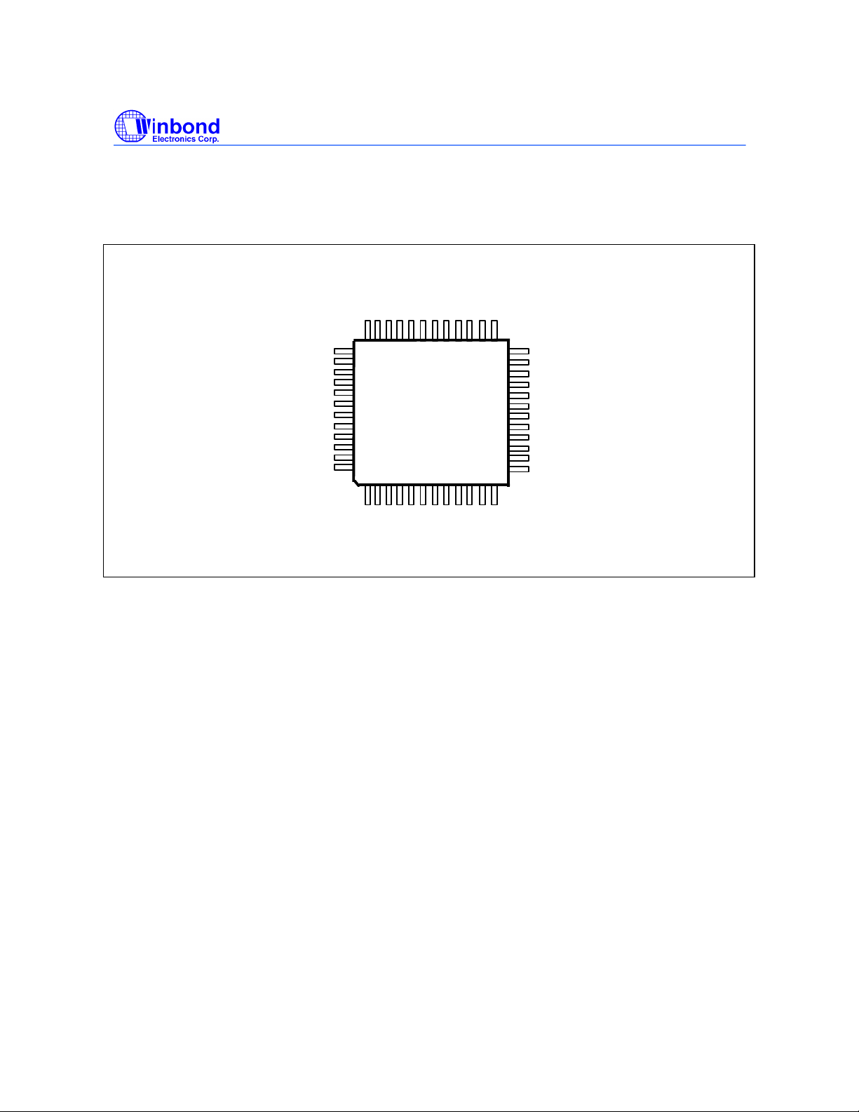
PIN CONFIGURATION FOR 629D
PCI TO ISA BRIDGE SET
W83628F & W83629D
PRELIMINARY
D
D
D
A
D
C
R
K
N
Q
C
7
A
A
D
D
C
R
R
K
Q
Q
6
7
5
#
6
#
D
C
A
D
D
K
G
5
N
#
D
V
C
R
R
C
K
Q
Q
C
3
3
2
NC
NC
NC
NOGO
ISAREQ#
ISAGNT#
GND
PCICLK
NC
SERIRQ
PCIRST#
3VCC
36
37
48
1
I
G
N
R
D
Q
3
W83629D
I
R
Q
4
V
I
I
I
I
C
R
R
R
R
D
Q
Q
Q
Q
C
5
6
7
9
I
I
I
R
R
R
Q
Q
Q
1
1
1
0 124
25
DACK2#
24
DRQ1
DACK1#
DRQ0
DACK0#
TC
GND
HS2
HS1
HS0
VCC
IRQ15
13
12
I
R
Q
1
Publication Release Date: Jan 1999
- 5 - Revision 0.32
Page 6
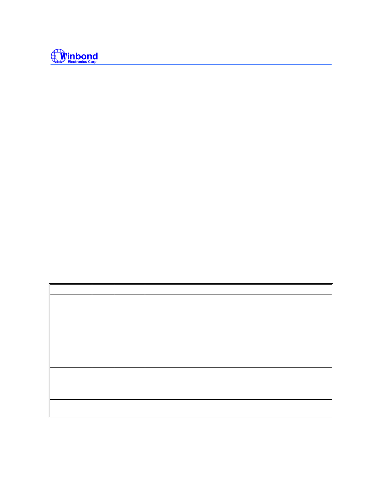
1. PIN DESCRIPTION
Note: Please refer to Section 13.2 DC CHARACTERISTICS for details.
I/O
- TTL level bi-directional pin with 12 mA source-sink capability
12t
I/O
- TTL level bi-directional pin with 24 mA source-sink capability
24t
I/O
- 3.3V TTL level bi-directional pin with 12 mA source-sink capability
12tp3
I/O
- 3.3V TTL level bi-directional pin with 24 mA source-sink capability
24tp3
I/OD
- TTL level bi-directional pin open drain output with 12 mA sink capability
12t
I/O
- TTL level bi-directional pin with 24 mA source-sink capability
24t
OUT
- TTL level output pin with 12 mA source-sink capability
12t
OUT
- TTL level output pin with 24 mA source-sink capability
24t
OUT
OUT
OD12 - Open-drain output pin with 12 mA sink capability
OD24 - Open-drain output pin with 24 mA sink capability
INcs - CMOS level Schmitt-trigger input pin
INt - TTL level input pin
INtd - TTL level input pin with internal pull down resistor
INts - TTL level Schmitt-trigger input pin
IN
- 3.3V TTL level output pin with 12 mA source-sink capability
12tp3
- 3.3V TTL level output pin with 24 mA source-sink capability
24tp3
- 3.3V TTL level Schmitt-trigger input pin
tsp3
PCI TO ISA BRIDGE SET
W83628F & W83629D
PRELIMINARY
1.1 W83628F PIN DESCRIPTION
1.1.1 PCI Interface
SYMBOL PIN I/O FUNCTION
AD[31:0] 19-26
30-37
52-59
61-63
66-70
C/BE[3:0]# 28,45
51,60
PCICLK 47 IN
PCLK_OUT 48
I/O
I/O
OUT
24tp3
24tp3
t
12t
PCI Bus Address and Data Signals. The standard PCI address
and data lines. Address is driven with FRAME# assertion, data is
driven or received in following clocks.
PCI Bus Command and Byte Enables. During the address
phase of a transaction C/BE[3:0]# define the bus command.
During the data phase C/BE[3:0]# are used as Byte Enables.
PCI Bus System Clock. PCICLK provides timing for all
transactions on the PCI bus. All other PCI signals are sampled
on the rising edge of PCICLK, and all timing parameters are
defined with respect to this edge.
PCI Bus System Clock DPLL Output. The PCLK_OUT can
reduce the PCICLK Loading and it produced from internal DPLL.
Publication Release Date: Jan 1999
- 6 - Revision 0.32
Page 7
PCI TO ISA BRIDGE SET
W83628F & W83629D
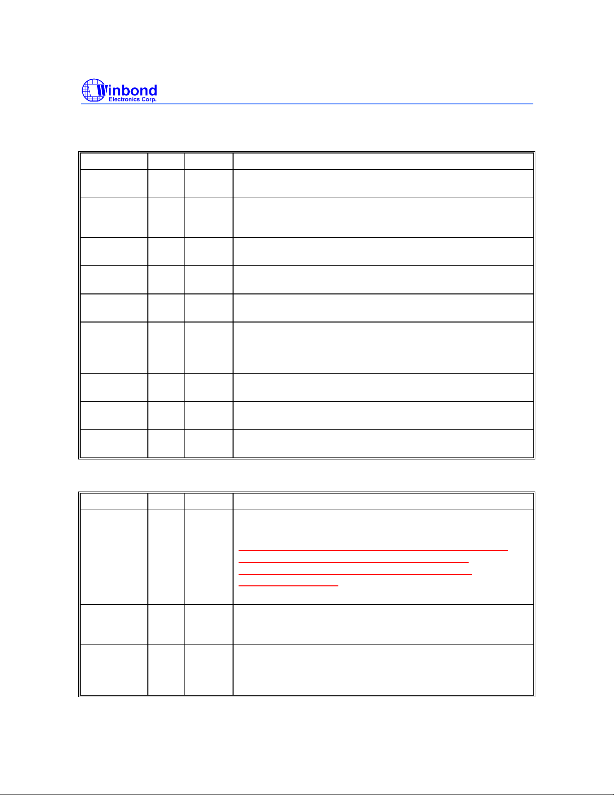
1.1.1 PCI Interface, continued
SYMBOL PIN I/O FUNCTION
FRAME# 40
IDSEL 29 IN
STOP# 39
IRDY# 41
TRDY# 42
DEVSEL# 43
SERR# 45 OD
PAR 49
PCIRST# 71 IN
I/O
I/O
I/O
I/O
I/O
I/O
24tp3
t
12tp3
12tp3
12tp3
12tp3
12
12tp3
t
Frame Signal. FRAME# is driven by the current PCI bus master
to indicate the beginning and duration of an access.
Initialization Device Select. IDSEL is used as a chip select
during configuration read and write transactions. This signal
should be externally tied to one of the upper 21 address signals.
Bus Stop#. STOP# indicates the current target is requesting the
master to stop the current PCI bus transaction.
Initiator Ready. IRDY# indicates the initiating agent ability to
complete the current data phase of the PCI bus transaction.
Target Ready. TRDY# indicates the target agent’s ability to
complete the current data phase of the PCI bus transaction.
Device Select. W83628F drives DEVSEL# to indicate that it is
the target of the current PCI bus transaction. W83628F uses
subtractive decoding and the NOGO protocol to claim PCI
transactions.
System Error. SERR# can be pulsed active by any PCI agent
that detects a system error condition.
Parity Signal. W83628F generates even parity across AD[31:0]
and C/BE[3:0]#.
PCI Reset. W83628F receives PCIRST# as a reset from the PCI
Bus.
PRELIMINARY
1.1.2 Control Logic and Handshaking Signals
SYMBOL PIN I/O FUNCTION
HS[2:0]
112-
114
ISOLATE# 72 IN
NOGO 76 IN
I/O
Handshaking Signals. HS[2:0] connected to W83629D for PCI
12
to ISA SET handshaking signals.
HS1 is handshaking Signal 1, this pin weak pulled-down
during PCIRST# is asserted, and apply a pull-up
resistor(4.7Kohm) to this pin disables ISA bridge
subtraction decoder.
Isolation Control Input. Isolate# is an active low signal by user
t
programming to control the W83628F all output signals to
Isolation and Tri-state.
NOGO, This signal indicates which master initiated the current
t
transaction and also indicates whether or not the current bus
cycle is targeted for the ISA bus. This signal is a point-to-point
connection between PCI HOST Bridge and W83628F.
- 7 - Revision 0.32
Publication Release Date: Jan 1999
Page 8
PCI TO ISA BRIDGE SET
W83628F & W83629D
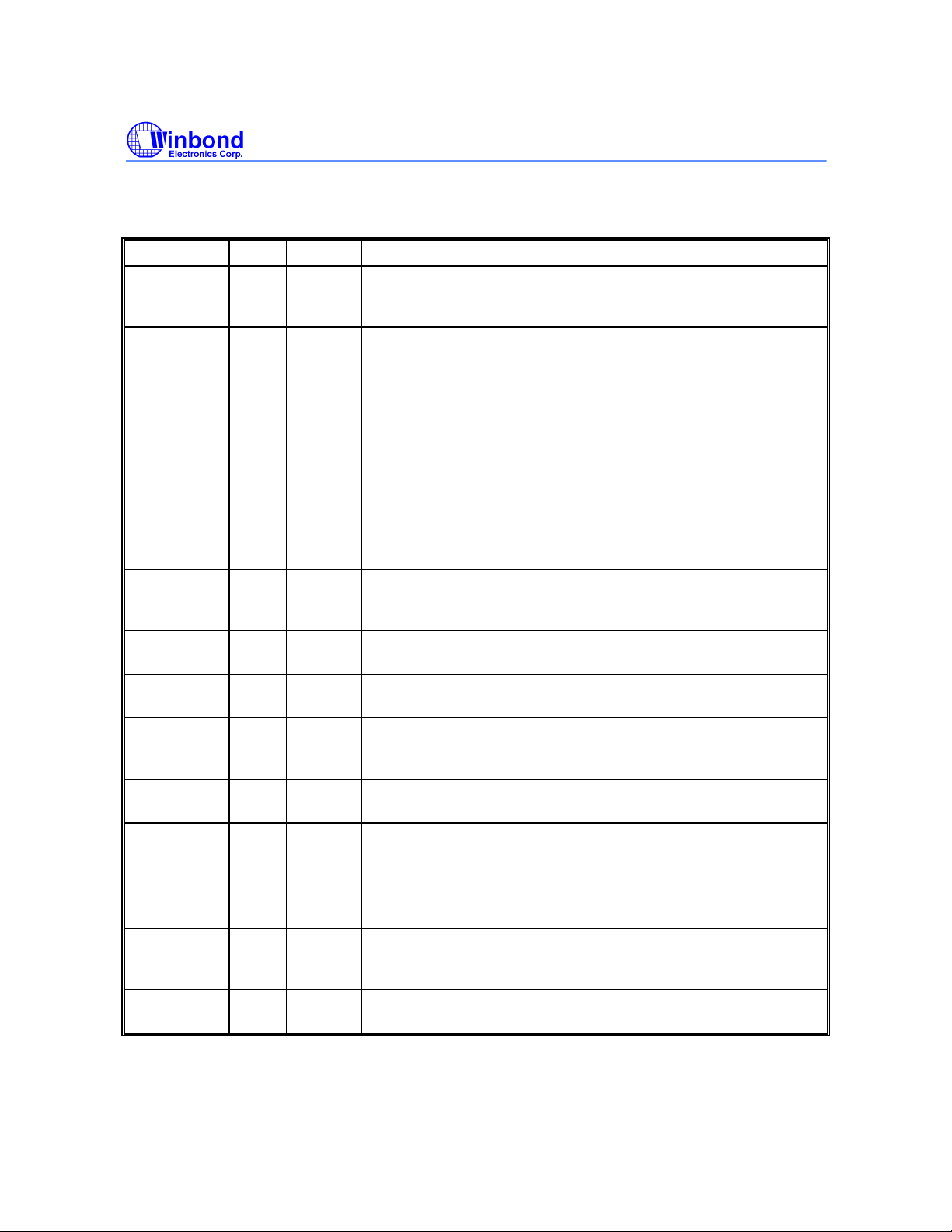
1.1.3 ISA Interface Signals
SYMBOL PIN I/O FUNCTION
SA[19:17] 98-96 OUT
SA[16:0] 94-83
81-77
SD[15:0] 110-
107,
104,
103,
101,
100,
8-15
AEN 118 OUT
IOR# 120 I/O
IOW# 121 I/O
IOCHRDY 116 I/O
SYSCLK 99 OUT
RSTDRV 74 OUT
IOCS16# 124 IN
SBHE# 18 I/O
IOCHK# 105 IN
I/O
I/O
System Address Bus. These are the upper address lines that
24t
define the ISA’s byte granular address space (up to 1 Mbyte).
SA[19:17] are at an unknown state upon PCIRST#.
System Address Bus. These are the bi-directional lower
24t
address lines that define the ISA’s byte granular address space
(up to 1 Mbyte). SA[16:0] are at an unknown state upon
PCIRST#.
System Data. SD[15:0] provide the 16-bit data path for devices
24t
residing on the ISA Bus. The W83628F tri-states SD[15:0] during
PCIRST#.
Address Enable. AEN is asserted during DMA cycles. This
24t
signal is also driven high during W83628F initiated refresh
cycles. AEN is driven low upon PCIRST#.
I/O Read. IOR# is the command to an ISA I/O slave device that
24t
the slave may drive data on to the ISA data bus (SD[15:0]).
I/O Write. IOW# is the command to an ISA I/O slave device that
24t
the slave may latch data from the ISA data bus (SD[15:0]).
I/O Channel Ready. Resources on the ISA Bus negate
24t
IOCHRDY to indicate that additional time (wait states) is required
to complete the cycle.
ISA System Clock. SYSCLK is the reference clock for the ISA
24t
bus. The SYSCLK is generated by dividing PCICLK by 3 or 4.
Reset Drive. W83628F asserts RSTDRV to reset devices that
24t
reside on the ISA Bus. The W83628F asserts this signal while
the PCIRST# is asserted.
16-bit I/O Chip Select. This signal is driven by I/O devices on
t
the ISA Bus to indicate that they support 16-bit I/O bus cycles.
System Byte High Enable. SBHE# asserted indicates that a
24t
byte is being transferred on the upper byte (SD[15:8]) of the data
bus. SBHE# is at an unknown state upon PCIRST#.
I/O Channel Check. IOCHK# can be driven by any resource on
t
the ISA bus during on detection of an error.
PRELIMINARY
Publication Release Date: Jan 1999
- 8 - Revision 0.32
Page 9
PCI TO ISA BRIDGE SET
24t
24t
t
24t
12
24t
t
24t
24t
24t
24
W83628F & W83629D
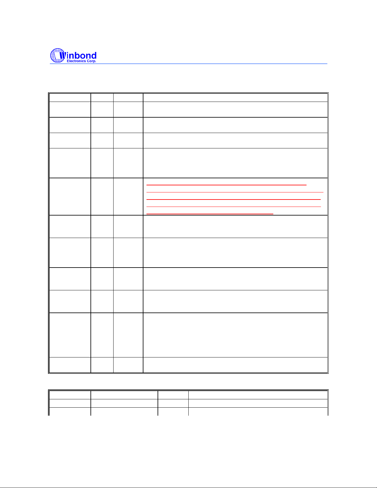
1.1.3 ISA Interface, continued
SYMBOL PIN I/O FUNCTION
MEMR# 6 I/O
MEMW# 7 I/O
MASTER# 17 IN
LA[23:17] 5-2
127-
125
ROMCS# 73 I/O
REFRESH# 75 I/O
ZEROWS# 106 IN
SMEMR# 117 OUT
SMEMW# 119 OUT
BALE 122 OUT
MEMCS16# 123 OD
I/O
Memory Read. MEMR# asserted indicates the current ISA bus
cycle is a memory read.
Memory Write. MEMW# asserted indicates the current ISA bus
cycle is a memory write.
MASTER#. This signal is used with a DREQ line by an ISA
master to gain control of the ISA Bus.
Unlatched Address. The LA[23:17] address lines are bidirectional. These address lines allow accesses to physical
memory on the ISA Bus up to 16 Mbytes. LA[23:17] are outputs
when the W83628F owns the ISA Bus.
ROMCS# ,this pin weak pulled-down during PCIRST is
asserted, and apply a pull-up resistor (4.7 Kohm) to this pin
enable positive decoder of BIOS address range (depend on
Configure register 70 , bit 3,2). When BIOS assress range is
enabled , the PIN is BIOS ROM CS# output.
Refresh. REFRESH# asserted indicates that a refresh cycle is in
progress, or that an ISA master is requesting W83628F to
generate a refresh cycle. Upon PCIRST#, this signal is tri-stated.
Zero Wait States. An ISA slave asserts ZEROWS# after its
address and command signals have been decoded to indicate
that the current cycle can be executed as an ISA zero wait state
cycle. ZEROWS# has no effect during 16-bit I/O cycles.
Standard Memory Read. SMEMR# asserted indicates the
current ISA bus cycle is a memory read cycle to an address
below 1 Mbyte.
Standard Memory Write. SMEMW# asserted indicates the
current ISA bus cycle is a memory write cycle to an address
below 1 Mbyte.
Bus Address Latch Enable. BALE is an active high signal
asserted by the W83628F to indicate that the address (SA[19:0],
LA[23:17]) and SBHE# signal lines are valid.
The LA[23:17] address lines are latched on the trailing edge of
BALE. BALE remains asserted throughout DMA and ISA master
cycles. BALE is driven low upon PCIRST#.
Memory Chip Select 16. MEMCS16# asserted indicates that the
memory slave supports 16-bit accesses.
PRELIMINARY
1.1.4 Power Signals
SYMBOL PIN I/O FUNCTION
VCC 1, 82, 102, 115 PWR
3VCC 27, 46, 64 PWR
5V Supply.
3.3V Supply.
Publication Release Date: Jan 1999
- 9 - Revision 0.32
Page 10

PCI TO ISA BRIDGE SET
W83628F & W83629D
PRELIMINARY
GND 16, 38, 50, 65, 95,
111, 128
PWR
Ground.
Publication Release Date: Jan 1999
- 10 - Revision 0.32
Page 11
PCI TO ISA BRIDGE SET
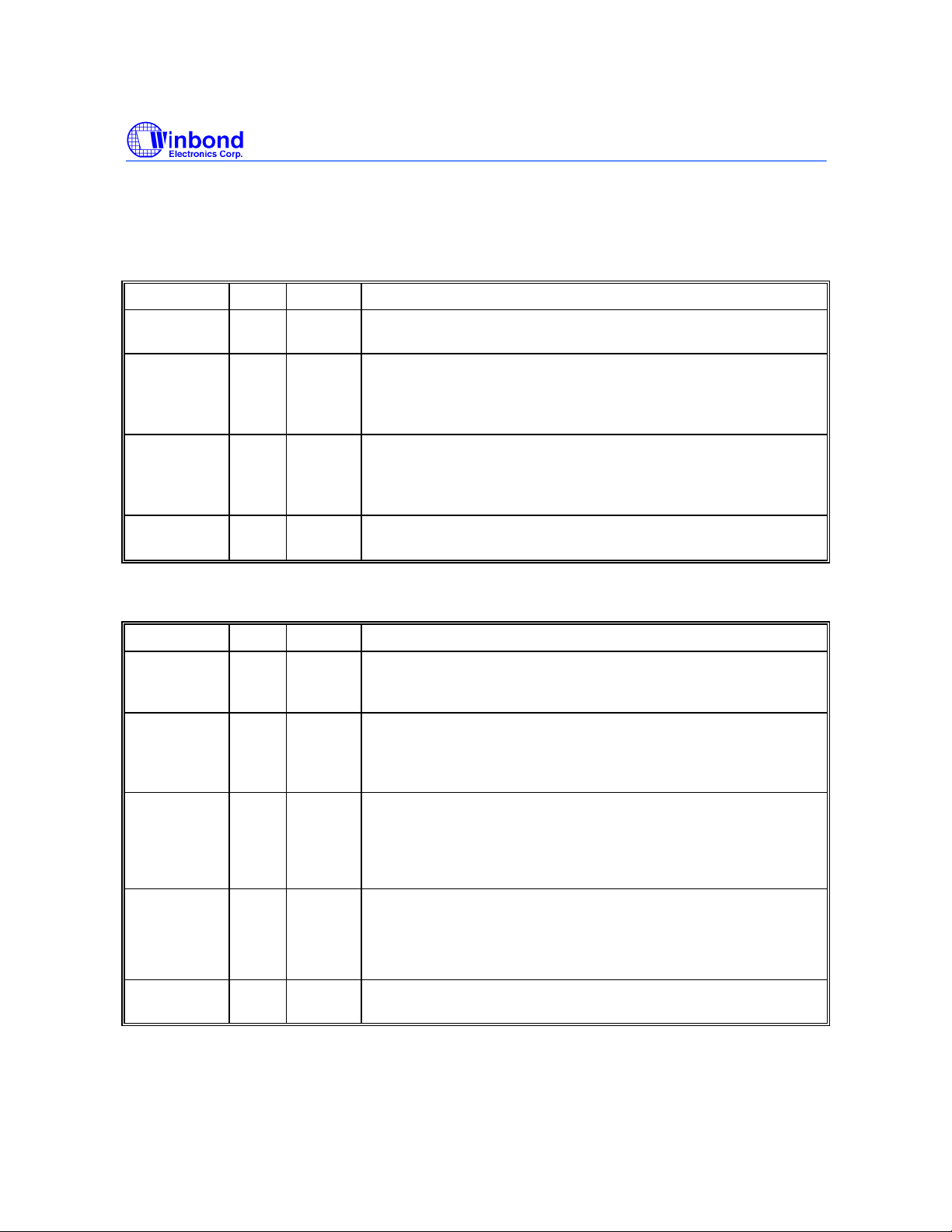
1.2 W83629D PIN DESCRIPTION
1.2.1 Control Logic and Handshaking Signals
SYMBOL PIN I/O FUNCTION
HS[2:0] 17-15
NOGO 40
I/O
IN
Handshaking Signals. HS[2:0] connected to W83628F for PCI
12
to ISA SET handshaking signals.
NO GO. This signal indicates which master initiated the current
t
transaction and also indicates whether or not the current bus
cycle is targeted for the ISA bus. This signal is a point-to-point
connection between PCI HOST Bridge and W83628F.
W83628F & W83629D
PRELIMINARY
PCICLK 44 IN
PCIRST# 47
1.2.2 PC/PCI Interface
SYMBOL PIN I/O FUNCTION
ISAREQ# 41 OUT
ISAGNT# 42
DRQ
[7:5,3:0]
DACK
[7:5,3:0]#
TC 19 OUT
35,33
31,28
26,23
21
34,32
30,27
24,22
20
IN
IN
IN
OUT
PCI Bus System Clock. PCICLK provides timing for all
t
transactions on the PCI bus. All other PCI signals are sampled
on the rising edge of PCICLK, and all timing parameters are
defined with respect to this edge.
PCI Reset. W83628F receives PCIRST# as a reset from the PCI
t
Bus.
ISA Bus Request. This signal is a point-to-point signal between
24t
W83629D and a PCI HOST arbiter . The W83629D asserts this
signal according to the PC/PCI protocol.
ISA Bus Grant. This signal is a point-to-point signal between
t
W83629D and a PCI HOST Bridge’s secondary bus
PCPCIGNT# signal. W83629D asserts this signal according to
the PC/PCI protocol.
DMA Request. The DREQ signal indicates that either a slave
t
DMA device is requesting DMA services, or an ISA bus master is
requesting use of the ISA bus.
DMA Acknowledge. The DACK# signal indicates that either a
24t
DMA channel or an ISA bus master has been granted the ISA
bus.
Terminal Count. The W83628F asserts TC to DMA slaves as a
24t
terminal count indicator.
Publication Release Date: Jan 1999
- 11 - Revision 0.32
Page 12
PCI TO ISA BRIDGE SET
W83628F & W83629D
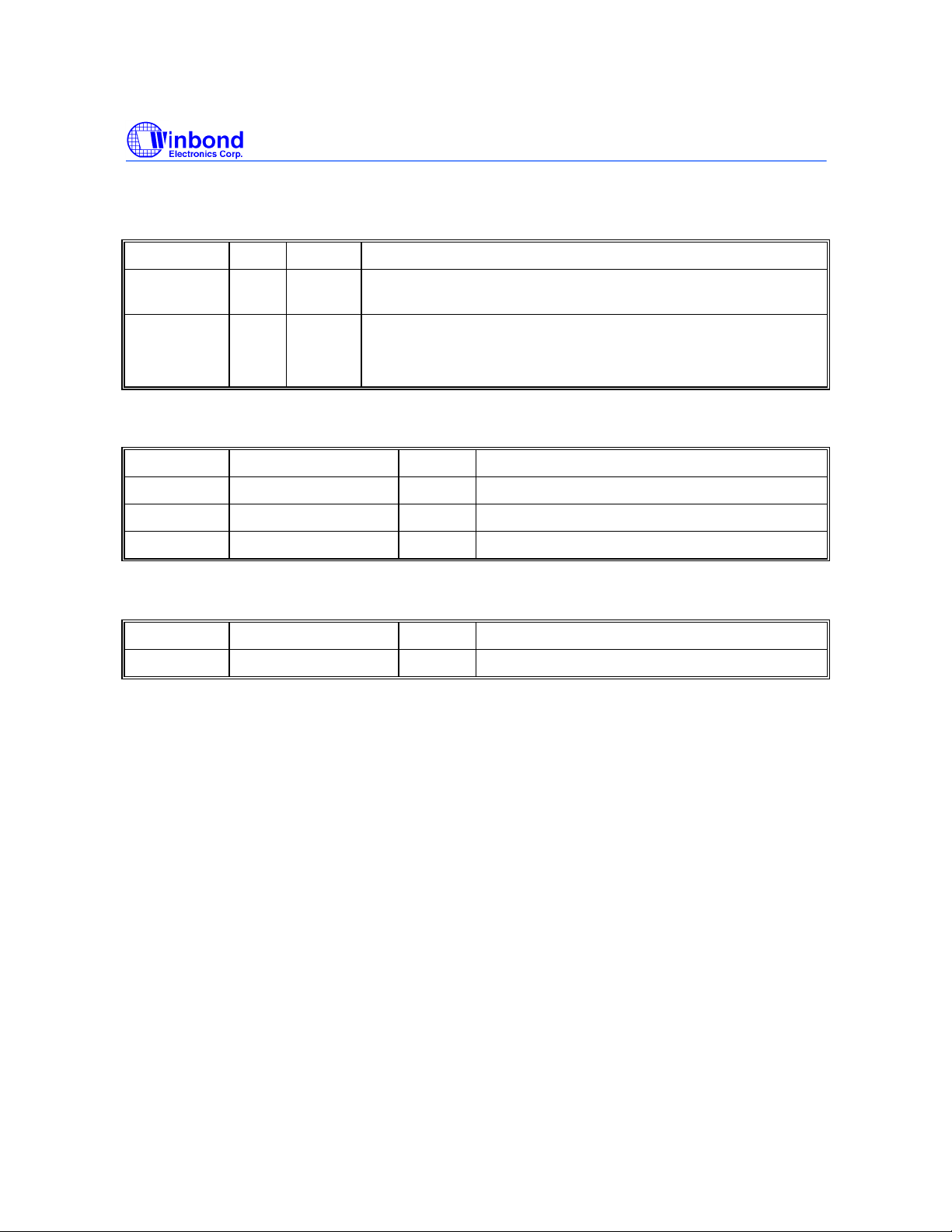
1.2.3 IRQ Serializer Interface
SYMBOL PIN I/O FUNCTION
SERIRQ 46 I/OD
IRQ
[3:7,9:12,14,
15]
1.2.4 Power Signals
SYMBOL PIN I/O FUNCTION
VCC 7, 14, 25 PWR
3VCC 48 PWR
GND 1, 18, 29, 43 PWR
2-6
8-13
IN
Serial Interrupt Requested Signals. This signal is for transfer
12t
IRQ mode between parallel IRQ to serial IRQ.
Parallel Interrupt Requested Input.
t
5V Supply.
3.3V Supply.
Ground.
PRELIMINARY
1.2.5 NC Pins
SYMBOL PIN I/O FUNCTION
NC 36, 37,38, 39, 45
No Connection.
Publication Release Date: Jan 1999
- 12 - Revision 0.32
Page 13

PCI TO ISA BRIDGE SET
W83628F & W83629D
PRELIMINARY
2. PCI CONFIGURATION REGISTERS
2.1 VID-VENDOR IDENTIFICATION REGISTER
Address Offset: 00-01h
Default Value: 1050h
Attribute: Read only
This register is read-only and contains Winbond vendor identification number(1050h).
2.2 DID-DEVICE IDENTIFICATION REGISTER
Address Offset: 02-03h
Default Value: 0628h
Attribute: Read only
This register is read-only and contains the device identification number(0628h).
2.3 PCICMD-PCI COMMAND REGISTER
Address Offset: 04-05h
Default Value: 0007h
Attribute: Read/Write
This register provides control over ISA bridge to generate and response to PCI cycles properly. When
a 0 is written to this register, ISA bridge is to be disconnected from PCI bus for all accesses except
configuration accesses.
Bit 15:10 Reserved.
Bit 9 Fast Back to Back. This bit always returns a zero.
Bit 8 SERR# Enable.
=1 Enable.
=0 Disable.
Bit 7 Wait Cycle Control(Not supported).
Hardwired to zero.
Bit 6 Parity Error Response(Not supported).
Hardwired to zero.
Bit 5 VGA Palette Snoop Enable(Not supported).
Hardwired to zero.
Bit 4 Memory Write and Invalidate Enable(Not supported).
Hardwired to zero.
Publication Release Date: Jan 1999
- 13 - Revision 0.32
Page 14

PCI TO ISA BRIDGE SET
Bit 3 Parity Error Response(Not supported).
Hardwired to zero.
Bit 2 Bus Master Enable.
Hardwired to one. The ISA bridge Bus Masters are always supported to generate a
PCI Bus master cycle.
Bit 1 Memory Space Enable.
Hardwired to one. The ISA bridge Memory space is always enabled.
Bit 0 I/O Space Enable.
Hardwired to one. The ISA bridge I/O space is always enabled.
2.4 PCISTS-PCI STATUS REGISTER
Address Offset: 06-07h
Default Value: 0200h
Attribute: Read/Write
This register shows status information for PCI bus related events.
W83628F & W83629D
PRELIMINARY
Bit 15 Detected Parity Error.
Hardwired to zero. The ISA bridge does not check bus parity.
Bit 14 Signaled System Error.
This bit is set when ISA bridge asserts SERR# on PCI bus.
Bit 13 Received Master Abort Status.
This bit is set when the ISA bridge is target aborted as a master on the PCI bus.
Software sets this bit to 0 by writing a 1 to it.
Bit 12 Received Target Abort Status.
This bit is set when the ISA bridge target aborts a PCI transaction as a target.
Software sets this bit to 0 by writing a 1 to it.
Bit 11 Signaled Target Abort Status.
This bit is set when the ISA bridge signals a target abort for a PCI transaction.
Software sets this bit to 0 by writing a 1 to it.
Bit 10:9 DEVSEL# Timing. This 2 bits always return a 01b(medium decode).
Bit 8 Data Parity Detected(Not supported).
Hardwired to zero.
Bit 7 Fast Back-to-Back(Not supported).
Hardwired to zero.
Publication Release Date: Jan 1999
- 14 - Revision 0.32
Page 15

PCI TO ISA BRIDGE SET
Bit 6 66 MHz/ 33 MHz(Only support 33 MHz).
Hardwired to zero.
Bit 5 User Defineable Features(Not supported).
Hardwired to zero.
Bit 4:0 Reserved.
Reserved and will returns zero when reading this register.
2.5 REVID-REVISION IDENTIFICATION REGISTER
Address Offset: 08h
Default Value: See lastest stepping information
Attribute: Read Only
This register shows status information for PCI bus related events.
Bit 7:0 Revision Identification Number.
W83628F & W83629D
PRELIMINARY
2.6 CCODE-CALSS CODE REGISTER
Address Offset: 09-0Bh
Default Value: 060100h
Attribute: Read Only
The class code register is a read-only register and used to identify the ISA bridge.
Bit 23:16 Base Class Code.
06h = Bus Bridge
Bit 15:8 Sub-Class Code.
01h = PCI to ISA Bridge
Bit 7:0 Programming Interface.
00h
2.7 HEADT-HEAD TYPE REGISTER
Address Offset: 0Eh
Default Value: 00h
Attribute: Read Only
The register is a read-only register and used to indicate that the ISA bridge configuration space
adheres to PCI local bus specification. It also indicates that ISA bridge is not a multifunction device.
Bit 7 Multifunction Indicator.
0 = Not a multifunction device.
Bit 6:0 Layout Code.
00h = PCI layout type.
Publication Release Date: Jan 1999
- 15 - Revision 0.32
Page 16

PCI TO ISA BRIDGE SET
W83628F & W83629D
PRELIMINARY
2.8 IO_RCVR-IO RECOVERY REGISTER
Address Offset: 40h
Default Value: 4Dh
Attribute: Read/Write
Bit 7 SYSCLK Divider.
0 = SYSCLK is equal to PCICLK divided by 4.
1 = SYSCLK is equal to PCICLK divided by 3.
Bit 6 8-bit I/O Recovery Enable
0 = Disable bits 5:3 setting and uses 3.5 SYSCLKs for 8 bit I/O recovery time.
1 = Enable bits 5:3 setting.
Bit 5:3 8-bit I/O RecoveryTimes.
When bit 6=1 ,this 3-bit field defines the additional number of SYSCLKs added
to standard 3.5 SYSCLK recovery time for 8 bit I/O
000 =0 SYSCLK
001 =1 SYSCLK
010 =2 SYSCLKs
011 =3 SYSCLKs
100 =4 SYSCLKs
101 =5 SYSCLKs
110 =6 SYSCLKs
111 = 7 SYSCLKs
Bit 2 16-bit I/O Recovery Enable.
= 0 Ignore bits 1:0 setting and uses 3.5 SYSCLKs for 16-bit I/O recovery time.
= 1 The 16-bit I/O recovery time is decided by bits 1:0.
Bit 1:0 16-bit I/O Recovery Times.
When bit 2=1 ,this 2-bit field defines the additional number of SYSCLKs added
to standard 3.5 SYSCLK recovery time for 16 bit I/O
= 01 1 SYSCLK
= 10 2 SYSCLKs
= 11 3 SYSCLKs
= 00 4 SYSCLKs
2.9 WISA_STS-ISA BRIDGE ERROR STATUS REGISTER
Address Offset: 42h
Default Value: 00h
Publication Release Date: Jan 1999
- 16 - Revision 0.32
Page 17

PCI TO ISA BRIDGE SET
W83628F & W83629D
PRELIMINARY
Attribute: Read/Write
Bit 7:3 Reserved.
Bit 2 IOCHK# Pin State.
This bit reflects the inverse state of IOCHK# pin on the ISA bus.
Bit 1 Reserved.
Bit 0 Byte Lane Error.
This bit is set if the ISA bridge detects an illegal byte lane combination for a
PCI I/O cycles.
2.10 WISA_FADC-ISA BRIDGE FAST DECODERS CONTROL REGISTER
Address Offset: 50h
Default Value: 00h
Attribute: Read/Write
Bit 7 Enable/Disable Fast I/O Address Decoder # 7.
Bit 6 Enable/Disable Fast I/O Address Decoder # 6.
Bit 5 Enable/Disable Fast I/O Address Decoder # 5.
Bit 4 Enable/Disable Fast I/O Address Decoder # 4.
Bit 3 Enable/Disable Fast I/O Address Decoder # 3.
Bit 2 Enable/Disable Fast I/O Address Decoder # 2.
Bit 1 Enable/Disable Fast I/O Address Decoder # 1.
Bit 0 Enable/Disable Fast I/O Address Decoder # 0.
2.11 WISA_FAD0MC-ISA BRIDGE FAST DECODERS # 0 MASK CONTROL
REGISTER
Address Offset: 58h
Default Value: 00h
Attribute: Read/Write
This register is used to mask address bits(A7~A0) for fast address decoder # 0, if the corresponding
bit of this register is set to a 1, the corresponding address bit(A7~A0) is ignore by the faster address
decoder # 0.
Publication Release Date: Jan 1999
- 17 - Revision 0.32
Page 18

PCI TO ISA BRIDGE SET
W83628F & W83629D
PRELIMINARY
2.12 WISA_FAD0MC-ISA BRIDGE FAST DECODERS # 1 MASK CONTROL
REGISTER
Address Offset: 59h
Default Value: 00h
Attribute: Read/Write
This register is used to mask address bits(A7~A0) for fast address decoder # 1, if the corresponding
bit of this register is set to a 1, the corresponding address bit(A7~A0) is ignore by the faster address
decoder # 1.
2.13 WISA_FAD0MC-ISA BRIDGE FAST DECODERS # 2 MASK CONTROL
REGISTER
Address Offset: 5Ah
Default Value: 00h
Attribute: Read/Write
This register is used to mask address bits(A7~A0) for fast address decoder # 2, if the corresponding
bit of this register is set to a 1, the corresponding address bit(A7~A0) is ignore by the faster address
decoder # 2.
2.14 WISA_FAD0MC-ISA BRIDGE FAST DECODERS # 3 MASK CONTROL
REGISTER
Address Offset: 5Bh
Default Value: 00h
Attribute: Read/Write
This register is used to mask address bits(A7~A0) for fast address decoder # 3, if the corresponding
bit of this register is set to a 1, the corresponding address bit(A7~A0) is ignore by the faster address
decoder # 3.
2.15 WISA_FAD0MC-ISA BRIDGE FAST DECODERS # 4 MASK CONTROL
REGISTER
Address Offset: 5Ch
Default Value: 00h
Attribute: Read/Write
This register is used to mask address bits(A7~A0) for fast address decoder # 4, if the corresponding
bit of this register is set to a 1, the corresponding address bit(A7~A0) is ignore by the faster address
decoder # 4.
Publication Release Date: Jan 1999
- 18 - Revision 0.32
Page 19

PCI TO ISA BRIDGE SET
W83628F & W83629D
PRELIMINARY
2.16 WISA_FAD0MC-ISA BRIDGE FAST DECODERS # 5 MASK CONTROL
REGISTER
Address Offset: 5Dh
Default Value: 00h
Attribute: Read/Write
This register is used to mask address bits(A7~A0) for fast address decoder # 5, if the corresponding
bit of this register is set to a 1, the corresponding address bit(A7~A0) is ignore by the faster address
decoder # 5.
2.17 WISA_FAD0MC-ISA BRIDGE FAST DECODERS # 6 MASK CONTROL
REGISTER
Address Offset: 5Eh
Default Value: 00h
Attribute: Read/Write
This register is used to mask address bits(A7~A0) for fast address decoder # 6, if the corresponding
bit of this register is set to a 1, the corresponding address bit(A7~A0) is ignore by the faster address
decoder # 6.
2.18 WISA_FAD0MC-ISA BRIDGE FAST DECODERS # 7 MASK CONTROL
REGISTER
Address Offset: 5Fh
Default Value: 00h
Attribute: Read/Write
This register is used to mask address bits(A7~A0) for fast address decoder # 7, if the corresponding
bit of this register is set to a 1, the corresponding address bit(A7~A0) is ignore by the faster address
decoder # 7.
2.19 WISA_FADCB0-ISA BRIDGE FAST DECODERS # 0 BASE ADDRESS
REGISTER
Address Offset: 60-61h**
Default Value: 0000h
Attribute: Read/Write
This register contains the base address for fast address decoder # 0.A
**Note: 60h is lower byte and 61h is upper byte.
Publication Release Date: Jan 1999
- 19 - Revision 0.32
Page 20

PCI TO ISA BRIDGE SET
W83628F & W83629D
PRELIMINARY
2.20 WISA_FADCB1-ISA BRIDGE FAST DECODERS # 1 BASE ADDRESS
REGISTER
Address Offset: 62-63h
Default Value: 0000h
Attribute: Read/Write
This register contains the base address for fast address decoder # 1.
2.21 WISA_FADCB2-ISA BRIDGE FAST DECODERS # 2 BASE ADDRESS
REGISTER
Address Offset: 64-65h
Default Value: 0000h
Attribute: Read/Write
This register contains the base address for fast address decoder # 2.
2.22 WISA_FADCB3-ISA BRIDGE FAST DECODERS # 3 BASE ADDRESS
REGISTER
Address Offset: 66-67h
Default Value: 0000h
Attribute: Read/Write
This register contains the base address for fast address decoder # 3.
2.23 WISA_FADCB4-ISA BRIDGE FAST DECODERS # 4 BASE ADDRESS
REGISTER
Address Offset: 68-69h
Default Value: 0000h
Attribute: Read/Write
This register contains the base address for fast address decoder # 4.
2.24 WISA_FADCB5-ISA BRIDGE FAST DECODERS # 5 BASE ADDRESS
REGISTER
Address Offset: 6A-6Bh
Default Value: 0000h
Attribute: Read/Write
This register contains the base address for fast address decoder # 5.
Publication Release Date: Jan 1999
- 20 - Revision 0.32
Page 21

PCI TO ISA BRIDGE SET
W83628F & W83629D
PRELIMINARY
2.25 WISA_FADCB6-ISA BRIDGE FAST DECODERS # 6 BASE ADDRESS
REGISTER
Address Offset: 6C-6Dh
Default Value: 0000h
Attribute: Read/Write
This register contains the base address for fast address decoder # 6.
2.26 WISA_FADCB7-ISA BRIDGE FAST DECODERS # 6 BASE ADDRESS
REGISTER
Address Offset: 6E-6Fh
Default Value: 0000h
Attribute: Read/Write
This register contains the base address for fast address decoder # 0.
2.27 WISA_CTRLREG1-ISA BRIDGE CONTROL REGISTER 1
Address Offset: 70h
Default Value: 000001ssb
Attribute: Read/Write
Power-on setting bits bit 1:0 are power-on set by ROMCS# and HS1.
Bit 7-6 Reserved.
Bit 5-4 = 00 Send AD Bus with no STEP
= 01 Send AD Bus with 2 STEP
= 10 Send AD Bus with 4 STEP
= 11 Reverse
Bit 3-2 = 00 1MB BIOS ROM positive decode.
= 01 2MB BIOS ROM positive decode.
= 10 4MB BIOS ROM positive decode.
= 11 8MB BIOS ROM positive decode.
Bit 1 =0 Disable High-Address BIOS ROM decoder.
=1 Enable High-Address BIOS ROM decoder.
This bit can be set/reset by ROMCS# power-on setting during PCIRST# assert.
Bit 0 =0 Normal mode.
=1 Disable ISA Bridge subtraction decoder.
This bit can be set/reset by HS1 power-on setting during PCIRST# assert.
Publication Release Date: Jan 1999
- 21 - Revision 0.32
Page 22

PCI TO ISA BRIDGE SET
W83628F & W83629D
2.28 WISA_CTRLREG2-ISA BRIDGE CONTROL REGISTER 2
Address Offset: 71h
Default Value: 00h
Attribute: Read/Write
Bit7 =0 Enable IRQ11.
=1 Disable IRQ11.
Bit 6 =0 Enable IRQ10.
=1 Disable IRQ10.
Bit 5 =0 Enable IRQ9.
=1 Disable IRQ9.
Bit 4 =0 Enable IRQ7.
=1 Disable IRQ7.
Bit 3 =0 Enable IRQ6.
=1 Disable IRQ6.
Bit 2 =0 Enable IRQ5.
=1 Disable IRQ5.
Bit 1 =0 Enable IRQ4.
=1 Disable IRQ4.
Bit 0 =0 Enable IRQ3.
=1 Disable IRQ3.
PRELIMINARY
2.29 WISA_CTRLREG3-ISA BRIDGE CONTROL REGISTER 3
Address Offset: 72h
Default Value: 00h
Attribute: Read/Write
Bit 7-3 Reserved.
Bit 2 =0 Enable IRQ15.
=1 Disable IRQ15.
Bit 1 =0 Enable IRQ14.
=1 Disable IRQ14.
Bit 0 =0 Enable IRQ12.
=1 Disable IRQ12.
Publication Release Date: Jan 1999
- 22 - Revision 0.32
Page 23

PCI TO ISA BRIDGE SET
W83628F & W83629D
2.30 WISA_CTRLREG4-ISA BRIDGE CONTROL REGISTER 4
Address Offset: 73h
Default Value: 00h
Attribute: Read/Write
Bit7 =0 Enable DRQ 7.
=1 Disable DRQ 7.
Bit 6 =0 Enable DRQ6.
=1 Disable DRQ6.
Bit 5 =0 Enable DRQ5.
=1 Disable DRQ5.
Bit 4 Reserved.
Bit 3 =0 Enable DRQ 3.
=1 Disable DRQ 3.
Bit 2 =0 Enable DRQ 2.
=1 Disable DRQ 2.
Bit 1 =0 Enable DRQ 1.
=1 Disable DRQ 1.
Bit 0 =0 Enable DRQ 0.
=1 Disable DRQ 0.
PRELIMINARY
2.31 WISA_TSTREG-ISA BRIDGE TEST REGISTER
Address Offset: 80h
Default Value: 04h
Attribute: Read/Write
Bit 7-5 Reserved and should not write data to this register.
Bit 4 =0 80h port decoding on subtrastive cycles of LPC I/F.
=1 80h port decoding on positive cycles of LPC I/F.
This Bit must be set 1when LPC I/F is only decoding on positive cycles,but
when the bridge is used in PIIX4 for test set the bit to 0 .
Bit 3 Reserved and should not write data to this register.
Bit 2-0 000 - 0.8 nS. For Winbond Internal Reference only.
001 - 0.6 nS.
Publication Release Date: Jan 1999
- 23 - Revision 0.32
Page 24

010 - 0.4 nS.
011 - 0.2 nS.
100 0 nS.
101 +0.2 nS.
110 +0.4 nS.
111 +0.6 nS.
PCI TO ISA BRIDGE SET
W83628F & W83629D
PRELIMINARY
Publication Release Date: Jan 1999
- 24 - Revision 0.32
Page 25
PCI TO ISA BRIDGE SET
W83628F & W83629D
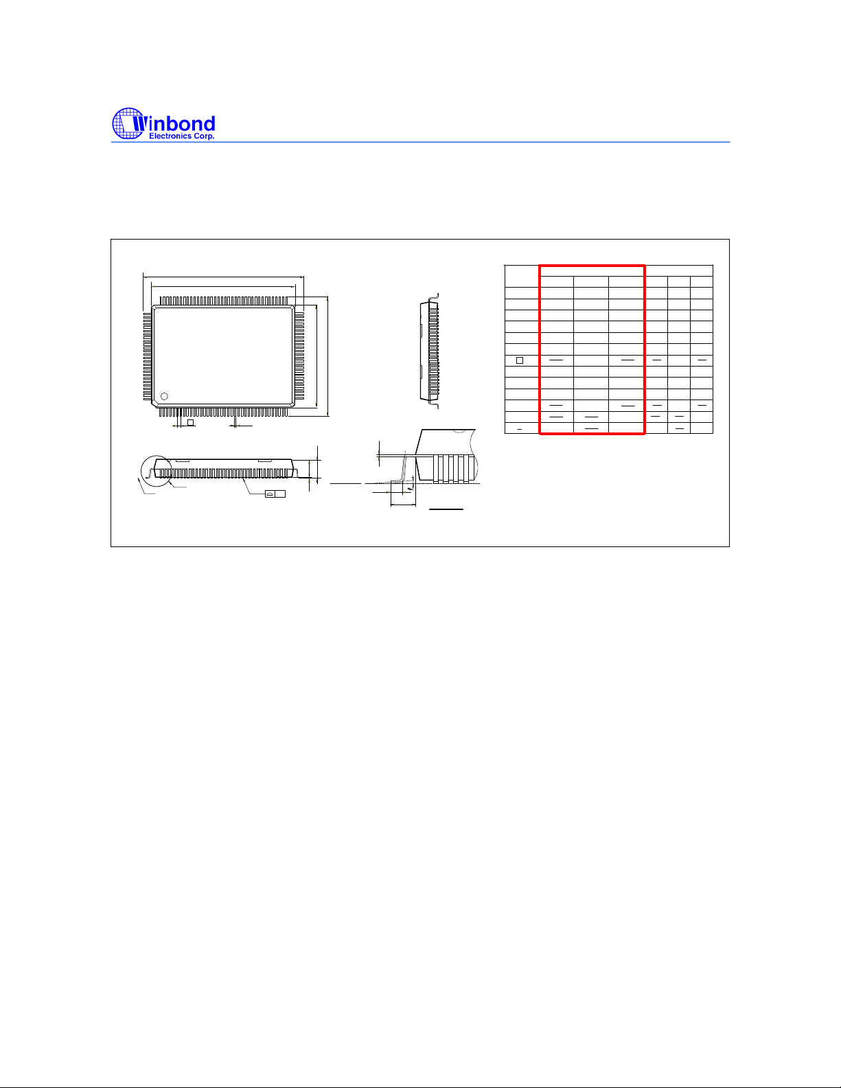
3. PACKAGE DIMENSIONS 1 FOR W83628F (128-PIN PQFP)
PRELIMINARY
103
128
102
1
Seating Plane
e
See Detail F
H
E
E
65
64
Symbol
1
A
A
2
b
c
D
H
DD
E
e
HD
H
E
39
38
b
A
2
A
1
A
y
c
L
L
1
Detail F
L
1
L
y
0
Note:
1.Dimension D & E do not include interlead
2.Dimension b does not include dambar
3.Controlling dimension : Millimeter
4.General appearance spec. should be based
5. PCB layout please use the "mm".
Dimension in mm
Min Nom Max
0.25
0.35 0.45
2.72
2.57
0.10
0.20
0.10
0.15
14.00
13.90
19.90 20.00 20.10
0.50
17.20
17.00
23.00 23.20
0.80
0.65
1.60
0
flash.
protrusion/intrusion
on final visual inspection spec.
.
2.87
0.30
0.20
14.10
17.40
23.40
0.95
0.08
7
Dimension in inch
MaxNomMin
0.010
0.014 0.018
0.113
0.107
0.101
0.004
0.004
0.547
0.783 0.787 0.791
0.669
0.905 0.913 0.921
0.025
0.012
0.008
0.008
0.006
0.555
0.551
0.020
0.685
0.677
0.037
0.031
0.063
0.003
0
7
Publication Release Date: Jan 1999
- 25 - Revision 0.32
Page 26
PCI TO ISA BRIDGE SET
W83628F & W83629D
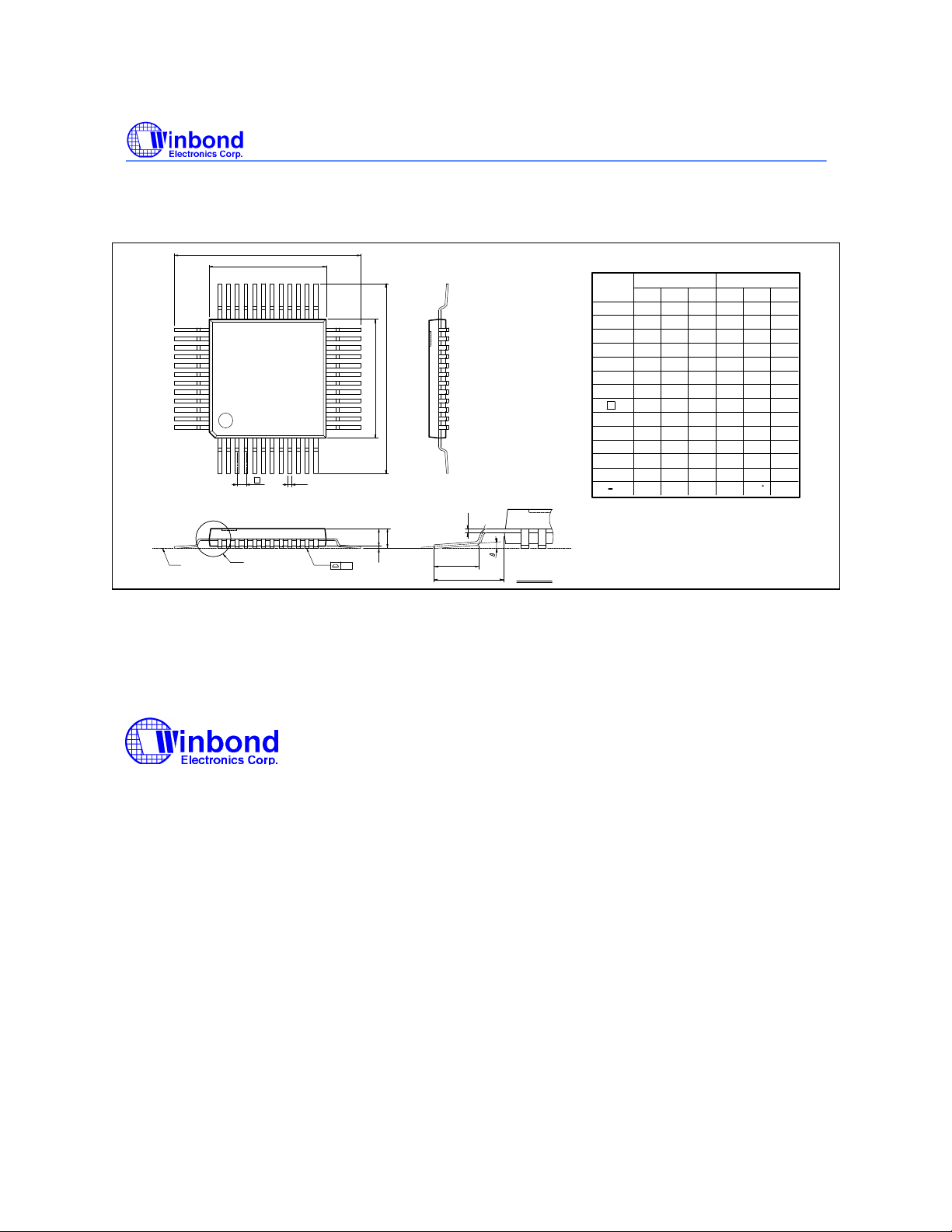
4. PACKAGE DIMENSIONS 2 FOR W83629D (48-PIN LQFP)
H
D
D
25
Symbol
A
1
24
A
2
A
b
E
E
H
13
c
D
E
e
D
H
H
E
L
1
L
12
b
c
A
2
A
1
A
y
L
L
1
Detail F
y
0
Notes:
1. Dimensions D & E do not include interlead
flash.
2. Dimension b does not include dambar
protrusion/intrusion.
3. Controlling dimension: Millimeters
4. General appearance spec. should be based
on final visual inspection spec.
37
48
Seating Plane
36
1
e
See Detail F
PRELIMINARY
Dimension in inch Dimension in mm
Min. Nom. Max. Max.Nom.Min.
---
---
0.05
---
1.35
1.40
0.20
0.17 0.27
---
0.09
7.00
7.00
0.50
9.00
9.00
0.45
0.60
1.00
--- ---
0.08
3.5 7
0
1.60
0.15
1.45
0.20
0.75
Headquarters
No. 4, Creation Rd. III
Science-Based Industrial Park
Hsinchu, Taiwan
TEL: 886-35-770066
FAX: 886-35-789467
www: http://www.winbond.com.tw/
Winbond Electronics (H.K.) Ltd.
Rm. 803, World Trade Square, Tower II
123 Hoi Bun Rd., Kwun Tong
Kowloon, Hong Kong
TEL: 852-27516023-7
FAX: 852-27552064
Winbond Electronics
(North America) Corp.
2730 Orchard Parkway
San Jose, CA 95134 U.S.A.
TEL: 1-408-9436666
FAX: 1-408-9436668
Taipei Office
11F, No. 115, Sec. 3, Min-Sheng East Rd.
Taipei, Taiwan
TEL: 886-2-7190505
FAX: 886-2-7197502
TLX: 16485 WINTPE
Please note that all data and specifications are subject to change without notice. All the trade marks
of products and companies mentioned in this data sheet belong to their original owners
Publication Release Date: Jan 1999
- 26 - Revision 0.32
Page 27

PCI TO ISA BRIDGE SET
W83628F & W83629D
PRELIMINARY
5. REVISION NOTICES.
1998.11.16 Add High-Address BIOS ROM decoder function(CS#/HS3). (Page 7 & Page 20)
1998.11.19 Change decode range to #FFF00000~#FFFFFFFF & #000E0000~#000FFFFF.
1999.01.17 Supports 3 fully ISA Compatible Slots without Buffering
Rename HS3. it is renamed to ROMCS# in W83628F,and NC in W83629D.
1999.04.21 Indicate the Bit 4 of offset address 80h is used to enable 80h port decoding
when
only positive decoding switched of LPC I/F.
Publication Release Date: Jan 1999
- 27 - Revision 0.32
 Loading...