

Page 1

Winbond W83626F
LPC-to-ISA Bridge
Page 2
W83626F/W83626D
W83626F/W83626D Data Sheet Revision History
Pages Dates Version
1 n.a. 02/25/00 0.50 0.50 First published.
2
3
4
5
6
7
8
9
Version
on Web
Main Contents
10
Please note that all data and specifications are subject to change without notice. All
the trade marks of products and companies mentioned in this data sheet belong to
their respective owners.
LIFE SUPPORT APPLICATIONS
These products are not designed for use in life support appliances, devices, or
systems where malfunction of these products can reasonably be expected to result
in personal injury. Winbond customers using or selling these products for use in
such applications do so at their own risk and agree to fully indemnify Winbond for
any damages resulting from such improper use or sales.
Publication Release Date:Feb. 2000
-I - Preliminary Revision 0.50
Page 3

LPC TO ISA BRIDGE SET
W83626F/W83626D
PRELIMINARY
GENERAL DESCRIPTION
W83626F/W83626D is a transparent LPC-to-ISA bus conversion IC.
For the new generation Intel chipset Camino and Whitney, SiS Super South 960,
featuring LPC bus, there is no support for ISA bus and slots. However the demand of
ISA devices still exist. For such case, W83626F is the best companion solution for the
non-ISA chipset. Also the packages of W83626F had been chosen to be the most
economic solution for save the M/B board layout size and cost.
For the new generation chipset featuring LPC interface and support no ISA bus,
W83627HF (Winbond LPC I/O) together with the set of W83626F is the complete
solution.
FEATURES
LPC to ISA Bridge
•
Meet LPC Spec. 1.1
•
Support LDRQ# (LPC DMA), SERIRQ (serial IRQ)
•
Full ISA Bus Support except ISA Bus Masters
•
5V ISA and 3.3V LPC interfaces
•
All Software Transparent
•
IRQ Serializer for ISA Parallel IRQ transfer to Serial IRQ
Supports 3 fully ISA Compatible Slots without Buffering
•
•
LPC Bus at 33MHz
•
Supports Programmable ISA Bus Divide the PCI Clock into 3 or 4
•
All ISA Signals can be Isolate
•
14.318MHz in to generate two 14.318MHz buffer out and one 24.576MHz
•
Specific Keyboard Functions supported
Support 8 programmable general purpose I/O pins
•
Supports Configuration registers for programming performance
•
PACKAGE
• 128-pin PQFP for W83626F
Publication Release Date: Feb 2000
- 1 - Revision 0.50
Page 4
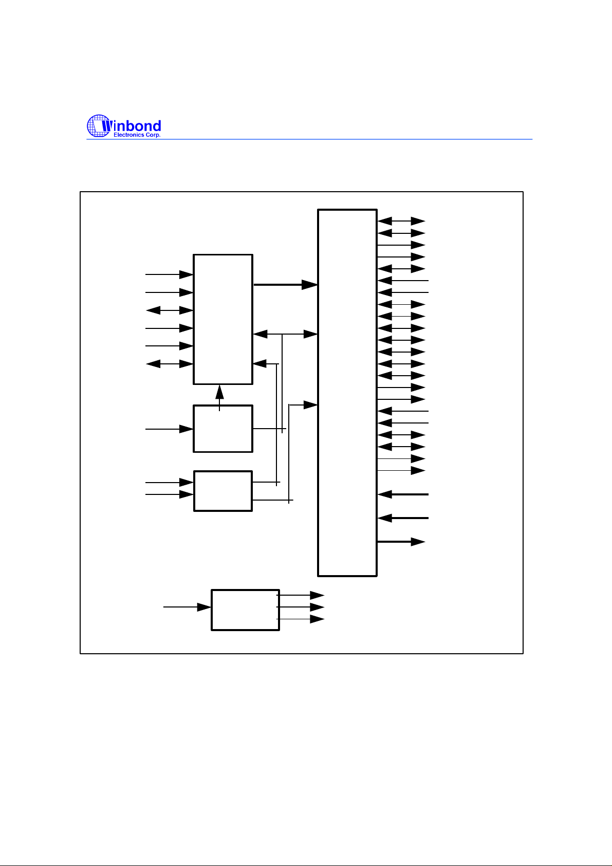
Block diagram OF W83626F
LFRAM#
PCIRST#
LAD[3:0]
PCICLK
LDRQ#
SERIRQ
ISOLATE#
3.3V
5V
Interface
Signal
Isolation
Control
Power
SuppIy
LPC
LPC TO ISA BRIDGE SET
W83626F/W83626D
PRELIMINARY
SA[19:0]
SD[15:0]
BALE
AEN
IOCHRDY
IOCS16#
IOCHK#
ISA
Interface
IOR#
IOW#
LA[23:17]
SBHE#
MEMCS16#
MEMR#
MEMW#
SMEMR#
SMEMW#
ZEROWS#
MASTER#
REFRESH#
ROMCS#
RSTDRV
SYSCLK
IRQ[3:7,9:12,14,15]
DRQ[0:3,5:7]
DACK[0:3,5:7]
14.318M
CLOCK
GEN. / BUF.
- 2 - Revision 0.50
14MOUT1
14MOUT2
24.576M
Publication Release Date: Feb 2000
Page 5
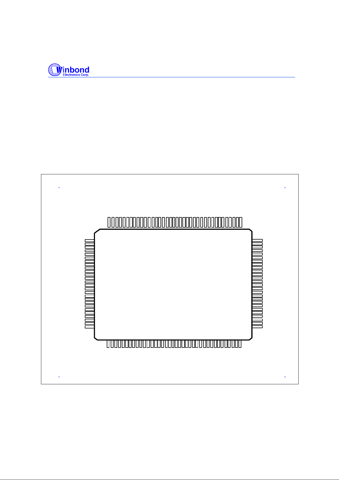
PIN CONFIGURATION FOR 626F
TC
BALE
IRQ3
IRQ4
DACK2#
SBHE#
IRQ5
GND
IRQ6
IRQ7
REFRESH#
SYSCLK
DACK1#
DRQ1
IOR#
DACK3#
DRQ3
VCC5
IOW#
LPC TO ISA BRIDGE SET
W83626F/W83626D
PRELIMINARY
SD0
SD1
SD2
VCC5
SD3
SD5
SD4
SD6
SD7
IOCHCK#
IRQ9
OWS#
GND
SMEMW#
DRQ2
SMEMR#
RSTDRV
GPIO6/RTCCS#
GPIO7/IOHCS#
MEMR#
MEMW#
MASTER#/RTCEN
DACK7#
DACK6#/HEFRAS
LA23
LA22
VCC5
LA21
LA20
LA19
LA18
GND
LA17
SD8
SD9
SD10
SD11
SD12
SD13
VCC5
SD14
SD15
DRQ7
GND
DRQ6
1
0101099
2 1
103
104
105
106
107
108
109
110
111
112
113
114
115
116
117
118
119
120
121
122
123
124
125
126
127
128
1 2 3 4 5 6 7 8 9
DRQ5
989
0
DRQ0
DACK5#
DACK0#
969594939
7
9
1
2
9089888
868
7
8
4838281
5
8
07978777675
W83626F
LPC to ISA
101112131415161718192021222324252627282930313233343536373
GND
LAD3
LAD2
LAD1
PCIRST#
LAD0
VCC3
LDRQ#
PCICLK
SERIRQ
AVCC3
14.318M
PWRDN#
14MOUT1
VCC5
IRQ14
IRQ15
IRQ12
IRQ11
IRQ10
LFRAM#
IOCS16#
MEMCS16#
747
7
7
1
2
3
SA0
AGND
24.576M
14MOUT2
706
SA1
9
SA2
6
867
SA3
6
6
6
5
64
63
62
61
60
59
58
57
56
55
54
53
52
51
50
49
48
47
46
45
44
43
42
41
40
39
8
SA4
ROMCS#
GPIO0/IRQ1
80PCS#/KBEN#
GPIO5/IRQ8
GPIO4/PLED
GPIO3/IRQIN
IOCHRDY
GND
AEN
SA19
SA18
SA17
VCC5
SA16
SA15
SA14
SA13
GND
SA12
SA11
SA10
SA9
VCC5
SA8
SA7
SA6
SA5
GPIO2/MCCS#
GPIO1/KBCS#
Publication Release Date: Feb 2000
- 3 - Revision 0.50
Page 6
1. PIN DESCRIPTION
I/O
- TTL level bi-directional pin with 12 m A source-sink capability
12t
I/O
- TTL level bi-directional pin with 24 m A source-sink capability
24t
I/O
- 3.3V TTL level bi-directional pin with 12 m A source-sink capability
12tp3
I/O
- 3.3V TTL level bi-directional pin with 24 m A source-sink capability
24tp3
I/O
- TTL level bi-directional pin open drain output with 12 m A sink capability
D12t
I/O
- TTL level bi-directional pin with 24 m A source-sink capability
24t
OUT12 - TTL level output pin with 12 m A source-sink capability
OUT24 - TTL level output pin with 24 m A source-sink capability
O
- 3.3V TTL level output pin with 12 m A source-sink capability
12p3
O
- 3.3V TTL level output pin with 24 m A source-sink capability
24p3
O
- Open-drain output pin with 12 m A sink capability
D12
O
- Open-drain output pin with 24 m A sink capability
D24
INcs - CMOS level Schmitt-trigger input pin
INt - TTL level input pin
INtd - TTL level input pin with internal pull down resistor
INtu - TTL level input pin with internal pull up resistor
INts - TTL level Schmitt-trigger input pin
IN
- 3.3V TTL level Schmitt-trigger input pin
tsp3
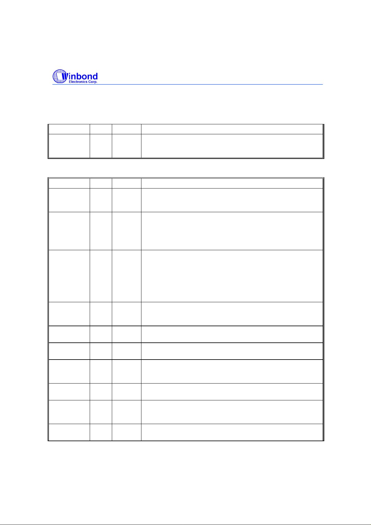
W83626F PIN DESCRIPTION
LPC Interface
LPC TO ISA BRIDGE SET
W83626F/W83626D
PRELIMINARY
SYMBOL PIN I/O FUNCTION
LAD[3:0] 16-19 I/O
These signal lines communicate address, control and data
12tp3
information over the LPC bus between a host and a peripheral.
LFRAME# 13 IN
PCICLK
21
PCIRST# 14 IN
SERIRQ 23 I/O
LDRQ# 22 O
Indicates start of a new cycle or termination of a broken cycle.
tsp3
PCICLK provides timing for all transactions on the LPC bus. All
INt
tsp3
D12t
12tp3
LPC signals are sampled on the rising edge of PCICLK, and all
timing parameters are defined with respect to this edge.
Reset signal. It can connect to PCIRST# signal on the host.
Serial IRQ Input/Output.
Encoded DMA Request signal.
Publication Release Date: Feb 2000
- 4 - Revision 0.50
Page 7
LPC TO ISA BRIDGE SET
W83626F/W83626D
PRELIMINARY
LPC Interface, continued
SYMBOL PIN I/O FUNCTION
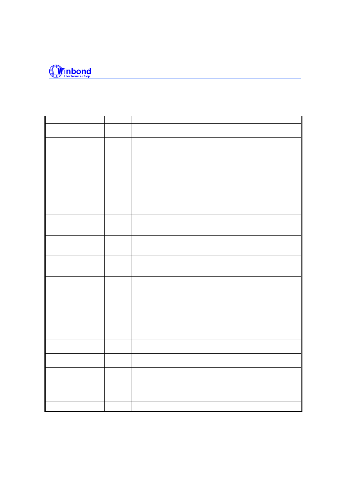
PWRDN# 24 INtu Power Down. The signal is active low according to CR 44 Bit 7and
wake-up enable by hardware setting. There are eight different
power-down states (Power down Mode 3).
ISA Interface Signals
SYMBOL PIN I/O FUNCTION
SA[19:17] 58-56 OUT24 System Address Bus. These are the upper address lines that
define the ISA’s byte granular address space (up to 1 M byte).
SA[19:17] are at an unknown state upon PCIRST#.
SA[16:0] 54-51
SD[15:0] 122-1
AEN 59 OUT24 Address Enable. AEN is asserted during DMA cycles. This signal
IOR# 86 OUT24 I/O Read. IOR# is the command to an ISA I/O slave device that the
IOW# 84 OUT24 I/O Write. IOW# is the command to an ISA I/O slave device that
IOCHRDY
SYSCLK 92 OUT24 ISA System Clock. SYSCLK is the reference clock for the ISA
RSTDRV
IOCS16# 11 INt 16-bit I/O Chip Select. This signal is driven by I/O devices on the
49-46
44-41
35-31
21
119-1
14
75-71
69-67
61
77 OUT24
OUT24 System Address Bus. These are the bi-directional lower address
lines that define the ISA’s byte granular address space (up to 1 M
byte). SA[16:0] are at an unknown state upon PCIRST#.
OUT24 System Data. SD[15:0] provide the 16-bit data path for devices
residing on the ISA Bus. The W83626F tri-states SD[15:0] during
PCIRST#.
is also driven high during W83626F initiated refresh cycles. AEN is
driven low upon PCIRST#.
slave may drive data on to the ISA data bus (SD[15:0]).
the slave may latch data from the ISA data bus (SD[15:0]).
INt
I/O Channel Ready. Resources on the ISA Bus negate IOCHRDY
to indicate that additional time (wait states) is required to complete
the cycle.
bus. The SYSCLK is generated by dividing PCICLK by 3 or 4.
Reset Drive. W83628F asserts RSTDRV to reset devices that
reside on the ISA Bus. The W83628F asserts this signal while the
PCIRST# is asserted.
ISA Bus to indicate that they support 16-bit I/O bus cycles.
Publication Release Date: Feb 2000
- 5 - Revision 0.50
Page 8
LPC TO ISA BRIDGE SET
W83626F/W83626D
PRELIMINARY
ISA Interface Signals , continued
SYMBOL PIN I/O FUNCTION
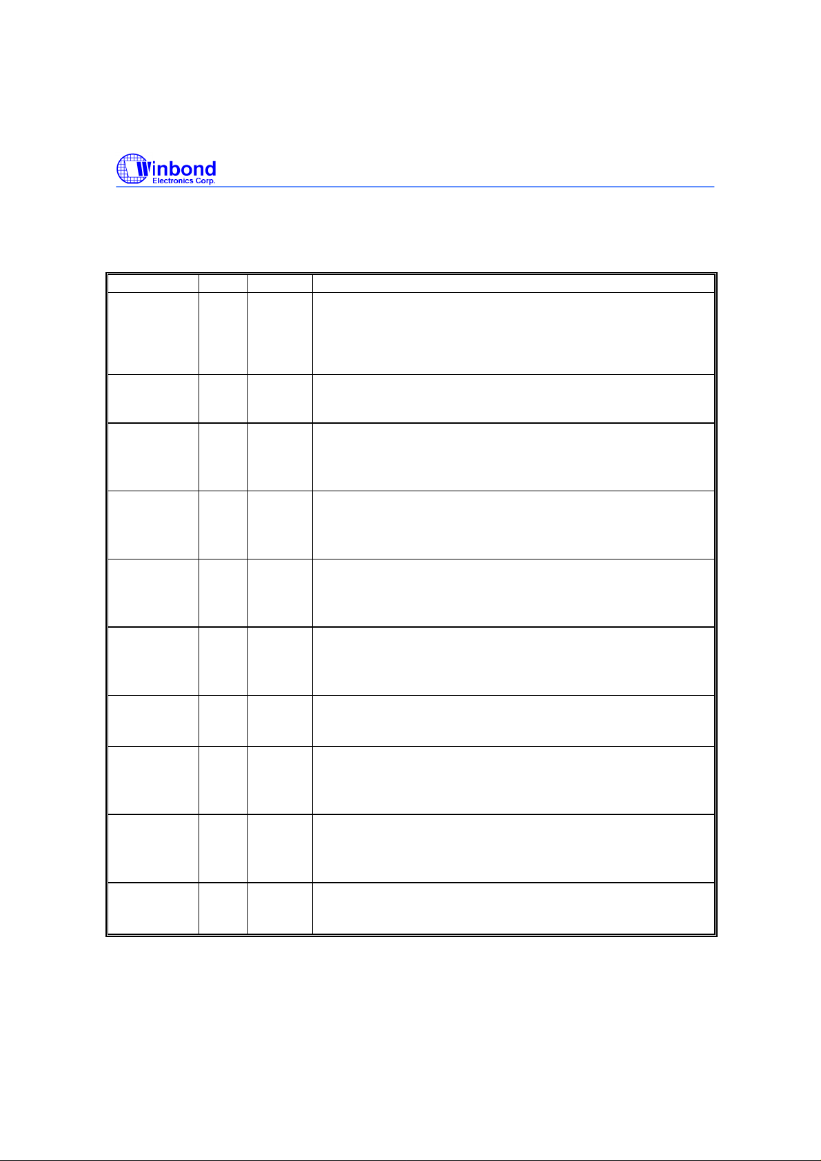
MEMCS16# 12 INt
IOCHCK# 76 INt I/O Channel Check. IOCHK# can be driven by any resource on
OWS# 81 INt
LA[23:17]
SMEMW# 82 OUT24
SMEMR# 83 OUT24
REFRESH# 91 OUT24
BALE 101 OUT24
SBHE# 102 OUT24 System Byte High Enable. SBHE# asserted indicates that a byte
MEMR# 112 OUT24
MEMW# 113 OUT24
MASTER#
RTCEN#
IRQ3 98
103-1
04
106-1
09
111
123 INt
OUT24
INt Parallel Interrupt Requested Input 3.
Memory Chip Select 16. MEMCS16# asserted indicates that the
memory slave supports 16-bit accesses.
the ISA bus during on detection of an error.
Zero Wait States. An ISA slave asserts ZEROWS# after its
address and command signals have been decoded to indicate that
the current cycle can be executed as an ISA zero wait state cycle.
ZEROWS# has no effect during 16-bit I/O cycles.
Unlatched Address. The LA[23:17] address lines are
bi-directional. These address lines allow accesses to physical
memory on the ISA Bus up to 16 Mbytes. LA[23:17] are outputs
when the W83628F owns the ISA Bus.
Standard Memory Write. SMEMW# asserted indicates the
current ISA bus cycle is a memory write cycle to an address below
1 Mbyte.
Standard Memory Read. SMEMR# asserted indicates the
current ISA bus cycle is a memory read cycle to an address below
1 Mbyte.
Refresh. REFRESH# asserted indicates that a refresh cycle is in
progress, or that an ISA master is requesting W83626F to
generate a refresh cycle. Upon PCIRST#, this signal is tri-stated.
Bus Address Latch Enable. BALE is an active high signal
asserted by the W83626F to indicate that the address (SA[19:0],
LA[23:17]) and SBHE# signal lines are valid.
The LA[23:17] address lines are latched on the trailing edge of
BALE. BALE remains asserted throughout DMA and ISA master
cycles. BALE is driven low upon PCIRST#.
is being transferred on the upper byte (SD[15:8]) of the data bus.
SBHE# is at an unknown state upon PCIRST#.
Memory Read. MEMR# asserted indicates the current ISA bus
cycle is a memory read.
Memory Write. MEMW# asserted indicates the current ISA bus
cycle is a memory write.
MASTER#. This signal is used with a DREQ line by an ISA master
to gain control of the ISA Bus.
RTC Function Enable.The pin applies a pull-down resistor (4.7K
ohm) to enable RTC functions ( RTCCS#,and IRQ8)
Publication Release Date: Feb 2000
- 6 - Revision 0.50
Page 9

LPC TO ISA BRIDGE SET
W83626F/W83626D
PRELIMINARY
ISA Interface Signals , continued
SYMBOL PIN I/O FUNCTION
IRQ4 97
IRQ5 96
IRQ6 94
IRQ7 93
IRQ9 78
IRQ10 10
IRQ11 9
IRQ12 8
IRQ14 6
IRQ15 7
DRQ0 3
DRQ1 90
DRQ2 79
DRQ3 88
DRQ5 1
DRQ6 127
DRQ7 124
DACK0# 4 OUT24 DMA Acknowledge 0. The DACK# signal indicates that either a
DACK1# 89 OUT24 DMA Acknowledge 1.
DACK2# 99 OUT24 DMA Acknowledge 2.
DACK3# 87 OUT24 DMA Acknowledge 3.
DACK5# 2 OUT24 DMA Acknowledge 5.
DACK6#
HERFRA
DACK7# 126 OUT24 DMA Acknowledge 7.
TC 100 OUT24 Terminal Count. The W83628F asserts TC to DMA slaves as a
127 I/O
INt Parallel Interrupt Requested Input 4.
INt Parallel Interrupt Requested Input 5.
INt Parallel Interrupt Requested Input 6.
INt Parallel Interrupt Requested Input 7.
INt Parallel Interrupt Requested Input 9.
INt Parallel Interrupt Requested Input 10.
INt Parallel Interrupt Requested Input 11.
INt Parallel Interrupt Requested Input 12.
INt Parallel Interrupt Requested Input 14.
INt Parallel Interrupt Requested Input 15.
INt
INt
INt
INt
INt
INt
INt
D24t
DMA Request 0. The DREQ signal indicates that either a slave
DMA device is requesting DMA services, or an ISA bus master is
requesting use of the ISA bus.
DMA Request 1.
DMA Request 2.
DMA Request 3.
DMA Request 5.
DMA Request 6.
DMA Request 7.
DMA channel or an ISA bus master has been granted the ISA bus.
DMA Acknowledge 6.
During power-on reset,this is pulled-hi internally(Select 4Eh) and
is defined as HEFRAS which provides the power-on value for
CR3 bit4 .A 4.7k ohm is recommended if intends to pull down
.(Select 2Eh)
terminal count indicator.
Publication Release Date: Feb 2000
- 7 - Revision 0.50
Page 10
LPC TO ISA BRIDGE SET
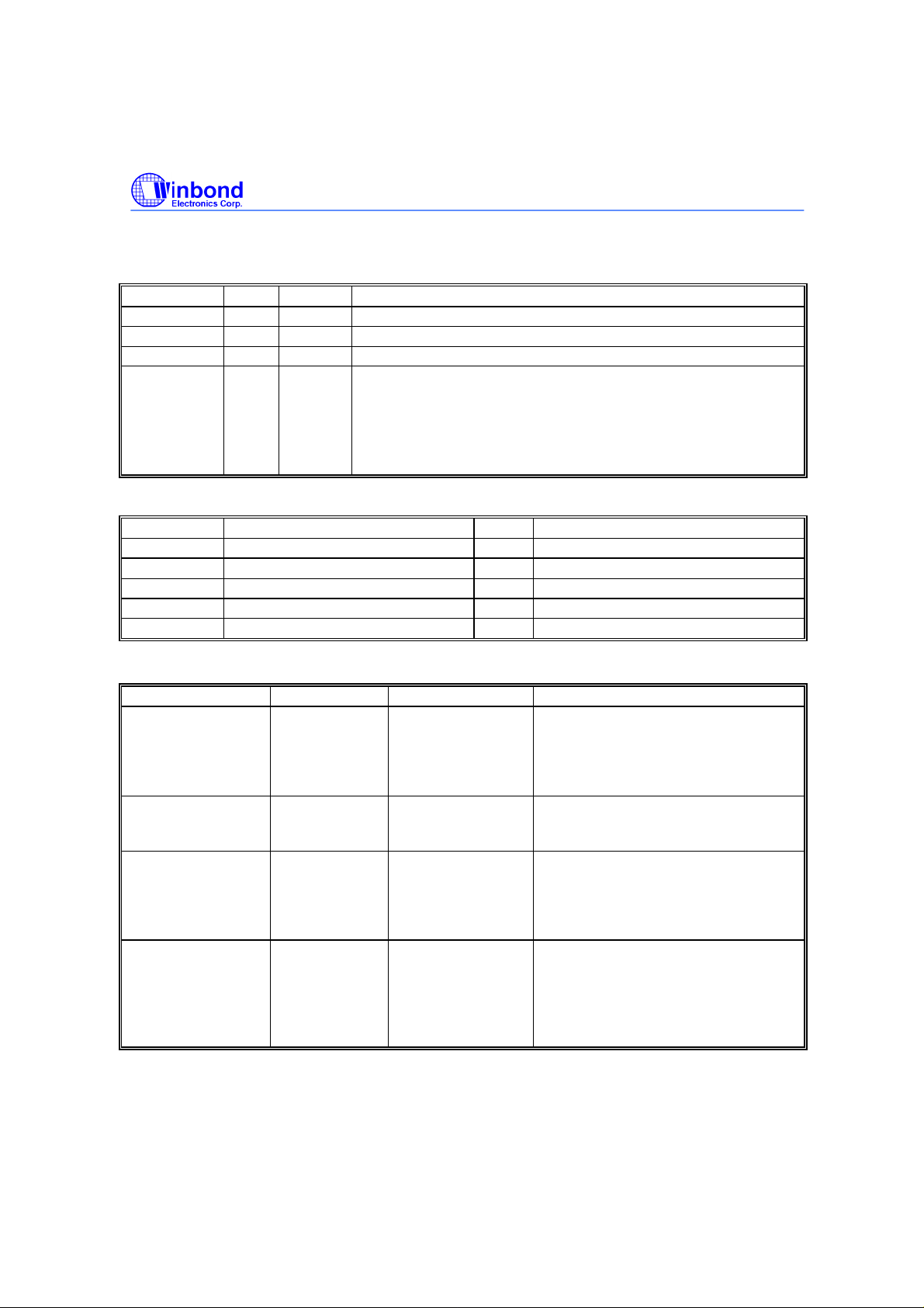
K/B , GPIO AND 80h PCS# Function
SYMBOL PIN I/O FUNCTION
80PCS#
KBEN#
ROMCS# 37 I/O
GPIO0
IRQ1
GPIO1
KBCS#
GPIO2
MCCS#
GPIO3
IRQIN
GPIO4
PLED
GPIO5
IRQ8
GPIO6
RTCCS#
GPIO7
IOHCS#
36 I/O
38 I/O
39 I/O
40 I/O
62 I/O
63 I/O
64 I/O
65 I/O
66 I/O
80h PORT Chip Select.(Default)
D12t
K/B Functions Enable. During power-on reset this pin is weak
pulled-up internally. The pin applied a pull-down resistor (4.7K
ohm) to enable K/B functions. (IRQ1,KBCS#,and MCCS#)
ROMCS#, this pin enable positive decoder of BIOS address range
D12t
D12t
D12t
D12t
D12t
D12t
D12t
D12t
[depend on CR03 ,bit 1 or external weak pulled-up during PCIRST
is asserted] .
General purpose I/O pin 0.
Parallel Interrupt Requested Input 1. This interrupt request is used
for specific K/B functions.
General purpose I/O pin 1.
12t
Decode the address 60h and 64h to output chip selected signal.
Enable by KBEN# power-on setting.
General purpose I/O pin 2.
Decode the address 62h and 66h to output chip selected signal
Enable by KBEN# power-on setting
General purpose I/O pin 3.
Programmable parallel IRQ input transfers to serial IRQ
Enable by KBEN# power-on setting
General purpose I/O pin 4.
Power LED output, this signal is low after system reset.
General purpose I/O pin 5.
Parallel Interrupt Requested Input 8. This interrupt request is used
for specific RTC functions. Enable by RTCEN# power-on setting
General purpose I/O pin 6.
Decode the address 70h and 71h to output chip selected signal
Enable by RTCEN# power-on setting
General purpose I/O pin 7.
Decode SA[15-11] are all 0 and setting by CR04 Bit 6.
W83626F/W83626D
PRELIMINARY
Publication Release Date: Feb 2000
- 8 - Revision 0.50
Page 11
LPC TO ISA BRIDGE SET
64 and 65 will do IRQ8 and RTCCS#
W83626F/W83626D
Clock Buffer and Generator
SYMBOL PIN I/O FUNCTION
14.318M 26 INt Main 14.318 MHz Clock Input.
14MOUT 1 27 OUT
14MOUT 2 28 OUT
24.576M
25.000M
Power Signals
SYMBOL PIN I/O FUNCTION
VCC5 5, 45, 55, 70, 85, 105, 120, PWR Digital 5V Supply.
VCC3 20 PWR Digital 3.3V Supply.
GND 15, 50, 60, 80, 95, 110, 125 PWR Digital Ground.
AVCC3 25 PWR Analog 3.3V Supply.
AGND 30 PWR Analog Ground.
Power-on strapping Signals
SYMBOL PIN I/O FUNCTION
80PCS#/KBEN# 36 I/O
ROMCS# 37 I/O
MASTER/RTCEN# 123 INt
29 OUT
14.318 MHz Buffer Output 1.
12t
14.318 MHz Buffer Output 2.
12t
This pin is weak pull-up during 3 VDD ramp-up period. The default
12t
setting is 24.576 MHz and selected 25.000 MHz by external
pull-down with 4.7K ohm (recommended) during power ramp-up
period.
24.576 MHz Clock Output for Audio Codec or selected 25.000
MHz Clock Output for LAN on board solution.
D12t
D12t
Power-on strapping with
pulled-down register will enable
K/B and mouse functions. When it
is set, pin 38 , 39 and 40 will do
IRQ1, KBCS# and MCCS# signals.
If there is a boot-ROM (BIOS) ,the
signal must power-on with a weak
pulled-high register.
Power-on strapping with
pulled-down register will enable
RTC functions. When it is set, pin
PRELIMINARY
DACK6#/HEFRAS 128 I/O
signals.
D24t
- 9 - Revision 0.50
Set this function will change the
port that is used to access
configuration-registers . Default
setting is 4Eh ,but by power-on
strapping with a pulled-down
register change to 2Eh.
Publication Release Date: Feb 2000
Page 12

LPC TO ISA BRIDGE SET
W83626F/W83626D
PRELIMINARY
CONFIGURATION REGISTER
1 Chip (Global) Control Register
Enable the following configuration registers by writing 26h to the location 4Eh twice.
Change the location to 2Eh by setting bit4 of CR03 or power-on strapping with a
pulled-down register on pin 128 .
CR03 (ROM Decoder Register, Default , 100011s0b)
Bit 7-5 Reserved.
Bit4 Configure Address and Value
= 0 Write 26h to the location 4E twice. (4Eh and 4Fh are index and data port)
= 1 Write 26h to the location 2E twice(By DACK6 power-on setting with
weak pull-down resistor).(The pair are 2Eh and 2Fh)
Bit 3-2
= 00 1MB BIOS ROM positive decode.
= 01 2MB BIOS ROM positive decode.
= 10 4MB BIOS ROM positive decode.
= 11 8MB BIOS ROM positive decode. (Default setting)
Bit 1
= 0 Disable BIOS ROM decoder. (Default setting)
=1 Enable BIOS ROM decoder.
Bit 0 BIOS Protected Mode.
=0 BIOS Writed Disable. (Default setting)
=1 BIOS Writed Enable.
This bit set to “ 1 ” for updated BIOS used allow Memory R/W to the range
of BIOS decoded. This bit is always set to “ 0 “ after reset.
BIOS Decode Range of High Memory.
BIOS ROM decoder Enable.
Publication Release Date: Feb 2000
- 10 - Revision 0.50
Page 13

LPC TO ISA BRIDGE SET
W83626F/W83626D
PRELIMINARY
CR04 (GPIO Status Register , Default 0ss00sssb)
If the GPIO is selected GPIO function, it will be controlled by CR10,13,14,15,and 16.The pins were
set non-GPIO functions by power-on setting pin or software programmed.
Bit 7(GPIO7) : = 1 Signal used as IOHCS# (Set by software only)
= 0 Signal used as GPIO function (Default)
Bit 6 (GPIO6): = 1 Signal used as RTCCS# (Set by pin123 RTCEN# )
= 0 Signal used as GPIO function (Default)
Bit 5 (GPIO5): = 1 Signal used as IRQ8 (Set by Pin 123 RTCEN# )
= 0 Signal used as GPIO function (Default)
Bit 4 (GPIO4): = 1 Signal used as PLED ( Set by software only and programmed by CR CR17 bit [5,4])
= 0 Signal used as GPIO function . (Default)
Bit 3 (GPIO3): = 1 Signal used as IRQIN (depended on CR17 bit[3..0])
= 0 Signal used as GPIO function (Default)
Bit 2 (GPIO2): = 1 Signal used as MCCS# (decode address 62h and 66h )
by Pin 36 KBEN# power-on setting
= 0 Signal used as GPIO function (Default)
Bit 1 (GPIO1): = 1 Signal used as KBCS# (decode address 60h and 64h)
by Pin 36 KBEN# power-on setting
= 0 Signal used as GPIO (Default)
Bit 0 (GPIO0): = 1 Signal used as IRQ1 by Pin 36 KBEN# power-on setting
= 0 Signal used as GPIO (Default)
CR05 (System Clock Register , Default 0x4D)
Publication Release Date: Feb 2000
- 11 - Revision 0.50
Page 14

LPC TO ISA BRIDGE SET
W83626F/W83626D
PRELIMINARY
Bit 7 SYSCLK Divider.
= 0 SYSCLK is equal to PCICLK divided by 4.
= 1 SYSCLK is equal to PCICLK divided by 3.
Bit 6 8-bit I/O Recovery Enable
= 0 Disable bit [5:3] setting and uses 3.5 SYSCLKs for 8 bit I/O recovery time.
= 1 Enable bit [5:3] setting.
Bit 5:3 8-bit I/O Recovery Times .
When bit 6= 1 , these 3 bits field define the additional number of SYSCLKs added
to standard 3.5 SYSCLK recovery time for 8 bit I/O
= 000 0 SYSCLK
= 001 1 SYSCLK
= 010 2 SYSCLKs
= 011 3 SYSCLKs
= 100 4 SYSCLKs
= 101 5 SYSCLKs
= 110 6 SYSCLKs
= 111 7 SYSCLKs
Bit 2 = 0 Ignore bits [1:0] setting and uses 3.5 SYSCLKs for 16-bit I/O recovery
time.
= 1 The 16-bit I/O recovery time is decided by bits 1:0.
Bit 1:0 16-bit I/O Recovery Times.
When bit 2 = 1 , this 2-bit field defines the additional number of SYSCLKs added
to standard 3.5 SYSCLK recovery time for 16 bit I/O
= 01 1 SYSCLK
= 10 2 SYSCLKs
= 11 3 SYSCLKs
= 00 4 SYSCLKs
CR10 (GPIO0-GPIO7 Function Enable Register, Default 0x00)
Bit 7 - 1: Reserved.
Publication Release Date: Feb 2000
- 12 - Revision 0.50
Page 15

LPC TO ISA BRIDGE SET
W83626F/W83626D
PRELIMINARY
Bit 0: GPIO Function Activity.
= 1 All GPIO functions are activated . All registers (CR 11,12,13,14,15,16)
about GPIO function will be set default value .
= 0 All GPIO functions are inactive except the signals by power-on setting.
If any one of CR04 bit [7..0] was set non-GPIO function,the bit just affect
which was set GPIO function .
CR11, CR12 (Reserved Register For GPIO Control Without Configure Mode Entry )
The register is programmable when the bit 0 of CR10 is set to “ 1 “ and affected by
the settings of CR14 ( I/O Selectioin ) and CR16 ( Inversion ).
User defines port address to control GPIO functions. To control GPIO state without entry
configure mode. SA [0..7] can be defined on the bit [0..7] of CR11 and SA [8..15] on the bit [
0..7] of CR12.
For example:
Define address 50h in CR11 and 01h in CR12 after reset.
bit 0= -GPIO0 (=0 low state,
=1 Hi state )
bit 1=-GPIO1 (=0 low state
=1 Hi state)
,bit 2=GPIO2,.........,bit 7=GPIO7 the same definition as bit 0.
Set CR14 to “ 00h “ (output port) and CR16 to “ 00h “ (incoming/outgoing)
-o 150 aa ------(10101010) b indicated GP7,GP5,GP3 and GP1 are Hi state.
-o 150 55 ------(01010101) b indicated GP6,GP4,GP2,and GP0 are Hi state.
- i 150 ------show all states of GPIO[7..0]
CR13 (GPIO0-GPIO7 Address Decoder Rester, Default 0x00 )
The register is programmable when the bit 0 of CR10 is set to “ 1 “.
Bit 7: Address Decoder 2
=1 Enable address decoder .Generate a CS# signal to GPIO port which
decided by bit[6..4] ,the specify address in CR34 and CR35 and mask
range in CR 33.
=0 Disable address decoder.
Publication Release Date: Feb 2000
- 13 - Revision 0.50
Page 16

LPC TO ISA BRIDGE SET
W83626F/W83626D
PRELIMINARY
Bit 6 -Bit 4 : Address Decoder 2 Output Selection.
Define which GP port as address decoder depended on CR33,CR34 and CR35.
= 000 Selected GPIO 0 as CS# output
= 001 Selected GPIO 1 as CS# output
= 010 Selected GPIO 2 as CS# output
= 011 Selected GPIO 3 as CS# output
= 100 Selected GPIO 4 as CS# output
= 101 Selected GPIO 5 as CS# output
= 110 Selected GPIO 6 as CS# output
= 111 Selected GPIO 7 as CS# output
Bit 3: Address Decoder 1
=1 Enable address decoder . Generate a CS# signal to GPIO port which
decided by bit[6..4] ,the specify address in CR31 and CR32 and mask
range in CR 30.
=0 Disable address decoder.
Bit 2 -Bit 0 : Address Decoder 1 Output Selection.
Define which GP port as address decoder depend on CR30,CR31 and CR32.
= 000 Selected GPIO 0 as CS# output
= 001 Selected GPIO 1 as CS# output
= 010 Selected GPIO 2 as CS# output
= 011 Selected GPIO 3 as CS# output
= 100 Selected GPIO 4 as CS# output
= 101 Selected GPIO 5 as CS# output
= 110 Selected GPIO 6 as CS# output
= 111 Selected GPIO 7 as CS# output
CR14 (GPI0-GPIO7 I/O Selection Register, Default 0xFF)
The register is programmable when the bit 0 of CR10 is set to “ 1 “.
Bit [7..0] are corresponding with GPIO [7..0] .
When set to a '1', respective GPIO port is programmed as an input port.
When set to a '0', respective GPIO port is programmed as an output port.
Publication Release Date: Feb 2000
- 14 - Revision 0.50
Page 17

LPC TO ISA BRIDGE SET
W83626F/W83626D
PRELIMINARY
CR15 (GPIO0-GPIO7 Data Register, Default 0x00)
The register is programmable when the bit 0 of CR10 is set to “ 1 “.
Bit [7..0] are corresponding with GPIO [7..0] .
If a port is programmed to be an output port, then its respective bit can be read/written.
If a port is programmed to be an input port, then its respective bit can only be read.
CR16 (GPIO0-GPIO7 Inversion Register, Default 0x00)
The register is programmable when the bit 0 of CR10 is set to “ 1 “.
Bit [7..0] are corresponding with GPIO [7..0] .
When set to a '1', the incoming/outgoing port value is inverted.
When set to a '0', the incoming/outgoing port value is the same as in data register.
CR17 (Power LED & IRQIN Control Register, Default 0x00)
Bit 7 -6:Reserved
Bit 5 -4: =00 Power LED pin is tri-stated.
=01 Power LED pin is driven low.
=10 Power LED pin is a 1Hz toggle pulse with 50 duty cycle.
=11 Power LED pin is a 1/4 Hz toggle pulse with 50 duty cycle.
Bit 3 - 0: These bits select IRQ resource for IRQIN. Four bits transfer the decimal value to octal
system. For example: Bit [3..0] = 1001b = 0x9h means IRQ 9 be selected.
Bit [3..0] = 1100b = 0xCh means IRQ12 be selected
CR20 ( Chip ID Register 1, Default 0x62)
Bit 7 - 0: DEVIDB7 - DEBIDB0 --> Device ID Bit 7 - Bit 0 = 0x 62(read only).
CR21 (Chip ID Register 2 ,
Bit 7 - 0: DEVREVB7 - DEBREVB0 --> Device Rev Bit 7 - Bit 0 = 0x61(read only).
Default 0x6x)
Publication Release Date: Feb 2000
- 15 - Revision 0.50
Page 18

LPC TO ISA BRIDGE SET
W83626F/W83626D
PRELIMINARY
Bit [3..0] indicate the version of the chip.
CR30 (Mask Range of Address Decoder 1 Register, Default 0x00)
This register is used to mask address bits (A7~A0) for specify address decoder, if the corresponding bit
of this register is set to a 1, the corresponding address bit(A7~A0) is ignore by the specify address
decoder.
For example: If the decoding range is 0x3F8 ~ 0x3FF,you can set 0x3F8 to CR 31, 32 and 07h to
CR30 .
CR31, 32 (Address Decoder 1 Specification Register ,
This register contains the address for specify decoder.
CR 31 Bit [7..0] are used to define low byte of specity address.
CR 32 Bit [7..0] are used to define high byte of specify address.
For example: Decoding address was set to be 0x3F5h and write F5h to CR 31 and 03h to CR 32 .
CR33 ((Mask Range of Address Decoder 2 Register, Default 0x00)
This register is used to mask address bits(A7~A0) for specify address decoder , if the corresponding bit
of this register is set to a 1, the corresponding address bit(A7~A0) is ignore by the specify address
decoder .
For example: If the decoding range is 0x3F8 ~ 0x3FF,you can set 0x3F8 to CR 34, 35 and 07h to
CR33 .
Default 0x00)
CR34, 35 Address Decoder 2 Specification Register , Default 0x00)
This register contains the address for specify decoder.
CR 34 Bit [7..0] are used to define low byte of specity address.
CR 35 Bit [7..0] are used to define high byte of specify address.
For example: Decoding address was set to be 0x3F5h and write F5h to CR34 and 03h to CR35.
This register contains the address for specify decoder.
Publication Release Date: Feb 2000
- 16 - Revision 0.50
Page 19
LPC TO ISA BRIDGE SET
W83626F/W83626D
PRELIMINARY
CR40 (Clock controllable Register , Default 0x00)
This register is used to enable clock power-down state of the chip. It will shut down 14.318MHz.
Bit 7 -1: Reserved.
Bit 0 : =1 Power down mode.When entry power down mode , clock output will be turn off.
=0 Normal used.
CR41 (Clock tested Register , :Reserved for Winbond internal test)
CR42 (Tristate controllable Register(Power-down Mode1) , Default 0x1B)
Bit 7 : REFRESH Cycles Tristated.
Bit 6 : SYSCLK Output Tristated.
Bit 5 : Address Signals Tristated Enable.
Bit 4 - 0 : Defined tristated address signals range.(See Table 1)
For example:
Define address Bit[4..0] = 0x10h
SA [19..16] and LA [23..17] signals will be tristated.
Table 1
Set value(Hex) Tri_state range Workable
00 SA[19..0] and LA[23..17] None one
01 SA[19..1] and LA[23..17] SA[0]
02 SA[19..2] and LA[23..17] SA[1..0]
.
.
14 LA[23..17] SA[19..0]
Set value(Hex) Tri_state range Workable
.
.
.
.
. . .
Publication Release Date: Feb 2000
- 17 - Revision 0.50
Page 20

LPC TO ISA BRIDGE SET
W83626F/W83626D
PRELIMINARY
.
1A LA[23] SA[19..0] and LA[22..17]
1B None one SA[19..0] and LA[23..17]
.
.
CR43 (Tristate controllable Register(Power-down Mode2) ,Default 0x07)
The Fast mode is used to improve the performance of transferable interface, because some
applications will do fast transaction . To set the suitable bits to decide on specify range or all ISA cycles
will meet the requested I/O cycles.
Bit 7 : Reserved.
Bit 6 : = 1 Enable Fast mode by ADDRESS DECODER 2 and SYSCLK is depended on
the state of Bit 3 .
= 0 ADDRESS DECORDER 2 doesn’t affect Fast Mode and do original operation.
Bit 5 : = 1 Enable Fast mode by ADDRESS DECODER 1 and SYSCLK is depended on
the state of Bit 3.
= 0 ADDRESS DECORDER 1 doesn’t affect Fast Mode and do original operatio
Bit 4 : = 1 Enable Fast Mode of whole chip, whole ISA cycle of this bridge will be done
Fast Mode operation and SYSCLK is depended on the state of Bit 3.
= 0 Normal operation, just Bit 6 and Bit 5 can affect Fast Mode operation.
Bit 3 : = 1 SYSCLK is equal to PCICLK divided by 1 when decoding range is in Fast Mode.
= 0 SYSCLK is equal to PCICLK divided by 2 when decoding range is in Fast Mode.
Bit 2 : = 1 Disabled Memory cycles.
= 0 Normal used.
Bit 1 : = 1 Forced 16 bit cycles .
= 0 Normal used.
Bit 0 : = 1 8-bit data bus decode only. Only SD [7..0] signals are active.
Publication Release Date: Feb 2000
- 18 - Revision 0.50
Page 21

LPC TO ISA BRIDGE SET
W83626F/W83626D
PRELIMINARY
= 0 Normal used.
CR44 (Tristate controllable Register(Power-down Mode3) , Default 0x07)
Bit 7 : =1 Enable Power-down functions.(ISOLATE# was power-on setting.)
=0 Normal used.
Bit 6 : Reserved.
Bit 5 : =1 SA10 is set as mask (ignored) bit in ADDRESS DECODER 2. The function is used to improved
the performance of ECP mode of LPT. If the decoding range is 0x378-0x37F and 0x778-0x77F
,you can set this bit to 1 for Fast Mode operation.
= 0 Normal operation.
Bit 4 : =1 SA10 is set as mask (ignored) bit in ADDRESS DECODER 1. The function is used to improved
the performance of ECP mode of LPT. If the decoding range is 0x378-0x37F and 0x778-0x77F
,you can set this bit to 1 for Fast Mode operation.
= 0 Normal operation.
Bit 3 : SERIRQ POWER DOWN SELECT.
=1 When the chip is in power down mode, the SERIRQ block is inactive.
=0 When the chip is in power down mode, the SERIRQ block is active.
Bit 2 -0 : Set SYSCLK divided ratio.(2,4,8,16,32,64)
= 000 Disable Power-down Mode3.
= 001 SYSCLK divided by 2.
= 010 SYSCLK divided by 4.
= 010 SYSCLK divided by 4
= 011 SYSCLK divided by 8
= 100 SYSCLK divided by 16
= 101 SYSCLK divided by 32
= 110 SYSCLK divided by 64
= 111 LPC I/F,all clocks and signals will be tristated.
Publication Release Date: Feb 2000
- 19 - Revision 0.50
Page 22

LPC TO ISA BRIDGE SET
W83626F/W83626D
PRELIMINARY
CR45 (Wake-Up Event Register, Default 0x01)
Bit 7 :=0 Normal used.
=1 Wake up from power-down mode by IRQ 7 occurred.
Bit 6 : =0 Normal used.
=1 Wake up from power-down mode by IRQ 6 occurred.
Bit 5 : =0 Normal used.
=1 Wake up from power-down mode by IRQ 5 occurred.
Bit 4 : =0 Normal used.
=1 Wake up from power-down mode by IRQ 4 occurred .
Bit 3 : =0 Normal used.
=1 Wake up from power-down mode by IRQ 3 occurred.
Bit 2 :Reserved.
Bit 1 : =0 Normal used.
=1 Wake up from power-down mode by IRQ 1 occurred.
Bit 0 : =0 Normal used.
=1 Wake up from power-down mode by rising edge of ISOLATE# signal occurred.
CR46(Wake-Up Event Register, Default 0x00)
Bit 7 -5:Reserved
Bit 4 : =0 Normal used.
=1 Wake up from power-down mode by IRQ 12 occurred .
Bit 3 : =0 Normal used.
=1 Wake up from power-down mode by IRQ 11 occurred.
Publication Release Date: Feb 2000
- 20 - Revision 0.50
Page 23

LPC TO ISA BRIDGE SET
W83626F/W83626D
PRELIMINARY
Bit 2 : =0 Normal used.
=1 Wake up from power-down mode by IRQ 10 occurred.
Bit 1 : =0 Normal used.
=1 Wake up from power-down mode by IRQ 9 occurred.
Bit 0 : =0 Normal used.
=1 Wake up from power-down mode by IRQ 8 occurred.
CR48 (DMA CYCLES FAST MODE SELECT, Default 0x00) (Write only)
The Fast mode is used to improve the performance of transferable interface, because some
applications will do fast transaction . To set the suitable bits to decide on specify range or all ISA cycles
will meet the requested DMA cycles.
Bit 7 : = 0 Normal used.
= 1 The DMA cycles of channel 7 is in fast mode.
Bit 6 : = 0 Normal used.
= 1 The DMA cycles of channel 6 is in fast mode.
Bit 5 : = 0 Normal used.
= 1 The DMA cycles of channel 5 is in fast mode.
Bit 4 : Reserved.
Bit 3 : = 0 Normal used.
= 1 The DMA cycles of channel 3 is in fast mode.
Bit 2 : = 0 Normal used.
= 1 The DMA cycles of channel 2 is in fast mode.
Bit 1 : = 0 Normal used.
= 1 The DMA cycles of channel 1 is in fast mode.
Publication Release Date: Feb 2000
- 21 - Revision 0.50
Page 24

Bit 0 : = 0 Normal used.
= 1 The DMA cycles of channel 0 is in fast mode.
LPC TO ISA BRIDGE SET
W83626F/W83626D
PRELIMINARY
Publication Release Date: Feb 2000
- 22 - Revision 0.50
Page 25

LPC TO ISA BRIDGE SET
W83626F/W83626D
PRELIMINARY
REVISION NOTICES.
a. 4/16/1999 modified page 2, 3 to correct wrong typewrite and changed to Rev 0.02.
b. 5/18/1999 modified page 1,3 to define K/B functions , 80portCS# and IRQINX.Changed
ROMCS#from pin 39 to pin37.page 8,added and modified the function description and
changed to Rev0.03
c.5/27/1999 modified page 7 to add power-on setting function in DACK6# for entry port of
configure mode(HERFRA). In page 6,Master# was added RTCEN power-on setting function.
In page 8,80PCS# was added KBEN power-on setting function and GPIO 5 added a new
function IRQ8,GPIO6 added RTCCS#,and GPIO7 added IOHCS#.Rev 0.04 changed.
d.5/31/1999 Added Power-Down functin in islate#( page 5)and PLED function in GPIO3(page 8)
IRQIN2 was removed and IRQIN1 modified to IRQIN.
e.6/8/1999 Renamed ISOLATE# to PWRDN# and corrected RTCCS# decode address
(71,72--> 70,71),
f. 6/9/1999 modified the function descriptioin of pin 29.Rev 0.05 changed.
g.7/9/1999 Combined configuration register and modified new schematic.Rev 0.06.
h.7/21/1999 Modified default value of CR and add ed some descriptions and corresponding table.
Rev 0.07.
i. 8/24/1999 Modified recommended circuit and register descriptions. Corrected power-on setting
description of signal ROMCS# . Rev 0.10.
j.10/08/1999 modified pin configuration ,pin62 and 63.Rev 0.11
k. 11/16/1999 Modified schematic circuit and added the function description of CR43 and CR44. Rev
0.12.
l. 02/20/2000 Add new pacake 100-LQFP (W83626D) dimention
Publication Release Date: Feb 2000
- 23 - Revision 0.50
Page 26
LPC TO ISA BRIDGE SET
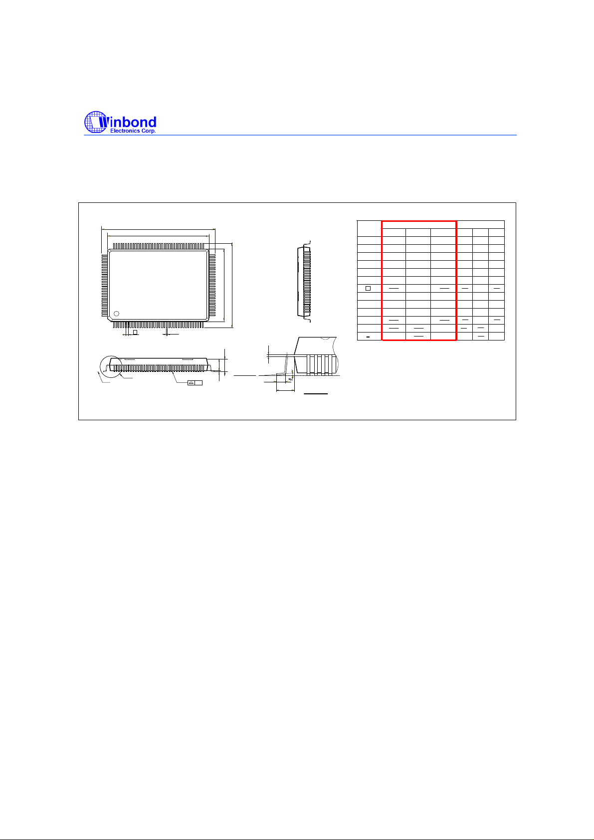
Package DIMENSIONS 1 for W83626F (128-pin PQFP)
W83626F/W83626D
PRELIMINARY
103
128
102
1
Seating Plane
e
See Detail F
H
E
E
65
64
Symbol
A
A
b
c
1
2
D
D
H
D
39
38
b
A
2
A
1
A
y
c
L
L
1
Detail F
E
e
D
H
H
E
L
L1
y
0
Note:
1.Dimension D & E do not include interlead
2.Dimension b does not include dambar
3.Controlling dimension : Millimeter
4.General appearance spec. should be based
5. PCB layout please use the "mm".
Dimension in mm
Min Nom Max
0.25
0.35 0.45
2.72
2.57
0.10
0.20
0.10
0.15
14.00
13.90
19.90 20.00 20.10
0.50
17.20
17.00
23.00 23.20
0.80
0.65
1.60
0
flash.
protrusion/intrusion
on final visual inspection spec.
.
2.87
0.30
0.20
14.10
17.40
23.40
0.95
0.08
7
Dimension in inch
MaxNomMin
0.010
0.014 0.018
0.113
0.107
0.101
0.004
0.004
0.547
0.783 0.787 0.791
0.669
0.905 0.913 0.921
0.025
0.012
0.008
0.008
0.006
0.555
0.551
0.020
0.685
0.677
0.037
0.031
0.063
0.003
0
7
Publication Release Date: Feb 2000
- 24 - Revision 0.50
Page 27
LPC TO ISA BRIDGE SET
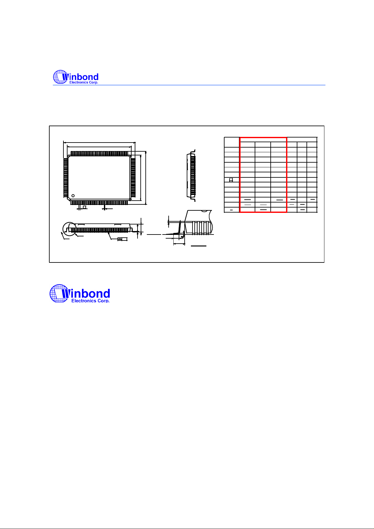
Package DIMENSIONS 2 for W83626D (128-pin LQFP)
W83626F/W83626D
PRELIMINARY
H
E
102
103
128
1 38
Seating Plane
E
e
See Detail F
Symbol
65
64
HD
D
39
b
A
2
A
1
A
y
c
L
L
1
Detail F
1
A
2
A
b
c
D
E
e
D
H
H
E
L
1
L
y
0
Note:
1.Dimension D & E do not include interlead
2.Dimension b does not include dambar
3.Controlling dimension : Millimeter
4.General appearance spec. should be based
5. PCB layout please use the "mm".
Dimension in mm
Min Nom Max
0.05 -----
1.40
1.35
0.13
0.16
0.10
-----
14.00
13.90
19.90 20.00 20.10
0.40 BSC
-----
16.00
-----
-----
----- 22.00
0.60
0.45
1.00
0
flash.
protrusion/intrusion
on final visual inspection spec.
.
14.10
-----
-----
-----
0.15
1.45
0.23
0.20
0.75
0.08
7
Dimension in inch
0
MaxNomMin
---- 0.006
0.057
0.055
0.009
0.006
0.008
-----
0.555
0.551
-----
0.016
-----
0.630
0.030
0.024
0.039
0.003
0.002
0.053
0.005
0.004
0.547
0.783 0.787 0.791
-----
-----
----- 0.866 -----
0.018
7
Headquarters
No. 4, Creation Rd. III
Science-Based Industrial Park
Hsinchu, Taiwan
TEL: 886-35-770066
FAX: 886-35-789467
www: http://www.winbond.com.tw/
Taipei Office
11F, No. 115, Sec. 3, Min-Sheng East Rd.
Taipei, Taiwan
TEL: 886-2-7190505
FAX: 886-2-7197502
TLX: 16485 WINTPE
Winbond Electronics (H.K.) Ltd.
Rm. 803, World Trade Square, Tower II
123 Hoi Bun Rd., Kwun Tong
Kowloon, Hong Kong
TEL: 852-27516023-7
FAX: 852-27552064
Winbond Electronics
(North America) Corp.
2730 Orchard Parkway
San Jose, CA 95134 U.S.A.
TEL: 1-408-9436666
FAX: 1-408-9436668
Please note that all data and specifications are subject to change without notice. All the trade marks of
products and companies mentioned in this data sheet belong to their original owners
Publication Release Date: Feb 2000
- 25 - Revision 0.50
Page 28
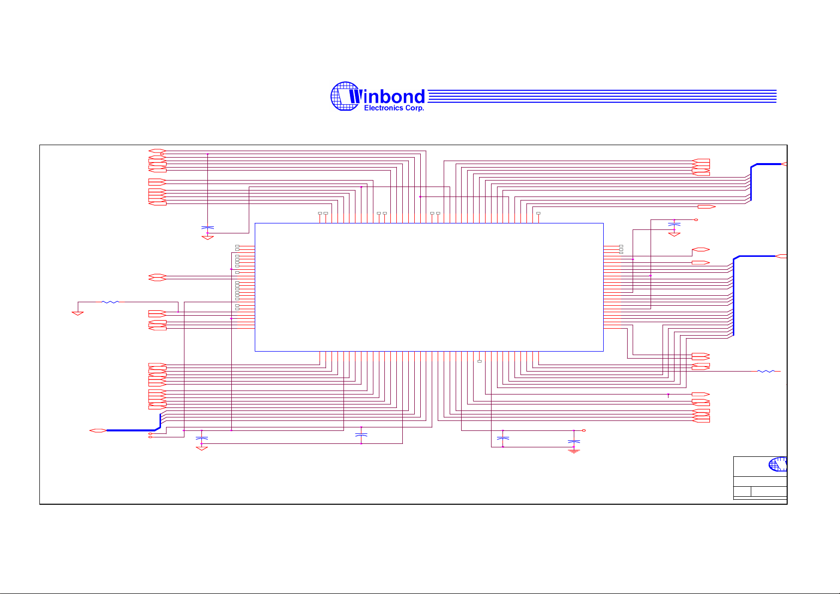
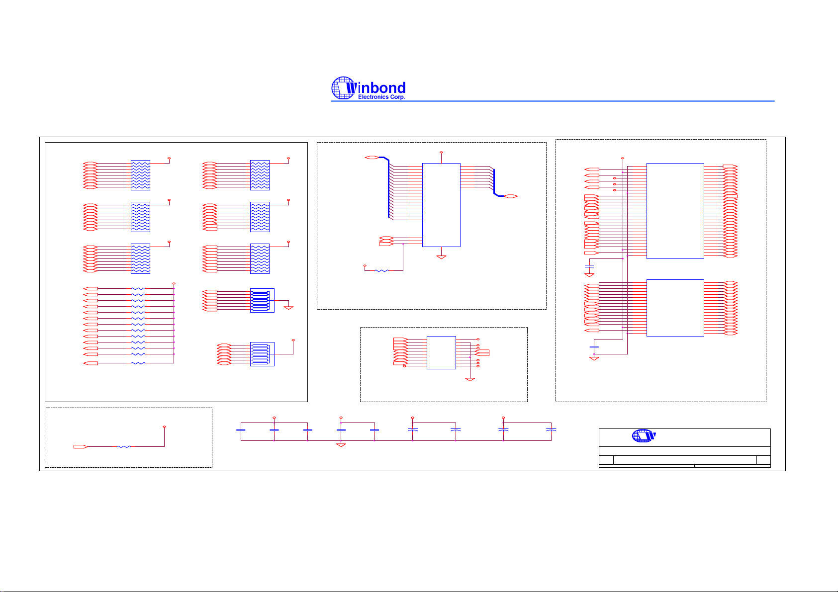
Recommended circuit for Desktop
W83626F FOR LPC TO ISA BRIDGE
Tuesday, November 16, 1999
Document Number
If do not use the GPIO function pin
please pull-down with a resistor.
IOW#
VCC5
IOR#
DACK3#
DRQ3
DACK1#
DRQ1
IRQ7
IRQ6
IRQ5
IRQ4
IRQ3
DACK2#
TC
MEMR#
NOTE9 :
For RTC functions power-on
setting used .
MEMW#
R3
1K
MASTER#
DRQ7
DACK7#
DRQ6
DACK6#
LPC TO ISA BRIDGE SET
W83626F/W83626D
PRELIMINARY
OWS#
DRQ2
IRQ9
RSTDRV
IOCHCK#
IOHCS#
100
101
102
C4
0.1UF
103
LA23
104
LA22
105
VCC5
106
LA21
107
LA20
108
LA19
109
LA18
110
GND
111
LA17
112
MEMR#
113
MEMW#
114
SD8
115
SD9
116
SD10
117
SD11
118
SD12
119
SD13
120
VCC5
121
SD14
122
SD15
123
MASTER#/RTCEN#
124
DRQ7
125
GND
126
DACK7#
127
DRQ6
128
DACK6#/HEFRAS
SBHE#
TC
BALE
DACK2#
GND
IRQ7
IRQ6
IRQ5
IRQ4
IRQ3
SYSCLK
DRQ1
REFRESH#
DACK1#
DRQ3
DACK3#
IOR#
W83626F
GND
SMEMR#
SMEMW#
OWS#
DRQ2
IRQ9
RSTDRV
IOW#
VCC5
IOCHCK#
SD3
SD4
SD5
SD6
SD7
6566676869707172737475767778798081828384858687888990919293949596979899
SD0
SD1
SD2
VCC5
GPIO7/IOHCS#
GPIO6/RTCCS#
GPIO5/IRQ8
GPIO4/PLED
GPIO3/IRQIN
IOCHRDY
GPIO2/MCCS#
GPIO1/KBCS#
U1
64
63
62
61
60
GND
59
AEN
58
SA19
57
SA18
56
SA17
55
VCC5
54
SA16
53
SA15
52
SA14
51
SA13
50
GND
49
SA12
48
SA11
47
SA10
46
SA9
45
VCC5
44
SA8
43
SA7
42
SA6
41
SA5
40
39
VCC5
C5
0.1UF
IOCHRDY
AEN
SD[7..0]
SA[19..0]
NOTE1:
LAD[3..0]
LAD[3..0]
IOCS16#
MEMCS16#
PCIRST#
DACK0#
DACK0#
LFRAM#
IRQ14
IRQ15
IRQ12
IRQ11
IRQ10
DRQ5
DACK5#
DRQ0
DACK0#
VCC5
IRQ14
IRQ15
IRQ12
IRQ11
IRQ10
IOCS16#
MEMCS16#
LFRAM#
PCIRST#
GND
LAD3
LAD2
LAD1
LAD0
VCC3
PCICLK
LDRQ#
SERIRQ
PWRDN#
AVCC3
14.318M
14MOUT1
14MOUT2
24.576M
AGND
SA0
SA1
SA2
SA3
SA4
80PCS#/KBEN#
ROMCS#
C6
10UF/16V
GPIO0/IRQ1
38
AVCC3
C2
0.1UF
DRQ5
DRQ0
VCC3
VCC5
C3
0.1UF
12345678910111213141516171819202122232425262728293031323334353637
C1
0.1UF
NOTE2:
If do not use the clock output function
,please connect to GND.(Pin 27,28&29)
MCCS#
KBCS#
IRQ1
ROMCS#
24.576M
OSC
14.318M
PWRDN#
SERIRQ
LDRQ#
PCICLK
FOR AC97 CODEC
Title
Size
B
Date:
R1
4.7K
626_1.SCH
Publication Release Date: Feb 2000
- 15 - Revision 0.50
Page 29
LPC TO ISA BRIDGE SET
W83626F/W83626D
PRELIMINARY
2
3
4
5
6
7
8
9
10
2
3
4
5
6
7
8
9
10
2
3
4
5
6
7
8
9
10
R3 4.7K
R4 1K
R5 1K
R6 1K
R13 1K
R11 8.2K
R10 8.2K
R1 1K
R2 1K
R9 1K
R8 1K
R7
R12
IOCHCK#
IOCHRDY
MASTER#
REFRESH#
MEMCS16#
IOCS16#
SMEMR#
SMEMW#
MEMW#
MEMR#
SA19
SA18
SA17
SA16
SA15
SA14
SA13
SA12
SA11
SA10
SA9
SA8
SA7
SA6
SA5
SA4
SA3
SA2
SA1
SA0
LA23
LA22
LA21
LA20
LA19
LA18
LA17
OWS#
IOR#
IOW#
PULL HIGH or PULL DOWN RESISTORPULL HIGH or PULL DOWN RESISTOR
PWRDN#
R15
1K
Resvered for wake-up
VCC5
RP2
1
8.2K
RP3
1
8.2K
RP4
1
8.2K
8.2K
8.2K
SD0
SD1
SD2
SD3
SD4
SD5
SD6
SD7
SD8
VCC5
SD9
SD10
SD11
SD12
SD13
SD14
SD15
IRQ14
IRQ15
VCC5
IRQ3
IRQ4
IRQ5
IRQ6
IRQ7
IRQ9
IRQ10
IRQ11
IRQ12
VCC5
DRQ0
DRQ1
DRQ2
DRQ3
DRQ5
DRQ6
DRQ7
LAD0
LAD1
LAD2
LAD3
LDRQ#
SERIRQ
LFRAM#
RP5
2
1
3
4
5
6
7
8
9
10
8.2K
VCC5
RP6
2
1
3
4
5
6
7
8
9
10
8.2K
VCC5
RP1
2
1
3
4
5
6
7
8
9
10
8.2K
RP8
2
3
4
5
6
7
8
2
3
4
5
6
7
8
1
8.2K
RP7
8.2K
VCC3
1
SA[18..0]
For 8M BIOS
ROM decode
MEMW#
MEMR#
ROMCS#
VCC5
NOTE4:
For ROMCS# power-on
seeting used
Flash ROM Decoder
PCIRST#
R14
4.7K
PCICLK
SERIRQ
LFRAM#
LDRQ#
LAD0
LAD1
LAD2
LAD3
VCC5
VCC5
32
U2
VCC
1
A18
30
A17
2
A16
3
A15
29
A14
28
A13
4
A12
25
A11
23
A10
26
A9
27
A8
5
A7
6
A6
7
A5
8
A4
9
A3
10
A2
11
A1
12
A0
31
WE#
24
OE#
22
CE#
LPC CON1
1
2
3
4
5
6
7
8
9
10
CON20B
13
DQ0
14
DQ1
15
DQ2
17
DQ3
18
DQ4
19
DQ5
20
DQ6
21
DQ7
GND
W29C040P-90
16
(PLCC)
11
12
13
14
15
16
17
18
19
20
5VSB
+12V
VCC3
-12V
-5V
+3.3V
SMDAT
SMCLK
SD[7..0]
RSTDRV
SMEMW#
SMEMR#
DACK3#
DACK1#
SYSCLK
DACK2#
IOCS16#
DACK0#
DACK5#
DACK6#
DACK7#
MASTER#
IRQ9
DRQ2
OWS#
IOW#
IOR#
DRQ3
DRQ1
IRQ7
IRQ6
IRQ5
IRQ4
IRQ3
TC
BALE
OSC
IRQ10
IRQ11
IRQ12
IRQ15
IRQ14
DRQ0
DRQ5
DRQ6
DRQ7
VCC5VCC5
-5V
-12V
+12V
CB5
0.1uF
CB6
0.1uF
J1
32
GND
33
RESDRV
34
+5V
35
IRQ9
36
-5V
37
DRQ2
38
-12V
39
0WS
40
+12V
41
GND
42
SMEMW#
43
SMEMR#
44
IOW#
45
IOR#
46
DACK3#
47
DRQ3
48
DACK1#
49
DRQ1
50
REF#
51
CLK
52
IRQ7
53
IRQ6
54
IRQ5
55
IRQ4
56
IRQ3
57
DACK2#
58
T/C
59
BALE
60
+5
61
OSC
62
GND
A/B CHANNEL
J2
19
MECS16#
20
IOCS16#
21
IRQ10
22
IRQ11
23
IRQ12
24
IRQ15
25
IRQ14
26
DACK0#
27
DRQ0
28
DACK5#
29
DRQ5
30
DACK6#
31
DRQ6
32
DACK7#
33
DRQ7
34
+5V
35
MASTER#
36
GND
C/D CHANNEL
IOCHCK#
MEMR#
MEMW#
1
2
SD7
3
SD6
4
SD5
5
SD4
6
SD3
7
SD2
8
SD1
9
SD0
10
IORDY
11
AEN
12
SA19
13
SA18
14
SA17
15
SA16
16
SA15
17
SA14
18
SA13
19
SA12
20
SA11
21
SA10
22
SA9
23
SA8
24
SA7
25
SA6
26
SA5
27
SA4
28
SA3
29
SA2
30
SA1
31
SA0
1
SBHE
2
LA23
3
LA22
4
LA21
5
LA20
6
LA19
7
LA18
8
LA17
9
10
11
SD08
12
SD09
13
SD10
14
SD11
15
SD12
16
SD13
17
SD14
18
SD15
IOCHCK#
SD7
SD6
SD5
SD4
SD3
SD2
SD1
SD0
IOCHRDY
AEN
SA19
SA18
SA17
SA16
SA15
SA14
SA13
SA12
SA11
SA10
SA9
SA8
SA7
SA6
SA5
SA4
SA3
SA2
SA1
SA0
SBHE#
LA23
LA22
LA21
LA20
LA19
LA18
LA17
MEMR#
MEMW#
SD8
SD9
SD10
SD11
SD12
SD13
SD14
SD15
LPC I/F ISA SLOT
VCC3
VCC5 VCC5
CB7
0.1uF
CB1
0.1uF
VCC3 VCC3
CB2
0.1uF
CB3
0.1uF
CB4
0.1uF
C7
10uF/16V
C8
10uF/16V
C9
10uF/16V
C10
10uF/16V
Title
W83626 FOR LPC TO ISA BRIDGE
Size Document Number Rev
626_2.SCH 0.3
B
Date: Sheet of
inbond
WINBOND ELECTRONICS CORP.
2 2Tuesday, August 17, 1999
Publication Release Date: Feb 2000
- 16 - Revision 0.50
Page 30

Recommended circuit for Notebook
LPC TO ISA BRIDGE SET
W83626F/W83626D
PRELIMINARY
Publication Release Date: Feb 2000
- 17 - Revision 0.50
Page 31
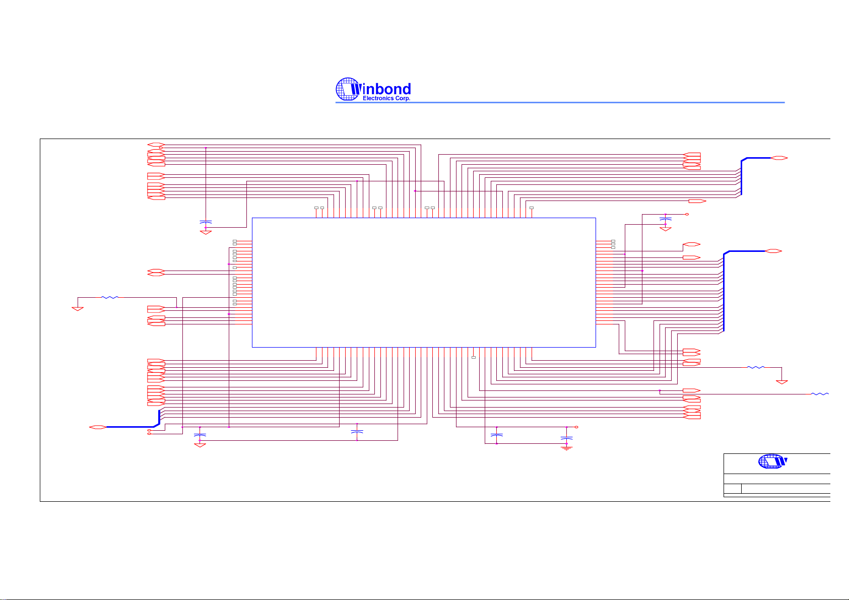
W83626F FOR LPC TO ISA BRIDGE
inbond
WINBOND ELECTRONICS CORP.
If do not use the GPIO function pin
please pull-down with a resistor.
For K/B functions power-on
For 25.000 MHz clock power-on
NOTE9 :
For RTC functions power-on
setting used .
LAD[3..0]
LAD[3..0]
LPC TO ISA BRIDGE SET
W83626F/W83626D
PRELIMINARY
IOW#
VCC5
IOR#
DACK3#
DRQ3
DACK1#
DRQ1
IRQ7
IRQ6
IRQ5
IRQ4
IRQ3
DACK2#
TC
100
101
102
C4
0.1UF
103
LA23
104
LA22
105
VCC5
106
LA21
107
LA20
108
LA19
109
LA18
110
GND
111
LA17
112
MEMR#
MEMW#
R3
1K
MASTER#
DRQ7
DACK7#
DRQ6
DACK6#
DRQ5
DACK0#
DRQ0
DACK0#
IRQ14
IRQ15
IRQ12
IRQ11
IRQ10
IOCS16#
MEMCS16#
LFRAM#
PCIRST#
VCC3
VCC5
C3
0.1UF
113
114
115
116
117
118
119
120
121
122
123
124
125
126
127
128
MEMR#
MEMW#
SD8
SD9
SD10
SD11
SD12
SD13
VCC5
SD14
SD15
MASTER#/RTCEN#
DRQ7
GND
DACK7#
DRQ6
DACK6#/HEFRAS
TC
GND
IRQ7
IRQ6
IRQ5
IRQ4
IRQ3
BALE
SBHE#
DACK2#
DRQ5
DACK5#
DRQ0
DACK0#
VCC5
12345678910111213141516171819202122232425262728293031323334353637
IRQ14
IRQ15
IRQ12
IRQ11
IRQ10
C1
0.1UF
SYSCLK
IOCS16#
DRQ1
REFRESH#
MEMCS16#
LFRAM#
DACK1#
PCIRST#
DRQ3
GND
DACK3#
LAD3
IOR#
LAD2
VCC5
W83626F
LAD1
GND
SMEMR#
VCC3
SMEMW#
PCICLK
OWS#
LDRQ#
SERIRQ
DRQ2
PWRDN#
IRQ9
AVCC3
RSTDRV
14.318M
IOW#
LAD0
SD3
SD4
SD5
SD6
SD7
IOCHCK#
14MOUT1
14MOUT2
24.576M
AGND
SA0
SA1
NOTE2:
If do not use the clock output function
,please connect to GND.(Pin 27,28&29)
6566676869707172737475767778798081828384858687888990919293949596979899
SD0
SD1
SD2
VCC5
GPIO7/IOHCS#
GPIO6/RTCCS#
GPIO5/IRQ8
GPIO4/PLED
GPIO3/IRQIN
IOCHRDY
GPIO2/MCCS#
GPIO1/KBCS#
SA2
SA3
SA4
80PCS#/KBEN#
ROMCS#
GPIO0/IRQ1
38
C6
10UF/16V
U1
64
63
62
61
60
GND
59
AEN
58
SA19
57
SA18
56
SA17
55
VCC5
54
SA16
53
SA15
52
SA14
51
SA13
50
GND
49
SA12
48
SA11
47
SA10
46
SA9
45
VCC5
44
SA8
43
SA7
42
SA6
41
SA5
40
39
AVCC3
C2
0.1UF
OWS#
DRQ2
IRQ9
RSTDRV
IOCHCK#
IOHCS#
VCC5
C5
0.1UF
IOCHRDY
AEN
MCCS#
KBCS#
IRQ1
ROMCS#
24.576M
OSC
14.318M
PWRDN#
SERIRQ
LDRQ#
PCICLK
SD[7..0]
SA[19..0]
NOTE1:
R1
4.7K
FOR AC97 CODEC
Title
Size Document Number
626_1.SCH
B
Tuesday, November 16, 1999
Date:
SD[7..0]
SA[19..0]
NOTE3:
setting used
NOTE8 :
setting used .
R2
4.7K
Publication Release Date: Feb 2000
- 18 - Revision 0.50
Page 32
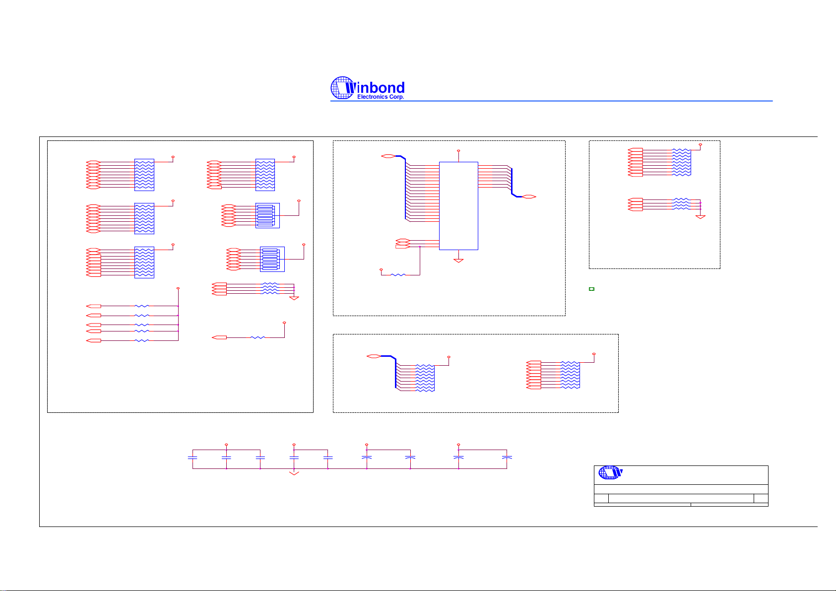
RP1
SA19 SD0
SA18
SA17
SA16
SA15
SA14
SA13
SA12
SA11
SA10
SA9
SA8
SA7
SA6
SA5
SA4
SA3
SA2
SA1
SA0
IRQ3
IRQ4
IRQ5
IRQ6
IRQ7
IRQ9
IRQ10
IOCHRDY
MEMW#
IOR#
MEMR#
IOW#
2
3
4
5
6
7
8
9
10
8.2K
RP2
2
3
4
5
6
7
8
9
10
8.2K
RP3
2
3
4
5
6
7
8
9
10
8.2K
R4 1K
R7 8.2K
R6 8.2K
R5 8.2K
R10
ISA I/F PULL HIGH
OR PULL DOWN RESISTORS
LPC TO ISA BRIDGE SET
W83626F/W83626D
PRELIMINARY
5VCC
VCC5
1
VCC5
1
VCC5
1
SD1
SD2
SD3
SD4
SD5
SD6
SD7
IRQ11
LAD0
LAD1
LAD2
LAD3
LDRQ#
SERIRQ
LFRAM#
LAD0
LAD1
LAD2
LAD3
LDRQ#
SERIRQ
LFRAM#
DRQ0
VCC5
DRQ1
DRQ2
DRQ3
RP4
2
3
4
5
6
7
8
9
10
8.2K
RP11
2
3
4
5
6
7
8
8.2K
2
3
4
5
6
7
8
1
3
5
7
VCC5
1
VCC3
1
RP10
8.2K
RP5
8.2K
VCC3
1
2
4
6
8
For 8M BIOS
ROM decode
SA[18..0]
MEMW#
ROMCS#
VCC5
MEMR#
R8
4.7K
VCC5
3216
1
A18
30
A17
2
A16
3
A15
29
A14
28
A13
4
A12
25
A11
23
A10
26
A9
27
A8
5
A7
6
A6
7
A5
8
A4
9
A3
10
A2
11
A1
12
A0
31
WE#
24
OE#
22
CE#
NOTE4:
R7 for ROMCS# power-on setting used.
The circuit is for flashable ROM
For BIOS read-only used can connect
OE# and CE# together to ROMCS# and
without MEMR# and MEMW#.
13
DQ0
14
DQ1
VCCGND
15
DQ2
17
DQ3
18
DQ4
19
DQ5
20
DQ6
21
DQ7
U2
W29C040P-90
(PLCC)
SD[7..0]
IRQ12
IRQ14
IRQ15
MEMCS16#
IOCS16#
IOCHK#
OWS#
SMEMW#
SMEMR#
DRQ5
DRQ6
DRQ7
MASTER#
NOTE6:
For disconnected signals used
No used signals
Flash ROM Decoder
VCC3
8.2K
PWRDN#
NOTE7 :
Reserved for wake_up function.
R9
4.7K
PD[0..7]
3
4
5
6
7
8
9
10
VCC5
RP6
12
4.7K
SLIN#
ERR#
BUSY
STB#
AFD#
INIT#
ACK#
PE
SLCT
3
4
5
6
7
8
9
10
VCC5
RP7
12
4.7K
PRT PULL-HI RESISTORS
RP9
12
3
4
5
6
7
8
9
10
8.2K
RP8
1
2
3
4
5
6
7
8
8.2K
VCC5 VCC5
CB5
0.1uF
CB1
0.1uF
VCC3 VCC3
CB2
0.1uF
CB3
0.1uF
CB4
0.1uF
C7
10uF/16V
C8
10uF/16V
C9
10uF/16V
C10
10uF/16V
inbond
WINBOND ELECTRONICS CORP.
Title
W83626F FOR LPC TO ISA BRIDGE
Size Document Number Rev
626_2.SCH 0.3
Custom
Date: Sheet of
2 4Tuesday, August 24, 1999
Publication Release Date: Feb 2000
- 19 - Revision 0.50
Page 33
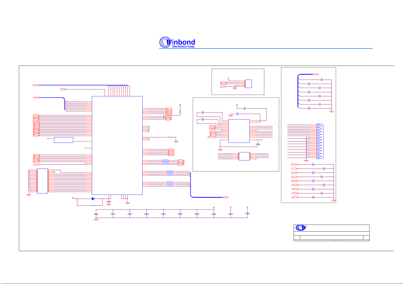
LPC TO ISA BRIDGE SET
W83626F/W83626D
PRELIMINARY
SA[0..10]
SD[0..7]
RSTDRV
AEN
IOCHRDY
IOR#
IOW#
TC
IRQ3
IRQ4
IRQ6
IRQ7
DRQ1
DACK1#
DRQ2
DACK2#
DRQ3
DACK3#
DRQ0 & DACK0# Set by
CR2B & CR2C
IRQ5
IRQ10
DRQ0
DACK0#
IRRX
IRTX
FIRRX
180PF C18
180PF C20
180PF C22
180PF
J2
1
14
2
15
3
16
4
17
5
18
6
19
7
20
8
21
9
22
10
23
11
24
12
25
13
DB25
C28
180PF C29
180PF C31
180PF
180PF C26
180PF
PD[0..7]
C16
180PFC17
180PFC19
180PFC21
180PFC23
180PFC30
180PFC32
C24
180PFC25
180PFC27
VCC5
FIRRX
C14
0.1UF/6.3V
C13
0.1UF/16V
SOUTA
RTSA
DTRA
DCDA
DSRA
CTSA
RIA
TC2
SINA
IRRX
IRTX
IR CONNECTOR
U5
12
C1+
14
C1-
15
C2+
16
C2-
7
T1IN
6
T2IN
20
T3IN
21
T4IN
8
R1OUT
5
R2OUT
26
R3OUT
22
R4OUT
19
R5OUT
10 11
GND VCC
MAX232E
NDCDA NSINA
NSOUTA NDTRA PE
GND NDSRA
NRTSA NCTSA SLCT
NRIA
PD[0..7]
VCC5
+
10UF/16V
+
TC3
SA[0..10]
IOHCS#
SD[0..7]
1
:NOTE5
J1
12
34
56
78
910
1112
1314
1516
1718
1920
2122
2324
2526
2728
2930
3132
3334
HEAD17X2
FDC
CS#
SD0
SD1
SD2 PD6
SD3
SD4
SD5 PD7
SD6
SD7
U4
NC
OUTPUT
24MHz OSC
IRRXH STB#
RWC# PD1 INIT#
INDEX# PD2
MOA# PD3
DSB# SLIN#
DSA#
MOB#
DIR# ERR#
STEP#
WD#
WE# ACK#
TRAK0#
WP#
RDATA# BUSY
HEAD#
DSKCHG#
VCC5
66
D0
67
D1
68
D2
69
D3
70
D4
71
D5
72
D6
73
D7
6
MR
62
AEN
5
IOCHRDY
63
IOR#
64
IOW#
97
T/C
44
IRQC/IRQ3
37
IRQD/IRQ4
99
IRQF/IRQ6
23
IRQE/IRQ7
39
DRQA/DRQ1
41
DACKA#/DACK1#
100
DRQB/DRQ2
98
DACKB#/DACK2#
4
DRQC/DRQ3
18
DACKC#/DACK3#
1N5817/19
7
CLKIN
8
SMI#
96
IRQA/GIO1
92
IRQB/GIO0
1
IRQG/PCICLK
91
IRQH/SERIRQ
94
IRRX2
95
IRTX2
93
IRQIN
3
IRRXH/SCI#
87
RWC#
81
INDEX#
79
MOA#
84
DSB#
83
DSA#
80
MOB#
89
DIR#
82
STEP#
86
WD#
85
WE#
78
TRAK0#
77
WP#
74
RDATA#
88
HEAD#
76
DSKCHG#
D1
R11
0
5
SA0
SA1
SA2
SA3
251525354555758596061
A0A1A2A3A4A5A6A7A8
CS#/A11
VCC
VCC
15
56
CB6
0.1UF
CB10
0.1UF
SA10
SA4
SA5
SA6
SA7
SA8
SA9
A10
CTSB#/A12
DSRB#/A13
DCDB#/A14
RIB#/A15
CB7
0.1UF
DSRA#
DCDA#
DTRB#
CTSA#
U3
34
33
32
31
RIA#
30
SINA
38
HEFRAS
35
36
47
48
49
50
42
SINB
PIRQMDS
43
46
45
29
ERR#
26
ACK#
24
BUSY
27
PE
28
SLCT
22
SLIN#
21
INIT#
20
AFD#
19
STB#
9
PD0
10
PD1
11
PD2
12
PD3
13
PD4
14
PD5
16
PD6
17
PD7
W83877F/AF/TF/ATF
RP13
1
3
5
7
33
1
3
5
7
1
3
5
7
CB8
0.1UF
VCC5
CTSA
DSRA
R13
DCDA
4.7K
RIA
SINA
SOUTA
DTRA
RTSA
R12
4.7K
ERR#
ACK#
BUSY
PE
SLCT
2
SLIN#
4
INIT#
6
AFD#
8
STB#
RP12
2
4
6
8
33
RP14
2
4
6
8
33
+
CB9
0.1UF
PD0
PD4
PD5
PD6
PD7
10UF/16V
COM
PD[0..7]
+
TC1
10UF/16V
75
A9
SOUTA/PENFDC
DTRA#/HEFRAS
RTSA#/PPNPCVS
SOUTB/PIRQMDS
RTSB#/PGOIQSEL
VSS
VSS
VSS
VSS
254065
90
CB11
0.1UF
VCC5
COMA (UARTA)
TC4
10UF/16V
C15
0.1UF/16V
J3
1
3
5
7
9
CN2X5B
J4
1
2
3
4
5
HEADER 5
C12
0.1UF/6.3V
13
V+
17
V-
NSOUTA
2
T1OUT
NRTSA
3
T2OUT
NDTRA
1
T3OUT
28
T4OUT
NDCDA
9
R1IN
NSINA
4
R2IN
NDSRA
27
R3IN
NCTSA
16
R4IN
NRIA
18
R5IN
(SOP)
2
4
6
8
10
VCC5
C11
0.1UF/16V
STB#
AFD#
INIT#
SLIN#
ERR#
ACK#
BUSY
SLCT
PRT
-12V+12V
+
TC5
10UF/16V
PD0
PD1
PD2
PD3
PD4
PD5
STB#
AFD#
PD0
ERR#
PD1
INIT#
PD2
SLIN#
PD3
PD4
PD5
PD6
PD7
ACK#
BUSY
AFD#
PE
PE
SLCT
inbond
Title
WINBOND ELECTRONICS CORP.
W83626F FOR LPC TO ISA BRIDGE
Size Document Number Rev
626_3.SCH
Custom
Date: Sheet of
3 4Tuesday, August 24, 1999
0.3
Publication Release Date: Feb 2000
- 20 - Revision 0.50
Page 34

LPC TO ISA BRIDGE SET
W83626F/W83626D
PRELIMINARY
Publication Release Date: Feb 2000
- 21 - Revision 0.50
 Loading...