

Page 1

W83601R/602R
Winbond SMBus GPI/O
Page 2
W83601R/602R
PRELIMINARY
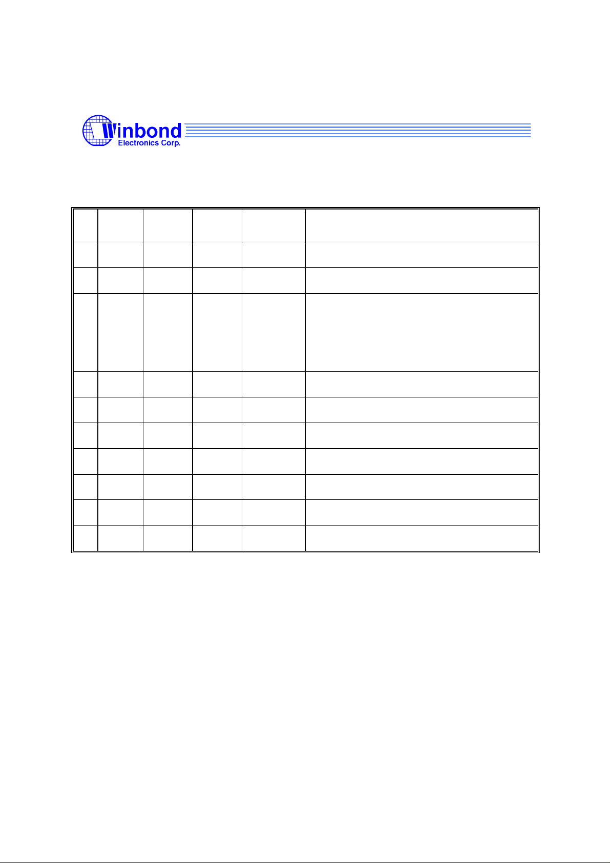
W83601R/602R Data Sheet Revision History
Pages Dates Version Version
on Web
1
2
3
4
5
6
7
8
9
n.a. n.a. All the version before 0.30 are for internal use.
n.a. 99/8 0.3 n.a. First publication.
P.4,5
P.6
P.10
P.13
P.10 99/9 0.32 n.a. CR15 bit 3 description.
99/8 0.31 n.a. Change Pin Description of W83601R pin 3,4,5.
Main Contents
Change Pin Description of W83602R pin 3,4.
Update Register Table.
CR16 is a reserved register. Please ignore it.
Change INT output description.
10
Please note that all data and specifications are subject to change without notice. All the
trade marks of products and companies mentioned in this data sheet belong to their
respective owners.
LIFE SUPPORT APPLICATIONS
These products are not designed for use in life support appliances, devices, or
systems where malfunction of these products can reasonably be expected to result in
personal injury. Winbond customers using or selling these products for use in such
applications do so at their own risk and agree to fully indemnify Winbond for any
damages resulting from such improper use or sales.
Publication Release Date: Aug. 1999
- 1 - Revision 0.32
Page 3

W83601R/602R
Preliminary
1. GENERAL DESCRIPTION
The W83601R/602R are general purpose input/output ICs with SMBusTM. W83601R provides 15
GPI/O pins. W83602R provides 9 GPI/O pins and ACPI power control function for STR.
W83601R/602R both provides SMBusTM address setting pins to set the address during power- on
reset or from external reset.
W83601R SMBusTM Address is :
W83602R SMBusTM Address is :
W83601R/602R also provides a interrupt to inform system that a transition occurs on General
Purpose(GP) input pins.
0 0 1 1 A2 A1 A0 R/W
0 0 1 1 0 A1 A0 R/W
2. FEATURES
• SMBus compliance with 3.3V voltage levels
• Two ports GPI/O which provides more flexibility
• Issue interrupt to notify system that a event occurs
• GP output can be level or pulse mode
• Interrupt output can be level or pulse mode
• Internal power-on reset or external RST# pin reset
• Programmable POWER LED output
• ACPI power management for Suspend To Ram (STR) (only for W83602R)
3. PACKAGE
• 20-pin SSOP
Publication Release Date: Aug. 1999
- 2 - Revision 0.32
Page 4
4. KEY SPECIFICATIONS
• Supply Voltage 5V
• Operating Supply Current 1 mA typ.
• Operating Temperature 0 - 70 °C
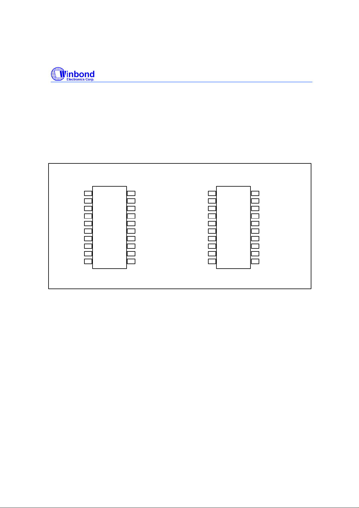
5. PIN CONFIGURATION FOR W83601R/602R
W83601R/602R
Preliminary
SCLK
SDAT
GP20/A0
GP21/A1
GP22/A2
GP10
GP11
GP23
GP24
VSS
W83601R
1
2
3
4
5
6
7
8
9
10
20
19
18
17
16
15
14
13
12
11
20SSOP 20SSOP
VDD
RST#
GP17/INT
GP16
GP15
GP14
GP13
GP12
GP26/INT
GP25
SCLK
SDAT
GP20/A0
GP21/A1
CTL3VSB
GP10
GP11
CTLSTRV
S5IN#
VSS
W83602R
1
2
3
4
5
6
7
8
9
10
20
19
18
17
16
15
14
13
12
11
VDD
RST#
GP17/INT
GP16
GP15
GP14
GP13
GP12
PWCTLIN#
PS_ON#
Publication Release Date: Aug. 1999
- 3 - Revision 0.32
Page 5
W83601R/602R
Preliminary
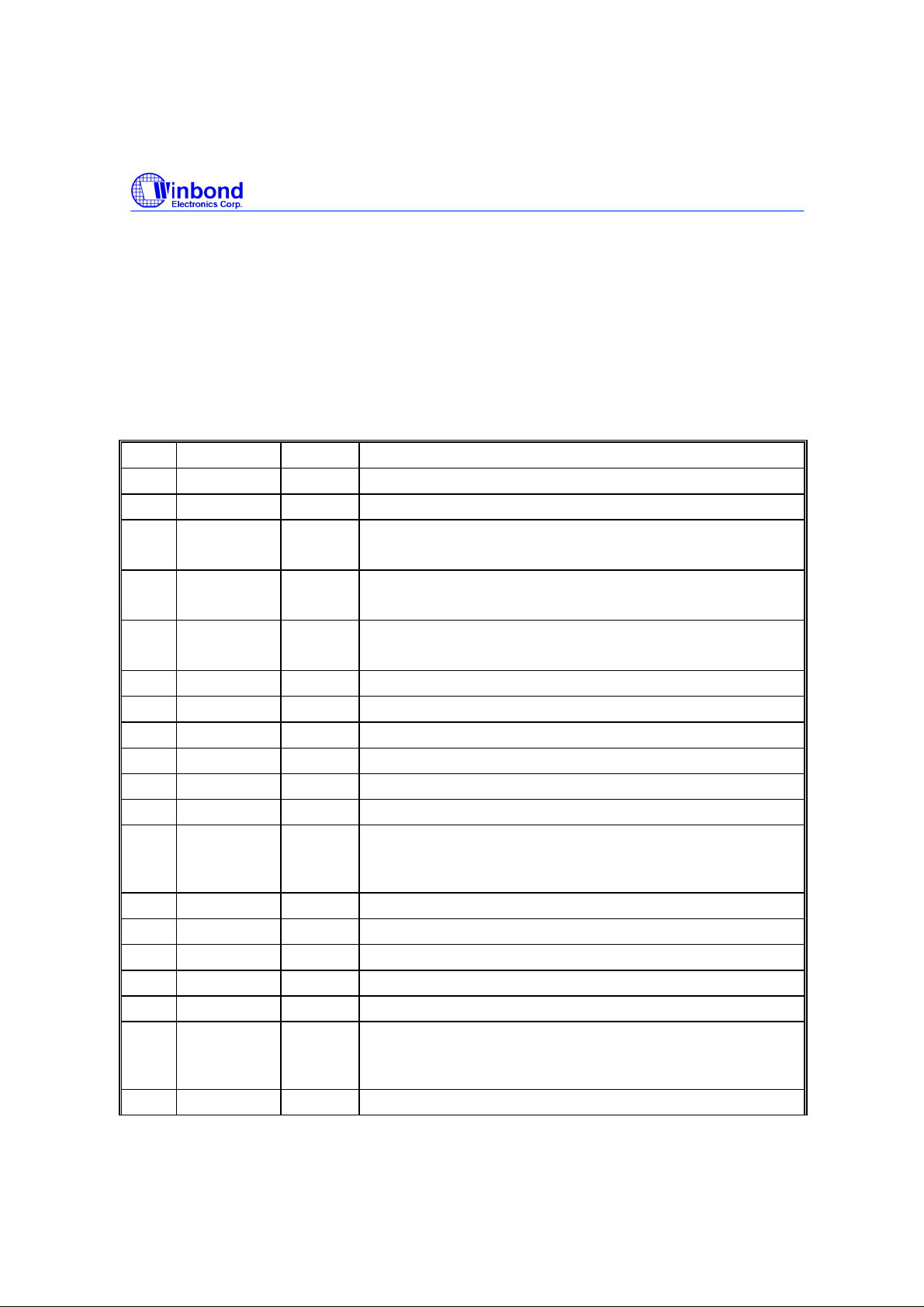
6. PIN DESCRIPTION
Note: Please refer to Section 13.2 DC CHARACTERISTICS for details.
I/OD
- TTL level bi-directional pin open drain output with 12 mA sink capability
24t
I/O
- TTL level bi-directional pin with 24 mA source-sink capability
24t
INt - TTL level input pin
INtd - TTL level input pin with internal pull down resistor
INts - TTL level Schmitt-trigger input pin
W83601R UNIVERSAL GENERAL PURPOSE I/O PORT FOR I2C BUS
PIN SYMBOL I/O FUNCTION
1 SCL INts SMBus Clock. (I2C clock)
2 SDA I/OD12 SMBus bi-directional Data.(I2C data)
3 GP20
A0
4 GP21
A1
5 GP22
A2
6 GP10 I/OD24 General Purpose I/O default input.
7 GP11 I/OD24 General Purpose I/O default input.
8 GP23 I/OD24 General Purpose I/O default input.
9 GP24 I/OD24 General Purpose I/O default input.
10 VSS PWR Ground Pin.
11 GP25 I/OD24 General Purpose I/O default input.
12 GP26
INT
13 GP12 I/OD24 General Purpose I/O default input.
14 GP13 I/OD24 General Purpose I/O default input.
15 GP14 I/OD24 General Purpose I/O default input.
16 GP15 I/OD24 General Purpose I/O default input.
17 GP16 I/OD24 General Purpose I/O default input.
18 GP17
INT
19 RST# INts Reset signal input.
I/O
24
INtd
I/O
24
INtd
I/O
24
INtd
I/OD
OD24
I/OD
OD24
General Purpose I/O . This pin is a setting pin for SMBus(I2C)
address bit 0 during power-on reset or RST# pin reset.
General Purpose I/O . This pin is a setting pin for SMBus(I2C)
address bit 1 during power-on reset or RST# pin reset.
General Purpose I/O . This pin is a setting pin for SMBus(I2C)
address bit 2 during power-on reset or RST# pin reset.
General Purpose I/O default input.
24
Auto-generate Interrupt signal when detetecting a transition on
GPI inputs. This interrupt is either on pin12 or pin18.
General Purpose I/O default input.
24
Auto-generate Interrupt signal when detetecting a transition on
GPI inputs. This interrupt is either on pin12 or pin18
Publication Release Date: Aug. 1999
- 4 - Revision 0.32
Page 6
W83601R/602R
Preliminary
20 VDD PWR Power Pin.
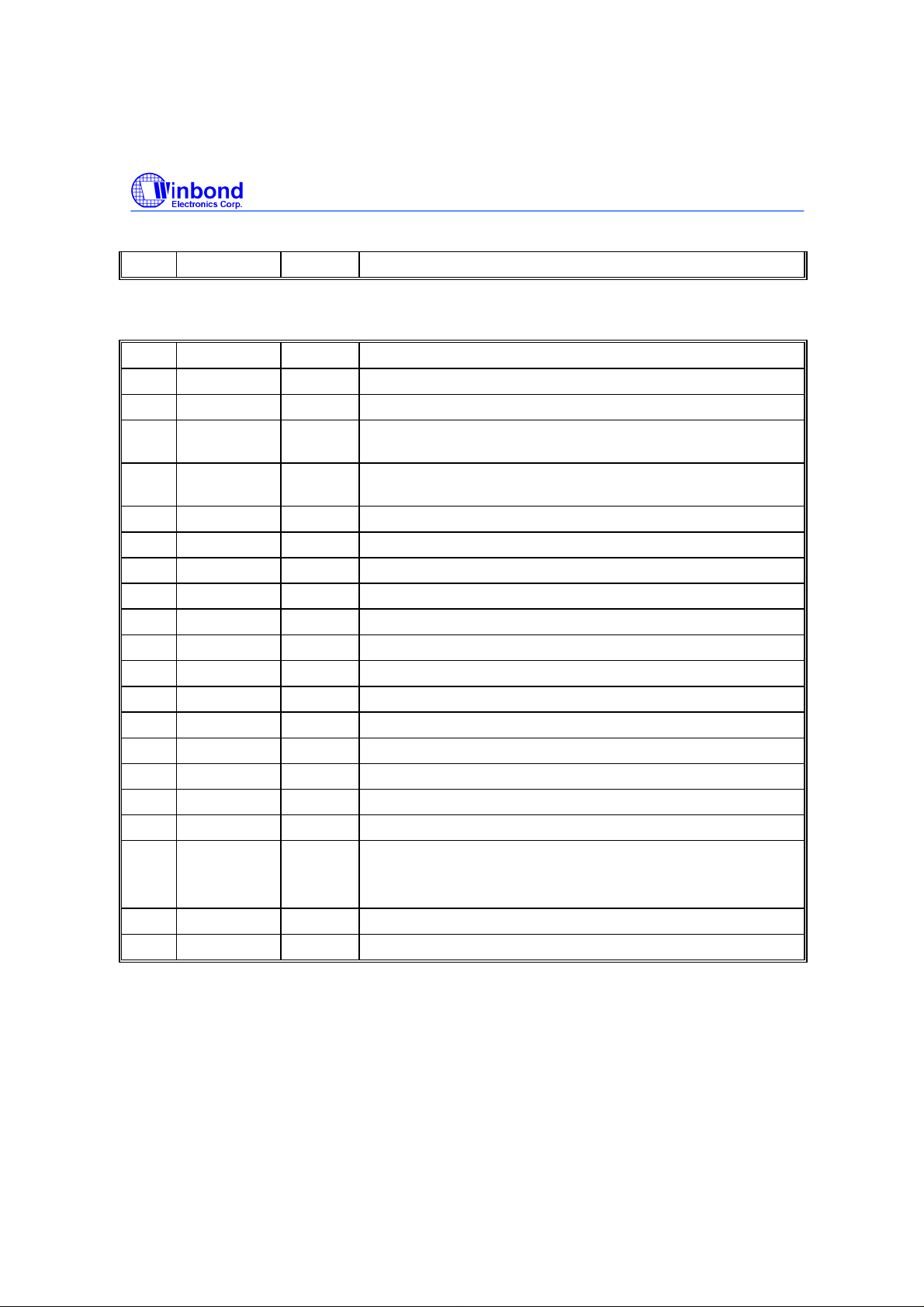
W83602R UNIVERSAL GENERAL PURPOSE I/O PORT FOR I2C BUS & ACPI
POWER CONTROL
PIN SYMBOL I/O FUNCTION
1 SCL INts SMBus Clock. (I2C clock)
2 SDA I/OD12 SMBus bi-directional Data.(I2C data)
3 GP20/A0 I/O24 General Purpose I/O. Power on setting for SMBus(I2C) address
bit 0.
4 GP21/A1 I/O24 General Purpose I/O. Power on setting for SMBus(I2C) address
bit 1.
5 CTL3VSB OD24 Control 3VSB and 3VCC power source for ACPI features.
6 GP10 I/OD24 General Purpose I/O default input.
7 GP11 I/OD24 General Purpose I/O default input.
8 CTLSTR OD24 Suspend to RAM power control output.
9 S5IN# INt S5# signal input.
10 VSS PWR Ground Pin.
11 PS_ON# OD24 ATX power power on_off control.
12 PWCTLIN# INt Connected to W83627F/HF power control output .
13 GP12 I/OD24 General Purpose I/O default input.
14 GP13 I/OD24 General Purpose I/O default input.
15 GP14 I/OD24 General Purpose I/O default input.
16 GP15 I/OD24 General Purpose I/O default input.
17 GP16 I/OD24 General Purpose I/O default input.
18 GP17
INT
19 RST# INts Reset signal input.
20 VDD PWR Power Pin.
I/OD
OD24
General Purpose I/O default input.
24
Auto-generate Interrupt signal when detetecting a transition on
GPI inputs.
Publication Release Date: Aug. 1999
- 5 - Revision 0.32
Page 7
W83601R/602R
7. REGISTERS
7.1 BRIEF OF REGISTER CONTENTS
INDEX R/W DEFAULT REGISTERS DESCRIPTION
00h R - GP Port 1: Input Port Data Register
01h R/W 00 GP Port 1: Output Port Data Register
02h R/W f0 GP Port 1: Polarity Inversion Register
03h R/W ff GP Port 1: Input/Output Configuration Register
04h R/W 00 GP Port 1: Output style control Register.
05h R - GP Port 1: Input Latched Data Register.
06-07h - - Reserved Register
08h R - GP Port 2: Input Port Register
09h R/W 00 GP Port 2: Output Port Register
0Ah R/W 70 GP Port 2: Polarity Inversion Register
0Bh R/W 7f GP Port 2: Input/Output Configuration Register
0Ch R/W 00 GP Port 2: Output style control Register.
0Dh R - GP Port 2: Input Latched Data Register.
0E-0Fh - - Reserved Register
10h R 00 GP Port 1: Interrupt Status Register.
11h R 00 GP Port 2: Interrupt Status Register
12h R/W 00 GP Port 1: Interrupt Enable Register
13h R/W 00 GP Port 2: Interrupt Enable Register
14h R/W 00 Mode Configuration Register
15h R/W 00 Power LED Configuration Register
16-1Fh - - Reserved Register
20h R 60 Chip ID High Byte Register
21h R 12
22
Chip ID Low Byte Register (W83601R)
Chip ID Low Byte Register (W83602R)
Preliminary
Publication Release Date: Aug. 1999
- 6 - Revision 0.32
Page 8

W83601R/602R
Preliminary
7.2 W83601R/602R REGISTERS DESCRIPTIONS
CR00 (GP Port 1: Input port Data Register, Default 0x-- , Read Only)
This register is a data port for input only. It reflects the incoming logic levels of the pins whether the pins
is defined as an input mode by CR03. It will be inverted data by CR02.
Bit 7 ~ 0: GP17 ~ GP10 Input Data Port.
CR01 (GP Port 1: Output port Data Register, Default 0x00, Read/Write)
This register is a data port for output only. It reflects the outgoing logic levels of the pins whether the pins
is defined as an output mode by CR03. This register will reflect the value of output Flip-flop while read
access. The output data will be inverted or changed output style by CR02 or CR04.
Bit 7 ~ 0: GP17 ~ GP10 Output Data Port.
CR02 (GP Port 1: Polarity Inversion Register, Default 0xf0, Read/Write)
This register enables polarity inversion of pins defined as input or output by CR03.
When set to a "1", the incoming/outgoing port value is inverted.
When set to a "0", the incoming/outgoing port value is the same as in data register.
Bit 7 ~ 0: GP17 ~ GP10 Polarity Iversion Register.
CR03 (GP Port 1: Input/Output Configuration Register, Default 0xff, Read/Write)
This register selects Input or Output mode of pins.
When set to a "1", respective GPIO port is programmed as an input port.
When set to a "0", respective GPIO port is programmed as an output port.
Bit 7 ~ 0: GP17 ~ GP10 Input/Output Configuration Register.
CR04 (GP Port 1: Output Style Control Register, Default 0x00, Read/Write)
This register selects Output style of pins as level or pulse.
When set to a "1", respective GPIO port is programmed as an pulse signal.
When set to a "0", respective GPIO port is programmed as an level signal.
Bit 7 ~ 0: GP17 ~ GP10 Output Style Control Register.
CR05 (GP Port 1: Input latched data Register, Default 0x--, Read Only)
This register will latch Port 1 data while power on or RST# pin low, which is controlled by CR14h bit 0 .
Bit 7 ~ 0: GP17 ~ GP10 Input latched data .
CR06-07 Reserved Register
Publication Release Date: Aug. 1999
- 7 - Revision 0.32
Page 9

W83601R/602R
Preliminary
CR08 (GP Port 2: Input port Data Register, Default 0x--, Read Only )
This register is a data port for input only. It reflects the incoming logic levels of the pins whether the pins
is defined as an input mode by CR0B. It will be inverted data by CR0A.
Bit 7: Reserved.
Bit 6 ~ 0: GP26 ~ GP20 Input Data Port.
CR09 (GP Port 2: Output port Data Register, Default 0x00, Read/Write)
This register is a data port for output only. It reflects the outgoing logic levels of the pins whether the pins
is defined as an output mode by CR0B. This register will reflect the value of output Flip-flop while read
access. The output data will be inverted or changed output style by CR0A or CR0C.
Bit 7: Reserved.
Bit 7 ~ 0: GP26 ~ GP20 Output Data Port.
CR0A (GP Port 2: Polarity Inversion Register, Default 0x70, Read/Write)
This register enables polarity inversion of pins defined as input or output by CR0B.
When set to a "1", the incoming/outgoing port value is inverted.
When set to a "0", the incoming/outgoing port value is the same as in data register.
Bit 7: Reserved.
Bit 6 ~ 0: GP26 ~ GP20 Polarity Inversion Register.
CR0B (GP Port 2: Input/Output Configuration Register, Default 0x7f, Read/Write)
This register selects Input or Output mode of pins.
When set to a "1", respective GPIO port is programmed as an input port.
When set to a "0", respective GPIO port is programmed as an output port.
Bit 7: Reserved.
Bit 6 ~ 0: GP26 ~ GP20 Input/Output Configuration Register.
CR0C (GP Port 2: Output Style Control Register, Default 0x00, Read/Write)
This register selects Output style of pins as level or pulse.
When set to a "1", respective GPIO port is programmed as an pulse signal.
When set to a "0", respective GPIO port is programmed as an level signal.
Bit 7: Reserved.
Bit 6 ~ 0: GP26 ~ GP20 Output Style Control Register.
CR0D (GP Port 2: Input latched data Register, Default 0x--, Read Only)
This register will latch Port 2 data while power on or RST# pin low, which is controlled by CR14h bit 1 .
Bit 7: Reserved.
Bit 6 ~ 0: GP26 ~ GP20 Input latched data, which bit 2-0 are SMBus address bit A2-A0 .
CR0E-0F Reserved Register
Publication Release Date: Aug. 1999
- 8 - Revision 0.32
Page 10

W83601R/602R
Preliminary
CR10 (GP Port1: Interrupt Status Register , Default 0x00, Read Only)
Bit 7-0 : = 1, a transition occurs at pin GP17-GP10.
If GP17/INT is selected as interrupt function, bit 7 of this register will always be 0.
A read to this register will clear this register.
CR11 (GP Port2: Interrupt Status Register , Default 0x00, Read Only)
Bit 7 : = Reserved.
Bit 6-0 : = 1, a transition occurs at pin GP26-GP20.
If GP26/INT is selected as interrupt function, bit 6 of this register will always be 0.
A read to this register will clear this register.
CR12 (GP Port 1: Interrupt Enable Register , Default 0x00 , Read/Write)
Bit 7-0 : = 0, disable GP17-GP10 interrupt output when interrupt function is selected.
CR13 (GP Port 2: Interrupt Enable Register , Default 0x00 , Read/Write)
Bit 7-6 : = Reserved.
Bit 5-0 : = 0, disable GP26-GP20 interrupt output when interrupt function is selected.
CR14 Mode Configuration Register (Default 0x00, Read/Write)
Bit 7 : = 1, Set GP/INT pin as INT function. 0, set GP/INT pin as GP function.
Bit 6 : = 1, Set INT function at GP26(pin 12). 0 , Set INT function at GP17(pin 18).
W83602R INT function is only at GP17.
Bit 5 : = 1, Set INT output pin as pulse mode. 0, set INT output pin as level mode.
Bit 4 : = 1, Set INT output pin polarity is 1 (normal high) . 0, set INT output pin polarity is 0 (normal low).
This bit is only for W83601R.
Bit 3 : = 1, Port 2 (CR09h-CR0Ch,CR11h,CR13h) registers can be reset to default data by RST# pin. 0
,Port 2 (CR09h-CR0Ch) can not be reset by RST# pin.
Bit 2 : = 1, Port 1 (CR01h-CR04h,CR10h,CR12h) registers can be reset to default data by RST# pin. 0
,Port 1 (CR01h-CR04h) can not be reset by RST# pin.
Bit 1 : = 1, Port 2 CR0Dh can be latched not only by RST# pin but also power-on period. 0, Port 2
CR0Dh can only be latched by power-on period.
Bit 0 : = 1, Port 1 CR05h can be latched not only by RST# pin but also power-on period. 0, Port 1
CR05h can only be latched by power-on period.
Publication Release Date: Aug. 1999
- 9 - Revision 0.32
Page 11

W83601R/602R
Preliminary
CR15 Power LED Configuration Register (Default 0x00, Read/Write)
Priority of LED function is highest.
Bit 7 : = 1, Enable LED function . 0, Disable LED funciton.
When LED function is enable, GP function is ignored despite of input or output.
Bit 6-4 : LED frequency selection.
= 111, LED pin is tri-state(OD pin) or drived high(O pin).
= 110, LED pin is a 1 Hz toggle pulse with 50 duty cycle.
= 101, LED pin is a 1/2 Hz toggle pulse with 50 duty cycle.
= 100, LED pin is a 1/4 Hz toggle pulse with 50 duty cycle.
= 000, LED pin is drived low.
Bit 3 : = GP port selection.
0, Select GP port 1 as LED function if bit 7 is set to 1.
1, Select GP port 2 as LED function if bit 7 Is set to 1.
As W83602R, setting this bit 1 is meaningless.
Bit 2-0 : GP pin selection.
=110-000, GP16-GP10 can be selected as LED output when bit 3 is 0.
=101-011, GP25-GP23 can be selected as LED output when bit 3 is 1.
As W83602R, only GP16-GP10 can be selected as LED output.
CR16-1F Reserved Register
CR20 (Chip ID High Byte, Read Only)
Bit 7-0 : = 0x60.
CR21 (Chip ID Low Byte, Read Only)
Bit 7-0 : = 0x12 (for W83601R).
= 0x22 (for W83602R).
NOTE: W83602R has no GP22-GP26. All the corresponding register has no effect on W83602R.
Publication Release Date: Aug. 1999
- 10 - Revision 0.32
Page 12
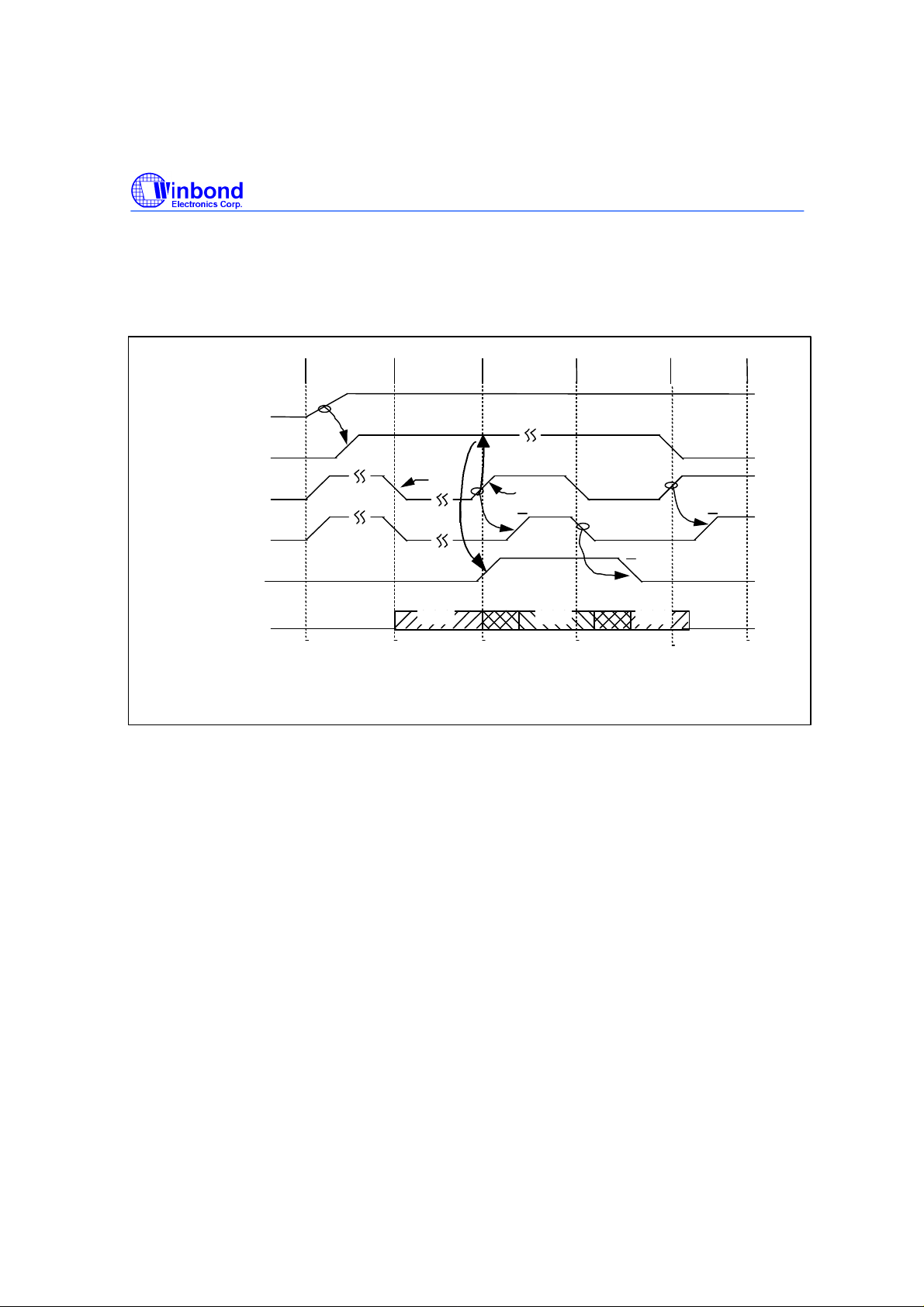
8. FUNCTION DESCRIPTIONS
POWER
*
FIRST AC ON
~ S5 STATE ~
POWER ON
~ S0 STATE ~
STR *
SOFT OFF
~ S5 STATE ~
3VCC
3VSB 3VCC
*NOTE 1: IT CAN WAKE UP POWER FROM POWER BUTTON, KEYBOARD/MOUSE,
SPECIAL DEFINED
~ S0 STATE ~
8.1 CTLSTRV TIMING WAVEFORMS (ONLY FOR W83602R)
W83601R/602R
Preliminary
5VSB
S5IN#
NOTE1
PS_ON#
CTLSTRV
DRAM_VOLTAG
*NOTE 2: IT CAN SUSPEND TO RAM BY OS OR
SUSPEND
T1= 5+1MS
RESUME
from S3
NOTE2
T2=500+125MS
- 11 - Revision 0.32
Publication Release Date: Aug. 1999
Page 13
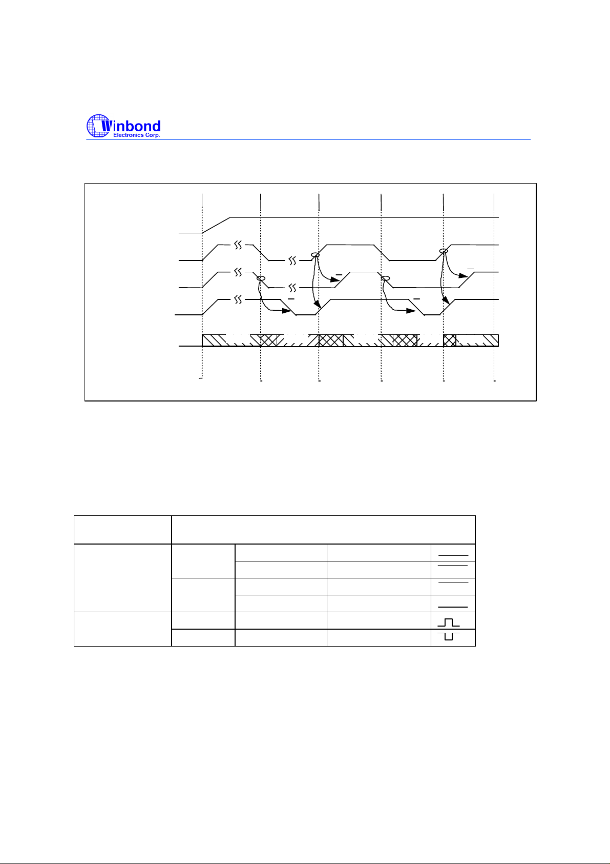
8.2 CTL3VSB Timing Waveforms(Only for W83602R)
First AC On
~ S5 state ~
Power On
~ S0 state ~
T2=500+125MS
Soft OFF
~ S5 state ~
3VCC
3VSB
3VCC
T2=500+125MS
3VSB
3VSB
W83601R/602R
Preliminary
8.3 GPI/O Output Mode :
5VSB
PWRCTL#
PS_ON#
CTL3VSB
3VSB_Voltage
Suspend to RAM Resume from S3
~ S3 STATE ~
t1= 5+1ms
~ S0 state ~
t1= 5+1ms
8.3.1 GPO output
Tow output modes for GPO. One is LEVEL and the other is PULSE.
GPO Output Style Polarity Output Port
Register
0 0 0
1 1
Level 1 0 1
1 0
Pulse 0 write 1 Active
1 write 1 Active
- 12 - Revision 0.32
Output Value at Pin Wave
Publication Release Date: Aug. 1999
Page 14
W83601R/602R
Preliminary
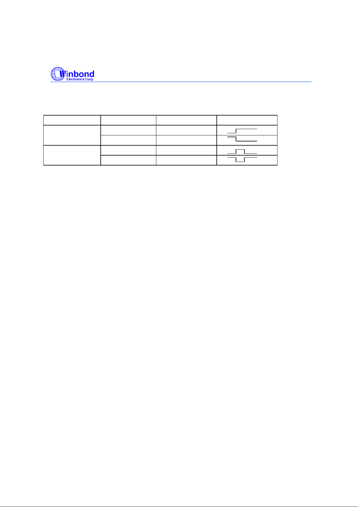
8.3.2 INT output
Two output modes for INT pin. One is LEVEL mode and the other is PULSE.
INT Output Mode Polarity Output Wave
Level 0(normal low) 1
1(normal high) 0
Pulse 0(normal low) High Pulse
1(normal high) Low Pulse
In Level mode, if INT is activated, it will be de-activated when interrupt status registers are read.
In Pulse mode, interrupt will be activated again unless all enabled interrupt status registers are read.
8.3.3 GPI interrupt status
Once a transition occurs at GPI input pins, interrupt status registers(CR10, CR11) will be set. At
the mean time, if interrupt function is enable, INT pin will generate a interrupt. Reading these interrupt
registers will clear themselves and reset interrupt. If an interrupt occurs but no read to interrupt status
registers, interrupt will not be generated again.
Publication Release Date: Aug. 1999
- 13 - Revision 0.32
Page 15
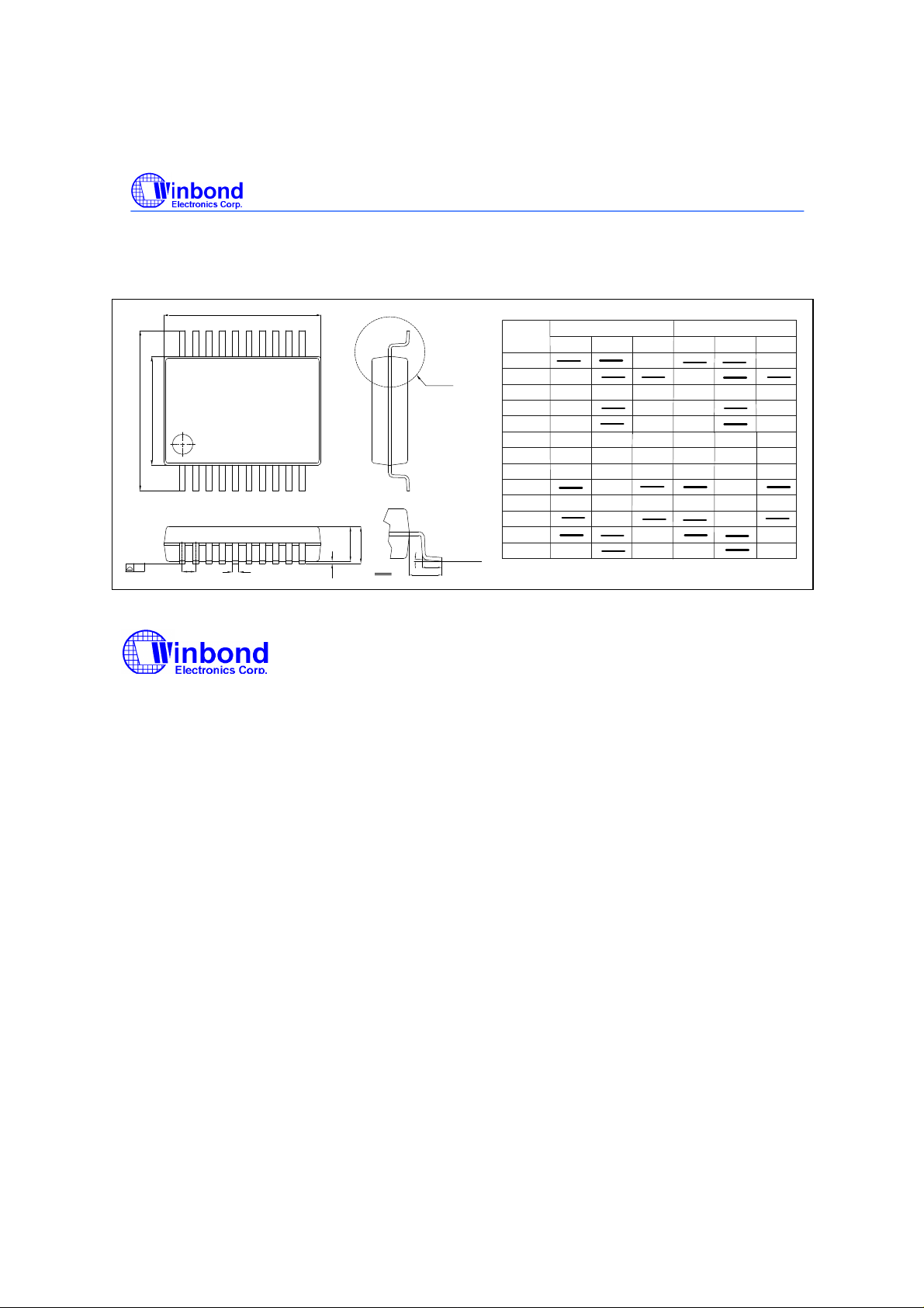
9. PACKAGE DRAWING AND DIMENSIONS
2
20 SSOP-209 mil
D
11
H
E
E
SEATING PLANE
Y
1
e
b
10
A2 A
A1
DETAIL A
θ
DTEAIL A
L
L1
SEATING PLANE
SYMBOL
A
A1
A2
b
c
D
E
H
E
e
L
L1
Y
θ
Preliminary
DIMENSION IN MM
MIN. NOM MAX. MAX.NOM
0.05
1.751.65
0.22 0.38
0.09 0.25
6.90
7.20
5.00
5.30
7.80
7.40
0.65
0.55 0.75
1.25
0
DIMENSION IN INCH
MIN.
2.00
0.002
0.065
1.85
7.50
5.60
8.20
0.95 0.037
0.10
8
0.069
0.009 0.015
0.004 0.010
0.272 0.2950.283
0.197
0.209
0.291
0.0256
0.021 0.030
0.050
0
0.079
0.073
0.220
0.3230.307
0.004
8
Headquarters
No. 4, Creation Rd. III
Science-Based Industrial Park
Hsinchu, Taiwan
TEL: 886-35-770066
FAX: 886-35-789467
www: http://www.winbond.com.tw/
Winbond Electronics (H.K.) Ltd.
Rm. 803, World Trade Square, Tower II
123 Hoi Bun Rd., Kwun Tong
Kowloon, Hong Kong
TEL: 852-27516023-7
FAX: 852-27552064
Winbond Electronics
(North America) Corp.
2730 Orchard Parkway
San Jose, CA 95134 U.S.A.
TEL: 1-408-9436666
FAX: 1-408-9436668
Taipei Office
11F, No. 115, Sec. 3, Min-Sheng East Rd.
Taipei, Taiwan
TEL: 886-2-7190505
FAX: 886-2-7197502
TLX: 16485 WINTPE
Please note that all data and specifications are subject to change without notice. All the
trade marks of products and companies mentioned in this data sheet belong to their
respective owners.
These products are not designed for use in life support appliances, devices, or systems
where malfunction of these products can reasonably be expected to result in personal
injury. Winbond customers using or selling these products for use in such applications
do so at their own risk and agree to fully indemnify Winbond for any damages resulting
from such improper use or sale.
Publication Release Date: Aug. 1999
- 14 - Revision 0.32
Page 16
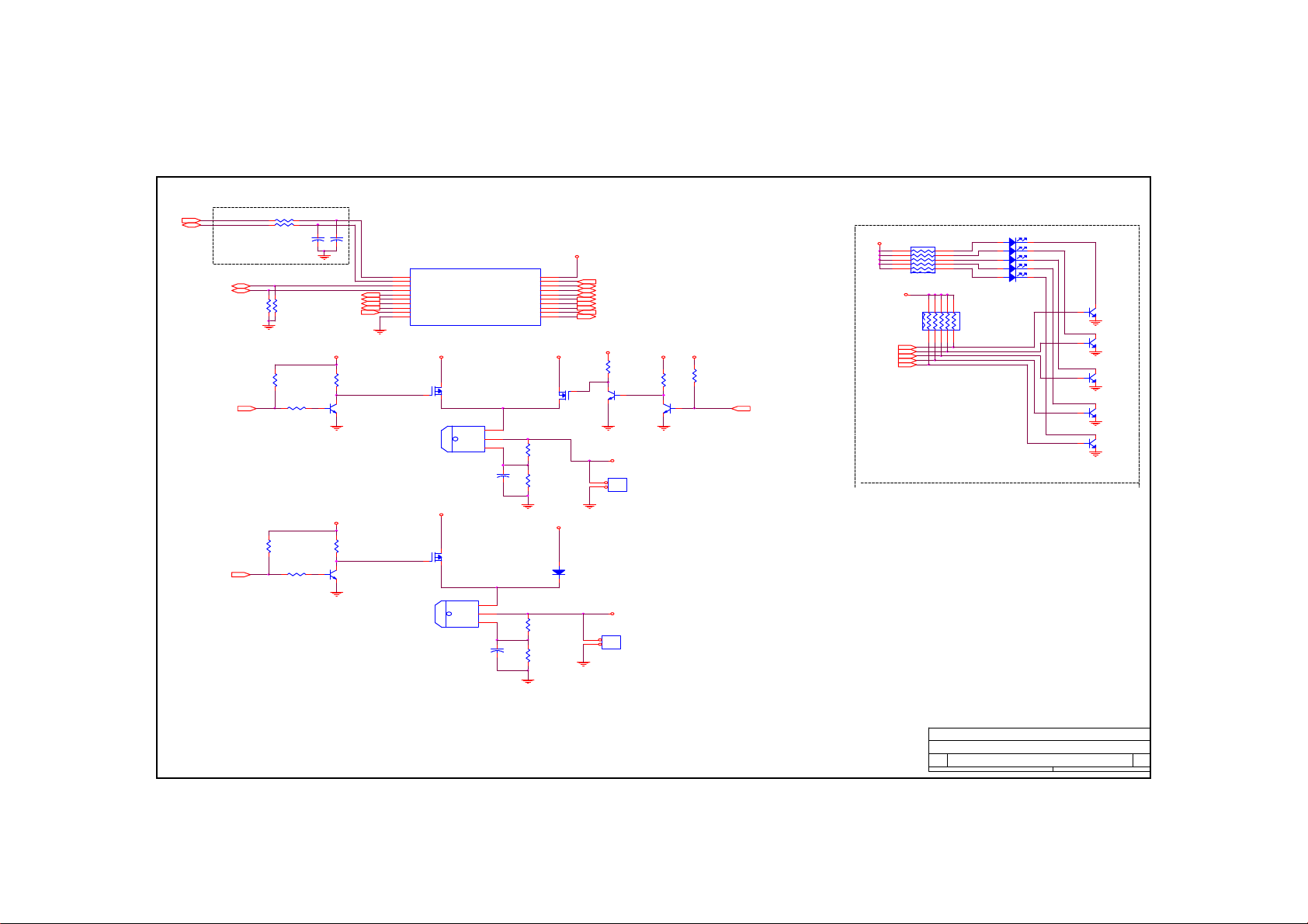
W83602R Example Application Circuit
Reserved for needed
R1
10K
GP22
R16
1K
GP23
R10
R9
C1
C2
U2
1
SCLK
2
SDAT
3
GP20/A0
4
GP21/A1
5
GP22/A2/CTL3VSB
6
GP10
7
GP11
8
GP23/CTLSTRV
9
GP24/S5IN#
10
VSS
W83601R/602R
SMBus Address 30
Q1
G G
PMOS IRF9531
5VSB
G
GP26/INT/PWCTLIN#
5VSB 5VSB
D
S
U1
LT1084_M
S
U3
LT1084_M
D
Q6
PMOS IRF9531
VOUT
3
VIN
2
VOUT
1
ADJ
3
VIN
2
1
ADJ
5VSB
5VSB
CTL3VSB
CTLSTRV
SLP_S5#
GP10
GP11
Q4
NPN 3904
Q7
NPN 3904
R11
4.7K
R17
4.7K
R2
10K
R10
1K
R13
330
R18
330
SCL
SDA
Note 1.
CTLSTRV
CTL3VSB
GP20
GP21
GP17/INT
GP25/PS_ON#
C7
CAP
5VSB
20
VCC
19
RST#
18
17
GP16
16
GP15
15
GP14
14
GP13
13
GP12
12
11
NMOS H603AL
R14
R
R15
C6
R
CAP
5VCC
R20
R
R21
R
PCIRST#
GP17
GP16
GP15
GP14
GP13
GP12
PWRCTL#
PS_ON#
5VCC 5VCC
S
D
12VCC
Q3
Q2
NPN 3904
JP10
1
2
HEADER2
D17
1N5817
JP13
1
2
HEADER2
From W83627F/HF power control
To Power Supply PS_ON# signal
R8
4.7K
VCC3_3VSB
VRAM
This reset signal can be from
system reset or GPO signal
R9
1K
R12
4.7K
Q5
NPN 3904
From system power good signal.
This signal should be +5V high level.
VRAM voltage is for RAM module VCC.
PWRGOOD
Diagnostic LEDs
VCC
R12
1 10
2 9
3 8
4 7
5 6
100
VCC
Pull-up
resistors
GP10
GP11
GP12
GP13
GP14
D1
D2
D3
D4
D5
11029384756
R11
4.7K
Q9
2N3904
Q10
2N3904
Q11
2N3904
Q12
2N3904
Q13
2N3904
Note 1. : Be sure that during Power-On reset or RST# reset,
GP20 and GP21 will not receive signal which will affect
the SMBus address setting.
Winbond Electronic Corp.
Title
W83602R Example Application Circuit
Size Document Number Rev
602ap.sch 0.1
Custom
Date: Sheet of
1 1Thursday, August 12, 1999
Page 17
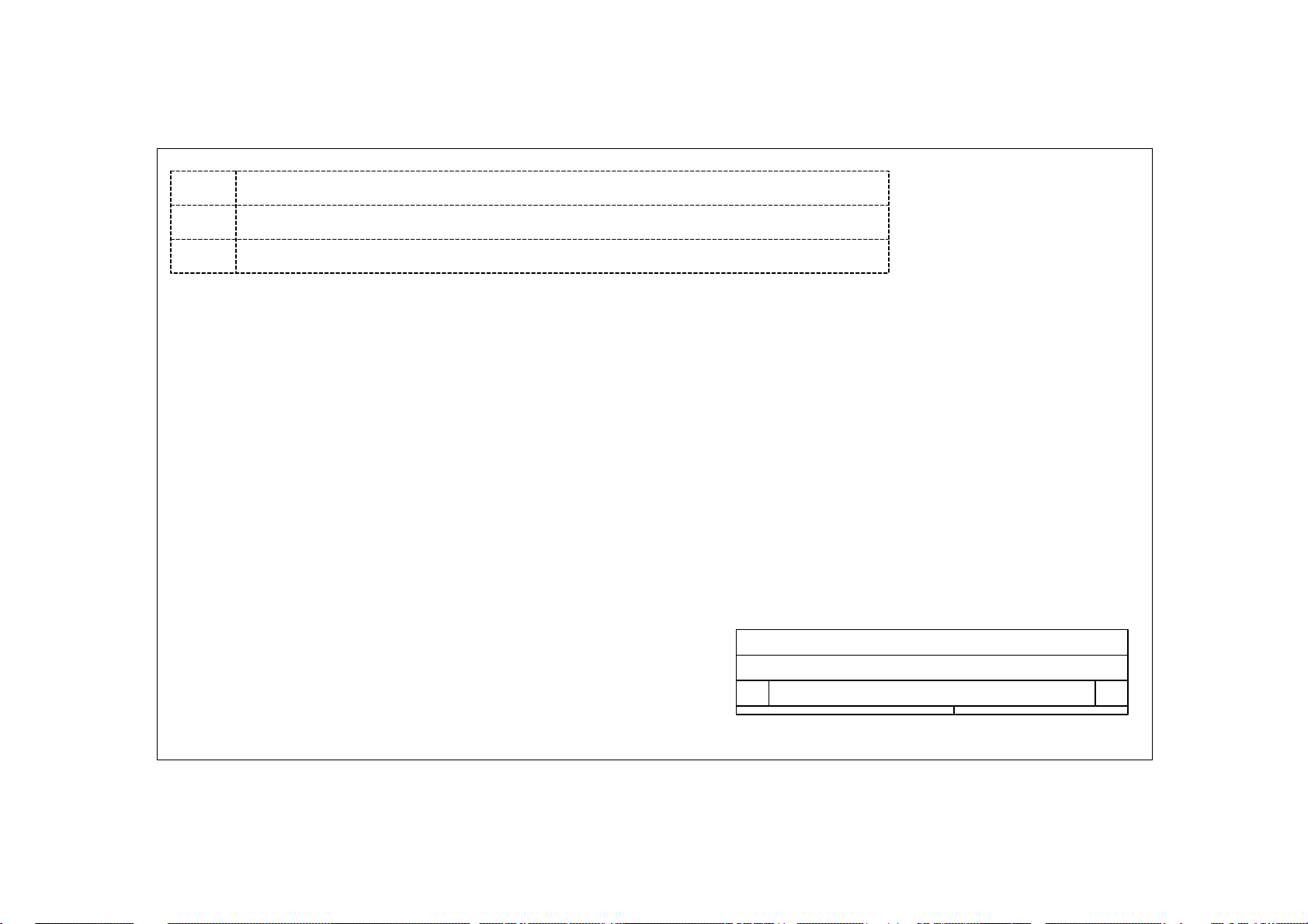
REV
0.1
0.2
Decription
First Publication
Change CTL3VSB, CTLSTRV Schematic
Winbond Electronic Corp.
Title
W83601R/602R Example Application Circuit
Size Document Number Rev
Custom
Date: Sheet of
602ap.sch 0.2
2 1Friday, August 13, 1999
 Loading...