

Page 1

W83301R
Winbond
ACPI-STR Controller
Page 2
W83301R
Data Sheet Revision History
Pages Dates Version
1 N.A. 01/Feb. 0.5 N.A. All of the versions before 0.50 are for internal use.
2 4,5 01/MAY 0.6 N.A. Application circuit Update
Please note that all data and specifications are subject to change without notice. All the
trademarks of products and companies mentioned in this datasheet belong to their
respective owners.
LIFE SUPPORT APPLICATIONS
These products are not designed for use in life support appliances, devices, or systems
where malfunction of these products can reasonably be expected to result in personal
injury. Winbond customers using or selling these products for use in such applications do
so at their own risk and agree to fully indemnify Winbond for any damages resulting from
such improper use or sales.
Version
on Web
Main Contents
Page 3

W83301R
Preliminary
1. General Description
The W83301R is an ACPI-compliant controller for microprocessor and other
computer applications. In substance, the part can mainly operate in alternative
configurations mode A and B – mode A provides a switch controller to generate a 5VDL
voltage from ATX power supply, a linear controller – STR1 (2.5V
termination controller – 1.25 V
for high speed bus such as RDRAM/DDRAM
DUAL
current sinking and sourcing; and mode B provides a switch controller to generate a
5VDL voltage from ATX power supply and three linear controllers for specific voltage
regulations – that is STR1 (2.5V
outputs can simply configured by V
), STR2 (3.3V
DUAL
SET0
, V
) and STR3 (1.8 V
DUAL
. Besides, the W83301R also can
SET1
provide extra voltage up to 0.2V in each regulator output for more performance. In
order to reduce the customer’s cost, and simplify the circuit design, the W83301R
integrates a charge-pump engine into the chip to provide higher driving voltage for
single N-channel MOSFETs, that is the W83301R, can drive only N-channel
MOSFETs for all applications. In the other hand, the W83301R also offer PWOK and
over current detection to protect each output and soft-start protects all linear
controllers from rush current attack. The W83301R is available in a 20-pin SOP
package.
), and a bus
DUAL
), all of the
DUAL
2.Features
Provides alternative configurations for flexible applications
Mode A
Provide a switch controller to generate 5V
Linear controller STR1–2.5V
Bus termination controller –1.25V
(RDRAM/DDRAM application)
DUAL
for high speed bus termination
DUAL
application to sinking and sourcing redundant current
Mode B
Provide a switch controller to generate 5V
Linear controller STR1 – 2.5V
Linear controller STR2 – 3.3 V
Linear controller STR3 – 1.8V
(Clock Gen. Application)
DUAL
(SDRAM Application)
DUAL
(Chipset Application)
DUAL
Provide a switch to enable/disable 5VDL output in S5 state via 5V
application
Supports SDRAM/RDRAM/DDRAM ACPI-STR Functions
Drives all N-Channel MOSFETs
Power-Up Softstart for all controllers
Up to 0.2V incremental voltage on STR1/STR2 for over-clock application.
Under-Voltage Fault Monitor
DUAL
DUAL
pin for USB
DLEN
Soft-Start function
20-Pin SOP Package
Confidential
Revision 0.6
1
Page 4
W83301R
Preliminary
3.Pin Configuration
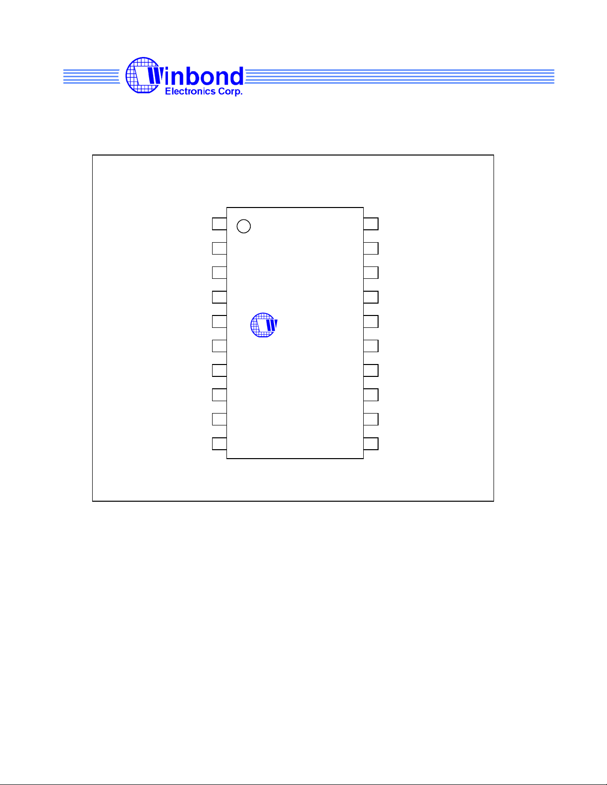
Figure 1. W83301R Pin Configuration
STR
STR
DRV2
SEN2
/BT
/BT
DRV
SEN
STR
DRV3
/BT
SINK
STR
SEN3
Vss
Vcc
C1
C2
ChrPmp
5VDLEN#
inbond
W83301R
STR
DRV1
STR
SEN1
SS
PWOK
5V
DRV
5V
DLSB
V
SET0
V
SET1
S3#
S5#
Confidential
Revision 0.6
2
Page 5
W83301R
Preliminary
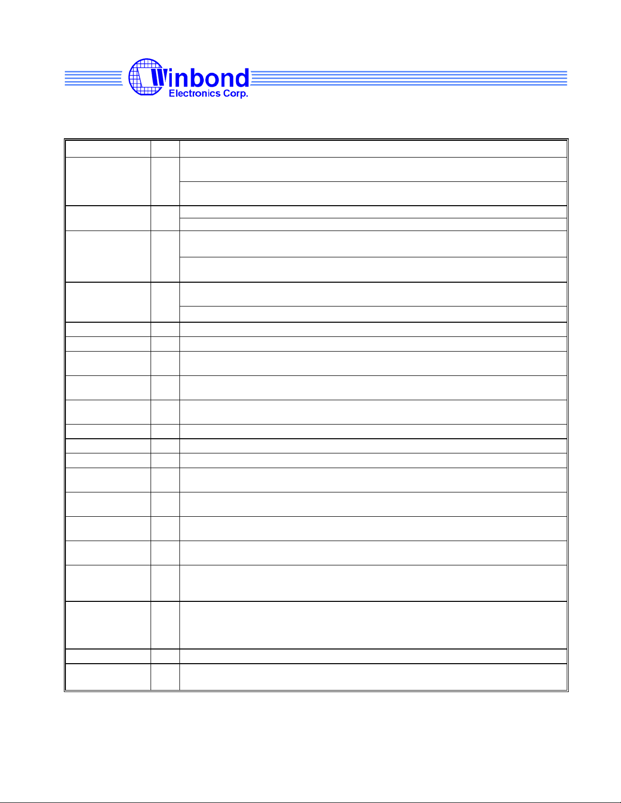
4.Pin Description
SYMBOL PIN FUNCTION
Mode A: BT Current Source. Connect this pin to the gate of a suitable N-channel
STR
DRV2
/BT
1
DRV
MOSFET for driving bus termination regulator output.
Mode B: STR2 Driver. Connect this pin to the gate of a suitable N-channel
MOSFET for driving STR2 output.
STR
SEN2
/BT
2
SEN
Mode A: BT Sense. Connect this pin to the bus termination regulator output.
Mode B: STR2 Sense. Connect this pin to the STR2 output.
Mode A: BT Current Sink. This pin is used to drive a N-channel MOSFET to sink
STR
DRV3
/BT
3
SINK
the redundant current in the high-speed bus.
Mode B: STR3 Driver. Connect this pin to the gate of a suitable N-channel
MOSFET for driving STR3 output.
Mode A: Function Reserved. Pull up this pin to +5VSB through a 1.5 Kohm
STR
4
SEN3
resistor.
Mode B: STR3 Sense. Connect this pin to the STR3 output.
GND 5
Vcc 6
C1 7
C2 8
ChrPmp 9
5V
# 10
DLEN
S5# 11
S3# 12
V
13
SET1
V
14
SET0
5V
15
DLSB
5V
16
DRV
Power Ground. Connect this pin to ground.
Power Vcc. Input 5VSB supply.
Charge Pump Cap. Attach flying capacitor between this pin and C2 to generate
internally used high voltage from 5V power supply.
Charge Pump Cap. Attach flying capacitor between this pin and C1 to generate
internally used high voltage from 5V power supply.
Charge Pump output. This pin produces voltage doubled 5V supply by charge-
pumping. Bypass with a 0.1uF capacitor.
5VDL Enable. Control 5V
voltage output. Pull-up internally.
DL
S5 Status. Control signal governing the soft off state S5. Pull-up internally.
S3 Status. Control signal governing the soft off state S3. Pull-up internally.
Voltage Selection 1. Combine with VSET2 to select operation mode and output
voltages of STR regulators.
Voltage Selection 0. Combine with VSET1 to select operation mode and output
voltages of STR regulators.
5VSB Output Control. Connect this pin to the gate of a N-MOSFET to output
5VSB power to 5V
DL
.
5V Output Control. Connect this pin to the gate of a N-MOSFET to output 5V
power to 5V
DL
.
Power OK. Open collector input/output. Used to indicate the ready of 5Vin supply. If
PWOK 17
any STR supply (only STR1 in mode A) occurs over current and induce undervoltage, PWOK will be pull down.
Soft-Start. Attach a capacitor (0.033u) to this pin to determine the softstart rate. A
SS 18
ramp generated by charging this capacitor with internal soft-start current (18uA) is
used to clamp the voltage rising slew rate of STR regulators and 5V
. Soft starting
DL
avoids too much rush current during voltage setup.
STR
STR
19
SEN1
20
DRV1
STR1 Sense. Connect this pin to the STR1 output.
STR1 Driver. Connect this pin to the gate of a suitable N-channel MOSFET for
driving STR1 output.
Confidential
Revision 0.6
3
Page 6
5. Application Circuit
5VSB
Q3
MOSFET N
W83301R
Preliminary
C1
0.1u
3.3Vdual
5V
6
5VSB
STRdrv1
STRsen1
STRdrv2
20
19
1
3.3Vdual
Q2
MOSFET N
U1
16
5VDRV
15
5VDLSB
Q1
MOSFET N
Q4
MOSFET N
C2
0.1u
C4
0.1u
C3
1000u
2.5V
2
0.1u
STRsen2
3
STRdrv3
R1
4
STRsen3
ChrPmp
C2
9
8
C9
0.1u
1.5k
(chipset)
C5
1000u
PWOK
5VDLEN
S3
SLP_S5#
VSET1
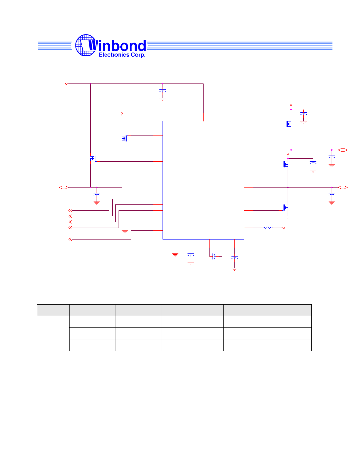
Connect VSET0 and VSET1 as following table to
set operation mode and output voltage
17
PWOK
10
5VDLEN
12
S3
11
S5
14
VSET0
13
VSET1
C7
0.1u
C1
7
C8
SS
GND
18
5
Figure 2. Mode A (DDR Mode) Application Circuit
Mode VSET0 VSET1 STR1 Bus Termination Controller
DDR
0V 0V 2.5V
0V NC 2.6V
0V 5V 2.7V
1.25V
DUAL
1.30V
DUAL
1.35V
DUAL
DUAL
DUAL
DUAL
5VSB
Q5
MOSFET N
C6
1000u
1.25V5VDUAL
Confidential
4
Revision 0.6
Page 7
W83301R
Preliminary
5. Application Circuit
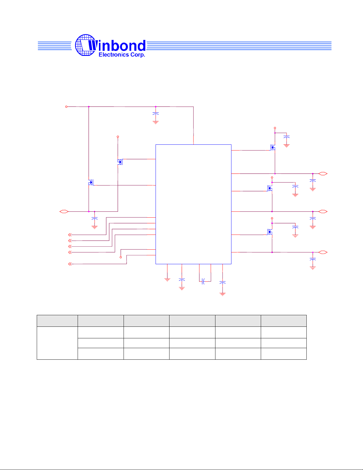
Figure 3. Mode B (SDRAM Mode) Application Circuit
5VSB
(chipset)
Q3
MOSFET N
5VDUAL
C5
1000u
PWOK
5VDLEN
S3
SLP_S5#
VSET1
Connect VSET0 and VSET1 as fol lowing tabl e
to set operation mode and output voltage
5V
5VSB
Q2
MOSFET N
C1
0.1u
3.3Vdual
C2
0.1u
6
U1
16
5VDRV
15
5VDLSB
17
PWOK
10
5VDLEN
12
S3
11
S5
14
VSET0
13
VSET1
GN
D
5
5VS
B
SS
18
C9
0.1u
C2
C1
8
7
C10
0.1u
STRdrv1
STRsen1
STRdrv2
STRsen2
STRdrv3
Chr
STRsen3
Pm
p
9
20
19
1
2
3
4
C11
0.1u
5VDUAL
3.3Vdual
Q1
MOSFET N
Q4
MOSFET N
Q5
MOSFET N
2.5V
C3
1000u
C6
1000u
C8
1000u
3.3V
1.8V
C4
0.1u
C7
0.1u
Mode VSET0 VSET1 STR1 STR2 STR3
SDRAM
5V 5V 2.5V
5V NC 2.6V
5V 0V 2.7V
3.3V
DUAL
3.4V
DUAL
3.5V
DUAL
1.8V
DUAL
1.8V
DUAL
1.8V
DUAL
DUAL
DUAL
DUAL
Confidential
Revision 0.6
5
Page 8
6.Block Diagram
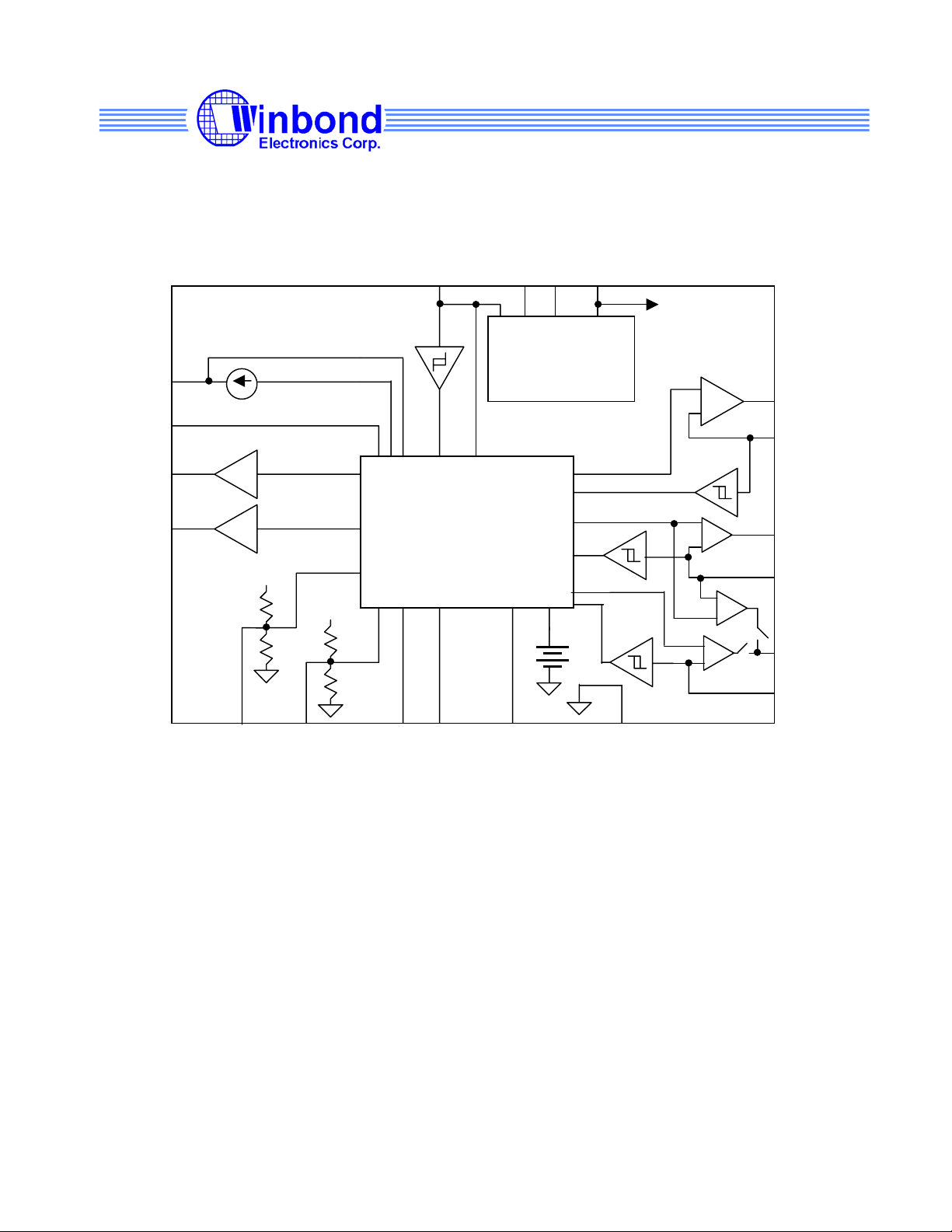
Figure 4. W83301R Internal Block Diagram
SS
5V
DRV
5V
DLSB
+5VSB
+5VSB
VSET0
VSET1
Vcc C1 C2 ChrPmp
Monitor
and
Control
S3# S5#
5V
Charge Pump
1.26V
#
DLEN
GND
W83301R
Preliminary
To
POWMOS
drivers
STR
STR
STR
STR
STR
STR
DRV1
SEN1
DRV2
SEN2
DRV3
SEN3
/BT
/BT
/BT
DRV
SEN
SINK
Confidential
6
Revision 0.6
Page 9
W83301R
Preliminary
7.Functional Description
7.1 Mode Selection
The W83301R supports two modes for customer’s multi-applications, as shown as
Table1, the mode A and mode B can selected via VSET0 pin. If this pin connects to 5V,
the chip will operate under mode A, otherwise the chip will operate under mode B when
VSET0 connects to ground.
Both mode A and B supports a linear switch to generate an ACPI-compliant 5VDL
voltage from ATX power supply 5V/5VSB according to S5# and S3# signals. And user
also can turn off the whole 5VDL output in S5 state via 5V
Under the mode A operation, the chip provide a linear controller STR1 that drives a
N-channel MOSFET Q3 (refer to figure) to generate a regulated voltage 2.5V
external power source 3.3V
, the 2.5 V
DUAL
is provide for RDRAM/DDRAM ACPI
DUAL
suspend to RAM application. And In order to simply the circuit design and reduce
customer’s cost, the W83301R also integrate a bus termination controller BT driving two
external N-channel MOSFETs (Q4, Q5) to generate a specific ACPI-compliant voltage
according to a half of STR1 output for sourcing and sinking bus redundant current.
# pin if needed.
DLEN
DUAL
from an
Under the mode B operation, the chip provide three linear controllers, that is STR1-
2.5V
, STR2- 3.3 V
DUAL
, and STR3- 1.8V
DUAL
, all of the three outputs drive a N-
DUAL
channel MOSFET (Q3, Q4, and Q5) to generate an ACPI-compliant voltage by different
applications. Such as STR1- 2.5V
for SDRAM application, and STR3- 1.8V
for clock generator application, STR2- 3.3 V
DUAL
chipset application.
DUAL
DUAL
Besides, as shown in Table 1 the W83301R also provide a tri-state pin VSET1 to bias
an extra voltage up to 0.2V in each output for more performance but under mode A
operation, the BT output voltage will generated according to a half of STR1 output set by
VSET1.
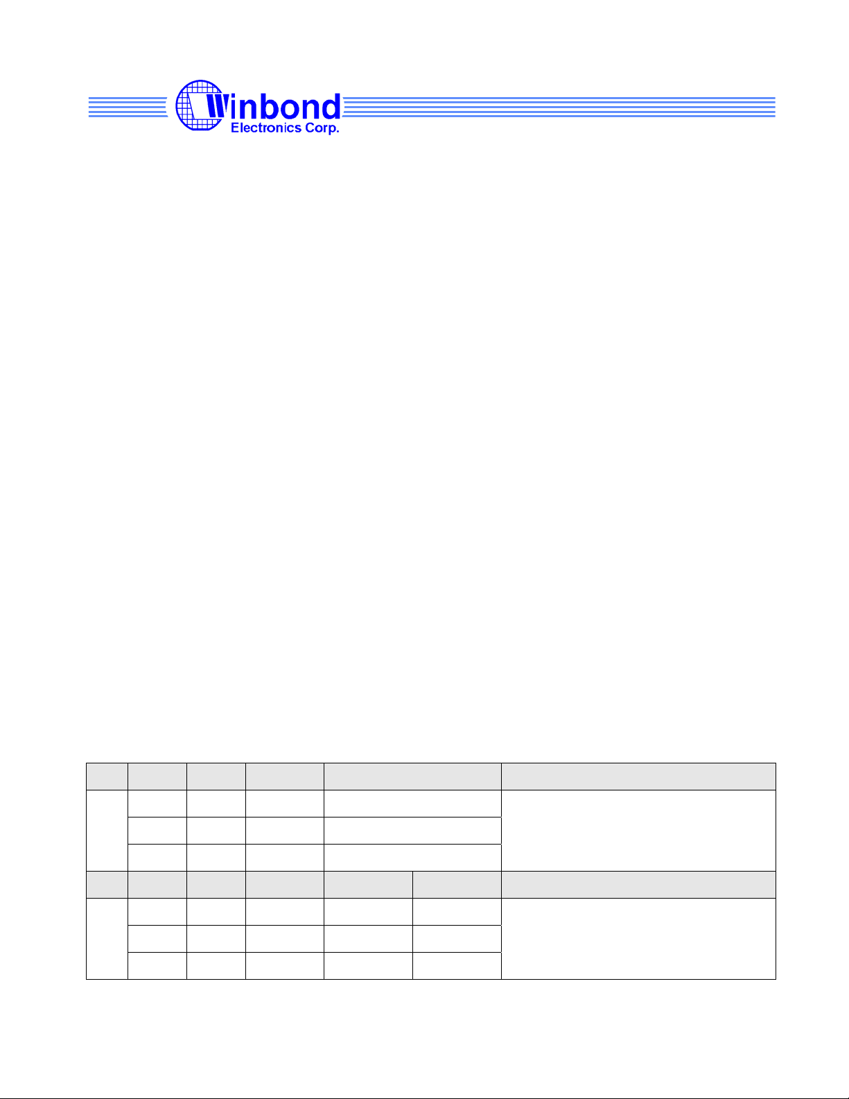
Table 1. W83301R Control Table
Mode VSET0 VSET1 STR1 Bus Termination Controller Remark
0V 0V 2.5V
A
Mode VSET0 VSET1 STR1 STR2 STR3 Remark
B
0V NC 2.6V
0V 5V 2.7V
5V 5V 2.5V
5V NC 2.6V
5V 0V 2.7V
1.25V
DUAL
1.30V
DUAL
1.35V
DUAL
3.3V
DUAL
3.4V
DUAL
3.5V
DUAL
1.8V
DUAL
1.8V
DUAL
1.8V
DUAL
DUAL
DUAL
DUAL
DUAL
DUAL
DUAL
-STR1 output for RDRAM/DDRAM voltage
-Bus Termination Controller for memory bus
redundant current sinking and sourcing.
-STR1 output for Clock Gen. voltage
-STR2 output for SDRAM voltage
-STR3 output for Chipset voltage
Confidential
Revision 0.6
7
Page 10
W83301R
Preliminary
7.2 ACPI State Control
In order to meet the ACPI specification, the W83301R implement a state machine as
shown as Figure 5 to generate ACPI-compliant power state transition.
There are only five states in the state machine cause the W83301R only focus on the
memory ACPI control, and the five states are G3 (Mechanical-Off State), S0 (Full-Power
State), S3 (Sleeping State-Suspend to RAM), S5
states changed to the other according to the condition of S3#, S5# and 5V
other hand, cause of the W83301R allows customer to disable/enable the 5V
in S5 state via 5V
# pin, there are two states, S5On and S5
DLEN
state. A soft ramp-up mechanism is needed to protect the 5VDL output from the rush
current attack during the S5
to S5On state transition. Same as the 5VDL output, the
Off
W83301R also provides soft ramp-up mechanism during S5
each STR output.
In the state machine, when the power on, and the 5V input from power supply arrive
4.5V, the chip will enter S5
conditions, the one is when 5V
first from G3, and ramp-up into S5On state by two
Off
#=0 under standby power supply to resume the 5VDL
DLEN
output, the other one is S3#=1 and S5#=1 the system will enter S1 state.
(Soft-Off State), S5
On
On
and all of these
Off
#. On the
DLEN
output
DUAL
, corresponding to S5
Off
to S0 state transition in
During S5On state, the chip will return back to S5
disabling the 5VSB output (5V
#=1) to save some power. And the chip will drive all
DLEN
when the customer wants
Off
outputs into S0 state will S3#=1 and S5#=1.
When the system under the S0 state, the system should enter the S3-sleeping
(S3#=0, S5#=1) or S5-soft off (S5#=0) state when the system idle for a long time or user
power-off.
When the system suspend to RAM, the system will be wakeup and enter S0-full
power state by (S3#=1, S5#=1,PWOK=1), or get into S5-sleeping soft off state by
(S5#=0)
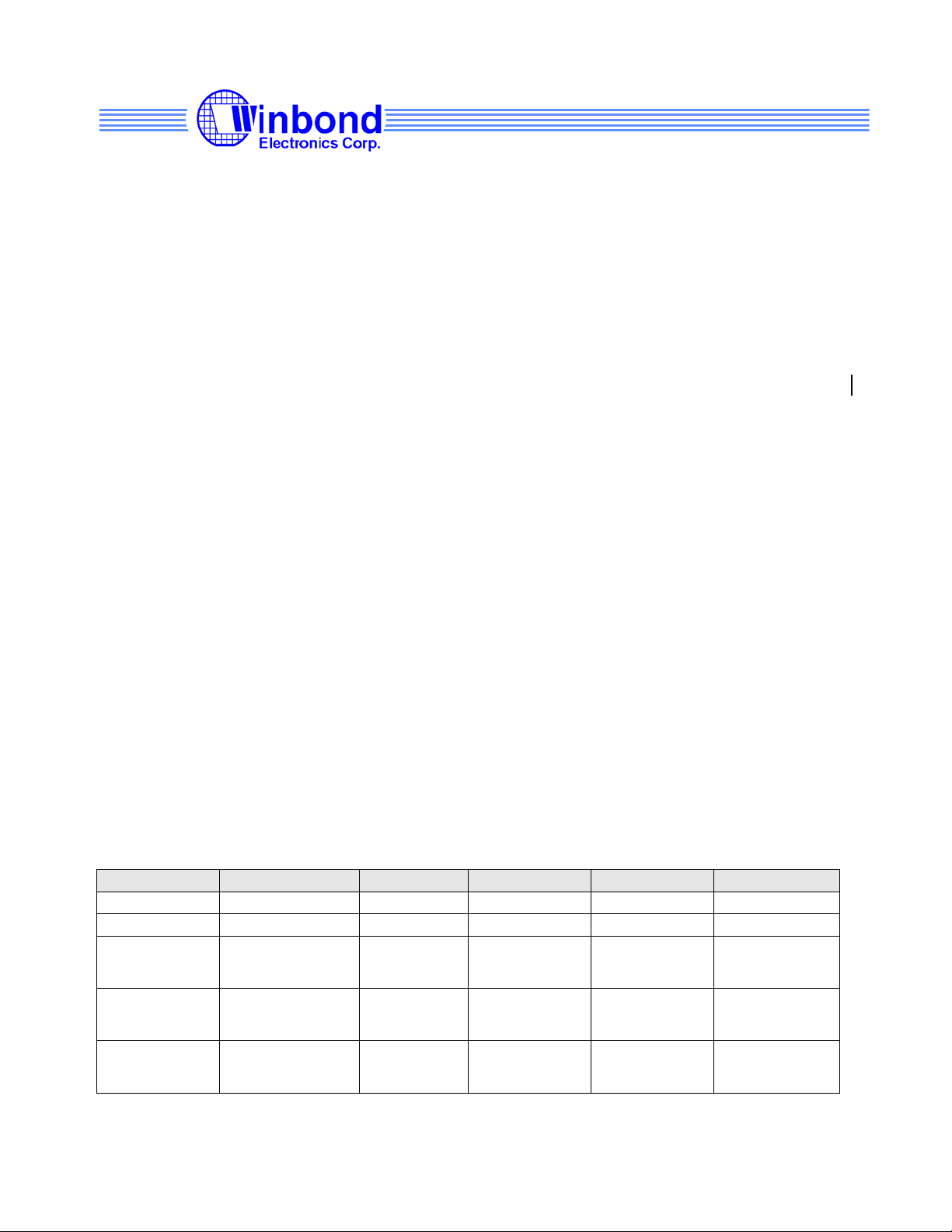
Table 2. W83301R Outputs Table
State 5VDL STR1 STR2 STR3 LUV Activity *
G3 Off Off Off Off No
S5 (5VDL Off) Off Off Off Off No
On
S5 (5VDL On)
(Driven by
5V
DLSB
)
Off Off Off No
On
S0
(Driven by
5V
DRV
)
On On On Yes
On
S3
*When the STR2 & STR3 configured as bus termination controller, only STR1 has linear under voltage
function.
(Driven by
5V
DLSB
)
On On On Yes
Confidential
Revision 0.6
8
Page 11

W83301R
Preliminary
7.3 Charge Pump
In order to simply the design circuit and provide a good-price solution for customer,
the W83301R integrate with a switched-capacitor voltage doubler charge pump to
provide a higher driving voltage (Up to 10 volt) and can drive a single N-channel
MOSFETs in each output.
7.4 Power OK
The W83301R use a bi-direction Power OK signal to ensure the system can work
normally. When the system jump from state S3 to state S0, the W83301R will monitor the
input signal from PWOK pin to ensure that external system power is OK and then switch
each outputs into S0 stage; In the other hand, the W83301R will pull down the Power OK
signal to inform the system that a over current and induce under-voltage occurred.
7.5 Soft-Start
During ‘S5off’ to ‘S5on’ and ‘S5on’ to ‘S0’ state transitions, the 5Vdual and STR
voltages need to ramp up from 0 to their set values respectively. The charging current
flowing to output capacitors must be limited to avoid supply drop-off.
In W83301R, an internal 18 uA current source (Iss) charges an external capacitor
(Css) to generate a linear ramp-up voltage on SS pin (Vss). The Vss slews from 0 to
about 9V during the above-mentioned state transitions, and the Vss slew rate is used to
clamp the ramp-up rate of 5Vdual and STR output voltages. This output clamping allows
power-ups free of supply drop-off events.
Since the outputs are ramped up in a constant slew-rate, the current dedicated to
charge any output capacitor can be calculated with the following formula:
I
= Iss x (Cout / Css)
COUT
Some technique is included in W83301R to further reduce the total charging current:
In Mode B configuration, the start-up of ramp-up time STR3 (1.8V) will be advanced from
that of STR1 to reduce the overlap time of charging. And in Mode A configuration, the
bus-terminator is input clamped, and its output voltage slew-rate, so as its charging
current, will be limited to half of that of STR1.
Note that, too slow ramp-up rate is not recommended. If so, the state transition
mentioned above will be prolonged to much. Before Vss ramps up to its upper limit
(about 9V), the state transition will not be completed and will not go into next state.
Confidential
Revision 0.6
9
Page 12
W83301R
Preliminary
8.Electrical Characteristics
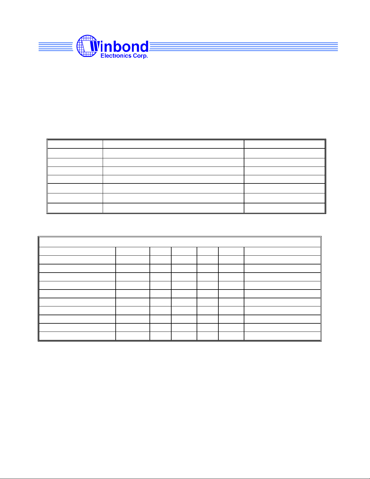
8.1 ABSOLUTE MAXIMUM RATINGS
Stresses greater than those listed in this table may cause permanent damage to the
device. Precautions should be taken to avoid application of any voltage higher than the
maximum rated voltages to this circuit. Subjection to maximum conditions for extended
periods may affect reliability. Unused inputs must always be tied to an appropriate logic
voltage level (Ground or Vdd).
Symbol Parameter Rating
Vss, Vcc
ChrPmp - 0.5 V to + 12.0 V
Hi-V Pins Pin# 1,2,3,4,8,15,16,18,19,20 GND-0.3 V to V
Lo-V Pins Pin# 7,10,11,12,13,14,17 GND-0.3 V to Vcc + 0.3V
T
STG
TB
TA
Voltage on any pin with respect to GND - 0.5 V to + 7.0 V
+ 0.3V
Chr-Pmp
Storage Temperature
Ambient Temperature
Operating Temperature
- 65°C to + 150°C
- 55°C to + 125°C
0°C to + 70°C
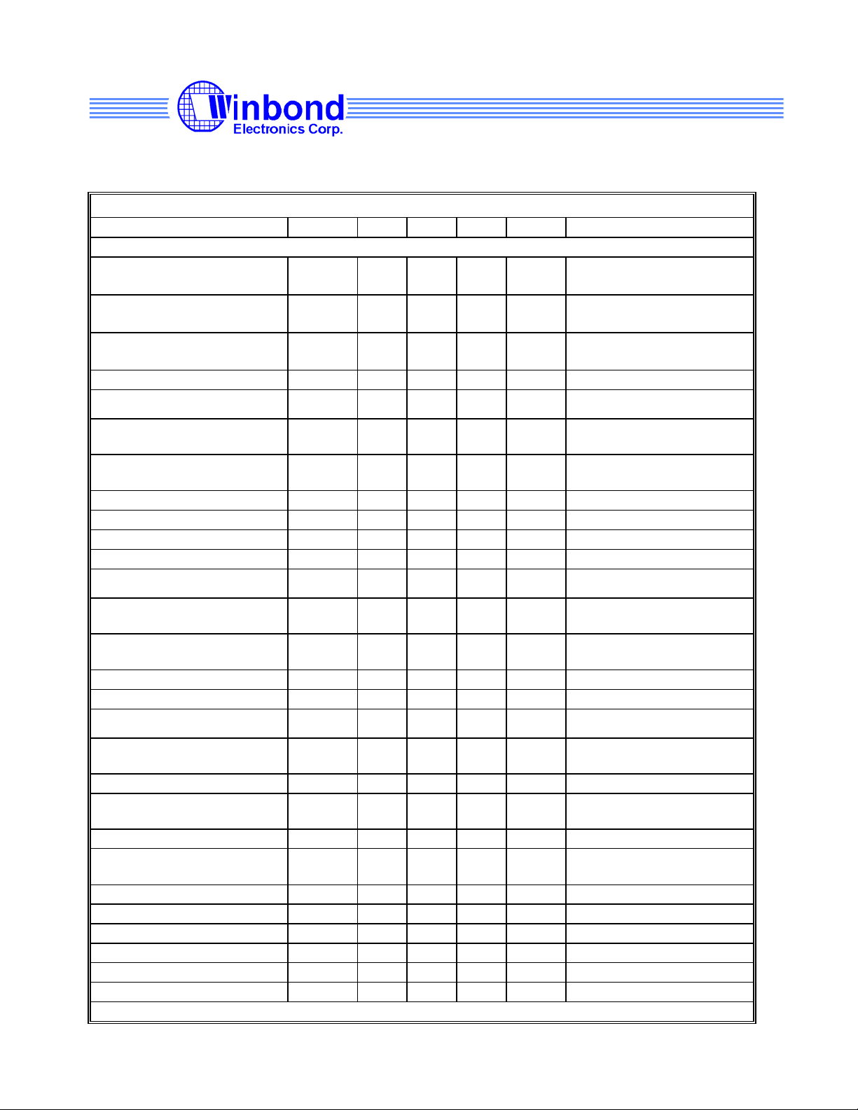
8.2 AC CHARACTERISTICS
Vcc=5V ± 5 %, TA = 0°C to +70°C
Parameter Symbol Min Typ Max Units Test Conditions
Vcc SUPPLY CURRENT
Norminal Supply Current
POWER-ON RESET
Rising V
5VSB Hysteresis 1 V
Rising V
V
Chr_Pmp
SOFT-START
Soft-Start Current Iss
VSS upper limit
Threshold 4.3 V V
5VSB
Threshold 8.5 V V
Chr_Pmp
Hysteresis
I
5VSB
6 mA
Chr_Pmp
5VSB
1 V
18 uA
9 V
> 8.5V
> 4.3V
Confidential
Revision 0.6
10
Page 13
W83301R
Preliminary
8.2 AC CHARACTERISTICS (Continued)
Vcc=5V ± 5 %, TA = 0°C to +70°C
Parameter Symbol Min Typ Max Units Test Conditions
STR1 lINEAR REGULATOR
Nominal Output Voltage
Nominal Output Voltage
Nominal Output Voltage 2.8 V VSET0=0V, VSET1=5V
Regulation 5 %
STR
Under-Voltage Falling
SEN1
Threshold
MAX STR
DRV1
Output
6 V I(STR
Voltage
STR2 LINEAR
REGULATOR
Nominal Output Voltage
Nominal Output Voltage
Nominal Output Voltage 3.5 V VSET0=5V,VSET1=0V
Regulation 5 %
STR
Under-Voltage Falling
SEN1
Threshold
MAX STR
DRV1
Output
6 V I(STR
Voltage
STR3 LINEAR
REGULATOR
Nominal Output Voltage
Regulation 5 %
STR
Under-Voltage Falling
SEN1
Threshold
MAX STR
DRV1
Output
6 V I(STR
Voltage
BUS TERMINATOR
Nominal Output Voltage /
V
STRSEN1
Regulation 5 %
5VDUAL SWITCH
CONTROLLER
5V
Output High Voltage 9 Cload=3000p
DRV
5V
Sourcing Current 7 mA Cload=3000p
DRV
5V
Sinking Current 400 uA Cload=3000p
DRV
5V
Output High Voltage 9 Cload=3000p
DLSB
5V
Sourcing Current 7 mA Cload=3000p
DLSB
5V
Sinking Current 230 uA Cload=3000p
DLSB
S3#,S5#,5VDLEN#, PWOK,CHARGE PUMP
2.5 V VSET0=0V, VSET1=0V
or VSET0=5V,VSET1=5V
2.6 V VSET0=0V, VSET1=NC
or VSET0=5V,VSET1=NC
or VSET0=5V,VSET1=0V
80 %
) < 0.1mA
DRV1
3.3 V VSET0=5V,VSET1=5V
3.4 V VSET0=5V,VSET1=NC
80 %
) < 0.1mA
DRV1
1.8 V VSET0=5V
83 %
) < 0.1mA
DRV1
50 % VSET0=0V
Confidential
11
Revision 0.6
Page 14
Input Logic High 2.2 V
Input Logic Low 0.8 V
PWOK Output Inpedence 150 ohm LUV active
Charge Pump Frequency 200 KHz
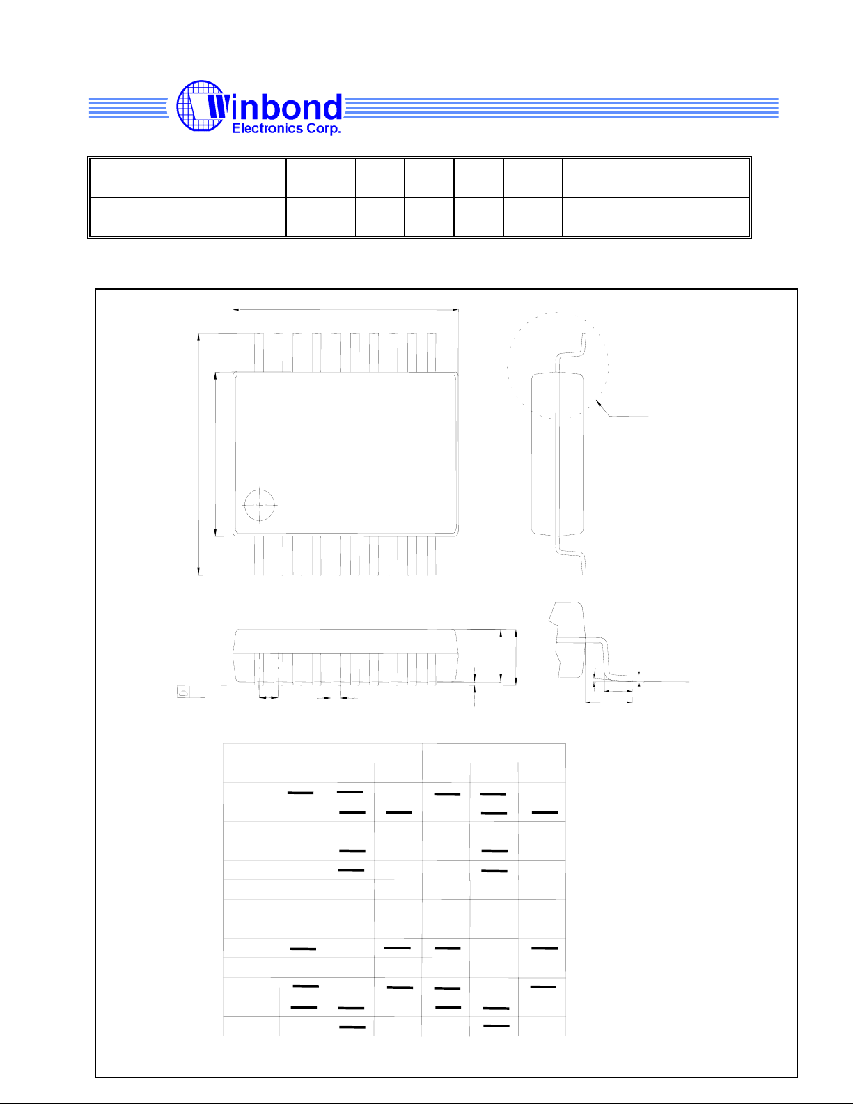
9.Package Specification
20L SSOP-209 mil
H
E
E
20
D
11
W83301R
Preliminary
DTEAIL A
Confidential
Revision 0.6
SEATING PLANE
Y
SYMBO
A
A1
A2
b
c
D
E
H
e
L
L1
Y
q
1
e
DIMENSION IN
MIN NO MAX.
0.05
1.65
0.22
0.09
6.90
5.00
E
7.40
0.55 0.75
0
b
1.75
7.20
5.30
7.80
0.65
1.25
0.38
0.25
7.50
5.60
8.20
0.10
2.00
1.85
0.95
8
10
DIMENSION IN
MIN
0.002
0.065
0.009
0.004
0.272
0.197
0.291
0.021 0.030
12
b
SEATING PLANE
L
L1
A1
NO
A2
A
DETAIL A
MAX.
0.079
q
0
0.069
0.283
0.209
0.307
0.025
0.050
0.073
0.015
0.010
0.295
0.220
0.323
0.037
0.004
8
Page 15

W83301R
Preliminary
Confidential
Revision 0.6
13
Page 16
10.Ordering Information
Part Number Package Type Production Flow
W83301R 20-PIN SSOP
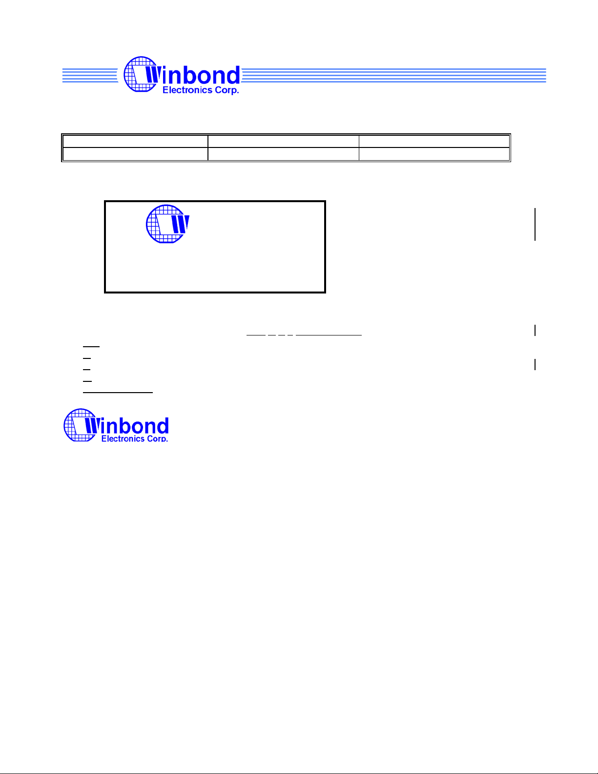
11.How to Read the Top Marking
1060B11039050-21NA
1st line: Winbond logo
2nd line: W883301R – the part number
3rd line: Tracking code Tracking code 106
: packages made in Year 01’, week 6
106
: assembly house ID; O means OSE, G means GR, …
O
: the IC version
A
wafers manufactured in Winbond FAB I
1:
1039050-21NA:
wafer production series number
inbond
W83301R
O B 1 1039050-21NA
W83301R
Preliminary
Commercial, 0°C to +70°C
Headquarters
No. 4, Creation Rd. III
Science-Based Industrial Park
Hsinchu, Taiwan
TEL: 886-35-770066
FAX: 886-35-789467
www: http://www.winbond.com.tw/
Taipei Office
11F, No. 115, Sec. 3, Min-Sheng East Rd.
Taipei, Taiwan
TEL: 886-2-7190505
FAX: 886-2-7197502
TLX: 16485 WINTPE
Winbond Electronics (H.K.) Ltd.
Rm. 803, World Trade Square, Tower II
123 Hoi Bun Rd., Kwun Tong
Kowloon, Hong Kong
TEL: 852-27516023-7
FAX: 852-27552064
Winbond Electronics
(North America) Corp.
2730 Orchard Parkway
San Jose, CA 95134 U.S.A.
TEL: 1-408-9436666
FAX: 1-408-9436668
Please note that all data and specifications are subject to change without notice. All the trade
marks of products and companies mentioned in this data sheet belong to their respective owners.
These products are not designed for use in life support appliances, devices, or systems where
malfunction of these products can reasonably be expected to result in personal injury. Winbond
customers using or selling these products for use in such applications do so at their own risk and
agree to fully indemnify Winbond for any damages resulting from such improper use or sale.
Confidential
Revision 0.6
14
 Loading...