

Datasheet W78E58M-40, W78E58M-24, W78E58M-16, W78E58F-40, W78E58F-24 Datasheet (Winbond Electronics)
...Page 1

W78E58
INT2
INT2
8-BIT MICROCONTROLLER
GENERAL DESCRIPTION
The W78E58 is an 8-bit microcontroller that is functionally compatible with the W78C58, except that
the mask ROM is replaced by a flash EEPROM with a size of 32 KB. To facilitate programming and
verification, the flash EEPROM inside the W78E58 allows the program memory to be programmed
and read electronically. Once the code is confirmed, the user can protect the code for security.
The W78E58 microcontroller supplies a wider frequency range than most 8-bit microcontrollers on the
market. It is functionally compatible with the industry-standard 80C52 microcontroller series, except
that one extra 4-bit bit-addressable I/O port(Port 4) and two additional external interrupts (
INT3 ).
The W78E58 contains four 8-bit bi-directional and bit-addressable I/O ports, three 16-bit
timer/counters, and a serial port. These peripherals are supported by a eight-source, two-level
interrupt capability. There are 256 bytes of RAM and an 32 KB flash EEPROM for application
programs.
The W78E58 microcontroller has two power reduction modes, idle mode and power-down mode, both
of which are software selectable. The idle mode turns off the processor clock but allows for continued
peripheral operation. The power-down mode stops the crystal oscillator for minimum power
consumption. The external clock can be stopped at any time and in any state without affecting the
processor.
,
FEATURES
• 8-bit CMOS microcontroller
• Fully static design
• Low standby current at full supply voltage
• DC-40 MHz operation
• 256 bytes of on-chip scratchpad RAM
• 32 KB electrically erasable/programmable EPROM
• 64 KB program memory address space
• 64 KB data memory address space
• Four 8-bit bidirectional ports
• One extra 4-bit bit-addressable I/O port, additional
(available on 44-pin PLCC/QFP package)
• Three 16-bit timer/counters
• One full duplex serial port
• Boolean processor
• Eight-source, two-level interrupt capability
• Built-in power management
• Code protection mechanism
• Packages:
− DIP 40: W78E58-16/24/40
− PLCC 44: W78E58P-16/24/40
− QFP 44: W78E58F-16/24/40
− TQFP 44: W78E58M-16/24/40
/ INT3
Publication Release Date: November 1997
- 1 - Revision A2
Page 2
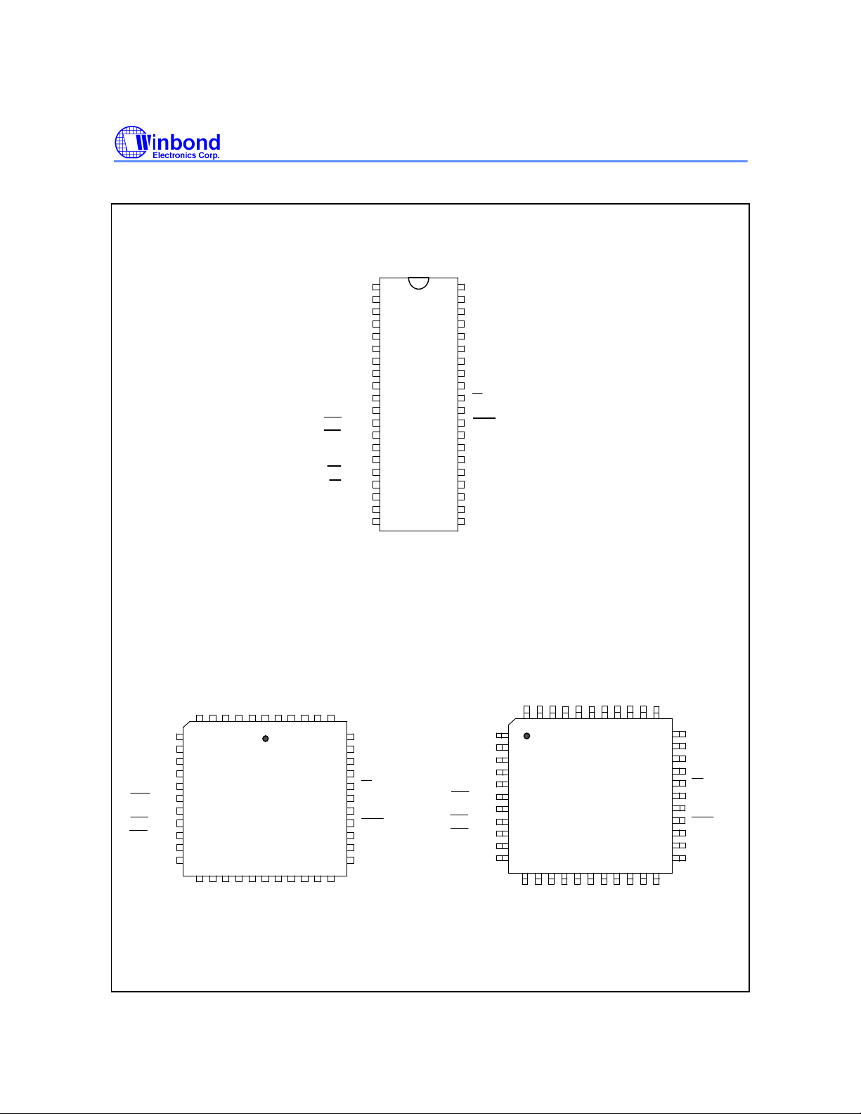
PIN CONFIGURATIONS
40-Pin DIP (W78E58)
T2, P1.0
T2EX, P1.1
P1.2
P1.3
P1.4
P1.5
P1.6
P1.7
RST
RXD, P3.0
TXD, P3.1
INT0, P3.2
INT1, P3.3
T0, P3.4
T1, P3.5
WR, P3.6
RD, P3.7
XTAL2
XTAL1
VSS
W78E58
VCC1
2
3
4
5
6
7
8
9
10
11
12
13
14
15
16
17
18
19
20
40
39
P0.0, AD0
38
P0.1, AD1
37
P0.2, AD2
36
P0.3, AD3
P0.4, AD4
35
34
P0.5, AD5
33
P0.6, AD6
P0.7, AD7
32
31
EA
30
ALE
29
PSEN
28
P2.7, A15
27
P2.6, A14
26
P2.5, A13
25
P2.4, A12
24
P2.3, A11
23
P2.2, A10
P2.1, A9
22
21
P2.0, A8
44-Pin PLCC (W78E58P)
T
2
T
E
2
X
,
,
P
P
P
P
P1.5
P1.6
P1.7
RST
RXD, P3.0
INT2, P4.3
TXD, P3.1
INT0, P3.2
INT1, P3.3
T0, P3.4
T1, P3.5
P
1
.
4
6 5 4 3
7
8
9
10
11
12
13
14
15
16
17
P
3
.
6
,
/
W
R
1
.
3
P
3
.
7
,
/
R
D
1
1
.
.
1
2
X
X
T
T
A
A
L
L
1
2
1
.
0
2 1 44 43 42
V
S
S
44-Pin QFP/TQFP (W78E58F/W78E58M)
/
P
1
.
4
P
3
.
6
,
/
W
R
P
P
1
1
.
.
2
3
43 42 41
X
P
T
3
A
.
L
7
2
,
/
R
D
T
I
2
N
T
E
T
2
X
3
,
,
,
P
P
P
1
1
4
.
.
.
0
1
2
403938 37 36
X
V
P
T
S
4
A
S
.
L
0
1
A
A
A
A
D
D
D
D
3
2
1
0
,
,
,
,
P
P
P
P
0
0
V
0
0
.
.
C
.
.
3
1
C
2
0
34
3544
P
P
P
P
2
2
2
2
.
.
.
.
3
1
0
2
,
,
,
,
A
A
A
A
1
1
9
8
1
0
P0.4, AD4
33
32
P0.5, AD5
31
P0.6, AD6
30
P0.7, AD7
29
EA
28
P4.1
27
ALE
26
PSEN
25
P2.7, A15
24
P2.6, A14
23
P2.5, A13
22212019181716151413
P
2
.
4
,
A
1
2
/
I
N
T
3
,
P
V
4
C
.
C
2
P
P
2
4
.
.
0
0
,
A
8
A
A
A
A
D
D
D
D
3
2
1
0
,
,
,
,
P
P
P
P
0
0
0
0
.
.
.
.
3
2
1
0
40
41
P
P
P
2
2
2
.
.
.
3
2
1
,
,
,
A
A
A
1
9
1
1
0
P0.4, AD4
39
38
P0.5, AD5
37
P0.6, AD6
36
P0.7, AD7
35
EA
34
P4.1
33
ALE
32
PSEN
31
P2.7, A15
30
P2.6, A14
29
P2.5, A13
2827262524232221201918
P
2
.
4
,
A
1
2
RXD, P3.0
INT2, P4.3
TXD, P3.1
INT0, P3.2
INT1, P3.3
T0, P3.4
T1, P3.5
P1.5
P1.6
P1.7
RST
1
2
3
4
5
6
7
8
9
10
11
12
- 2 -
Page 3
W78E58
INT2
PIN DESCRIPTION
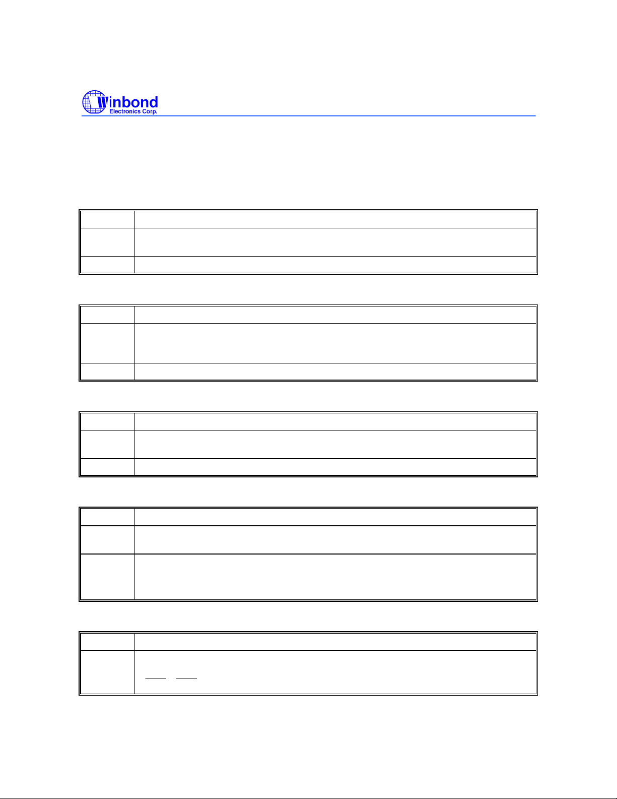
The W78E58 has two operating modes, normal and flash. In normal mode, the W78E58 corresponds
to the W78C58. In flash mode, the user (the maker of the flash EEPROM writer) can access the flash
EEPROM.
P0.7−P0.0 Port 0, Bits 7−0
MODE DESCRIPTION
Normal Port 0, Bits 0 through 7. Port 0 is a bidirectional I/O port. This port also provides a
multiplexed low order address/data bus during accesses to external memory.
Flash This port provides the data bus during access to the flash EEPROM.
P1.7−P1.0 Port 1, Bits 7−0
MODE DESCRIPTION
Normal Port 1, Bits 0 through 7. Port 1 is a bidirectional I/O port with internal pull-ups. Pins
P1.0 and P1.1 also serve as T2 (Timer 2 external input) and T2EX (Timer 2
capture/reload trigger), respectively.
Flash This port provides the low-order address bus during access to the flash EEPROM.
P2.7−P2.0 Port 2, Bits 7−0
MODE DESCRIPTION
Normal Port 2, Bits 0 through 7. Port 2 is a bidirectional I/O port with internal pull-ups. This port
also provides the upper address bits for accesses to external memory..
Flash This port provides the high-order address bus during access to the flash EEPROM.
P3.7−P3.0 Port 3, Bits 7−0
MODE DESCRIPTION
Normal Port 3, Bits 0 through 7. Port 3 is a bidirectional I/O port with internal pull-ups. All bits
have alternate functions.
Flash
P3.3−P3.0 and P3.7−P3.6 are the flash mode configuration pins, Input.
P3.3−P3.0 and P3.7−P3.6 are configured to select or execute the flash operations. For
details, see Flash Operations.
P4.3−P4.0 Port 4, Bits 3−0 (available on 44-pin PLCC/QFP package)
MODE DESCRIPTION
Normal Another bit-addressable bidirectional I/O port P4. P4.3 and P4.2 are alternative
function pins. It can be used as general I/O pins or external interrupt input sources
(
/ INT3 ).
Publication Release Date: November 1997
- 3 - Revision A2
Page 4
Flash No function in this mode.
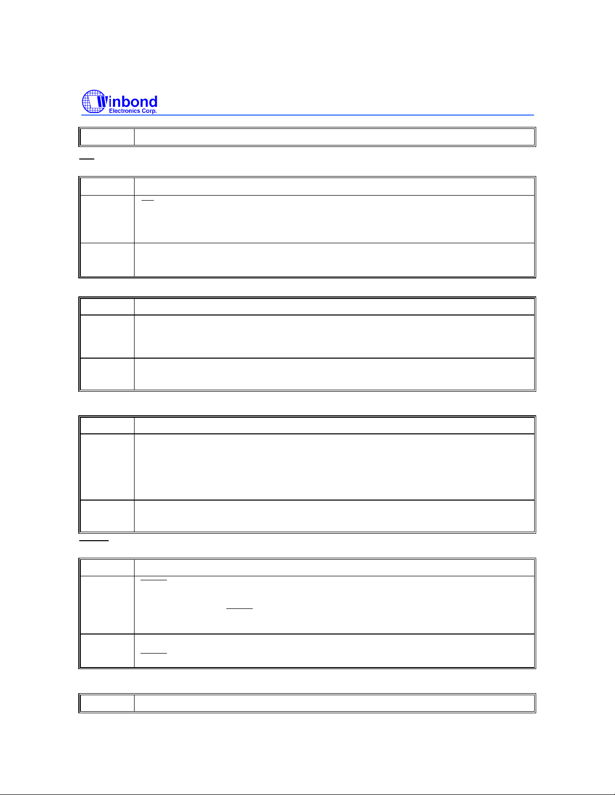
EA
PSEN
This pin
PSEN
PSEN
EA/VPP
MODE DESCRIPTION
W78E58
Normal
Flash VPP, Program Power supply pin, Input.
External Access, Input, active low.
,
This pin forces the processor to execute a program from the external ROM. When the
internal flash EEPROM is accessed as in the W78C58, this pin should be kept high.
This pin accepts the high voltage (12V) needed for programming the flash EEPROM.
RST
MODE DESCRIPTION
Normal RST, Reset, Input, active high.
This pin resets the processor. It must be kept high for at least two machine cycles in
order to be recognized by the processor.
Flash Flash mode configuration pin, Input, active high.
RST is used to configure the flash operations. For details, see Flash Operations.
ALE
MODE DESCRIPTION
Normal
Flash Flash mode configuration pin, Input, active low.
Address Latch Enable, Output, active high.
ALE,
ALE is used to enable the address latch that separates the address from the data on
Port 0. ALE runs at 1/6th of the oscillator frequency. A single ALE pulse is skipped
during external data memory accesses. ALE goes to a high impedance state with a
weak pull-up during reset state.
ALE is used to configure the flash operations. For details, see Flash Operations.
PSEN
MODE DESCRIPTION
Normal
MOVC operations.
reset state
Flash Flash mode configuration pin, Input, active high.
Program Store Enable, Output, active low.
,
enables the external ROM onto the Port 0 address/data bus during fetch and
goes to a high impedance state with a weak pull-up during
is used to configure the flash operations. For details, see Flash Operations.
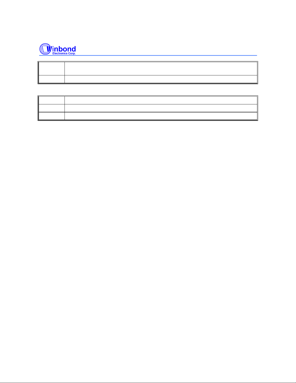
XTAL1
MODE DESCRIPTION
- 4 -
Page 5
W78E58
Normal Crystal 1. This is the crystal oscillator input. This pin may be driven by an external
clock.
Flash Connect to VSS.
XTAL2
MODE DESCRIPTION
Normal Crystal 2. This is the crystal oscillator output. It is the inversion of XTAL1.
Flash No function in this mode.
VSS, VCC
Power Supplies. These are the chip ground and positive supplies.
Publication Release Date: November 1997
- 5 - Revision A2
Page 6
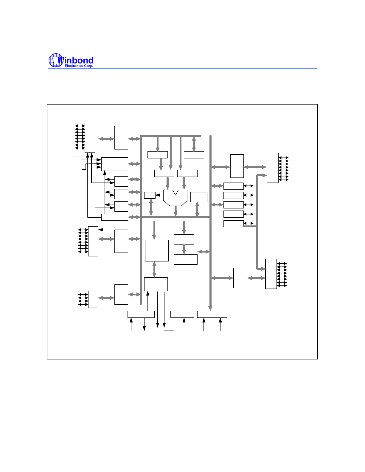
BLOCK DIAGRAM
P1.0
~
P1.7
Port
1
W78E58
Port 1
Latch
P3.0
~
P3.7
P4.0
~
P4.3
INT2
INT3
Port
Port
T2
SFR RAM
Address
256 bytes
RAM & SFR
B
Stack
Pointer
Power Control
Port 0
Latch
DPTR
Temp Reg.
PC
Incrementor
Addr. Reg.
Port 2
Latch
Port
0
Port
2
P0.0
~
P0.7
P2.0
~
P2.7
ACC
Interrupt
PSW
Instruction
Decoder
&
Sequencer
Bus & Clock
Controller
T1
ALU
Reset Block
Timer
2
Timer
0
Timer
1
UART
3
4
Port 3
Latch
Port 4
Latch
Oscillator
XTAL1
XTAL2
ALE
PSEN
RST
- 6 -
VssVcc
Page 7

W78E58
FUNCTIONAL DESCRIPTION
The W78E58 architecture consists of a core controller surrounded by various registers, five general
purpose I/O ports, 256 bytes of RAM, three timer/counters, and a serial port. The processor supports
111 different opcodes and references both a 64K program address space and a 64K data storage
space.
Timers 0, 1, and 2
Timers 0, 1, and 2 each consist of two 8-bit data registers. These are called TL0 and TH0 for Timer 0,
TL1 and TH1 for Timer 1, and TL2 and TH2 for Timer 2. The TCON and TMOD registers provide
control functions for timers 0 and 1. The T2CON register provides control functions for Timer 2.
RCAP2H and RCAP2L are used as reload/capture registers for Timer 2.
The operations of Timer 0 and Timer 1 are the same as in the W78C51. Timer 2 is a special feature
of the W78E58: it is a 16-bit timer/counter that is configured and controlled by the T2CON register.
Like Timers 0 and 1, Timer 2 can operate as either an external event counter or as an internal timer,
depending on the setting of bit C/T2 in T2CON. Timer 2 has three operating modes: capture, autoreload, and baud rate generator. The clock speed at capture or auto-reload mode is the same as that
of Timers 0 and 1.
Clock
The W78E58 is designed to be used with either a crystal oscillator or an external clock. Internally, the
clock is divided by two before it is used. This makes the W78E58 relatively insensitive to duty cycle
variations in the clock.
Crystal Oscillator
The W78E58 incorporates a built-in crystal oscillator. To make the oscillator work, a crystal must be
connected across pins XTAL1 and XTAL2. In addition, a load capacitor must be connected from each
pin to ground, and a resistor must also be connected from XTAL1 to XTAL2 to provide a DC bias
when the crystal frequency is above 24 MHz.
External Clock
An external clock should be connected to pin XTAL1. Pin XTAL2 should be left unconnected. The
XTAL1 input is a CMOS-type input, as required by the crystal oscillator. As a result, the external clock
signal should have an input one level of greater than 3.5 volts.
Power Management
Idle Mode
The idle mode is entered by setting the IDL bit in the PCON register. In the idle mode, the internal
clock to the processor is stopped. The peripherals and the interrupt logic continue to be clocked. The
processor will exit idle mode when either an interrupt or a reset occurs.
Power-down Mode
When the PD bit of the PCON register is set, the processor enters the power-down mode. In this
mode all of the clocks are stopped, including the oscillator. The only way to exit power-down mode is
by a reset.
Publication Release Date: November 1997
- 7 - Revision A2
Page 8

W78E58
INT2
INT2
Reset
The external RESET signal is sampled at S5P2. To take effect, it must be held high for at least two
machine cycles while the oscillator is running.
An internal trigger circuit in the reset line is used to deglitch the reset line when the W78E58 is used
with an external RC network. The reset logic also has a special glitch removal circuit that ignores
glitches on the reset line.
During reset, the ports are initialized to FFH, the stack pointer to 07H, PCON (with the exception of
bit 4) to 00H, and all of the other SFR registers except SBUF to 00H. SBUF is not reset.
Option Setting
Users write programs into the W78E58 by using the Winbond proprietary writer. The writer programs
the data into an internal 32 KB region and reads the data back for verification. After confirming that
the program is correct, the user can lock the data so that they can no longer be read.
Lock Bit
This bit is used to protect the customer data in the W78E58. It may be turned on after the
programmer finishes the programming and verify sequence. Once this bit is set to logic 0, no flash
data can be accessed again.
MOVC Execute
This bit is used to restrict the region accessible to the MOVC instruction. It can prevent the program
from being downloaded using this instruction if the program needs to jump outside to get data. When
this bit is set to logic 0, a MOVC instruction in external program memory space will be able to
access code in the external memory, but it will not be able to access code in the internal memory. A
MOVC instruction in internal program memory space will always be able to access code in both
internal and external memory. If this bit is logic 1, there are no restrictions on the MOVC instruction.
New Defined Peripheral
In order to be more suitable for I/O, an extra 4-bit bit-addressable port P4 and two external interrupt
, INT3 has been added to either the PLCC or QFP 44 pin package. And description follows:
1. INT2/INT3
Two additional external interrupts,
interrupt 0 and 1 in the standard 80C52. The functions/status of these interrupts are
determined/shown by the bits in the XICON (External Interrupt Control) register. The XICON register
is bit-addressable but is not a standard register in the standard 80C52. Its address is at 0C0H. To
set/clear bits in the XICON register, one can use the "SETB (/CLR) bit" instruction. For example,
"SETB 0C2H" sets the EX2 bit of XICON.
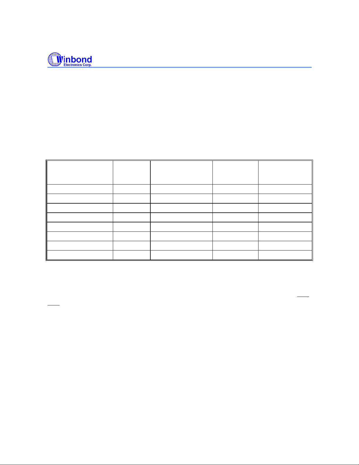
***XICON - external interrupt control (C0H)
PX3 EX3 IE3 IT3 PX2 EX2 IE2 IT2
and INT3 , whose functions are similar to those of external
PX3: External interrupt 3 priority high if set
- 8 -
Page 9
W78E58
INT2
EX3: External interrupt 3 enable if set
IE3: If IT3 = 1, IE3 is set/cleared automatically by hardware when interrupt is detected/serviced
IT3: External interrupt 3 is falling-edge/low-level triggered when this bit is set/cleared by software
PX2: External interrupt 2 priority high if set
EX2: External interrupt 2 enable if set
IE2: If IT2 = 1, IE2 is set/cleared automatically by hardware when interrupt is detected/serviced
IT2: External interrupt 2 is falling-edge/low-level triggered when this bit is set/cleared by software
Eight-source interrupt informations:
INTERRUPT
SOURCE
External Interrupt 0 03H 0 (highest) IE.0 TCON.0
Timer/Counter 0 0BH 1 IE.1 External Interrupt 1 13H 2 IE.2 TCON.2
Timer/Counter 1 1BH 3 IE.3 Serial Port 23H 4 IE.4 Timer/Counter 2 2BH 5 IE.5 External Interrupt 2 33H 6 XICON.2 XICON.0
External Interrupt 3 3BH 7 (lowest) XICON.6 XICON.3
2. PORT4
Another bit-addressable port P4 is also available and only 4 bits (P4<3:0>) can be used. This port
address is located at 0D8H with the same function as that of port P1, except the P4.3 and P4.2 are
alternative function pins. It can be used as general I/O pins or external interrupt input sources (
INT3 ).
Example:
P4 REG 0D8H
VECTOR
ADDRESS
POLLING
SEQUENCE WITHIN
PRIORITY LEVEL
ENABLE
REQUIRED
SETTINGS
INTERRUPT
TYPE
EDGE/LEVEL
/
MOV P4, #0AH ; Output data "A" through P4.0−P4.3.
MOV A, P4 ; Read P4 status to Accumulator.
SETB P4.0 ; Set bit P4.0
CLR P4.1 ; Clear bit P4.1
3. Reduce EMI Emission
Because of the large on-chip flash EEPROM, when a program is running in internal ROM space, the
ALE will be unused. The transition of ALE will cause noise, so it can be turned off to reduce the EMI
Publication Release Date: November 1997
- 9 - Revision A2
Page 10
W78E58
PSEN
emission if it is useless. Turning off the ALE signal transition only requires setting the bit 0 of the
AUXR SFR, which is located at 08Eh. When ALE is turned off, it will be reactivated when the program
accesses external ROM/RAM data or jumps to execute an external ROM code. The ALE signal will
turn off again after it has been completely accessed or the program returns to internal ROM code
space..
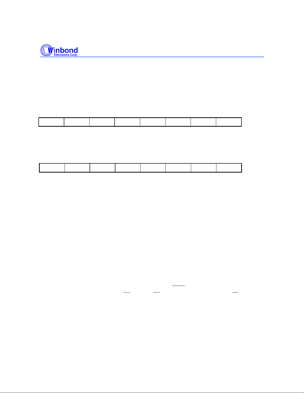
The AO bit in the AUXR register, when set, disables the ALE output.
***AUXR - Auxiliary register (8EH)
- - - - - - - AO
AO: Turn off ALE output.
4. Power-off Flag
***PCON - Power control (87H)
SMOD - - POF GF1 GF0 PD IDL
SMOD: Double baud rate bit. When set to a 1, the baud rate is doubled when the serial port is
being used in either modes 1, 2, 3.
POF: Power off flag. Bit is set by hardware when power on reset. It can be cleared by software
to determine chip reset is a warm boot or cold boot.
GF1, GF0: These two bits are general-purpose flag bits for the user.
PD: Power down mode bit. Set it to enter power down mode.
IDL: Idle mode bit. Set it to enter idle mode.
The power-off flag is located at PCON.4. This bit is set when VDD has been applied to the part. It can
be used to determine if a reset is a warm boot or a cold boot if it is subsequently reset by software.
Flash Operations
In normal operation, the W78E58 is functionally compatible with the W78C58. In the flash operating
mode, the flash EEPROM can be programmed and verified repeatedly. Once the code inside the
flash EEPROM is confirmed, the code can be protected. The flash EEPROM and the operations on it
are described below.
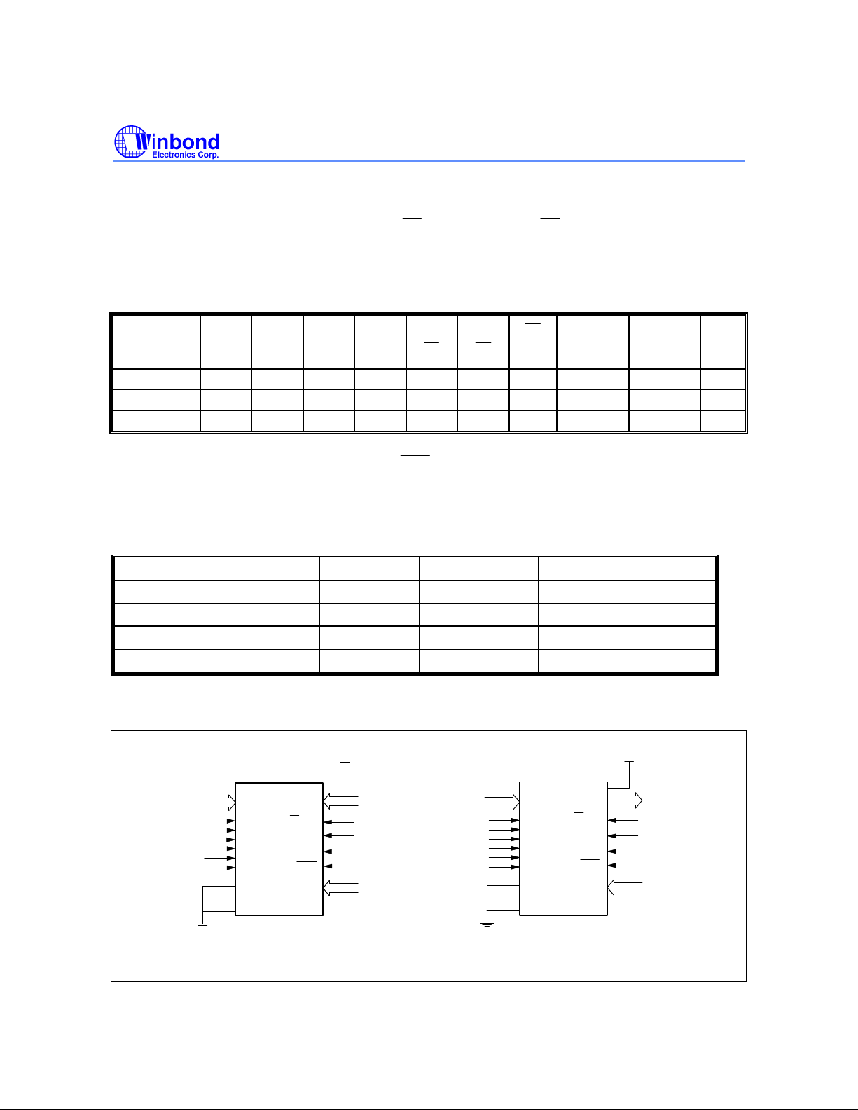
All of the operations are configured by the pins RST, ALE,
A14CTRL (P3.2), OECTRL (P3.3), CE (P3.6), OE (P3.7), A0 (P1.0) and VPP (EA). In these
operations, A15 to A0 (P2.7 to P2.0, P1.7 to P1.0) and D7 to D0 (P0.7 to P0.0) serve as the address
and data bus, respectively.
Read Operation
This operation enables customers to read their codes and the option bits. The data will not be valid if
the lock bit is programmed to low.
- 10 -
, A9CTRL (P3.0), A13CTRL (P3.1),
Page 11
W78E58
PSEN
Program Operation
This operation is used to program data to the flash EEPROM and the option bits. Programming is
initiated when VPP reaches VCP (12.5V) level, CE is set to low, and OE is set to high.
Program Verify Operation
All data must be checked after programming. This operation should be performed after each byte is
programmed, and it will ensure a substantial program margin.
OPERATION P3.0
(A9
CTRL)
Read VIL VIL VIL VIL VIL VIL VIH
Program VIL VIL VIL VIL VIL VIH VCP
Program Verify VIL VIL VIL VIL VIH VIL VCP
Notes:
1. During all of these operations, RST = VIH, ALE = VIL, and
2. VCP = 12V, VIH = VDD, VIL = Vss.
3. The program verify operation should follow the programming operaion.
P3.1
(A13
CTRL)
P3.2
(A14
CTRL)
P3.3
(OE
CTRL)
P3.6
( CE )
= VIH.
P3.7
( OE )
EA
(VPP)
P2, P1
(A15 TO A0)P0(D7 TO D0)
Address Data Out 1, 2
Address Data In 1, 2
Address Data Out 3
NOTES
ABSOLUTE MAXIMUM RATINGS
PARAMETER SYMBOL MIN. MAX. UNIT
DC Power Supply
VDD−VSS
Input Voltage VIN VSS -0.3 VDD +0.3 V
Operating Temperature TA 0 70
Storage Temperature TST -55 +150
Note: Exposure to conditions beyond those listed under Absolute Maximum Ratings may adversely affect the life and reliability of
the device.
+5V
V
A0 to A7
P1
V
IL
V
IL
V
IL
V
IL
V
IL
V
IH
P3.0
P3.1
P3.2
P3.3
P3.6
P3.7
X'tal1
X'tal2
Vss
DD
P0
EA/Vpp
ALE
RST
PSEN
P2
PGM DATA
V
CP
V
IL
V
IH
V
IH
A8 to A15
-0.3 +7.0 V
+5V
V
A0 to A7
P1
V
IL
V
IL
V
IL
V
IL
V
IH
V
IL
P3.0
P3.1
P3.2
P3.3
P3.6
P3.7
X'tal1
X'tal2
Vss
DD
P0
EA/Vpp
ALE
RST
PSEN
P2
PGM DATA
V
CP
V
IL
V
IH
V
IH
A8 to A15
°C
°C
Programming Configuration
Programming Verification
Publication Release Date: November 1997
- 11 - Revision A2
Page 12
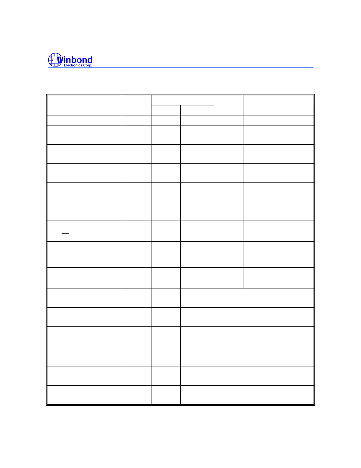
DC CHARACTERISTICS
EA
EA
EA
(VDD-VSS = 5V ±10%, TA = 25°C, Fosc = 20 MHz, unless otherwise specified.)
PARAMETER SYM. SPECIFICATION UNIT TEST CONDITIONS
MIN. MAX.
Operating Voltage VDD 4.5 5.5 V
Operating Current IDD - 20 mA No load
VDD = 5.5V
Idle Current IIDLE - 6 mA Idle mode
VDD = 5.5V
Power Down Current IPWDN - 50
Input Current
P1, P2, P3, P4
Input Current
RST
Input Leakage Current
P0,
Logic 1 to 0 Transition
Current
P1, P2, P3, P4
Input Low Voltage
IIN1 -50 +10
IIN2 -10 +300
ILK -10 +10
ITL [*4] -500 -200
VIL1 0 0.8 V VDD = 4.5V
µA
µA
µA
µA
µA
Power-down mode
VDD = 5.5V
VDD = 5.5V
VIN = 0V or VDD
VDD = 5.5V
0 < VIN < VDD
VDD = 5.5V
0V <VIN < VDD
VDD = 5.5V
VIN =2.0V
W78E58
P0, P1, P2, P3, P4,
Input Low Voltage
RST
Input Low Voltage
XTAL1[*4]
Input High Voltage
P0, P1, P2, P3, P4,
Input High Voltage
RST
Input High Voltage
XTAL1 [*4]
Output Low Voltage
P1, P2, P3, P4
VIL2 0 0.8 V VDD = 4.5V
VIL3 0 0.8 V VDD = 4.5V
VIH1 2.4 VDD +0.2 V VDD = 5.5V
VIH2 3.5 VDD +0.2 V VDD = 5.5V
VIH3 3.5 VDD +0.2 V VDD = 5.5V
VOL1 - 0.45 V VDD = 4.5V
IOL = +2 mA
- 12 -
Page 13
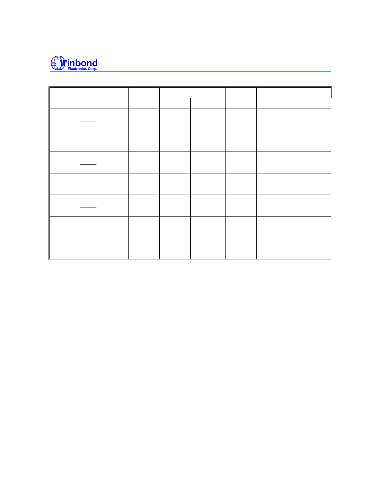
DC Characteristics, continued
PARAMETER SYM. SPECIFICATION UNIT TEST CONDITIONS
Output Low Voltage
P0, ALE, PSEN [*3]
W78E58
MIN. MAX.
VOL2 - 0.45 V VDD = 4.5V
IOL = +4mA
Sink Current
P1, P2, P3, P4
Sink Current
P0, ALE, PSEN
Output High Voltage
P1, P2, P3, P4
Output High Voltage
P0, ALE, PSEN [*3]
Source Current
P1, P2, P3, P4
Source Current
P0, ALE, PSEN
Notes:
*1. RST pin is a Schmitt trigger input. RST has internal pull-low resistors of about 30 KΩ.
*3. P0, ALE and /PSEN are tested in the external access mode.
*4. XTAL1 is a CMOS input.
*5. Pins of P1, P2, P3, P4 can source a transition current when they are being externally driven from 1 to 0. The transition
current reaches its maximum value when VIN approximates to 2V.
ISK1 4 12 mA VDD = 4.5V
Vs = 0.45V
ISK2 10 20 mA VDD = 4.5V
Vs = 0.45V
VOH1 2.4 - V VDD = 4.5V
IOH = -100 µA
VOH2 2.4 - V VDD = 4.5V
IOH = -400 µA
ISR1 -120 -250
µA
VDD = 4.5V
Vs = 2.4V
ISR2 -8 -14 mA VDD = 4.5V
Vs = 2.4V
AC CHARACTERISTICS
The AC specifications are a function of the particular process used to manufacture the part, the
ratings of the I/O buffers, the capacitive load, and the internal routing capacitance. Most of the
specifications can be expressed in terms of multiple input clock periods (TCP), and actual parts will
usually experience less than a ±20 nS variation. The numbers below represent the performance
expected from a 0.8 micron CMOS process when using 2 and 4 mA output buffers.
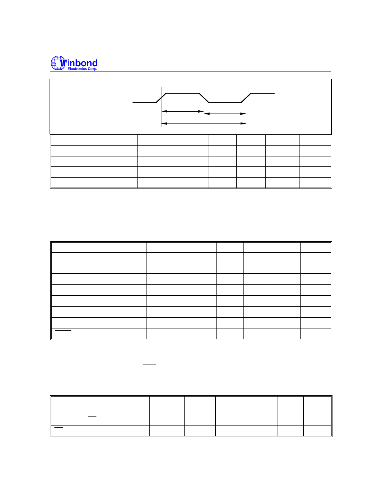
Clock Input Waveform
Publication Release Date: November 1997
- 13 - Revision A2
Page 14
W78E58
PSEN
PSEN
PSEN
PSEN
PSEN
PSEN
RD
XTAL1
T
CH
F
OP, TCP
T
CL
PARAMETER SYMBOL MIN. TYP. MAX. UNIT NOTES
Operating Speed FOP 0 - 40 MHz 1
Clock Period TCP 25 - - nS 2
Clock High TCH 10 - - nS 3
Clock Low TCL 10 - - nS 3
Notes:
1. The clock may be stopped indefinitely in either state.
2. The TCP specification is used as a reference in other specifications.
3. There are no duty cycle requirements on the XTAL1 input.
Program Fetch Cycle
PARAMETER SYMBOL MIN. TYP. MAX. UNIT NOTES
Address Valid to ALE Low TAAS
Address Hold from ALE Low TAAH
ALE Low to
Low to Data Valid
Data Hold after
Data Float after
Low
High
High
TAPL
TPDA - - 2 TCP nS 2
TPDH 0 - 1 TCP nS 3
TPDZ 0 - 1 TCP nS
ALE Pulse Width TALW
Pulse Width
TPSW
1 TCP -∆
1 TCP -∆
1 TCP -∆
2 TCP -∆
3 TCP -∆
- - nS 4
- - nS 1, 4
- - nS 4
2 TCP - nS 4
3 TCP - nS 4
Notes:
1. P0.0−P0.7, P2.0−P2.7 remain stable throughout entire memory cycle.
2. Memory access time is 3 TCP.
3. Data have been latched internally prior to
4. "∆" (due to buffer driving delay and wire loading) is 20 nS.
going high.
Data Read Cycle
PARAMETER SYMBOL MIN. TYP. MAX. UNIT NOTE
ALE Low to RD Low
Low to Data Valid
TDAR
TDDA - - 4 TCP nS 1
3 TCP -∆
- 14 -
S
-
3 TCP +∆
nS 1, 2
Page 15
W78E58
RD
WR
CE
CE
Data Hold from RD High
Data Float from RD High
Pulse Width
Notes:
1. Data memory access time is 8 TCP.
2. "∆" (due to buffer driving delay and wire loading) is 20 nS.
TDDH 0 - 2 TCP nS
TDDZ 0 - 2 TCP nS
TDRD
6 TCP -∆
6 TCP - nS 2
Data Write Cycle
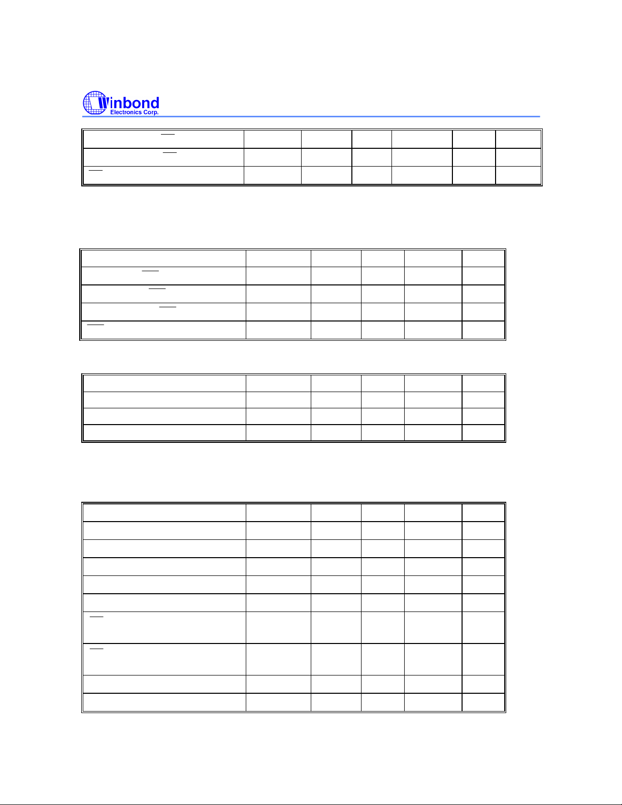
PARAMETER SYMBOL MIN. TYP. MAX. UNIT
ALE Low to WR Low
Data Valid to WR Low
Data Hold from WR High
Pulse Width
Note: "∆" (due to buffer driving delay and wire loading) is 20 nS.
TDAW
TDAD
TDWD
TDWR
3 TCP -∆
1 TCP -∆
1 TCP -∆
6 TCP -∆
-
3 TCP +∆
- - nS
- - nS
6 TCP - nS
Port Access Cycle
PARAMETER SYMBOL MIN. TYP. MAX. UNIT
Port Input Setup to ALE Low TPDS 1 TCP - - nS
Port Input Hold from ALE Low TPDH 0 - - nS
Port Output to ALE TPDA 1 TCP - - nS
nS
Note: Ports are read during S5P2, and output data becomes available at the end of S6P2. The timing data are referenced to
ALE, since it provides a convenient reference.
Program Operation
PARAMETER SYMBOL MIN. TYP. MAX. UNIT
VPP Setup Time TVPS 2.0 - Data Setup Time TDS 2.0 - Data Hold Time TDH 2.0 - Address Setup Time TAS 2.0 - Address Hold Time TAH 0 - -
Program Pulse Width for
TPWP 295 300 305
Program Operation
Program Pulse Width for
TOPWP 295 300 305
Program Operation
OECTRL Setup Time
OECTRL Hold Time
TOCS 2.0 - TOCH 2.0 - -
Publication Release Date: November 1997
- 15 - Revision A2
µS
µS
µS
µS
µS
µS
µS
µS
µS
Page 16
W78E58
OE
OE
OE
PSEN
Setup Time
High to Output Float
Data Valid from
Note: Flash data can be accessed only in flash mode. The RST pin must pull in VIH status, the ALE pin must pull in VIL status, and
the
pin must pull in VIH status.
TOES 2.0 - -
TDFP 0 - 130 nS
TOEV - - 150 nS
µS
- 16 -
Page 17
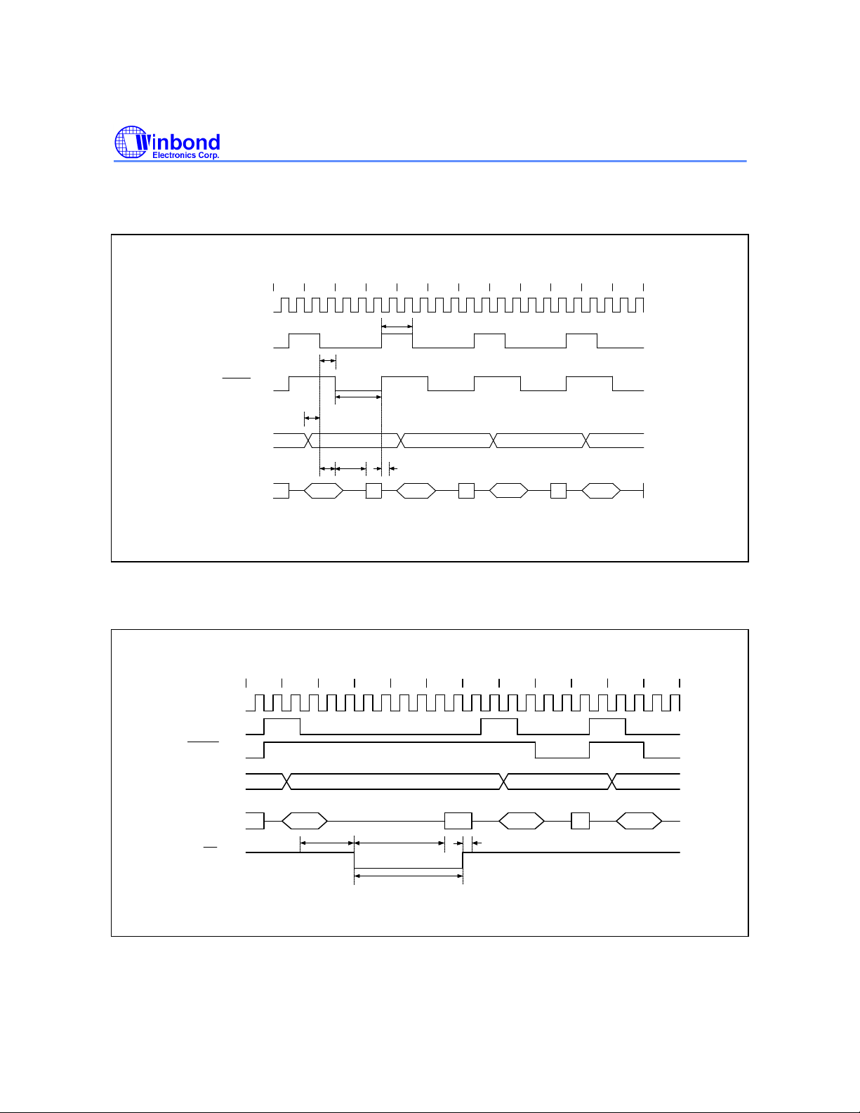
TIMING WAVEFORMS
Program Fetch Cycle
XTAL1
ALE
PSEN
PORT 2
PORT 0
S1
S2 S3 S4 S5 S6 S1 S2 S3 S4 S5 S6
T
ALW
T
APL
T
PSW
T
AAS
T
A0-A7
PDA
T
PDH,TPDZ
A0-A7
DataCode
Code
A0-A7
Data
T
AAH
W78E58
A0-A7
Data Read Cycle
XTAL1
ALE
PSEN
PORT 2
PORT 0
RD
A0-A7
TDAR
A8-A15
TDDA
S2 S3S5 S6 S1S2 S3 S4S5 S6 S1S4
DATA
T
DDH,TDDZ
T
DRD
Publication Release Date: November 1997
- 17 - Revision A2
Page 18
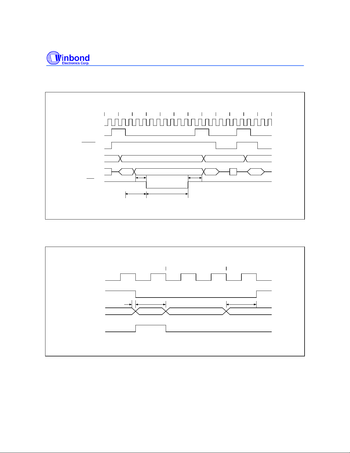
Timing Waveforms, continued
Data Write Cycle
XTAL1
ALE
PSEN
W78E58
S2 S3S5 S6 S1S2 S3 S4S1S5 S6S4
PORT 2
PORT 0
WR
Port Access Cycle
XTAL1
ALE
PORT
T
A8-A15
A0-A7
T
DAW
S5 S6 S1
T
T
PDHPDS
DAD
DATA OUT
T
DWR
T
DWD
T
PDA
DATA OUT
INPUT
SAMPLE
- 18 -
Page 19
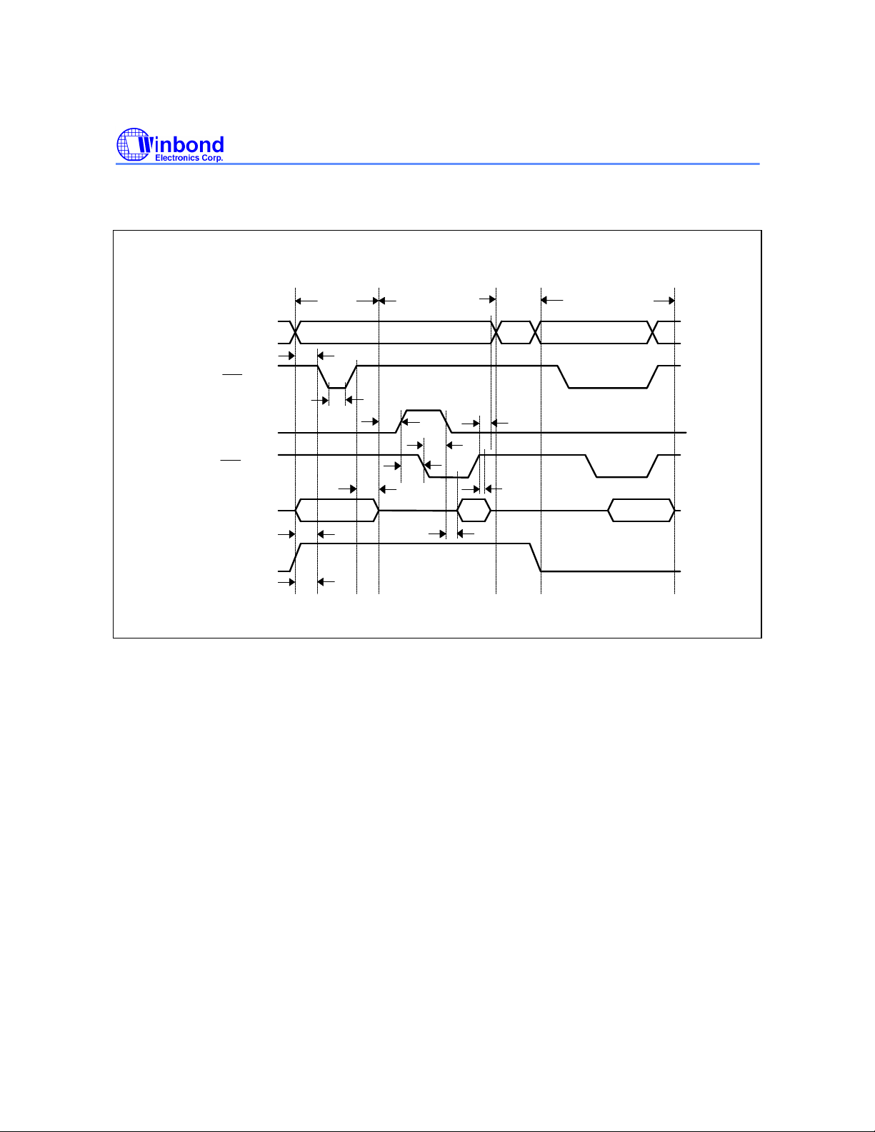
Timing Waveforms, continued
Program Operation
W78E58
P2, P1
(A15... A0)
P3.6
(CE)
P3.3
(OECTRL)
P3.7
(OE)
P0
(A7... A0)
Vpp
V
IH
V
IL
V
IH
V
IL
V
IH
V
IL
V
IH
V
IL
V
IH
V
IL
Vcp
V
IH
Program Program
Verify
Address Stable
T
AS
T
PWP
T
T
OCS
T
OCH
T
OES
T
DH
Data In Data Out
T
DS
T
VPS
AH
T
DFP
D
OUT
T
OEV
Read Verify
Address Valid
Publication Release Date: November 1997
- 19 - Revision A2
Page 20
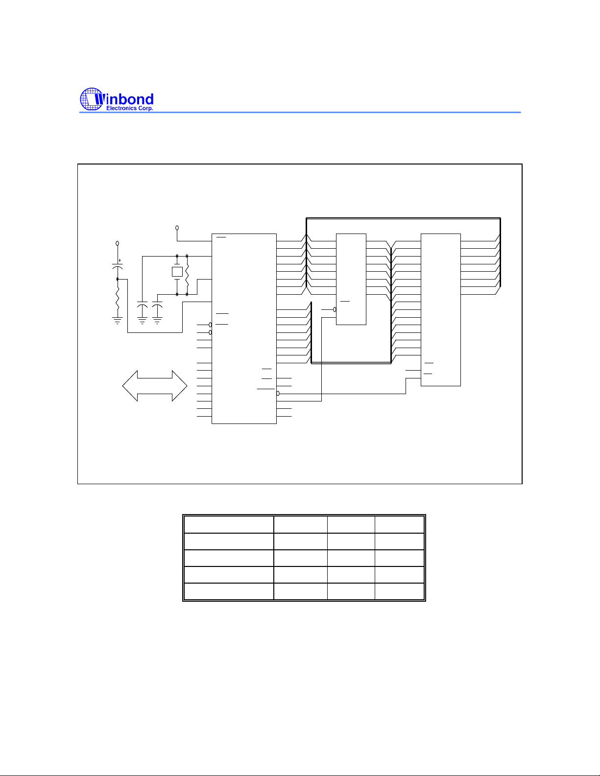
TYPICAL APPLICATION CIRCUITS
Expanded External Program Memory and Crystal
V
CC
V
8.2 K
CC
10 u
C1
CRYSTAL
C2
31
EA
19
XTAL1
R
18
XTAL2
9
RST
INT0
12
13
INT1
14
T0
15
T1
1
P1.0
2
P1.1
3
P1.2
4
P1.3
5
6
7
8
P1.4
P1.5
P1.6
P1.7
W78E58
PSEN
P0.0
P0.1
P0.2
P0.3
P0.4
P0.5
P0.6
P0.7
P2.0
P2.1
P2.2
P2.3
P2.4
P2.5
P2.6
P2.7
RD
WR
ALE
TXD
RXD
38
37
36
35
21
22
23
24
25
26
27
28
39
34
33
32
17
16
29
30
11
10
AD0
AD1
AD2
AD3
AD4
AD5
AD6
AD7
A8
A9
A10
A11
A12
A13
A14
A15
AD0
AD1
AD2
AD3
AD4
AD5
AD6
AD7
GND
3
4
7
8
13
14
17
18
1
11
D0
Q0
D1
Q1
D2
Q2
D3
Q3
D4
Q4
D5
Q5
D6
Q6
D7
Q7
OC
G
74LS373
2
5
6
9
12
15
16
19
A0
A1
A2
A3
A4
A5
A6
A7
A0
A1
A2
A3
A4
A5
A6
A7
A8
A9
A10
A11
A12
A13
A14
A15
GND
10
9
8
7
6
5
4
3
25
24
21
23
2
26
27
1
20
22
A0
A1
A2
A3
A4
A5
A6
A7
A8
A9
A10
A11
A12
A13
A14
A15
CE
OE
27512
W78E58
11
12
13
15
16
17
18
19
AD0
AD1
AD2
AD3
AD4
AD5
AD6
AD7
O0
O1
O2
O3
O4
O5
O6
O7
CRYSTAL C1 C2 R
16 MHz 30P 30P 24 MHz 15P 15P 33 MHz 10P 10P 6.8K
40 MHz 5P 5P 4.7K
Above table shows the reference values for crystal applications.
Note: C1, C2, R components refer to Figure A.
Figure A
- 20 -
Page 21
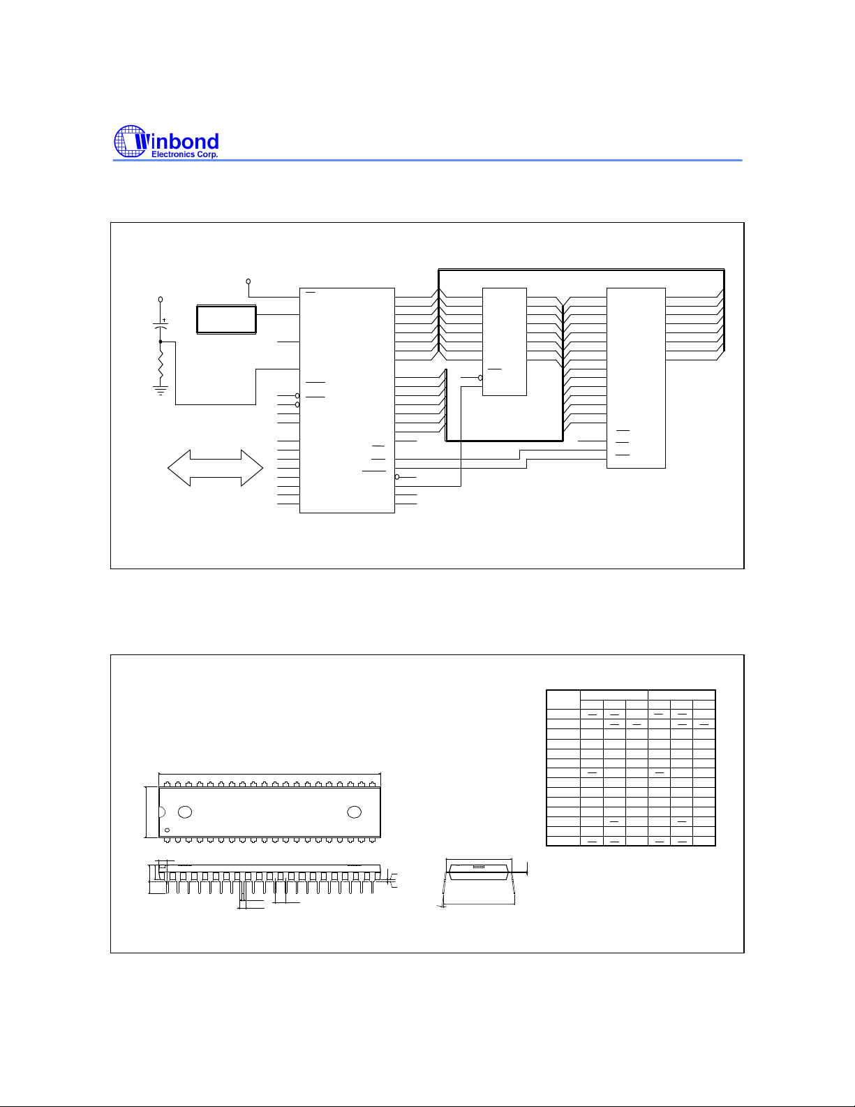
Typical Application Circuits, continued
V
Expanded External Data Memory and Oscillator
CC
V
8.2 K
CC
OSCILLATOR
10 u
19
18
9
12
13
14
15
31
1
2
3
4
5
6
7
8
EA
XTAL1
XTAL2
RST
INT0
INT1
T0
T1
P1.0
P1.1
P1.2
P1.3
P1.4
P1.5
P1.6
P1.7
W78E58
P0.0
P0.1
P0.2
P0.3
P0.4
P0.5
P0.6
P0.7
P2.0 21
P2.1
P2.2
P2.3
P2.4
P2.5
P2.6
P2.7
RD
WR
PSEN
ALE
TXD
RXD
39
AD0
AD1
38
37
AD2
36
AD3
AD4
35
AD5
34
33
AD6
32
AD7
A8
A9
22
23
A10
24
A11
25
A12
26
A13
27
A14
28
17
16
29
30
11
10
AD0
AD1
AD2
AD3
AD4
AD5
AD6
AD7
GND
18
3
4
7
8
13
14
17
11
1
D0
D1
D2
D3
D4
D5
D6
D7
OC
G
74LS373
Q0
Q1
Q2
Q3
Q4
Q5
Q6
Q7
W78E58
A0
A1
A2
A3
A4
A5
A6
A7
A8
A9
A10
A11
A12
A13
A14
GND
10
A0
A1
A2
A3
A4
A5
A6
A7
A8
A9
A10
A11
A12
A13
A14
CE
OE
WR
D0
D1
D2
D3
D4
D5
D6
D7
9
8
7
6
5
4
3
25
24
21
23
2
26
1
20
22
27
A0
2
A1
5
A2
6
A3
9
A4
12
A5
15
A6
16
A7
19
20256
AD0
11
AD1
12
AD2
13
AD3
15
AD4
16
AD5
17
AD6
18
AD7
19
PACKAGE DIMENSIONS
40-pin DIP
40
1
E
1
S
2
A
A
L
D
B
1
B
Figure B
Dimension in inches Dimension in mm
Symbol
A
A
A
B
B 1
c
21
20
1
Base Plane
A
1e
Seating Plane
E
A
e
a
D
E
E
e
L
a
e
S
Notes:
1. Dimension D Max. & S include mold flash or
tie bar burrs.
c
2. Dimension E1 does not include interlead flash.
3. Dimension D & E1 include mold mismatch and
are determined at the mold parting line.
4. Dimension B1 does not include dambar
protrusion/intrusion.
5. Controlling dimension: Inches.
6. General appearance spec. should be based on
final visual inspection spec.
1
2
1
1
A
Min.
0.010
0.150
0.016
0.008
0.540
0.120
0 15
Nom.
Max. Max.
Min.
0.210 5.334
0.160
0.022
0.0540.048
0.014
0.610
0.5500.545
0.110
0.140
0.670
.
0.090
0.254
3.81
0.406
0.203
14.986
13.72
2.286 2.54 2.7940.090 0.100
3.048
0.155
0.018
0.050 1.27
0.010
2.055 2.070
0.6000.590
0.130
0.6500.630 16.00 16.51
Nom.
3.937
0.457
0.254
52.20 52.58
15.24
15.494
13.84
3.302
4.064
0.559
1.3721.219
0.356
13.97
3.556
17.01
150
2.286
Publication Release Date: November 1997
- 21 - Revision A2
Page 22
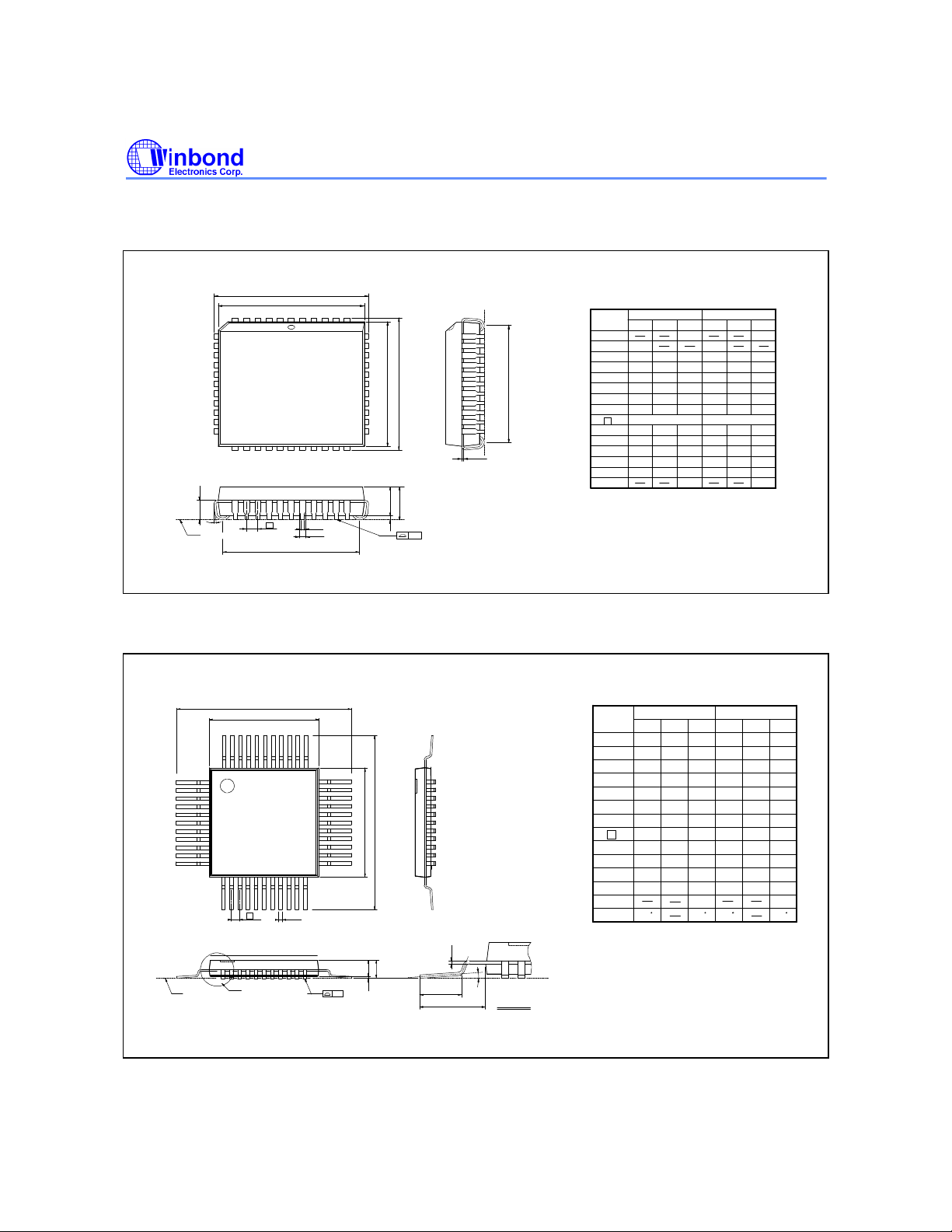
Package Dimensions, continued
1
44-pin PLCC
6 1
7
17
L
θ
Seating Plane
e
H
D
D
44 40
G
D
W78E58
Dimension in inches Dimension in mm
Symbol
39
H
E
E
29
2818
2A
A
b
b
1
A
y
G
E
c
A
A
A
b
b
c
D
E
e
G D
G
H D
H
L
y
Notes:
1. Dimension D & E do not include interlead
flash.
2. Dimension b1 does not include dambar
protrusion/intrusion.
3. Controlling dimension: Inches
4. General appearance spec. should be based
on final visual inspection spec.
Nom.
Min.
0.020
1
0.145
2
0.026
1
0.016
0.008
0.648
0.648
0.590
0.590
E
0.680
0.680
E
0.090
Max. Max.
0.185
0.150
0.155
0.028
0.032
0.022
0.018
0.010
0.014
0.653
0.658
0.653
0.658
0.050 BSC
0.610
0.630
0.6300.610
0.700
0.690
0.7000.690
0.100
0.110
0.004
0.508
3.683
0.406
0.203
16.46
14.99
17.27
17.27
2.296
Min.
0.66
Nom.
4.699
3.81
3.937
0.813
0.711
0.559
0.457
0.254
0.356
16.59
16.71
16.7116.5916.46
1.27
BSC
15.49
16.00
16.0015.4914.99
17.53
17.78
17.7817.53
2.54
2.794
0.10
44-pin QFP
1
11
Seating Plane
H
D
D
44
12
e
34
33
E
EH
22
b
Notes:
c
A
A
See Detail F
2
1
A
y
θ
L
L 1
Detail F
Dimension in inch
Symbol
A
1
A
2
A
b
c
D
E
e
HD
E
H
L
1
L
y
θ
1. Dimension D & E do not include interlead
flash.
2. Dimension b does not include dambar
protrusion/intrusion.
3. Controlling dimension: Millimeter
4. General appearance spec. should be based
on final visual inspection spec.
Nom.
Min.
--- ---
0.002
0.01 0.02 0.25
0.081
0.075
0.01
0.014
0.006 0.152
0.394
0.390
0.390
0.025
0.031
0.510 13.45
0.520
0.520
0.510
0.025
0.031
0.063
0.051 0.075 1.295
0
Dimension in mm
Max. Max.
---
0.087
0.018
0.0100.004
0.398
0.3980.394
0.036
0.530
0.530
0.037
0.003
Nom.
Min.
--- ---
0.05
1.90
0.25
2.05
0.35
0.5
2.20
0.45
0.2540.101
10.00
9.9
9.9
0.635
12.95
12.95
0.65
10.00
0.80
13.2
10.1
10.1
0.952
13.4513.2
0.8
0.95
1.6
1.905
0.08
7
0
---
7
- 22 -
Page 23
Timing Waveforms, continued
1
2
Headquarters
No. 4, Creation Rd. III,
Science-Based Industrial Park,
Hsinchu, Taiwan
TEL: 886-3-5770066
FAX: 886-3-5792697
http://www.winbond.com.tw/
Voice & Fax-on-demand: 886-2-27197006
Taipei Office
11F, No. 115, Sec. 3, Min-Sheng East Rd.,
Taipei, Taiwan
TEL: 886-2-27190505
FAX: 886-2-27197502
Winbond Electronics (H.K.) Ltd.
Rm. 803, World Trade Square, Tower II,
123 Hoi Bun Rd., Kwun Tong,
Kowloon, Hong Kong
TEL: 852-27513100
FAX: 852-27552064
Winbond Electronics North America Corp.
Winbond Memory Lab.
Winbond Microelectronics Corp.
Winbond Systems Lab.
2727 N. First Street, San Jose,
CA 95134, U.S.A.
TEL: 408-9436666
FAX: 408-5441798
Note: All data and specifications are subject to change without notice.
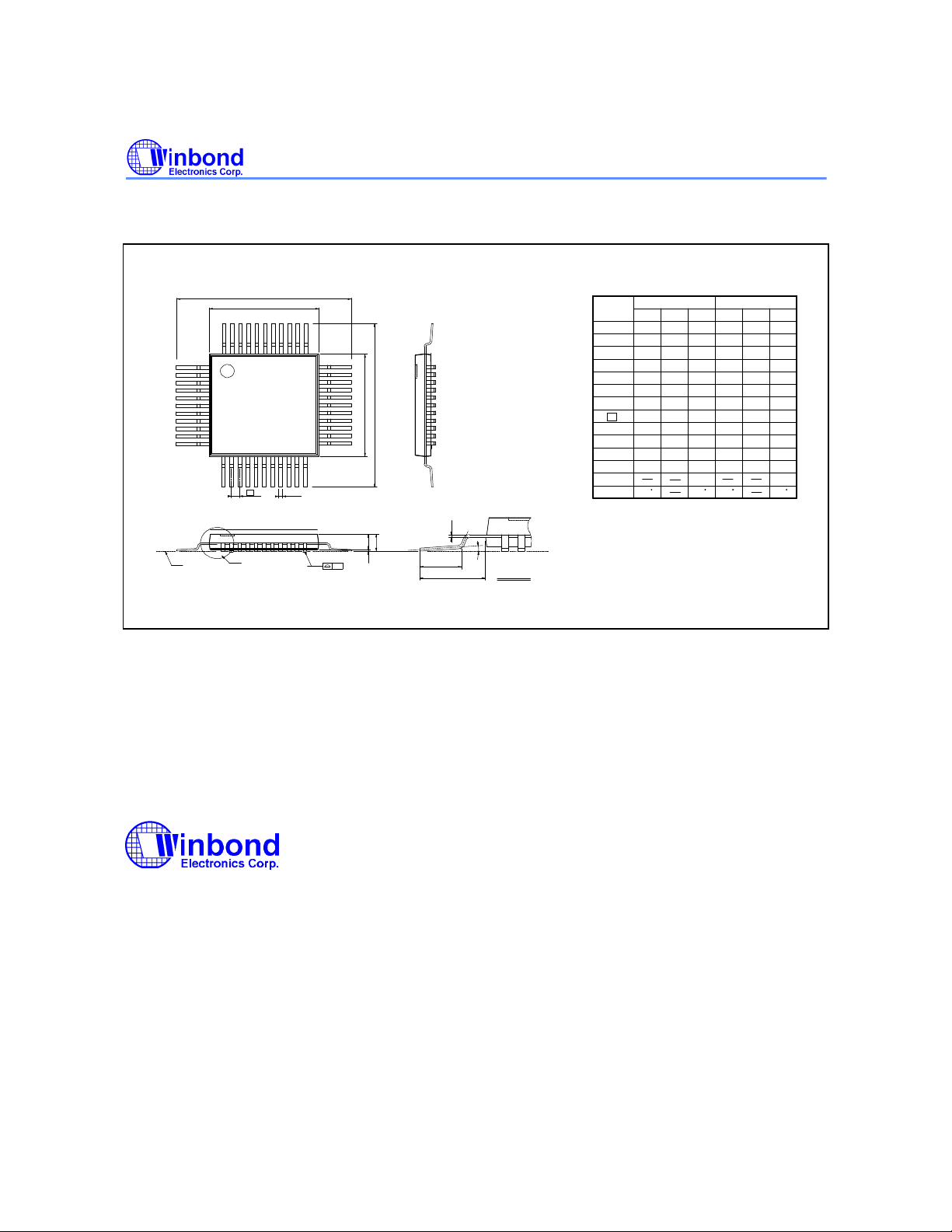
44-pin TQFP
H
D
44
1
11
12
Seating Plane
D
e
See Detail F
W78E58
Dimension in inch Dimension in mm
Symbol
34
33
E
EH
22
b
Notes:
c
A
A
A
1
y
θ
L
L
Detail F
Min. Nom. Max. Max.Nom.Min.
A
1
A
2
A
b
c
D
E
e
D
H
E
H
L
1
L
y
θ
1. Dimension D & E do not include interlead
flash.
2. Dimension b does not include dambar
protrusion/intrusion.
3. Controlling dimension: Millimeter
4. General appearance spec. should be based
on final visual inspection spec.
--- ---
0.002
0.004
0.037
0.039
0.0039
0.013
---
0.394
0.390
0.390
0.025
0.031
0.468 12.10
0.472
0.472
0.468
0.018
0.024
0.039
---
0
0.047
0.006
0.041
0.015
0.0080.004
0.398
0.3980.394
0.036
0.476
0.476
0.030
0.003
---
7
--- ---
0.05
0.95
0.22
9.9
9.9
0.635
11.90
11.90
0.45
--- ---
0
0.10
1.00
0.32
10.00
10.00
12.00
1.20
0.15
1.05
0.38
0.2000.090
---
10.1
10.1
0.952
0.80
12.1012.00
0.60
0.75
1.00
0.08
7
Publication Release Date: November 1997
- 23 - Revision A2
 Loading...