

Page 1

查询W78E054C供应商
W78E54C/W78E054C Data Sheet
8-BIT MICROCONTROLLER
Table of Contents-
1. GENERAL DESCRIPTION......................................................................................................... 3
2. FEATURES................................................................................................................................. 3
3. PIN CONFIGURATIONS ............................................................................................................ 4
4. PIN DESCRIPTION..................................................................................................................... 5
5. FUNCTIONAL DESCRIPTION ................................................................................................... 6
5.1 Timers 0, 1, and 2........................................................................................................... 6
5.2 New Defined Peripheral.................................................................................................. 6
5.2.1
5.2.2 PORT4 .............................................................................................................................7
5.2.3 Reduce EMI Emission......................................................................................................7
5.3 Power-off Flag ................................................................................................................ 8
5.4 Watchdog Timer ............................................................................................................. 8
5.5 Clock............................................................................................................................. 10
5.6 Power Management...................................................................................................... 10
5.7 Reset............................................................................................................................. 10
6. SECURITY BITS....................................................................................................................... 11
6.1 Lock Bit.........................................................................................................................11
6.2 MOVC Inhibit................................................................................................................. 12
6.3 Encryption..................................................................................................................... 12
7. ELECTRICAL CHARACTERISTICS......................................................................................... 13
7.1 Absolute Maximum Ratings.......................................................................................... 13
7.2 D.C. Characteristics......................................................................................................13
7.3 A.C. Characteristics...................................................................................................... 15
7.3.1 Clock Input Waveform....................................................................................................15
7.3.2 Program Fetch Cycle......................................................................................................15
7.3.3 Data Read Cycle ............................................................................................................16
7.3.4 Data Write Cycle.............................................................................................................16
7.3.5 Port Access Cycle ..........................................................................................................16
7.3.6 Program Operation.........................................................................................................17
INT2
/ NT3I ....................................................................................................................6
8. TIMING WAVEFORMS............................................................................................................. 18
Publication Release Date: October 3, 2006
- 1 - Revision A4
Page 2

W78E54C/W78E054C
8.1 Program Fetch Cycle.................................................................................................... 18
8.2 Data Read Cycle........................................................................................................... 18
8.3 Data Write Cycle........................................................................................................... 19
8.4 Port Access Cycle......................................................................................................... 19
9. TYPICAL APPLICATION CIRCUITS........................................................................................20
9.1 Expanded External Program Memory and Crystal....................................................... 20
9.2 Expanded External Data Memory and Oscillator ......................................................... 21
10. PACKAGE DIMENSIONS......................................................................................................... 22
10.1 40-pin DIP..................................................................................................................... 22
10.2 44-pin PLCC ................................................................................................................. 22
10.3 44-pin PQFP................................................................................................................. 23
11. REVISION HISTORY................................................................................................................ 24
- 2 -
Page 3

W78E54C/W78E054C
1. GENERAL DESCRIPTION
The W78E054C is an 8-bit microcontroller which can accommodate a wider frequency range with low
power consumption. The instruction set for the W78E054C is fully compatible with the standard 8051.
The W78E054C contains an 16K bytes Flash EPROM; a 256 bytes RAM; four 8-bit bi-directional and
bit-addressable I/O ports; an additional 4-bit I/O port P4; three 16-bit timer/counters; a hardware
watchdog timer and a serial port. These peripherals are supported by eight sources two-level interrupt
capability. To facilitate programming and verification, the Flash EPROM inside the W78E054C allows
the program memory to be programmed and read electronically. Once the code is confirmed, the user
can protect the code for security.
The W78E054C microcontroller has two power reduction modes, idle mode and power-down mode,
both of which are software selectable. The idle mode turns off the processor clock but allows for
continued peripheral operation. The power-down mode stops the crystal oscillator for minimum power
consumption. The external clock can be stopped at any time and in any state without affecting the
processor.
2. FEATURES
• Fully static design 8-bit CMOS microcontroller
• Wide supply voltage of 4.5V to 5.5V
• 256 bytes of on-chip scratchpad RAM
• 16 KB electrically erasable/programmable Flash EPROM
• 64 KB program memory address space
• 64 KB data memory address space
• Four 8-bit bi-directional ports
• One extra 4-bit bit-addressable I/O port, additional
(available on 44-pin PLCC/QFP package)
• Three 16-bit timer/counters
• One full duplex serial port(UART)
• Watchdog Timer
• Eight sources, two-level interrupt capability
• EMI reduction mode
• Built-in power management
• Code protection mechanism
• Packages:
− Lead Free (RoHS) DIP 40: W78E054C40DL
− Lead Free (RoHS) PLCC 44: W78E054C40PL
− Lead Free (RoHS) PQFP 44: W78E054C40FL
INT2
/ INT3
Publication Release Date: October 3, 2006
- 3 - Revision A4
Page 4
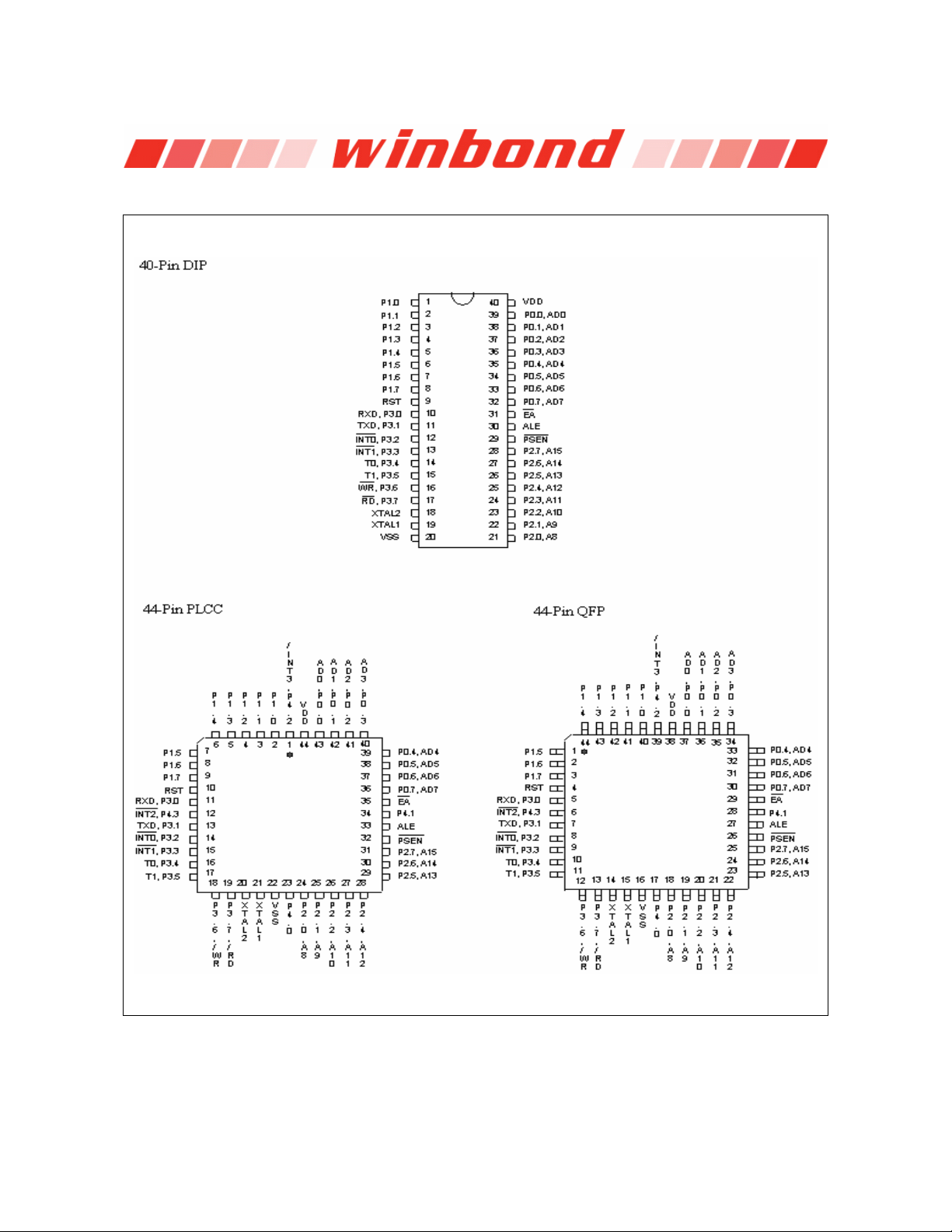
3. PIN CONFIGURATIONS
W78E54C/W78E054C
- 4 -
Page 5
W78E54C/W78E054C
A
A
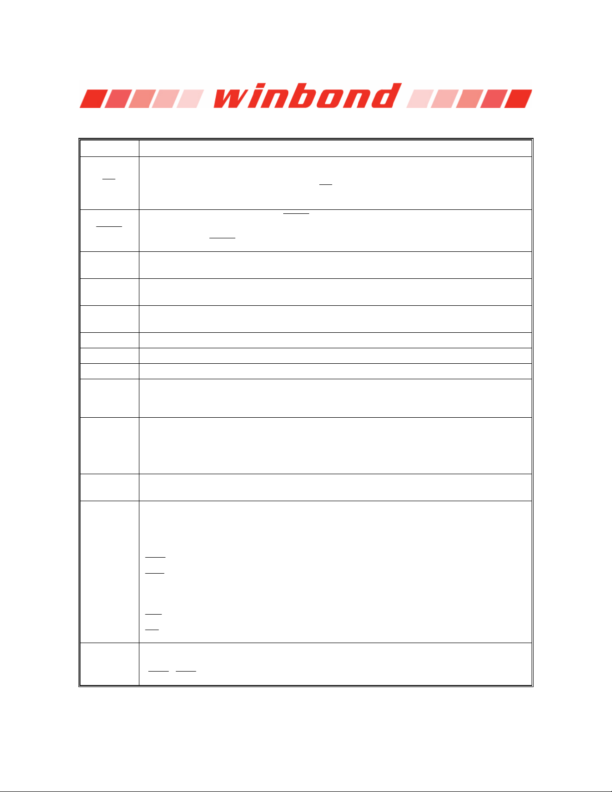
4. PIN DESCRIPTION
SYMBOL DESCRIPTIONS
EXTERNAL ACCESS ENABLE: This pin forces the processor to execute out of
E
PSEN
ALE
RST
XTAL1
XTAL2
VSS
VDD
P0.0−P0.7
P1.0−P1.7
P2.0−P2.7
P3.0−P3.7
P4.0−P4.3
external ROM. It should be kept high to access internal ROM. The ROM address and
data will not be presented on the bus if
within on-chip ROM area.
PROGRAM STORE ENABLE:
address/ data bus during fetch and MOVC operations. When internal ROM access is
performed, no
ADDRESS LATCH ENABLE: ALE is used to enable the address latch that separates
the address from the data on Port 0.
RESET: A high on this pin for two machine cycles while the oscillator is running resets
the device.
CRYSTAL1: This is the crystal oscillator input. This pin may be driven by an external
clock.
CRYSTAL2: This is the crystal oscillator output. It is the inversion of XTAL1.
GROUND: Ground potential
POWER SUPPLY: Supply voltage for operation.
PORT 0: Port 0 is a bi-directional I/O port which also provides a multiplexed low order
address/data bus during accesses to external memory. The Port 0 is also an opendrain port and external pull-ups need to be connected while in programming.
PORT 1: Port 1 is a bi-directional I/O port with internal pull-ups. The bits have alternate
functions which are described below:
T2(P1.0): Timer/Counter 2 external count input
T2EX(P1.1): Timer/Counter 2 Reload/Capture control
PORT 2: Port 2 is a bi-directional I/O port with internal pull-ups. This port also provides
the upper address bits for accesses to external memory.
PORT 3: Port 3 is a bi-directional I/O port with internal pull-ups. All bits have alternate
functions, which are described below:
RXD(P3.0) : Serial Port receiver input
TXD(P3.1) : Serial Port transmitter output
INT0 (P3.2) : External Interrupt 0
INT1
(P3.3) : External Interrupt 1
T0(P3.4) : Timer 0 External Input
T1(P3.5) : Timer 1 External Input
WR
(P3.6) :External Data Memory Write Strobe
RD
(P3.7) : External Data Memory Read Strobe
PORT 4: Another bit-addressable bidirectional I/O port P4. P4.3 and P4.2 are alternative
function pins. It can be used as general I/O port or external interrupt input sources
INT2
/INT3 ).
(
PSEN strobe signal outputs from this pin.
PSEN enables the external ROM data onto the Port 0
E
pin is high and the program counter is
Publication Release Date: October 3, 2006
- 5 - Revision A4
Page 6

W78E54C/W78E054C
5. FUNCTIONAL DESCRIPTION
The W78E054C architecture consists of a core controller surrounded by various registers, five general
purpose I/O ports, 256 bytes of RAM, three timer/counters, and a serial port. The processor supports
111 different opcodes and references both a 64K program address space and a 64K data storage
space.
5.1 Timers 0, 1, and 2
Timers 0, 1, and 2 each consist of two 8-bit data registers. These are called TL0 and TH0 for Timer 0,
TL1 and TH1 for Timer 1, and TL2 and TH2 for Timer 2. The TCON and TMOD registers provide
control functions for timers 0 and 1. The T2CON register provides control functions for Timer 2.
RCAP2H and RCAP2L are used as reload/capture registers for Timer 2.
The operations of Timer 0 and Timer 1 are the same as in the W78C51. Timer 2 is a special feature of
the W78E054C: it is a 16-bit timer/counter that is configured and controlled by the T2CON register.
Like Timers 0 and 1, Timer 2 can operate as either an external event counter or as an internal timer,
depending on the setting of bit C/T2 in T2CON. Timer 2 has three operating modes: capture, autoreload, and baud rate generator. The clock speed at capture or auto-reload mode is the same as that
of Timers 0 and 1.
5.2 New Defined Peripheral
In order to be more suitable for I/O, an extra 4-bit bit-addressable port P4 and two external interrupt
INT2
, INT3 has been added to either the PLCC or QFP 44-pin package. And description follows:
5.2.1
Two additional external interrupts,
interrupt 0 and 1 in the standard 80C52. The functions/status of these interrupts are
determined/shown by the bits in the XICON (External Interrupt Control) register. The XICON register is
bit-addressable but is not a standard register in the standard 80C52. Its address is at 0C0H. To
set/clear bits in the XICON register, one can use the "SETB (/CLR) bit" instruction. For example,
"SETB 0C2H" sets the EX2 bit of XICON.
XICON - external interrupt control (C0H)
PX3 EX3 IE3 IT3 PX2 EX2 IE2 IT2
PX3: External interrupt 3 priority high if set
EX3: External interrupt 3 enable if set
IE3: If IT3 = 1, IE3 is set/cleared automatically by hardware when interrupt is detected/serviced
IT3: External interrupt 3 is falling-edge/low-level triggered when this bit is set/cleared by software
PX2: External interrupt 2 priority high if set
EX2: External interrupt 2 enable if set
IE2: If IT2 = 1, IE2 is set/cleared automatically by hardware when interrupt is detected/serviced
IT2: External interrupt 2 is falling-edge/low-level triggered when this bit is set/cleared by software
INT2
/ NT3I
INT2
and INT3, whose functions are similar to those of external
- 6 -
Page 7
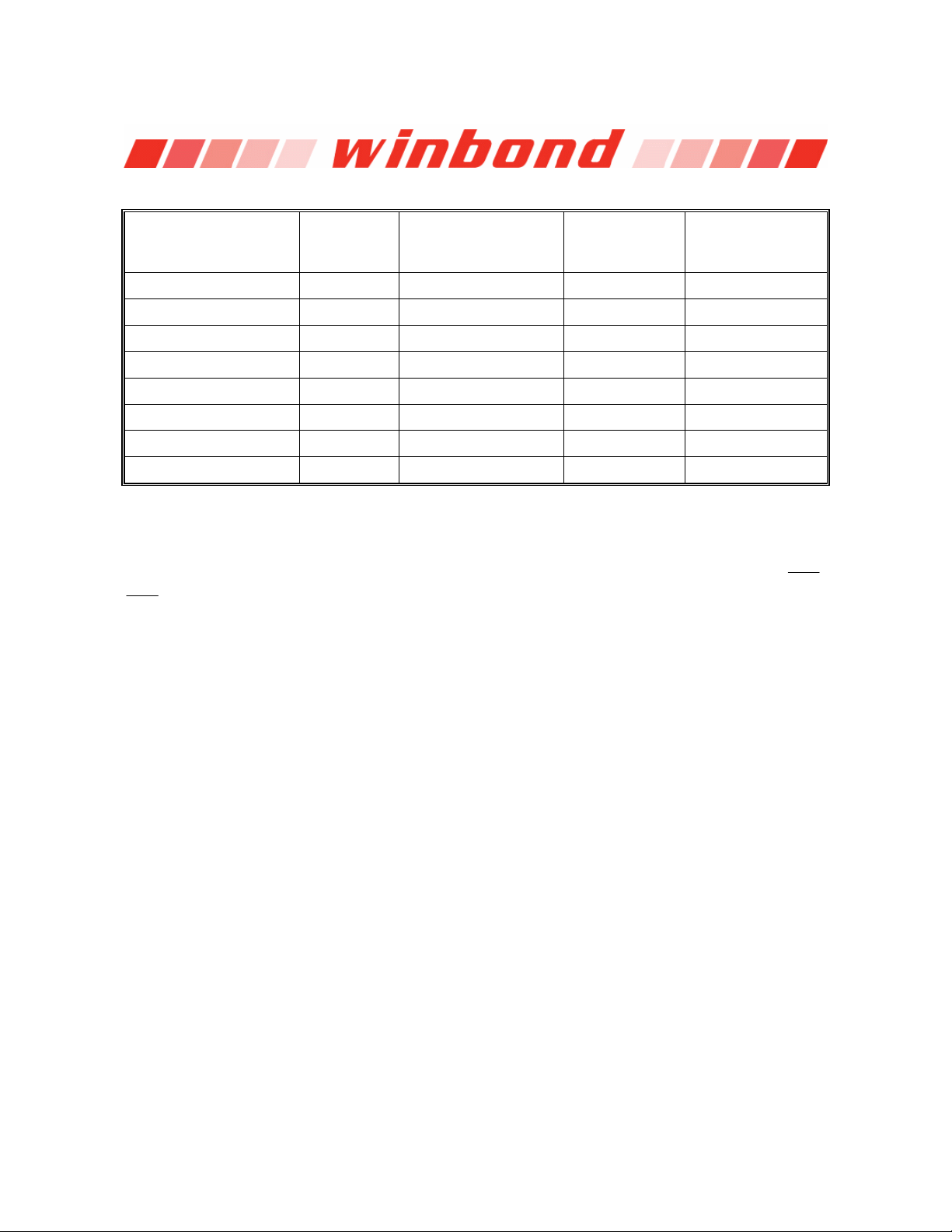
Eight-source interrupt information
W78E54C/W78E054C
INTERRUPT SOURCE
External Interrupt 0 03H 0 (highest) IE.0 TCON.0
Timer/Counter 0 0BH 1 IE.1 External Interrupt 1 13H 2 IE.2 TCON.2
Timer/Counter 1 1BH 3 IE.3 Serial Port 23H 4 IE.4 Timer/Counter 2 2BH 5 IE.5 External Interrupt 2 33H 6 XICON.2 XICON.0
External Interrupt 3 3BH 7 (lowest) XICON.6 XICON.3
VECTOR
ADDRESS
POLLING
SEQUENCE WITHIN
PRIORITY LEVEL
ENABLE
REQUIRED
SETTINGS
INTERRUPT
TYPE
EDGE/LEVEL
5.2.2 PORT4
Another bit-addressable port P4 is also available and only 4 bits (P4<3:0>) can be used. This port
address is located at 0D8H with the same function as that of port P1, except the P4.3 and P4.2 are
alternative function pins. It can be used as general I/O pins or external interrupt input sources (
INT3 ).
Example:
P4 REG 0D8H
MOV P4, #0AH ; Output data "A" through P4.0−P4.3.
MOV A, P4 ; Read P4 status to Accumulator.
SETB P4.0 ; Set bit P4.0
CLR P4.1 ; Clear bit P4.1
INT2
,
5.2.3 Reduce EMI Emission
Because of on-chip Flash EPROM, when a program is running in internal ROM space, the ALE will be
unused. The transition of ALE will cause noise, so it can be turned off to reduce the EMI emission if it
is useless. Turning off the ALE signal transition only requires setting the bit 0 of the AUXR SFR, which
is located at 08Eh. When ALE is turned off, it will be reactivated when the program accesses external
ROM/RAM data or jumps to execute an external ROM code. The ALE signal will turn off again after it
has been completely accessed or the program returns to internal ROM code space. The AO bit in the
AUXR register, when set, disables the ALE output. In order to reduce EMI emission from oscillation
circuitry, W78E054C allows user to diminish the gain of on-chip oscillator amplifiers by using
programmer to clear the B7 bit of security register. Once B7 is set to 0, a half of gain will be
decreased. Care must be taken if user attempts to diminish the gain of oscillator amplifier, reducing a
half of gain may affect the external crystal operating improperly at high frequency above 24 MHz. The
value of R and C1, C2 may need some adjustment while running at lower gain.
Publication Release Date: October 3, 2006
- 7 - Revision A4
Page 8
W78E54C/W78E054C
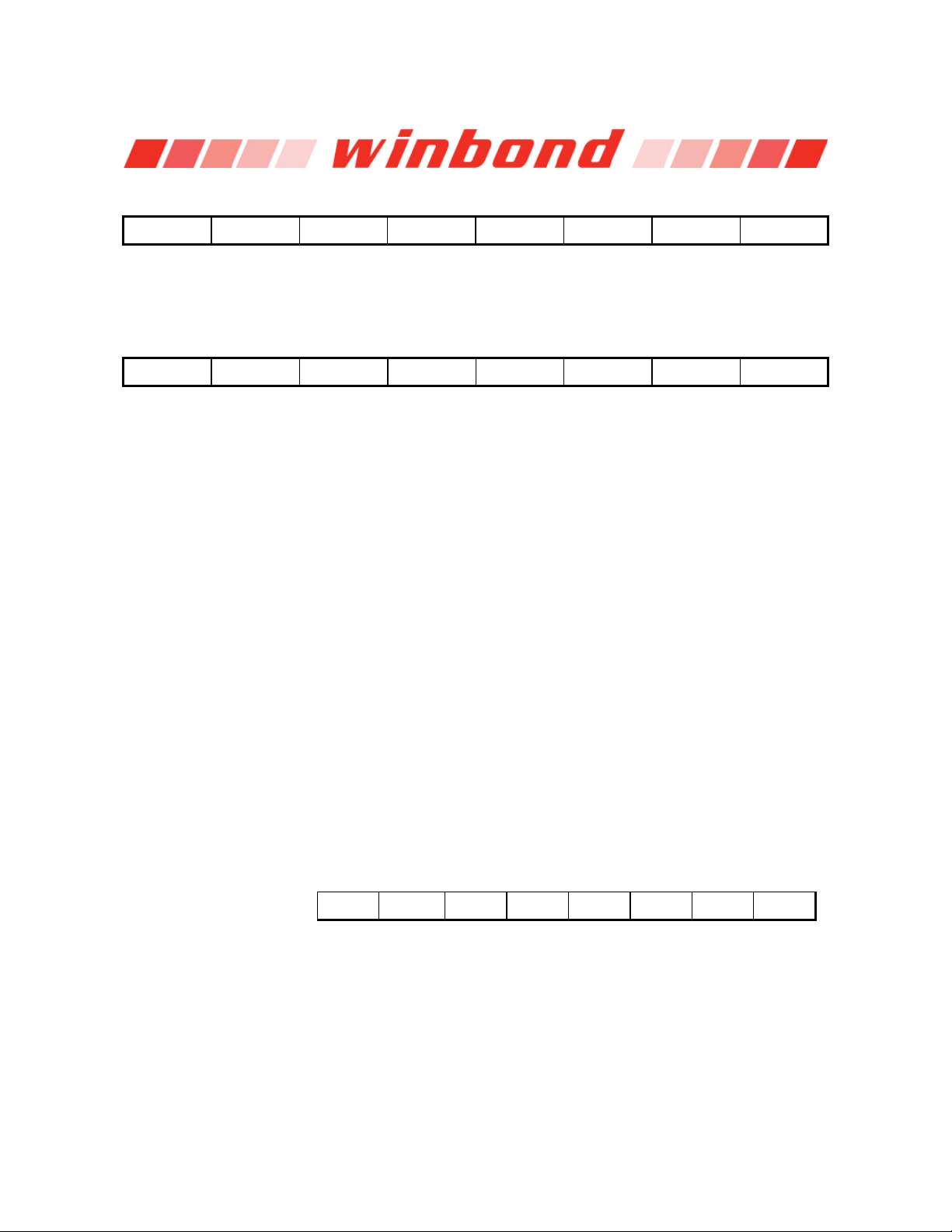
***AUXR - Auxiliary register (8EH)
- - - - - - - AO
AO: Turn off ALE output.
5.3 Power-off Flag
***PCON - Power control (87H)
- - - POF GF1 GF0 PD IDL
POF: Power off flag. Bit is set by hardware when power on reset. It can be cleared by software
to determine chip reset is a warm boot or cold boot.
GF1, GF0: These two bits are general-purpose flag bits for the user.
PD: Power down mode bit. Set it to enter power down mode.
IDL: Idle mode bit. Set it to enter idle mode.
The power-off flag is located at PCON.4. This bit is set when V
be used to determine if a reset is a warm boot or a cold boot if it is subsequently reset by software.
DD has been applied to the part. It can
5.4 Watchdog Timer
The Watchdog timer is a free-running timer which can be programmed by the user to serve as a
system monitor, a time-base generator or an event timer. It is basically a set of dividers that divide the
system clock. The divider output is selectable and determines the time-out interval. When the time-out
occurs, a system reset can also be caused if it is enabled. The main use of the Watchdog timer is as a
system monitor. This is important in real-time control applications. In case of power glitches or electromagnetic interference, the processor may begin to execute errant code. If this is left unchecked the
entire system may crash. The watchdog time-out selection will result in different time-out values
depending on the clock speed. The Watchdog timer will be disabled on reset. In general, software
should restart the Watchdog timer to put it into a known state. The control bits that support the
Watchdog timer are discussed below.
Watchdog Timer Control Register
Bit: 7 6 5 4 3 2 1 0
ENW CLRW WIDL - - PS2 PS1 PS0
Mnemonic: WDTC Address: 8FH
ENW : Enable watch-dog if set.
CLRW : Clear watch-dog timer and prescaler if set. This flag will be cleared automatically
WIDL : If this bit is set, watch-dog is enabled under IDLE mode. If cleared, watch-dog is disabled
under IDLE mode. Default is cleared.
PS2, PS1, PS0: Watch-dog prescaler timer select. Prescaler is selected when set PS2~0 as follows:
- 8 -
Page 9
W78E54C/W78E054C
PS2 PS1 PS0 PRESCALER SELECT
0 0 0 2
0 0 1 4
0 1 0 8
0 1 1 16
1 0 0 32
1 0 1 64
1 1 0 128
1 1 1 256
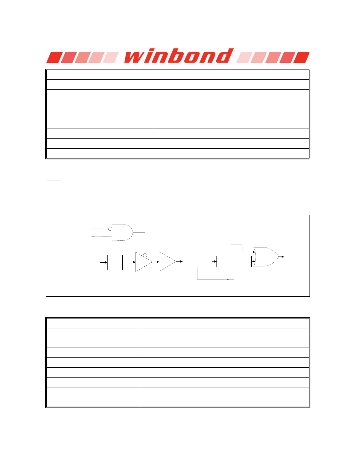
The time-out period is obtained using the following equation:
1
14
2 PRESCALER 1000 12 mS
×× × ×
OSC
Before Watchdog time-out occurs, the program must clear the 14-bit timer by writing 1 to WDTC.6
(CLRW). After 1 is written to this bit, the 14-bit timer, prescaler and this bit will be reset on the next
instruction cycle. The Watchdog timer is cleared on reset.
WIDL
IDLE
OSC 1/12
ENW
PRESCALER
Watchdog Timer Block Diagram
Typical Watch-Dog time-out period when OSC = 20 MHz
PS2 PS1 PS0 WATCHDOG TIME-OUT PERIOD
0 0 0 19.66 mS
0 0 1 39.32 mS
0 1 0 78.64 mS
0 1 1 157.28 mS
1 0 0 314.57 mS
1 0 1 629.14 mS
1 1 0 1.25 S
1 1 1 2.50 S
CLRW
EXTERNAL
RESET
14-BIT TIMER
CLEAR
INTERNAL
RESET
Publication Release Date: October 3, 2006
- 9 - Revision A4
Page 10

W78E54C/W78E054C
5.5 Clock
The W78E054C is designed to be used with either a crystal oscillator or an external clock. Internally,
the clock is divided by two before it is used. This makes the W78E054C relatively insensitive to duty
cycle variations in the clock. The W78E054C incorporates a built-in crystal oscillator. To make the
oscillator work, a crystal must be connected across pins XTAL1 and XTAL2. In addition, a load
capacitor must be connected from each pin to ground. An external clock source should be connected
to pin XTAL1. Pin XTAL2 should be left unconnected. The XTAL1 input is a CMOS-type input, as
required by the crystal oscillator.
5.6 Power Management
Idle Mode
The idle mode is entered by setting the IDL bit in the PCON register. In the idle mode, the internal
clock to the processor is stopped. The peripherals and the interrupt logic continue to be clocked. The
processor will exit idle mode when either an interrupt or a reset occurs.
Power-down Mode
When the PD bit of the PCON register is set, the processor enters the power-down mode. In this
mode all of the clocks are stopped, including the oscillator. The only way to exit power-down mode is
by a reset.
5.7 Reset
The external RESET signal is sampled at S5P2. To take effect, it must be held high for at least two
machine cycles while the oscillator is running. An internal trigger circuit in the reset line is used to
deglitch the reset line when the W78E054C is used with an external RC network. The reset logic also
has a special glitch removal circuit that ignores glitches on the reset line.
During reset, the ports are initialized to FFH, the stack pointer to 07H, PCON (with the exception of bit
4) to 00H, and all of the other SFR registers except SBUF to 00H. SBUF is not reset.
- 10 -
Page 11
W78E54C/W78E054C
r
6. SECURITY BITS
During the on-chip Flash EPROM operation mode, the Flash EPROM can be programmed and
verified repeatedly. Until the code inside the Flash EPROM is confirmed OK, the code can be
protected. The protection of Flash EPROM and those operations on it are described below.
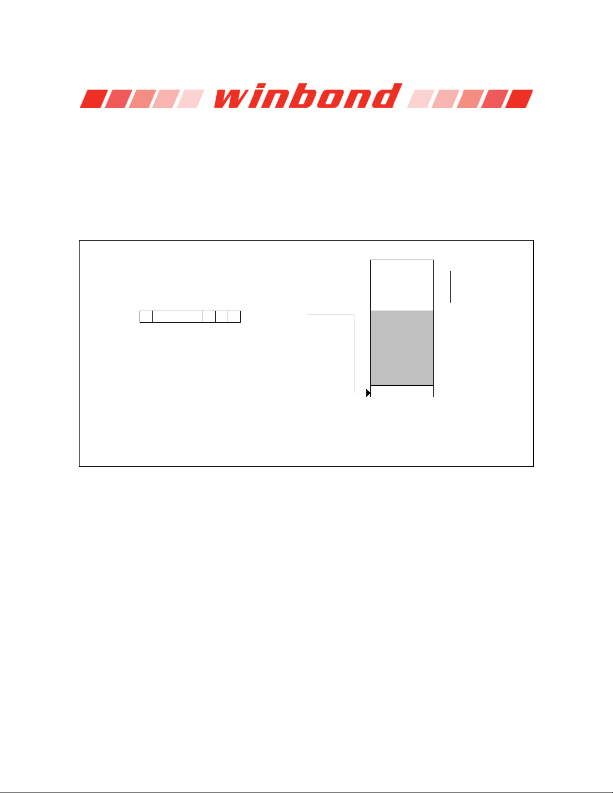
The W78E054C has a Security Register which can not be accessed in normal mode. These registers
can only be accessed from the Flash EPROM operation mode. Those bits of the Security Register can
not be changed once they have been programmed from high to low. They can only be reset through
erase-all operation. The Security Register is addressed in the Flash EPROM operation mode by
address #0FFFFh.
0000h
3FFFh
0FFFFh
B0B1
Reserved
B7
B0 : Lock bit, logic 0 : active
B1 : MOVC inhibit,
logic 0 : the MOVC instruction in external memory
cannot access the code in internal memory.
logic 1 : no restriction.
B2 : Encryption
logic 0 : the encryption logic enable
logic 1 : the encryption logic disable
B7 : Osillator Control
logic 0 : 1/2 gain
logic 1 : Full gain
Default 1 for all security bits.
B2
Security Bits
Reserved bits must be kept in logic 1.
Special Setting Registe
16KB On-chip ROM
Program Memory
Reserved
Security Register
6.1 Lock Bit
This bit is used to protect the customer's program code in the W78E054C. It may be set after the
programmer finishes the programming and verifies sequence. Once this bit is set to logic 0, both the
Flash EPROM data and Special Setting Register can not be accessed again.
Publication Release Date: October 3, 2006
- 11 - Revision A4
Page 12

W78E54C/W78E054C
6.2 MOVC Inhibit
This bit is used to restrict the accessible region of the MOVC instruction. It can prevent the MOVC
instruction in external program memory from reading the internal program code. When this bit is set to
logic 0, a MOVC instruction in external program memory space will be able to access code only in the
external memory, not in the internal memory. A MOVC instruction in internal program memory space
will always be able to access the ROM data in both internal and external memory. If this bit is logic 1,
there are no restrictions on the MOVC instruction.
6.3 Encryption
This bit is used to enable/disable the encryption logic for code protection. Once encryption feature is
enabled, the data presented on port 0 will be encoded via encryption logic. Only whole chip erase will
reset this bit.
- 12 -
Page 13
7. ELECTRICAL CHARACTERISTICS
A
7.1 Absolute Maximum Ratings
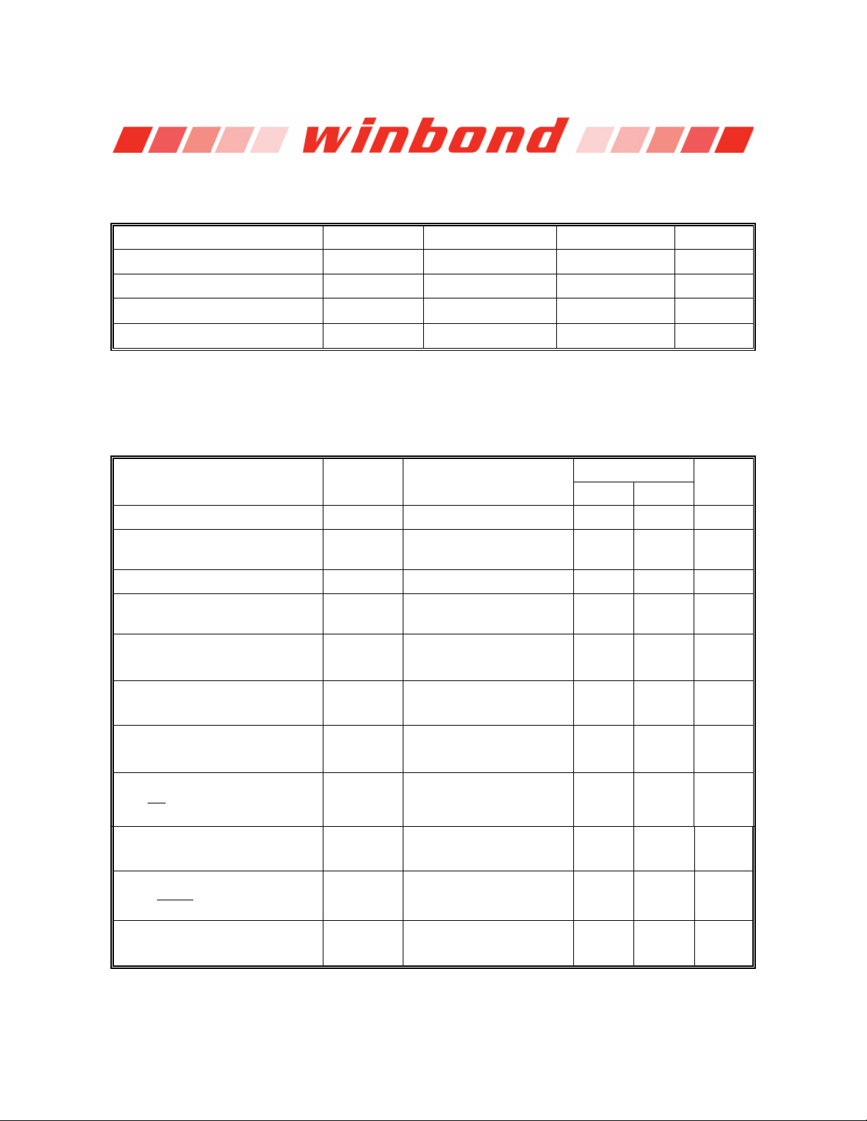
PARAMETER SYMBOL MIN. MAX. UNIT
W78E54C/W78E054C
DC Power Supply
V
DD−VSS
-0.3 +7.0 V
Input Voltage VIN VSS -0.3 VDD +0.3 V
Operating Temperature TA 0 70
Storage Temperature TST -55 +150
Note: Exposure to conditions beyond those listed under Absolute Maximum Ratings may adversely affect the life and reliability
of the device.
°C
°C
7.2 D.C. Characteristics
(VCC−VSS = 5V ±10%, TA = 25° C, unless otherwise specified.)
PARAMETER SYMBOL TEST CONDITIONS
Operating Voltage VDD
Operating Current IDD
No load, V
RST = 1
-
DD = 5.5V,
Idle Current IIDLE Idle mode VDD = 5.5V - 6 mA
Power Down Current IPWDN
Input Current
I
IN1
P1, P2, P3, P4
Logical 1-to-0 Transition
Current P1, P2, P3
(*1)
, P4
Input Current
RST (*2)
TL
I
IIN2
Input Leakage Current
Power-down mode
DD = 5.5V
V
V
DD = 5.5V
= 0V or V
IN
V
V
DD = 5.5V
V
IN = 2.0V
(*1)
DD
VDD = 5.5V
VIN = VDD
VDD = 5.5V
ILK
E
P0,
Output Low Voltage
P1, P2, P3, P4
Output Low Voltage
ALE,
PSEN
, P0
(*3)
Output High Voltage
P1, P2, P3, P4
V
OL1
OL2
V
V
OH1
0V < VIN < VDD
V
DD = 4.5V
= +2 mA
IOL1
V
DD = 4.5V
= +4 mA
I
OL2
V
DD = 4.5V
OH1 = -100 μA
I
PECIFICATION
MIN. MAX.
UNIT
4.5 5.5 V
- 20 mA
- 50
-50 +10
-550 -
-10 +300
-10 +10
μA
μA
μA
μA
μA
- 0.45 V
- 0.45 V
2.4 - V
Publication Release Date: October 3, 2006
- 13 - Revision A4
Page 14
DC Characteristics, continued
W78E54C/W78E054C
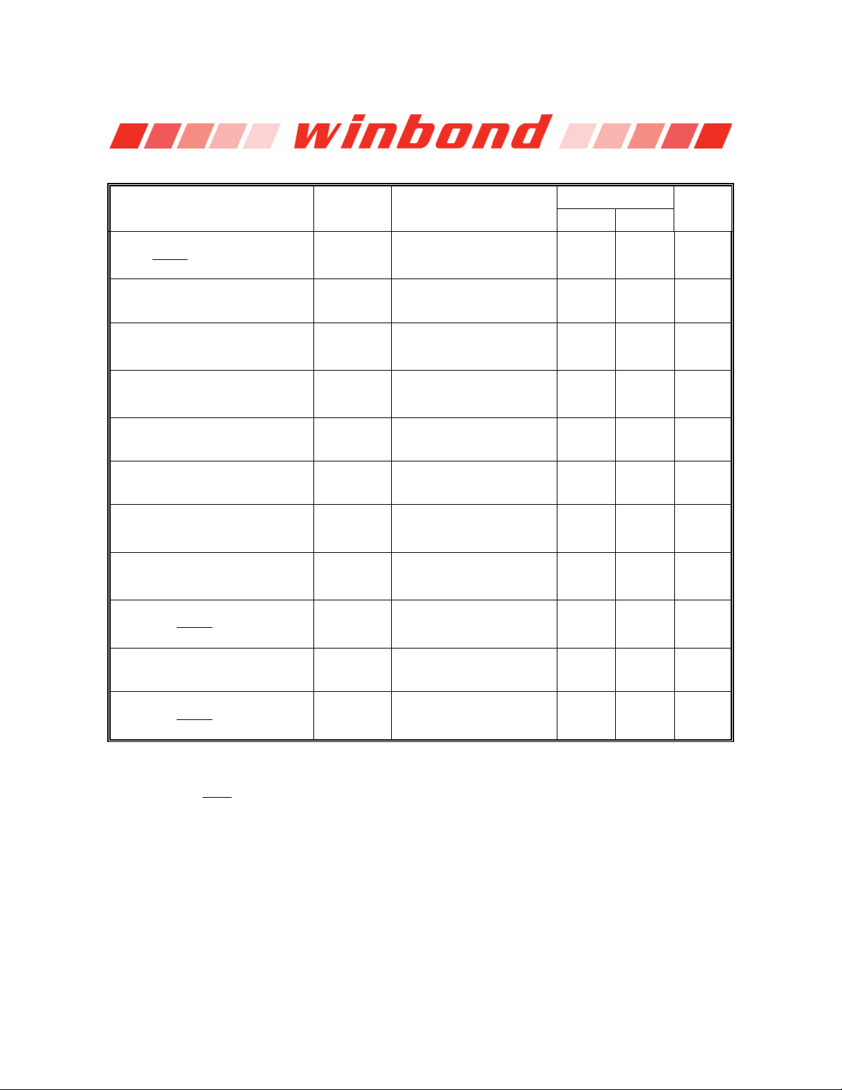
PARAMETER SYMBOL TEST CONDITIONS
Output High Voltage
ALE,
PSEN
, P0
(*3)
Input Low Voltage
(Except RST)
= 4.5V
V
DD
OH2
V
V
IL1 VDD = 4.5V 0 0.8 V
OH2
I
= -400 μA
PECIFICATION
MIN. MAX.
UNIT
2.4 - V
Input Low Voltage
IL2 VDD = 4.5V 0 0.8 V
RST
(*4)
V
Input Low Voltage
IL3 VDD = 4.5V 0 0.8 V
XTAL1
(*4)
Input High Voltage
(Except RST)
Sink Current
P1, P2, P3, P4
Input High Voltage
(*4)
RST
Input High Voltage
XTAL1
(*4)
Sink Current
P0, ALE,
PSEN
(*3)
Source Current
P1, P2, P3, P4
Source Current
P0, ALE,
Notes:
*1. Pins P1, P2 and P3 source a transition current when they are being externally driven from 1 to 0. The transition current
*2. RST pin has an internal pull-down resistor.
*3. P0, ALE,
*4. XTAL1 is a CMOS input and RST is a Schmitt trigger input.
PSEN
reaches its maximum value when VIN is approximately 2V.
(*3)
PSEN
are in the external access memory mode.
V
V
IH1 VDD = 4.5V 2.4
V
I
SK1
IH2 VDD
V
IH3 VDD = 4.5V
V
I
SK2
I
SR1
I
SR2
DD = 4.5V
Vs = 0.45V
= 4.5V
V
DD = 4.5V
Vs = 0.45V
V
DD = 4.5V
Vs = 2.4V
VDD = 4.5V
Vs
= 2.4V
V
DD
+0.2
V
4 12 mA
0.67
DD
V
0.67
DD
V
VDD
+0.2
VDD
+0.2
V
V
8 16 mA
-100 -250 uA
-8 -14 mA
- 14 -
Page 15
W78E54C/W78E054C
7.3 A.C. Characteristics
The AC specifications are a function of the particular process used to manufacture the part, the
ratings of the I/O buffers, the capacitive load, and the internal routing capacitance. Most of the
specifications can be expressed in terms of multiple input clock periods (TCP), and actual parts will
usually experience less than a ±20 nS variation. The numbers below represent the performance
expected from a 0.6micron CMOS process when using 2 and 4 mA output buffers.
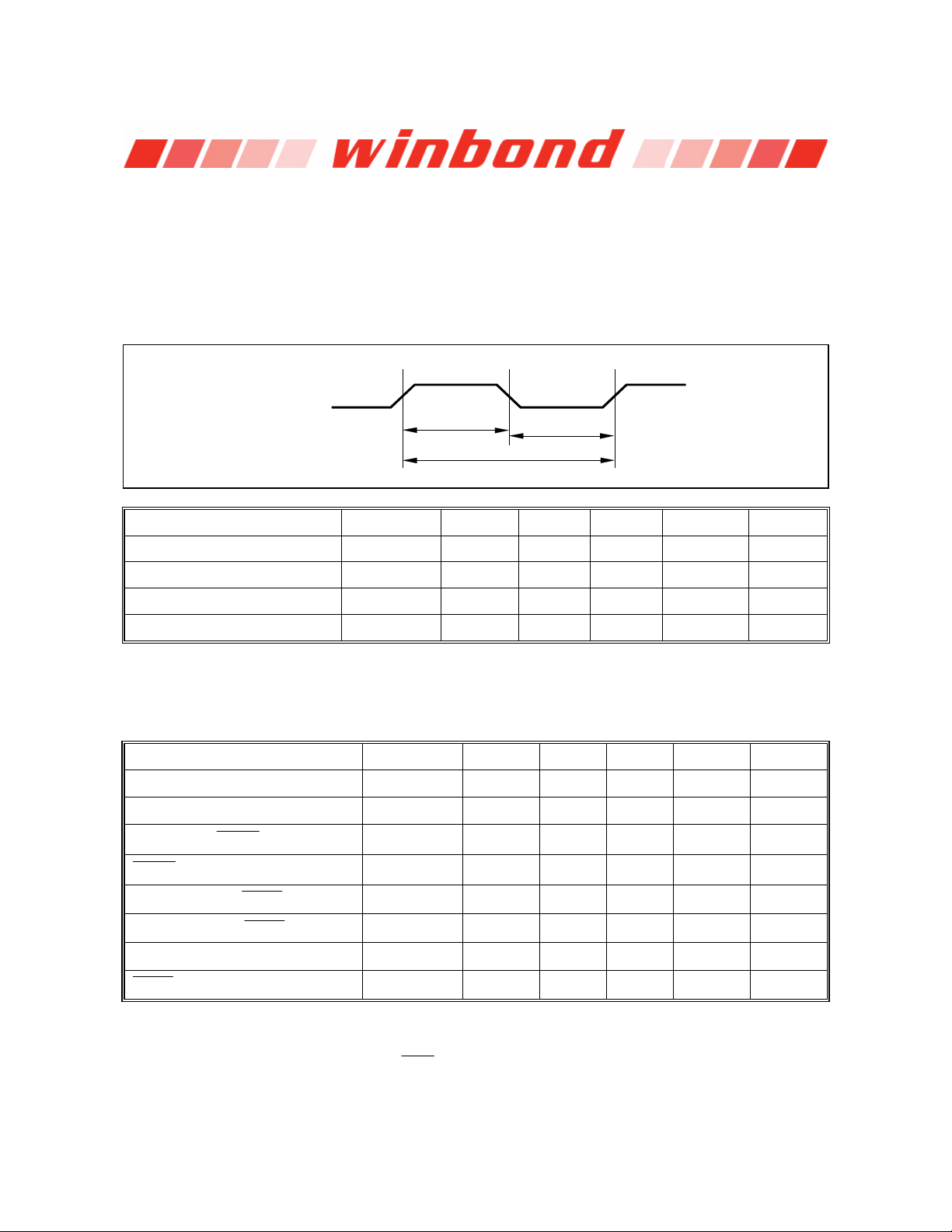
7.3.1 Clock Input Waveform
XTAL1
T
CH
F
OP,
T
CL
T
CP
PARAMETER SYMBOL MIN. TYP. MAX. UNIT NOTES
Operating Speed FOP 0 - 40 MHz 1
Clock Period TCP 25 - - nS 2
Clock High TCH 10 - - nS 3
Clock Low TCL 10 - - nS 3
Notes:
1. The clock may be stopped indefinitely in either state.
2. The T
3. There are no duty cycle requirements on the XTAL1 input.
CP specification is used as a reference in other specifications.
7.3.2 Program Fetch Cycle
PARAMETER SYMBOL MIN. TYP. MAX. UNIT NOTES
Address Valid to ALE Low TAAS
Address Hold from ALE Low TAAH
APL
ALE Low to
PSEN
Low
T
1 T
1 T
1 T
CP -Δ
CP -Δ
CP -Δ
- - nS 4
- - nS 1, 4
- - nS 4
PDA - - 2 TCP nS 2
PSEN
Low to Data Valid
Data Hold after PSEN High
Data Float after PSEN High
ALE Pulse Width TALW
PSEN Pulse Width
Notes:
1. P0.0−P0.7, P2.0−P2.7 remain stable throughout entire memory cycle.
2. Memory access time is 3 T
3. Data have been latched internally prior to
4. "Δ" (due to buffer driving delay and wire loading) is 20 nS.
CP.
T
PDH 0 - 1 TCP nS 3
T
PDZ 0 - 1 TCP nS
T
2 T
CP -Δ
PSW
T
PSEN going high.
3 T
CP -Δ
- 15 - Revision A4
CP - nS 4
2 T
CP - nS 4
3 T
Publication Release Date: October 3, 2006
Page 16
7.3.3 Data Read Cycle
PARAMETER SYMBOL MIN. TYP. MAX. UNIT NOTES
ALE Low to RD Low
RD Low to Data Valid
Data Hold from RD High
Data Float from RD High
W78E54C/W78E054C
DAR
T
DDA - - 4 TCP nS 1
T
DDH 0 - 2 TCP nS
T
DDZ 0 - 2 TCP nS
T
3 T
CP -Δ
-
3 TCP +Δ
nS 1, 2
RD Pulse Width
Notes:
1. Data memory access time is 8 TCP.
2. "
Δ" (due to buffer driving delay and wire loading) is 20 nS.
T
DRD
6 T
CP -Δ
CP - nS 2
6 T
7.3.4 Data Write Cycle
PARAMETER SYMBOL MIN. TYP. MAX. UNIT
DAW
ALE Low to WR Low
Data Valid to WR Low
Data Hold from WR High
WR Pulse Width
Note: "Δ" (due to buffer driving delay and wire loading) is 20 nS.
T
T
DWD
T
DWR
T
DAD
3 T
1 T
1 T
6 T
CP -Δ
CP -Δ
CP -Δ
CP -Δ
-
3 TCP +Δ
nS
- - nS
- - nS
CP - nS
6 T
7.3.5 Port Access Cycle
PARAMETER SYMBOL MIN. TYP. MAX. UNIT
Port Input Setup to ALE Low TPDS 1 TCP - - nS
Port Input Hold from ALE Low TPDH 0 - - nS
Port Output to ALE TPDA 1 TCP - - nS
Note: Ports are read during S5P2, and output data becomes available at the end of S6P2. The timing data are referenced to
ALE, since it provides a convenient reference.
- 16 -
Page 17
7.3.6 Program Operation
PARAMETER SYMBOL MIN. TYP. MAX. UNIT
W78E54C/W78E054C
VPP Setup Time TVPS 2.0 - Data Setup Time TDS 2.0 - Data Hold Time TDH 2.0 - Address Setup Time TAS 2.0 - Address Hold Time TAH 0 - -
CE
Program Pulse Width for Program
Operation
OECTRL Setup Time TOCS 2.0 - OECTRL Hold Time TOCH 2.0 - -
OE
Setup Time
OE
High to Output Float
Data Valid from OE
Note: Flash data can be accessed only in flash mode. The RST pin must pull in VIH status, the ALE pin must pull in VIL status,
and the PSEN pin must pull in VIH status.
T
PWP 290 300 310
TOES 2.0 - -
TDFP 0 - 130 nS
TOEV - - 150 nS
μS
μS
μS
μS
μS
μS
μS
μS
μS
Publication Release Date: October 3, 2006
- 17 - Revision A4
Page 18
8. TIMING WAVEFORMS
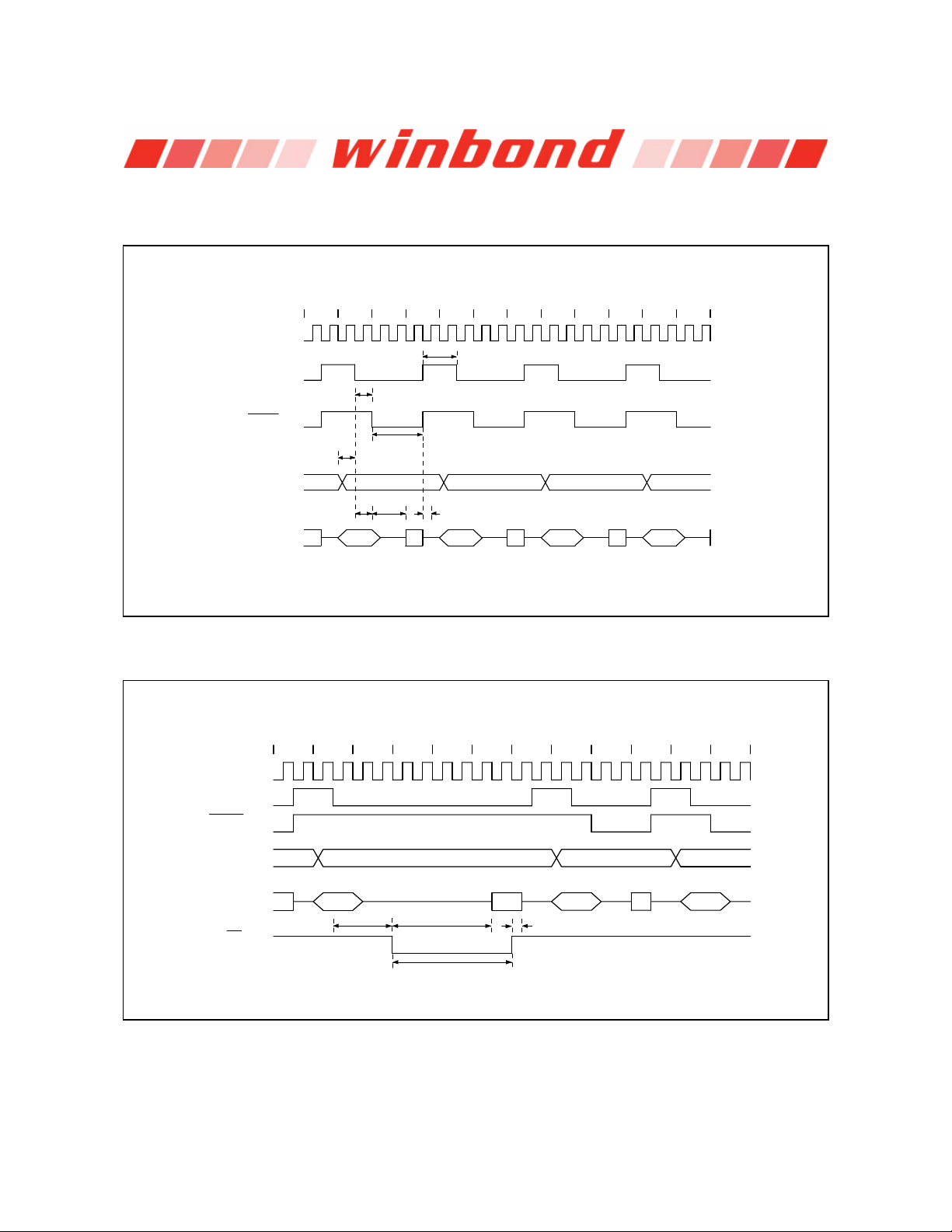
8.1 Program Fetch Cycle
S1
XTAL1
ALE
PSEN
PORT 2
T
AAH
PORT 0
A0-A7
Code
W78E54C/W78E054C
S2 S3 S4 S5 S6 S1 S2 S3 S4 S5 S6
T
ALW
T
APL
T
PSW
T
AAS
T
PDA
Data
T
PDH,TPDZ
A0-A7
Code
A0-A7
Data
A0-A7
8.2 Data Read Cycle
XTAL1
ALE
PSEN
PORT 2
PORT 0
RD
A0-A7
S2 S3S5 S6 S1S2 S3 S4S5 S6 S1S4
A8-A15
DATA
T
DAR
T
DDA
T
DRD
T
DDH,TDDZ
- 18 -
Page 19
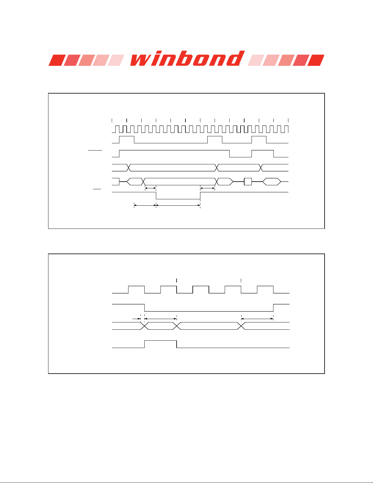
Timing Waveforms, continued
8.3 Data Write Cycle
XTAL1
ALE
PSEN
W78E54C/W78E054C
S2 S3S5 S6 S1S2 S3 S4S1S5 S6S4
PORT 2
PORT 0
WR
8.4 Port Access Cycle
XTAL1
ALE
PORT
INPUT
SAMPLE
T
A8-A15
A0-A7
T
DAW
S5 S6 S1
T
T
PDHPDS
DAD
DATA OUT
T
DWR
T
DWD
T
PDA
DATA OUT
Publication Release Date: October 3, 2006
- 19 - Revision A4
Page 20
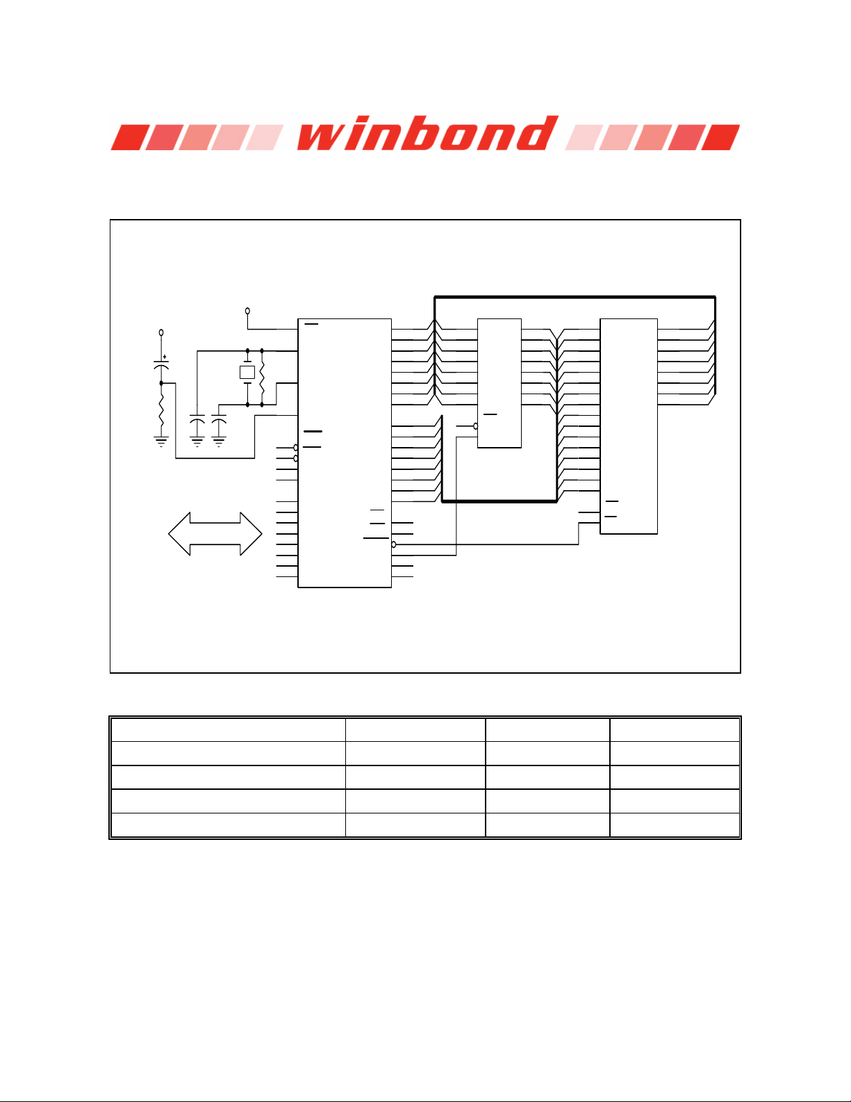
W78E54C/W78E054C
9. TYPICAL APPLICATION CIRCUITS
9.1 Expanded External Program Memory and Crystal
V
DD
V
8.2 K
DD
10 u
C1
CRYSTAL
C2
R
18
9
12
13
14
15
1
2
3
4
5
6
7
8
31
19
EA
XTAL1
XTAL2
RST
INT0
INT1
T0
T1
P1.0
P1.1
P1.2
P1.3
P1.4
P1.5
P1.6
P1.7
W78E54B
P0.0
P0.1
P0.2
P0.3
P0.4
P0.5
P0.6
P0.7
P2.0
P2.1
P2.2
P2.3
P2.4
P2.5
P2.6
P2.7
RD
WR
PSEN
ALE
TXD
RXD
38
37
39
36
35
33
21
22
23
24
25
26
27
28
34
32
17
16
29
30
11
10
AD0
AD1
AD2
AD3
AD4
AD5
AD6
AD7
A8
A9
A10
A11
A12
A13
A14
A15
AD0
AD1
AD2
AD3
AD4
AD5
AD6
AD7
GND
3
4
7
8
13
14
17
18
1
11
D0
D1
D2
D3
D4
D5
D6
D7
OC
G
74373
Q0
Q1
Q2
Q3
Q4
Q5
Q6
Q7
2
5
6
9
12
15
16
19
A0
A1
A2
A3
A4
A5
A6
A7
A0
A1
A2
A3
A4
A5
A6
A7
A8
A9
A10
A11
A12
A13
A14
A15
GND
10
9
8
7
6
5
4
3
25
24
21
23
2
26
27
1
20
22
A0
A1
A2
A3
A4
A5
A6
A7
A8
A9
A10
A11
A12
A13
A14
A15
CE
OE
27512
O0
O1
O2
O3
O4
O5
O6
O7
11
12
13
15
16
17
18
19
AD0
AD1
AD2
AD3
AD4
AD5
AD6
AD7
CRYSTAL C1 C2 R
16 MHz 30P 30P 24 MHz 15P 15P 33 MHz 10P 10P 6.8K
40 MHz 5P 5P 4.7K
Above table shows the reference values for crystal applications (full gain).
Note:
C1, C2, R components refer to Figure A.
Figure A
- 20 -
Page 21
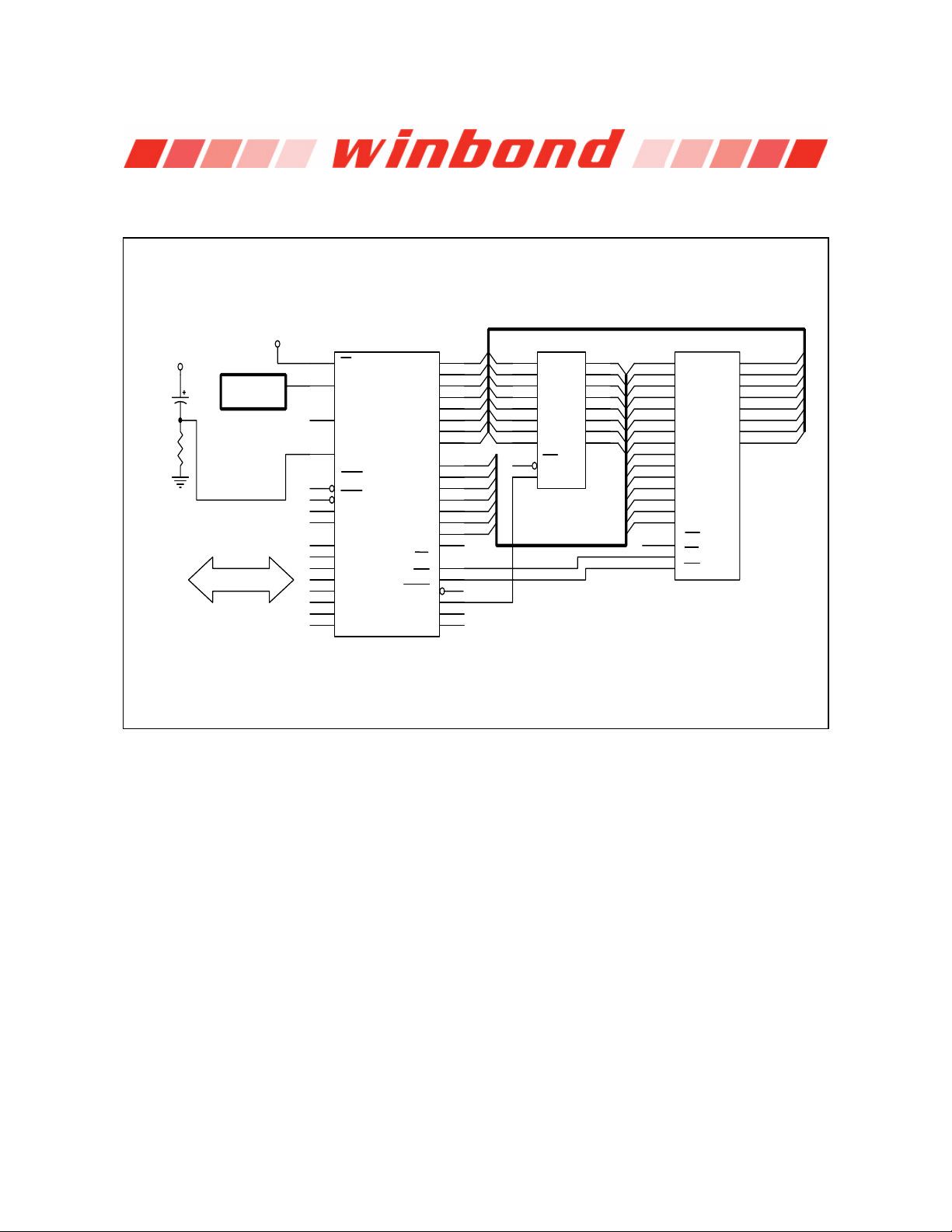
Typical Application Circuits, continued
9.2 Expanded External Data Memory and Oscillator
V
DD
V
8.2 K
DD
10 u
OSCILLATOR
31
19
18
9
12
13
14
15
1
2
3
4
5
6
7
8
EA
XTAL1
XTAL2
RST
INT0
INT1
T0
T1
P1.0
P1.1
P1.2
P1.3
P1.4
P1.5
P1.6
P1.7
W78E54B
P0.0
P0.1
P0.2
P0.3
P0.4
P0.5
P0.6
P0.7
P2.0
P2.1
P2.2
P2.3
P2.4
P2.5
P2.6
P2.7
RD
WR
PSEN
ALE
TXD
RXD
AD0
39
AD0
AD1
38
AD2
37
AD3
36
AD4
35
AD5
34
33
AD6
32
AD7
21
A8
A9
22
23
A10
24
A11
25
A12
26
A13
27
A14
28
17
16
29
30
11
10
AD1
AD2
AD3
AD4
AD5
AD6
AD7
GND
3
4
7
8
13
14
17
18
11
D0
D1
D2
D3
D4
D5
D6
D7
1
OC
G
74373
W78E54C/W78E054C
10
Q0
Q1
Q2
Q3
Q4
Q5
Q6
Q7
2
A1
A2
A3
A4
A5
A6
A7
A1
A2
A3
A4
A5
A6
A7
A8
A9
A10
A11
A12
A13
A14
GND
5
6
9
12
15
16
19
A0
A1
A2
A3
A4
A5
A6
A7
A8
A9
A10
A11
A12
A13
A14
CE
OE
WR
20256
D0
D1
D2
D3
D4
D5
D6
D7
9
8
7
6
5
4
3
25
24
21
23
2
26
1
20
22
27
A0
A0
AD0
11
AD1
12
AD2
13
AD3
15
AD4
16
AD5
17
AD6
18
AD7
19
Figure B
Publication Release Date: October 3, 2006
- 21 - Revision A4
Page 22
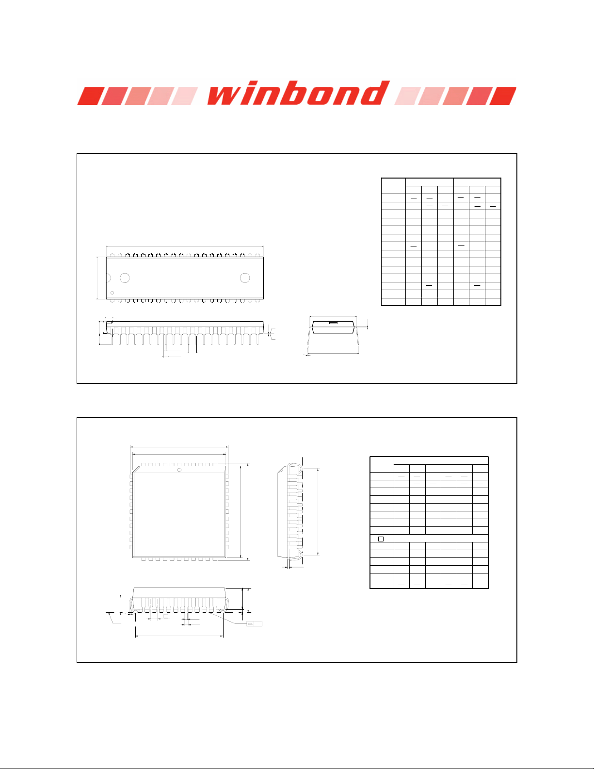
10. PACKAGE DIMENSIONS
10.1 40-pin DIP
40
1
E
1
S
A
2
A
L
D
B
e
1
B
1
W78E54C/W78E054C
Dimension in inch Dimension in mm
Symbol
A
A
A
B
B
c
21
D
E
E
e
L
a
e
20
Base Plane
1
A
Seating Plane
E
e
a
A
S
Notes:
1. Dimension D Max. & S include mold flash or
tie bar burrs.
c
2. Dimension E1 does not include interlead flash.
3. Dimension D & E1 include mold mismatch and
are determined at the mold parting line.
4. Dimension B1 does not include dambar
protrusion/intrusion.
5. Controlling dimension: Inches.
6. General appearance spec. should be based on
final visual inspection spec.
Nom.
Min.
0.010
1
0.155
0.150
2
0.016
0.018
0.050 1.27
1
0.010
0.008
2.055 2.070
0.6000.590
0.540
0.545
1
1
0.120
0.130
015
0.630 16.00
0.650
A
Min.
0.254
3.81
0.406
0.203
14.986
13.72
2.286 2.54 2.7940.090 0.100
3.048
Nom.
3.937
0.457
0.254
52.20
15.24
13.84
3.302
16.51
5.334
4.064
0.559
1.3721.219
0.356
52.58
15.494
13.97
3.556
17.01
Max. Max.
0.210
0.160
0.022
0.0540.048
0.014
0.610
0.550
0.110
0.140
0.670
0.090
.
150
2.286
10.2 44-pin PLCC
61
7
17
L
θ
Seating Plane
e
H
D
D
44 40
G
D
Dimension in inch Dimension in mm
Symbol
39
H
E
E
29
2818
2A
A
b
b
1
A
1
y
G
E
c
A
A
A
b
b
c
D
E
e
G
G
H
H
L
y
Notes:
1. Dimension D & E do not include interlead
flash.
2. Dimension b1 does not include dambar
protrusion/intrusion.
3. Controlling dimension: Inches
4. General appearance spec. should be based
on final visual inspection spec.
Nom.
Min.
0.020
1
0.145
2
0.026
1
0.016
0.008
0.648
0.648
0.590
D
0.590
E
0.680
D
0.680
E
0.090
Max. Max.
0.185
0.150
0.155
0.028
0.032
0.022
0.018
0.014
0.010
0.658
0.653
0.653
0.658
BSC
0.050
0.630
0.610
0.6300.610
0.700
0.690
0.700
0.690
0.100
0.110
0.004
Min.
0.508
3.683
0.66
0.406
0.203
16.46
16.46
14.99
17.27
17.27
2.296
1.27
Nom.
3.81
0.711
0.457
0.254
16.59
16.59
15.49
15.4914.99
17.53
2.54
BSC
4.699
3.937
0.813
0.559
0.356
16.71
16.71
16.00
16.00
17.78
17.7817.53
2.794
0.10
- 22 -
Page 23
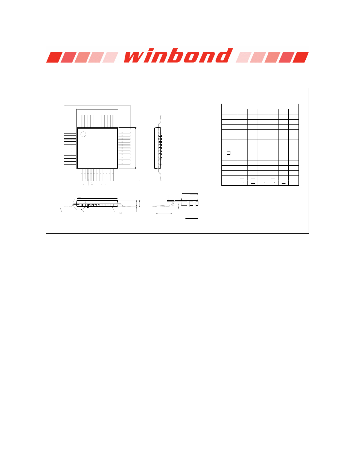
Package Dimensions, continued
10.3 44-pin PQFP
H
D
D
44
1
11
12
e
b
Seating Plane
See Detail F
W78E54C/W78E054C
Dimension in inch
34
33
Symbol
A
A
A
b
1
2
c
D
E
E
H
E
e
D
H
E
H
L
1
L
22
c
A
A
2
A
1
y
θ
L
1
L
Detail F
y
θ
Notes:
1. Dimension D & E do not include interlead
flash.
2. Dimension b does not include dambar
protrusion/intrusion.
3. Controlling dimension: Millimeter
4. General appearance spec. should be based
on final visual inspection spec.
Nom.
Min.
--- ---
---
0.002
0.01 0.02 0.25
0.081
0.075
0.01
0.014
0.006 0.152
0.394
0.390
0.390
0.025
0.031
0.510 13.45
0.520
0.520
0.510
0.025
0.031
0.063
0.051
0
Dimension in mm
Min.
---
0.05
1.90
0.25
9.9
9.9
0.635
12.95
12.95
0.65
Nom.
---
0.5
2.05
2.20
0.45
0.35
0.2540.101
10.00
10.1
10.1
10.00
0.952
0.80
13.2
13.45
13.2
0.8
0.95
1.6
1.905
0
0.08
Max. Max.
---
0.087
0.018
0.0100.004
0.398
0.3980.394
0.036
0.530
0.530
0.037
0.075 1.295
0.003
7
7
Publication Release Date: October 3, 2006
- 23 - Revision A4
Page 24
W78E54C/W78E054C
11. REVISION HISTORY
VERSION DATE PAGE DESCRIPTION
A1 Nov. 26, 2004 - Formerly issued
A2 April 20, 2005 24 Add Important Notice
A3 May 17, 2005 3 Add Lead Free (RoHS) parts
A4 October 3, 2006
Winbond products are not designed, intended, authorized or warranted for use as components
in systems or equipment intended for surgical implantation, atomic energy control
instruments, airplane or spaceship instruments, transportation instruments, traffic signal
instruments, combustion control instruments, or for other applications intended to support or
sustain life. Further more, Winbond products are not intended for applications wherein failure
of Winbond products could result or lead to a situation wherein personal injury, death or
severe property or environmental damage could occur.
Winbond customers using or selling these products for use in such applications do so at their
own risk and agree to fully indemnify Winbond for any damages resulting from such improper
use or sales.
Remove block diagram
3 Remove all Leaded parts
Important Notice
- 24 -
 Loading...