

Page 1

查询W78E354供应商
W78E354
MONITOR MICROCONTROLLER
GENERAL DESCRIPTION
The W78E354 is a stand-alone high-performance microcontroller ASIC specially designed for use in
monitor control applications. Using the Winbond 0.8µ DPDM process, the W78E354 integrates an
embedded 8031 microcontroller core, 16K bytes of Flash cell, 512 bytes of RAM and a number of
dedicated hardware functions. These hardware functions include a 6-bit A/D converter, two/fourteen
12/8-bit PWM static DACs, one/three 12/8-bit PWM dynamic DACs, a sync processor, one DDC port,
a watchdog timer and other custom glue logic. Additional special function registers are incorporated to
control the on-chip peripheral hardware.
The chip is used to control the interface signals of other devices in the monitor and to process the
video sync signals. Because of high integration and the incorporation of Flash cell for program
memory, the device offers the user the competitive advantages of low cost and reduced development
time.
FEATURES
• 80C31 MCU core included
• 16K bytes Flash OTP memory for program storage
• Total 512 bytes of on-chip data RAM:
256 bytes accessed as in the 80C32, 256 bytes accessed as external data memory via "MOVX
@Ri".
• One SPI/RS232 port (a serial port of 8051 standard)
• One external interrupt input
• Two timers/counters
• PWM DACs:
− Two 12-bit PWM/BRM Static DACs
− Fourteen 8-bit PWM Static DACs
− One 12-bit PWM/BRM Dynamic DAC
− Three 8-bit PWM Dynamic DACs
• One 6-bit ADC with 4 multiplexed analog inputs
• Sync Processor:
− Horizontal & Vertical Polarity Detector
− Sync Separator for composite sync
− Horizontal & Vertical Frequency Counter
− Programmable dummy frequency generator
− Programmable H-clamp pulse output
− SOA output (hardware H frequency change detection)
• One DDC port (master/slave mode I
• One 8-bit Auto-reload timer for software time base
2
C with two slave address reg., support DC1/DDC2B/DDC2B+)
Publication Release Date: April 1997
- 1 - Revision A1
Page 2

• Watchdog Timer
132149876
5
3
0
5
1
6
5
6
7
8
9
7
D
4
3
2
4
3
1
• Two 15 mA output pins for driving LEDs
• Power down reset
• Clock: DC to 20 MHz
• Packaged in 68-pin PLCC, 48-pin DIP and 40-pin DIP
PIN CONFIGURATIONS
P
P
2
2
.
.
5
4
/
/
S
S
D
D
A
A
C
A
C
1
1
S
S
S
S
S
D
P
D
P
D
D
D
A
A
A
C
C
C
4
A
4
C
V
.
C
.
D
W78E354
S
S
S
P
D
3
A
A
.
C
S
D
D
P
P
D
A
4
3
A
C
C
.
.
C
SDAC10
SDAC11
P2.6/SDAC12
P2.7/SDAC13
OSCOUT
OSCIN
VSS
P2.0
P2.1
SDAC12
SDAC13
P2.2
P2.3/STP
P3.4/T0
P3.5/T1
HIN
VIN
676866656463626
10
11
12
13
14
15
16
17
18
19
20
21
22
23
24
25
26 44
272829303132333435363738394041424
V
H
B
O
O
S
U
U
D
T
T
A
C
0
P
B
3
S
.
D
0
A
/
C
R
1
X
D
W78E354P
(PLCC-68)
V
P
V
R
S
3
1
T
X
D
S
E
S
.
S
S
A
E
/
T
A
V
A
A
D
C
0
A
A
D
D
D
A
C
C
C
1
2
3
/
/
P
P
1
1
.
.
7
6
59
58
57
56
55
54
53
52
51
50
49
48
47
46
45
P
P
T
3
3
e
.
.
s
2
6
t
/
C
I
L
N
K
T
0
60
SDAC0
BDDAC
DDAC2
DDAC1
DDAC0
P4.3
VPP
P4.2
VDD
P1.5/SOA
P1.4/HCLAMP
P1.3/DSDA
P1.2/DSCL
P1.1
P1.0
P4.1
P4.0
- 2 -
Page 3

Pin Cinfigurations, continued
SDAC5
SDAC6
SDAC7
P2.4/SDAC10
P2.5/SDAC11
P2.6/SDAC12
P2.7/SDAC13
OSCOUT
OSCIN
VSS
P2.0
P2.1
P2.2
P2.3/STP
P3.4/T0
P3.5/T1
HIN
VIN
HOUT
VOUT
BSDAC0
P3.0/RXD
P3.1/TXD
RESET
W78E354
V
1
2
3
4
5
6
7
8
9
10
11
12
13
14
15
16
17
18
19
20
21
22
23
24
48
47
46
45
44
43
42
41
40
39
38
37
36
35
34
33
32
31
30
29
28
27
26
25
DD
SDAC4
SDAC3
SDAC2
SDAC1
P3.3
SDAC0
BDDAC
DDAC2
DDAC1
DDAC0
V
PP
P1.5/SOA
P1.4/HCLAMP
P1.3/DSDA
P1.2/DSCL
P1.1
P1.0
P3.6
P3.2/INT0
TestCLK
VAA
ADC0
VSSA
SDAC5
SDAC6
SDAC7
P2.4/SDAC10
P2.5/SDAC11
P2.6/SDAC12
P2.7/SDAC13
OSCOUT
OSCIN
V
P2.0
P2.1
P2.2
P2.3/STP
HIN
VIN
HOUT
VOUT
BSDAC0
P3.0/RXD
DD
V
1
2
3
4
5
6
7
8
9
10
SS
11
12
13
14
15
16
17
18
19
20
40
39
38
37
36
35
34
33
32
31
30
29
28
27
26
25
24
23
22
21
SDAC4
SDAC3
SDAC2
SDAC1
SDAC0
BDDAC
DDAC0
V
PP
P1.5/SOA
P1.4/HCLAMP
P1.3/DSDA
P1.2/DSCL
P1.1
P1.0
P3.2/INT0
TestCLK
ADC0
RESET
P3.1/TXD
PIN DESCRIPTION
PIN NO.
35
36
37
38
39
1
2
3
-
-
-
-
-
-
NAME
SDAC0
SDAC1
SDAC2
SDAC3
SDAC4
SDAC5
SDAC6
SDAC7
SDAC8
SDAC9
SDAC10
SDAC11
SDAC12
SDAC13
68P 64P 48P 40P
60
57
42
62
59
44
63
60
45
65
61
46
66
62
47
3
1
1
4
2
2
5
3
3
6
4
-
7
5
-
10
8
-
11
9
-
19
17
-
20
18
-
W78E354E
(DIP-48)
PIN
I/O
TYPE
I/O
O/P
TEST
NAME
A0
A1
A2
A3
A4
A5
A6
A7
-
-
-
-
-
-
W78E354
(DIP-40)
FUNCTIONAL DESCRIPTION
8-bit PWM static DAC output.
Sink/Source current 4 mA/-4 mA.
With slew rate control and output delay:
1. Delay about 5 nS:
SDAC2, 5, 8, 11.
2. Delay about 10 nS:
SDAC0, 3, 6, 9, 12.
3. Without delay: the others.
--------------------------------------------------------* In the Flash/RAM-test mode
(when the chip is in reset state):
SDAC0−7: A0−A7 inputs.
* In the functional test mode
(CPU executes out of ext. program memory):
SDAC0−7: A0−A7 outputs.
Publication Release Date: April 1997
- 3 - Revision A1
Page 4

Pin Description, continued
W78E354
PIN NO.
68P 64P 48P 40P
2930272821-19-BSDAC0
56
53
38
33
57
54
39
58
55
40
59 56 41 34 BDDAC I/O A10 12-bit PWM/BRM dynamic DAC output.
-
-
PIN
NAME
BSDAC1
DDAC0
DDAC1
DDAC2
I/O
TYPE
I/O
O/P
I/O
O/P
TEST
NAME
A8
-
A9
-
-
FUNCTIONAL DESCRIPTION
12-bit PWM/BRM static DAC output.
Sink/Source current 8 mA/-8 mA.
With slew rate control and output delay:
1. Delay about 5ns: BSDAC1
2. Without delay: BSDAC0.
--------------------------------------------------------* In the Flash/RAM-test mode
(when the chip is in reset state):
BSDAC0: A8 input.
* In the functional test mode
(CPU executes out of ext. program memory):
BSDAC0: A8 output.
8-bit PWM dynamic DAC output.
Sink/Source current 8 mA/-8 mA.
With slew rate control and output delay:
1. Delay about 5 nS: DDAC1.
2. Delay about 10 nS: DDAC2.
3. Without delay: DDAC0.
--------------------------------------------------------* In the Flash/RAM-test mode
(when the chip is in reset state):
DDAC0: A9 input.
* In the functional test mode
(CPU executes out of ext. program memory):
DDAC0: A9 output.
Sink/Source current 8mA/-8mA.
With slew rate control.
--------------------------------------------------------* In the Flash/RAM-test mode
(when the chip is in reset state):
BDDAC: A10 input.
* In the functional test mode
(CPU executes out of ext. program memory):
BDDAC: A10 output.
- 4 -
Page 5

Pin Description, continued
W78E354
PIN NO.
68P 64P 48P 40P
36
34
26
37
35
-
39
37
-
40
38
-
46474445313226
48494647333428
23
27
29
PIN
NAME
ADC0
-
ADC1
-
ADC2
(P1.6)
ADC3
(P1.7)
P1.0
P1.1
P1.2
(DSCL)
P1.3
(DSDA)
I/O
TYPE
I/P -
I/O A13
I/O A13CTRL
TEST
NAME
A14
A14CTRL
FUNCTIONAL DESCRIPTION
Analog signal input channel to ADC.
-
-
-
Alternate function:
ADC2: P1.6 input (input only).
ADC3: P1.7 input (input only).
General purpose I/O.
Open-drain, Sink current 2mA.
Schmitt trigger I/P.
No PMOS ESD cell.
VIH = 3.0V (min), VIL = 1.5V (max)
--------------------------------------------------------* In the Flash/RAM-test mode
(when the chip is in reset state):
P1.0 and P1.1: A13 and A14 inputs.
* In the functional test mode
(CPU executes out of ext. program memory):
P1.0 and P1.1: do not output A13 and A14, but function in
their normal operational state.
General purpose I/O.
Open-drain, Sink current 6mA.
Schmitt trigger I/P.
No PMOS ESD cell.
VIH = 3.0V (min), VIL = 1.5V (max)
Alternate function:
P1.2: DDC port serial clock DSCL.
P1.3: DDC port serial data DSDA.
--------------------------------------------------------* In the Flash/RAM-test mode
(when the chip is in reset state):
P1.2: A13CTRL input.
P1.3: A14CTRL input.
Publication Release Date: April 1997
- 5 - Revision A1
Page 6

Pin Description, continued
W78E354
PIN NO.
68P 64P 48P 40P
50 48 35 30 P1.4
51 49 36 31 P1.5
17181516111211
12
PIN
NAME
(HCLAMP)
(SOA)
P2.0
P2.1
I/O
TYPE
I/O A9CTRL General purpose I/O.
I/O A11 General purpose O/P.
I/O D0
TEST
NAME
D1
FUNCTIONAL DESCRIPTION
Sink/Source current 4 mA/-100 µA.
Alternate function:
P1.4: HCLAMP (H-clamp pulse) output.
While outputing special function, P1.4's Sink/Source
current is 4 mA/-4 mA.
--------------------------------------------------------* In the Flash/RAM-test mode
(when the chip is in reset state):
P1.4: A9CTRL input.
Sink/Source current 4 mA/-4 mA.
Alternate function:
P1.5: SOA (Safe Operation Area) outpout.
--------------------------------------------------------* In the Flash/RAM-test mode
(when the chip is in reset state):
P1.5: A11 input.
* In the functional test mode
(CPU executes out of ext. program memory):
P1.5: doesn't output A11, but functions as
its normal operation.
General purpose I/O.
Sink/Source current 15mA/-100µA.
With slew rate control .
--------------------------------------------------------* In the Flash/RAM-test mode
(when the chip is in reset state):
P2.0−P2.1: D0−D1 data inputs/outputs.
* In the functional test mode
(CPU executes out of ext. program memory):
P2.0−P2.1: D0−D1 program inputs.
- 6 -
Page 7

Pin Description, continued
W78E354
PIN NO.
68P 64P 48P 40P
21
19
13
20
22
8
9
12
13
31
32
42
61
23
24
43
67
10
11
29
30
40
58
21
22
41
63
14
6
4
7
5
6
7
22
23
29
43
15
16
30
-
13
14
4
5
6
7
20
21
25
-
-
-
-
-
PIN
NAME
P2.2
P2.3
(STP)
P2.4
(SDAC10)
P2.5
(SDAC11)
P2.6
(SDAC12)
P2.7
(SDAC13)
P3.0
(RXD)
P3.1
(TXD)
P3.2
(INT0)
P3.3
P3.4 (T0)
P3.5 (T1)
P3.6
P3.7
I/O
TYPE
I/O D2
I/O -
TEST
NAME
D3
D4
D5
D6
D7
-
A12
(PSEN)
-
-
-
-
-
FUNCTIONAL DESCRIPTION
General purpose I/O.
Sink/Source current 4 mA/-100 µA.
Alternate function:
P2.3: STP (Self-Test Pattern) output.
P2.4−P2.7: SDAC10−13 outputs.
While outputing special function, P2.3−P2.7's
Sink/Source current is 4mA/-4mA.
--------------------------------------------------------* In the Flash/RAM-test mode
(when the chip is in reset state):
P2.2−P2.7: D2−D7 data inputs/outputs.
* In the functional test mode
(CPU executes out of ext. program memory):
P2.2−P2.7: D2−D7 program inputs.
General purpose I/O.
Sink/Source current 2 mA/-100 µA.
Alternate function:
P3.0: 8051 serial input port.
P3.1: 8051 serial output port.
P3.2: External interrupt input.
P3.4 and P3.5: Timer/counter 0 and 1 external inputs.
--------------------------------------------------------* In the Flash/RAM-test mode
(when the chip is in reset state):
P3.2: A12 input.
* In the functional test mode
(CPU executes out of ext. program memory):
P3.2: PSEN output (the read strobe to
external program memory) instead of A12.
Publication Release Date: April 1997
- 7 - Revision A1
Page 8

Pin Description, continued
W78E354
PIN NO.
68P 64P 48P 40P
44
42
-
45
43
-
53
51
-
55
-
-
64
-
-
1
-
-
2
-
-
25262324171815
16
27282526192017
18
33 31 24 22
41 39 28 24 TestCLK I/P
PIN
NAME
-
P4.0
-
P4.1
-
P4.2
-
P4.3
-
P4.4
-
P4.5
-
P4.6
HIN
VIN
HOUT
VOUT
RESET
I/O
TYPE
O/P -
I/P
I/O OECTRL
I/P - Reset the controller (active low).
TEST
NAME
-
-
-
-
-
-
OE
CE
PROG
EA
FUNCTIONAL DESCRIPTION
Output port (Latch output).
Sink/Source current 2 mA/-2 mA.
HIN: Hsync/Composite sync input.
VIN: Vsync input.
Schmitt trigger I/P.
With Internal high value pull-down (about 200 KΩ).
No PMOS ESD diode.
--------------------------------------------------------* In the Flash/RAM-test mode
(when the chip is in reset state):
HIN: OE input.
VIN: CE input.
HOUT: Hsync output.
VOUT: Vsync output with internal weak pull-up (above 200
KΩ).
Sink/Source current 4 mA/-4 mA.
--------------------------------------------------------* In the Flash/RAM-test mode
(when the chip is in reset state):
HOUT: OECTRL input.
VOUT: PROG input.
Schmitt trigger I/P.
With internal pull-up (about 30 KΩ).
Clock input while in internal (glue logic's) function test.
With internal pull-up (about 30 KΩ).
--------------------------------------------------------* If the EA (TestCLK) pin is pulled low when the chip is
being reset, and remains low for at least 24 clock periods
after the reset, the CPU will execute from the external
program memory regardless of the PC value. i.e., the CPU is
forced to enter the functional test mode.
- 8 -
Page 9

Pin Description, continued
W78E354
PIN NO.
68P 64P 48P 40P
141512138989OSCOUT
54 52 37 32 VPP - VPP In the Test/Flash mode, this pin is the power supply input for
68 64 48 40 VDD - - Positive digital power supply, +5V.
16 14 10 10 VSS - - Digital ground.
52 50 - - VDD - - Positive digital power supply, +5V.
34 32 - - VSS - - Digital ground.
38 36 27 - VAA - - Positive analog power supply, +5V.
35 33 25 - VSSA - - Analog ground.
PIN
NAME
OSCIN
I/O
TYPE
O/P
I/P
TEST
NAME
-
-
FUNCTIONAL DESCRIPTION
Output from the inverting oscillator amplifier.
Input to the inverting oscillator amplifier.
Freq.: 16 MHz to 24 MHz.
the Flash cell.
Internally connected to the other power source.
Internally connected to the other power source.
Publication Release Date: April 1997
- 9 - Revision A1
Page 10

BLOCK DIAGRAM
W78E354
W78E354
DD
V
RESET
OSCIN
OSCOUT
HIN, VIN
HOUT, VOUT
HCLAMP (P1.4)
SOA (P1.5)
RXD (P3.0)
TXD (P3.1)
T0 (P3.4)
T1 (P3.5)
SS
V
Power
Source
Supervisor
Reset
Circuit
WDT
OSC/Timing
Generator
Sync
Processor
Srial Port
Timer 0
Timer1
Autoload
Timer
8031 MCU core
with 256B
Scratchpad RAM
16KB
Flash ROM
256B
Data Memory
Interrupt
Processor
SDAC
DDAC
ADC
DDC
I/O Port
Vpp
INT0 (P3.2)
SDAC0~13
BSDAC0~1
DDAC0~2
BDDAC
ADC0~3
AA, VSSA
V
DSCL (P1.2)
DSDA (P1.3)
Port 1, 2, 3
(except P1.5)
P1.5, Port 4
- 10 -
Page 11

W78E354
FUNCTIONAL DESCRIPTION
A. 80C31 Core
The W78E354's 80C31 (CMOS MCU) core architecture consists of a CPU surrounded by various
Special Function Registers or SFRs. Some of these SFRs are standard 80C31 registers while others
are new additions, cf. Table 1. The device includes three general purpose I/O ports (P1, P2 and P3),
one output-only port (P4), 256 bytes of scratchpad RAM, two timer/counters (Timer0 and Timer1) and
one 8051 standard serial port. The processor supports 109 different instructions (without "MOVX
A,@DPTR" and "MOVX @DPTR,A") all of which are compatible with those of the MCS-51 family.
One distinguishing feature of the device architecture is the SFR address space into which all the
registers, peripherals and scratchpad RAM are mapped. Many of the instructions operate on an SFR
address rather than a specific register, greatly increasing the power of the instruction set.
The core controller has been designed around a state machine rather than utilizing a microcode
approach, a design methodology which offers several advantages. The first of these is that faster
circuits can be produced due to the fact that flip-flops are inherently faster than ROMs. Secondly, a
ROM-free approach allows the design to be directly utilized in ASIC gate array implementations, an
important factor for cost reductions. Finally, an entire digital logic approach provides better supply
noise immunity in most applications.
Table 1. W78E354's Special Function Registers (SFRs)
F8 FF
F0 + B F7
E8 EF
E0 + ACC E7
D8 + S1CON S1STA S1DAT S1ADR DF
D0 + PSW D7
C8 + CONTREG4 CF
C0 C7
B8 + IP SBRM0 SBRM1 PORT4 SOAREG SOACLR BF
B0 + P3 ADC INTVECT STATUS HFCOUNTL HFCOUNTH VFCOUNTL VFCOUNTH B7
A8 + IE SDAC7 SDAC8 SDAC9 SDAC10 SDAC11 SDAC12 SDAC13 AF
A0 + P2 SDAC0 SDAC1 SDAC2 SDAC3 SDAC4 SDAC5 SDAC6 A7
98 + SCON SBUF BSDAC0 BSDAC1 WDTCLR DDAC0 DDAC1 DDAC2 9F
90 + P1 AUTOLOAD DHREG DVREG DDC1 INTMSK BDDAC DBRM 97
88 + TCON TMOD TL0 TL1 TH0 TH1 PARAL PARAH 8F
80 + CONTREG1 SP DPL DPH CONTREG5 CONTREG2 CONTREG3 PCON 87
Notes:
1. The SFRs with a "+" are both byte- and bit-addressable.
2. The registers in the shaded region are new additions to the 80C31 SFRs.
A.1 Address Space (cf. Figure 1)
The W78E354 CPU operates out of three separate address spaces:
- 11 - Revision A1
Publication Release Date: April 1997
Page 12

W78E354
1. The first of these is the internal program space (internal Flash memory) with 16K byte size
(0000H− 3FFFH). The program space can be accessed by both opcode fetches and the
"MOVC" instructions.
2. The second is referred to as the data memory space and has a size of 256 bytes (0000H−00FFH).
The data memory is integrated within the chip rather than being outside as in the case of the
standard 8031. The "inside" data memory space is accessed by the "MOVX @Ri" instruction.
3. The third address space has 256 locations while it is used by 384 bytes (256 bytes of RAM and 128
bytes of SFRs).
• The lower 128 locations of this address space (00H−7FH) are for the lower 128 bytes of scratchpad
RAM. Any of these 128 bytes may be used by a programmer but some of them have special uses.
The lowest 32 bytes are organized to four 8-byte register banks. The bank select bits (RS0 and RS1
in the PSW register) selects one of these four banks which is to be used currently as an operand in
the instruction set. Registers 0 to 7 in the bank are referenced by the register direct opcodes.
Registers 0 and 1 may also contain an address that is referenced by the register indirect opcodes.
• The higher 128 locations of this address space (80H−FFH) are shared by the higher 128 bytes of
scratchpad RAM and the Special Function Registers (SFRs). The SFRs are accessed only by "direct"
addressing while the higher 128 bytes of scrachpad RAM are accessed only by "indirect" addressing.
The higher 128 bytes of scratchpad data RAM are also available for stack space.
Address spaces 20H to 2FH are bit-addressable and can be used by the Boolean Variable
Manipulation instructions. For example, bit 0 of address 20H has a Boolean address 00H, and bit 7 of
address 2FH has a Boolean address 7FH. The higher Boolean addresses (80H−FFH) are mapped
into the SFR address space. To determine a Boolean address in some bit-addressable SFR, the
higher 5 bits of the SFR's address can be combined with the 3 lower bits that specify the desired bit in
the SFR.
3FFFH
0000H
On-Chip
Program
Memory
On-Chip
Data
Memory
FFH
(MOVX @Ri)
00H
Figure1. Addres Space
- 12 -
FFH
(Direct Addressing)
80H
7FH
00H
SFR
Scratchpad
RAM
(Direct/Indirect
Addressing)
Scratchpad
RAM
(Indirect Addressing)
Page 13

A.2 The Modified 80C31 SFRs
1. Timer/Counter Control Register: TCON
BIT NAME FUNCTION
TCON.7 TF1 Timer 1 overflow flag.
Set by hardware on timer/counter overflow. Cleared by hardware when the
processor vectors to the interrupt routine.
TCON.6 TR1 Timer 1 run control bit.
Set/cleared by software to turn the timer/counter on or off.
TCON.5 TF0 Timer 0 overflow flag.
Set by hardware on timer/counter overflow. Cleared by hardware when the
processor vectors to the interrupt routine.
TCON.4 TR0 Timer 0 run control bit.
Set/cleared by software to turn the timer/counter on or off.
TCON.3 - (Reserved, not used by users.)
TCON.2 - (Reserved)
W78E354
TCON.1 IE0 Interrupt 0 edge flag.
Set by hardware when an external interrupt edge is detected. Cleared when
the interrupt is processed.
TCON.0 IT0 Interrupt 0 type control bit.
Set/cleared by software to specify falling edge/low level triggered external
interrupt.
2. Power Control Register: PCON
BIT NAME FUNCTION
7 SMOD Double baud rate bit.
6 - (Reserved)
5 - (Reserved, not used by users.)
4 - (Reserved for testing, not used by users.
Normally 0. If set, P2.4−P2.7 will output SDAC8-11 after reset (not power-
on reset).)
3 GF1 General-purpose flag bit.
2 GF0 General-purpose flag bit.
1 PD Power-down mode bit.
0 IDL Idle mode bit.
Publication Release Date: April 1997
- 13 - Revision A1
Page 14

3. Interrupt Enable Register: IE
BIT NAME FUNCTION
IE.7 EA
If EA = 0, no interrupt will be acknowledged (disable all interrupts).
If EA = 1, each interrupt source is individually enabled or disabled by setting or
clearing its enable bit.
IE.6 IE.5 *1
IE.4 ES
IE.3 ET1
IE.2 *1
IE.1 ET0
IE.0 EX0
Notes:
*1: No name for ASSEMBLER, must be used via "IE.x".
*2 = (DSCLINT + ADCINT + TIMEOUT + SOAINT + VEVENT + PARAINT + DDC1INT).
(Reserved)
Set/clear to enable/disable the DDC port's I2C interrupt.
Set/clear to enable/disable the serial port 0 interrupt.
Set/clear to enable/disable the Timer 1 overflow interrupt.
Set/clear to enable/disable the *2 interrupt.
Set/clear to enable/disable the Timer 0 overflow interrupt.
Set/clear to enable/disable the external interrupt 0.
W78E354
4. Interrupt Priority Register: IP
BIT NAME FUNCTION
IP.7 - (Reserved)
IP.6 - (Reserved)
IP.5 *1 Define the DDC port's I2C interrupt priority level.
If IP.5 = 1, the priority level is higher.
IP.4 PS Define the serial port interrupt priority level.
If PS = 1, the priority level is higher.
IP.3 PT1 Define the Timer 1 interrupt priority level.
If PT1 = 1, the priority level is higher.
IP.2 *1 Define the *2 priority level.
If IP.2 = 1, the priority level is higher.
IP.1 PT0 Define the Timer 0 interrupt priority level.
If PT0 = 1, the priority level is higher.
IP.0 PX0 Define the external interrupt 0 priority level.
If PX0 = 1, the priority level is higher.
Notes:
*1: No name for ASSEMBLER, must be used via "IP.x".
*2 = (DSCLINT + ADCINT + TIMEOUT + SOAINT + VEVENT + PARAINT + DDC1INT).
- 14 -
Page 15
W78E354
A.3 New Register Description
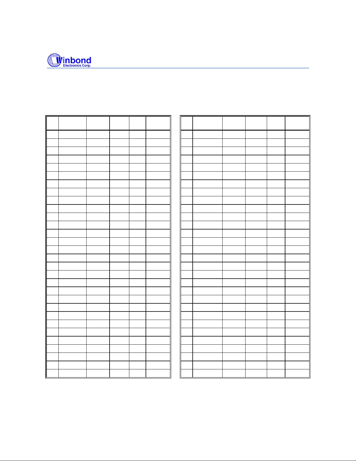
In addition to the 80C31 standard SFRs, the W78E354 has some newly added Special Function
Registers in the SFR address space as listed in Table 2.
Table 2. Newly Added Special Function Registers (SFRs)
REGISTER ADDRESS LENGTH R/W
TYPE
1 CONTREG1 80H 8 R/W 00H 31 VFCOUNTL B6H 8 R 00H
2 CONTREG2 85H 8 W 00H 32 VFCOUNTH B7H 8 R 00H
3 CONTREG3 86H 8 W 00H 33 DHREG 92H 4 W 00H
4 CONTREG4 C8H 8 R/W 00H 34 DVREG 93H 8 W 00H
5 CONTREG5 84H 8 R/W 00H 35 PARAL 8EH 8 W 00H
6 SDAC0 A1H 8 W 00H 36 PARAH 8FH 8 W 00H
7 SDAC1 A2H 8 W 00H 37 AUTOLOAD 91H 8 W 00H
8 SDAC2 A3H 8 W 00H 38 WDTCLR 9CH - W -
9 SDAC3 A4H 8 W 00H 39 SOAREG BCH 8 W 00H
10 SDAC4 A5H 8 W 00H 40 SOACLR BDH - W 11 SDAC5 A6H 8 W 00H 41 INTMSK 95H 8 W 00H
12 SDAC6 A7H 8 W 00H 42 INTVECT B2H 8 R/W 00H
13 SDAC7 A9H 8 W 00H 43 STATUS B3H 4 R 00H
14 SDAC8 AAH 8 W 00H 44 ADC B1H 8 R 80H
15 SDAC9 ABH 8 W 00H 45 PORT4 BBH 7 W 00H
16 SDAC10 ACH 8 W 00H 46 DDC1 94H 8 W 00H
17 SDAC11 ADH 8 W 00H 47 S1CON D8H 8 R/W 00H
18 SDAC12 AEH 8 W 00H 48 S1STA D9H 8 R F8H
19 SDAC13 AFH 8 W 00H 49 S1DAT DAH 8 R/W 00H
20 BSDAC0 9AH 8 W 00H 50 S1ADR DBH 8 R/W 00H
21 SBRM0 B9H 4 W 00H
22 BSDAC1 9BH 8 W 00H
23 SBRM1 BAH 4 W 00H
24 DDAC0 9DH 8 W 00H
25 DDAC1 9EH 8 W 00H
26 DDAC2 9FH 8 W 00H
27 BDDAC 96H 8 W 00H
28 DBRM 97H 4 W 00H
29 HFCOUNTL B4H 8 R 00H
30 HFCOUNTH B5H 8 R 00H
RESET
CONTENT
REGISTER ADDRESS LENGTH R/W
TYPE
RESET
CONTENT
Note: '-' means the SFR has no real hardware but an address.
Publication Release Date: April 1997
- 15 - Revision A1
Page 16
W78E354
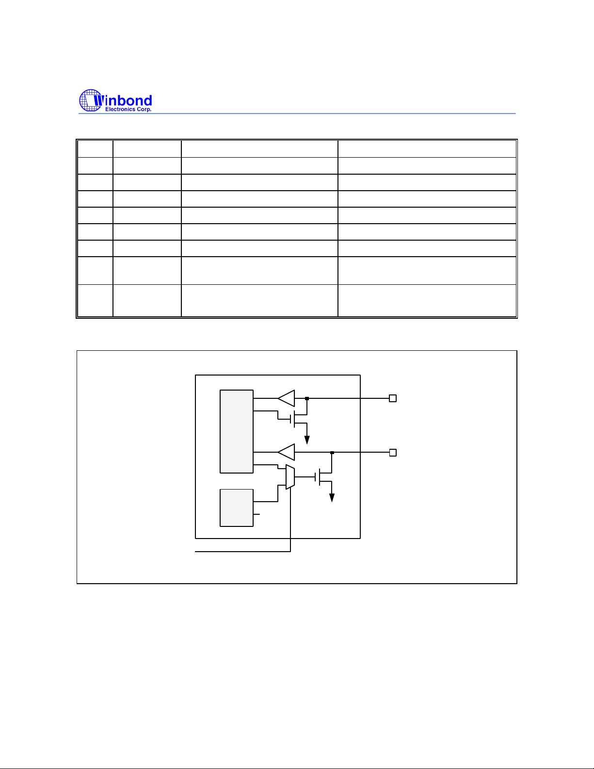
* CONTREG1: Control register1, bit-addressable.
BIT NAME FUNCTION NOTE
0 ADCS0 ADC channel Select bit 0 See Section E.10.
1 ADCS1 ADC channel Select bit 1 See Section E.10.
2 ENDDC1 Enable DDC1 See below.
3 HCES H-Clamp Edge Select See Section E.12.f.
4 HCWS0 H-Clamp Width Select bit 0 See Section E.12.f.
5 HCWS1 H-Clamp Width Select bit 1 See Section E.12.f.
6 DUMMYEN Dummy signal Enable See Section E.12. 'Sync Processor
Block Diagram' & E.12.e.
7 ADCSTRT Start ADC conversion
0: Stop, 1: Start
DDC Port
SCL
SDA
SDA
SCL
IN
OUT
IN
OUT
OUT
from Vsync
2
I C
Support DDC2B/2B+
DDC1
Support DDC1
ENDDC1
See Section E.10.
P1.2/DSCL
P1.3/DSDA
0
1
- 16 -
Page 17
W78E354
0
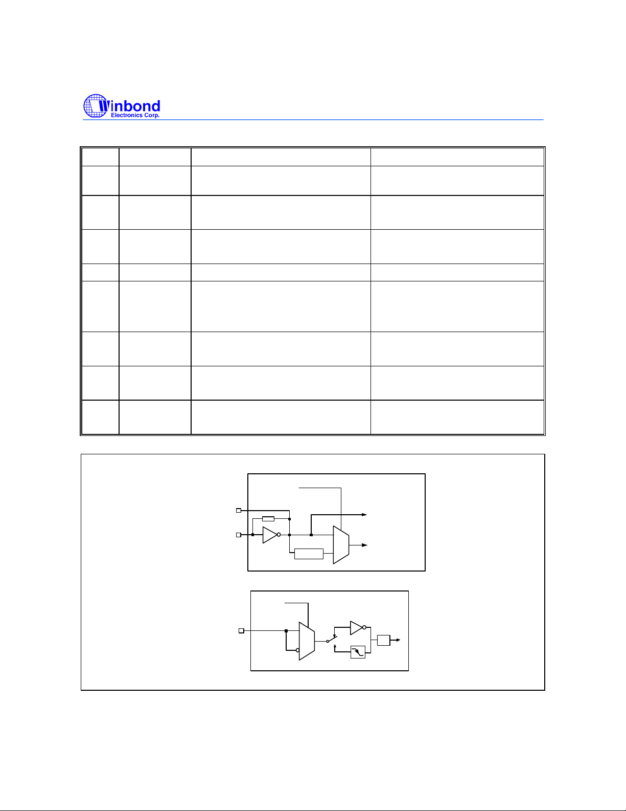
* CONTREG2: Control register2.
BIT NAME FUNCTION NOTE
0 ENVS ENable Vsync Separator See Section E.12. 'Sync Processor
Block Diagram' & E.12.e.
1 HSPS HSync Polarity Select
0: Positive, 1: Negative
2 VSPS VSync Polarity Select
0: Positive, 1: Negative
See Section E.12. 'Sync Processor
Block Diagram'.
See Section E.12. 'Sync Processor
Block Diagram'.
3 OSCSEL OSC or OSC/2 SELect See below.
4 EINTES External INT Edge Select
See below.
0: High-level/rising-edge triggered
1: Low-level/falling-edge triggered
5 ENM0 ENable SDAC0 Moire cancel function
0: Disable, 1:Enable
6 ENM1 ENable SDAC1 Moire cancel function
0: Disable, 1:Enable
7 VDISHC Vsync DISable H-Clamp pulse
0: Enable, 1:Disable
OSCSEL
See Section E.12. 'Sync Processor
Block Diagram'.
OSCOUT
OSCIN
INT0
(P3.2)
EINTES
To CPU core
0
Divided by 2
1
0
1
IT0
1
To Sync processor
IE0
Publication Release Date: April 1997
- 17 - Revision A1
Page 18
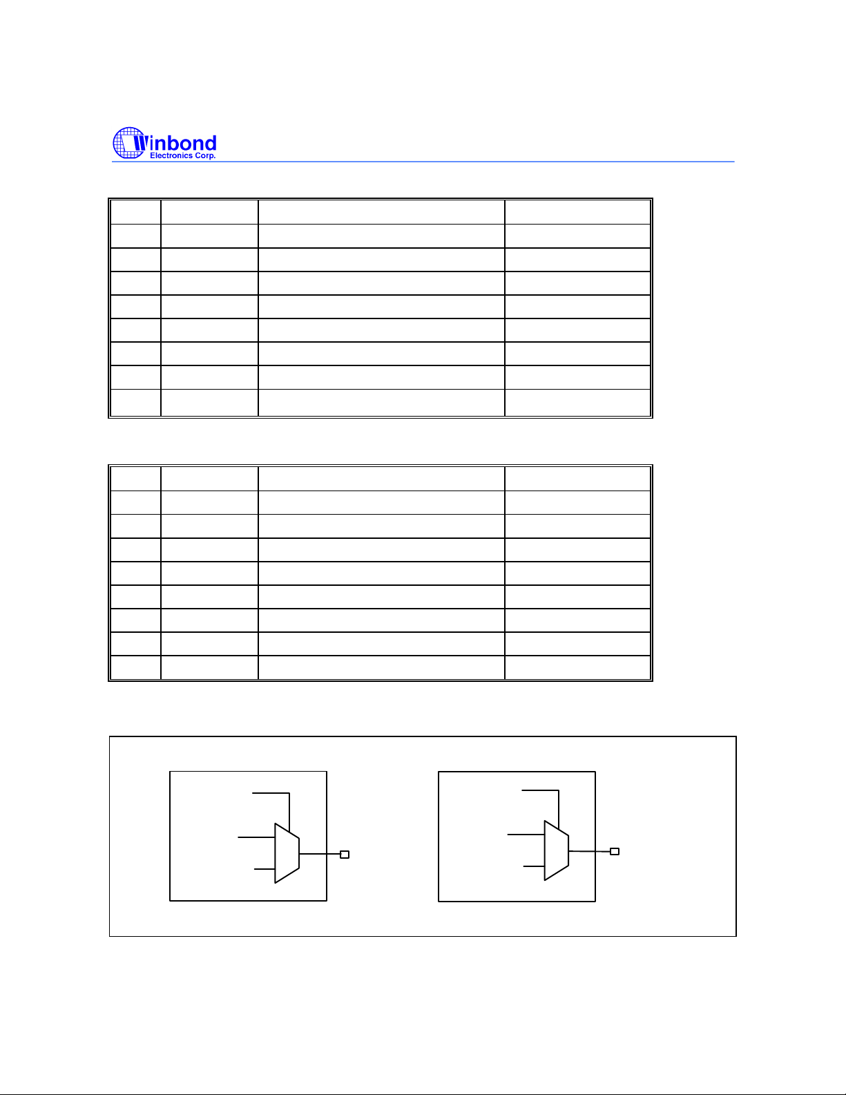
*CONTREG3: Control register3.
BIT NAME FUNCTION NOTE
0 P4SF Port 4 Special Function
1 TSTMOD1 Function test mode1
2 TSTMOD2 Function test mode2
3 TSTMOD3 Function test mode3
4 TVSEP Test VSEP signal
5 - (Reserved for internal use.)
6 - (Reserved for internal use.)
W78E354
7
- (Reserved for internal use.)
*CONTREG4: Control register4, bit-addressable.
BIT NAME FUNCTION NOTE
0 P24SF Port 2.4 Special Function* (SDAC10) See below.
1 P25SF Port 2.5 Special Function* (SDAC11) See below.
2 P26SF Port 2.6 Special Function* (SDAC12) See below.
3 P27SF Port 2.7 Special Function* (SDAC13) See below.
4 P14SF Port 1.4 Special Function* See below.
5 P15SF Port 1.5 Special Function* See below.
6 P23SF Port 2.3 Special Function* See below.
7 INVSTP Invert Self-Test Pattern
*Note:In addition to setting PxySF, the port latch Pxy must have been cleared previously to enable the Pxy output special
functions.
P14SF
P15SF
P1.4 latch
H-Clamp pulse
0
1
P1.4/HCLAMP
P1.5 latch
SOA output
0
P1.5/SOA
1
- 18 -
Page 19
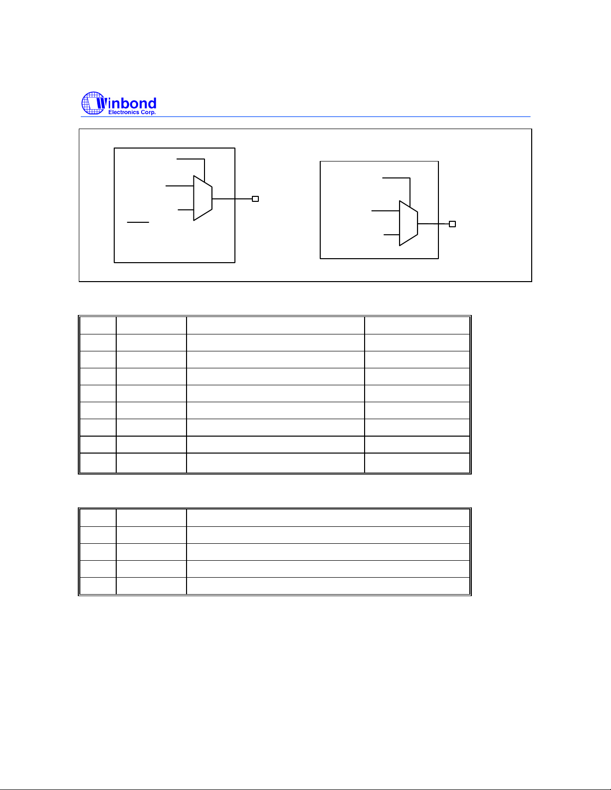
P2mSF
P2.m latch
SDACn
m n
4 10
5 11
6 12
7 13
0
P2.m/SDACn
1
*CONTREG5: Control register5.
BIT NAME FUNCTION NOTE
0
1
P23SF
P2.3 latch
STP output
0
1
W78E354
P2.3/STP
2
3
4
5 HDSEL HCLAMP Source SELect
6 DPARAINT Enable parabola with dummy Sync.
7
* STATUS: Status register.
BIT NAME FUNCTION
0 HP Hsync polarity. 0: Positive, 1: Negative.
1 VP Vsync polarity. 0: Positive, 1: Negative.
2 NOH Set by hardware if no Hsync.
3 NOV Set by hardware if no Vsync.
Publication Release Date: April 1997
- 19 - Revision A1
Page 20
W78E354
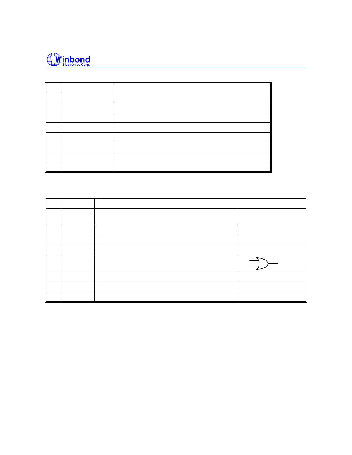
* INTMSK: Interrupt mask register.
BIT NAME FUNCTION
0 DSCLINTmsk Set/clear to enable/disable DSCLINT interrupt.
1 ADCINTmsk Set/clear to enable/disable ADCINT interrupt.
2 TIMEOUTmsk Set/clear to enable/disable TIMEOUT interrupt.
3 SOAINTmsk Set/clear to enable/disable SOAINT interrupt.
4 VEVENTmsk Set/clear to enable/disable VEVENT interrupt.
5 PARAINTmsk Set/clear to enable/disable PARAINT interrupt.
6 DDC1INTmsk Set/clear to enable/disable DDC1INT interrupt.
7
Note: A '1' in any bit of the INTMSK register enables the corresponding interrupt flag in INTVECT to be set by hardware when
the interrupt source generates an interrupt.
* INTVECT: Interrupt vector register.
BIT NAME FUNCTION NOTE
0 DSCLINT Set by hardware when DSCL is toggled from High to
See Section E.6.
Low and kept Low for at least 12/Fosc sec.
1 ADCINT Set by hardware when ADC conversion is completed.
2 TIMEOUT Set by hardware when Autoload timer timeout.
3 SOAINT Set by hardware when SOA is High.
4 VEVENT Set by hardware when Vsync or Vertical frequency
counter timeout.
5 PARAINT For parabola interrupt generator (set by hardware).
6 DDC1INT For DDC1 of DDC port (set by hardware).
See Section E.10.
See Section E.8.
See Section E.12.g.
VSEP
NOV
See Section E.9.
See Section E.6.
7
Note: To clear the interrupt flag, write a '1' (not '0') to the corresponding bit in INTVECT register.
* PARAL: Parabola interrupt generator register, low byte.
* PARAH: Parabola interrupt generator register, high byte.
* AUTOLOAD: 8-bit Auto-reload timer register. (See Section H.)
* DHREG: Dummy Hsync frequency generator register. (See Section L.e.)
* DVREG: Dummy Vsync frequency generator register. (See Section L.e.)
* DDC1: DDC port's DDC1 data buffer.
* DDAC0−DDAC2: 8-bit PWM dynamic DAC register. (See Section K.)
* BDDAC (8 bits)+DBRM (4 bits): 12-bit PWM/BRM dynamic DAC register. (See Section K.)
VEVENT
* SDAC0−SDAC13: 8 bits, 8-bit PWM static DAC register. (See Section K.)
* BSDAC0 (8 bits)+SBRM0 (4 bits): 12-bit PWM/BRM static DAC register. (See Section K.)
- 20 -
Page 21

W78E354
* BSDAC1 (8 bits)+SBRM1 (4 bits): 12-bit PWM/BRM static DAC register. (See Section K.)
* WDTCLR: Watchdog-timer-clear register, no specific hardware but an address. Writing any value to
WDTCLR will clear the watchdog timer.
* ADC: Result of the A-to-D conversion.
* HFCOUNTL: Horizontal frequency counter register, low byte. (See Section L.d.)
* HFCOUNTH: Horizontal frequency counter register, high byte. (See Section L.d.)
* VFCOUNTL: Vertical frequency counter register, low byte. (See Section L.d.)
* VFCOUNTH: Vertical frequency counter register, high byte. (See Section L.d.)
* PORT4: Latch outputs (output only).
* SOAREG: Safe-Operation-Area register. (See Section L.g.)
* SOACLR: Safe-Operation-Area Clear register, no specific hardware but an address. Writing
anyvalue to SOACLR will clear the SOA output (P1.5).
* S1CON: Serial Port 1 Control Register.
* S1STA: Serial Port 1 Status Register.
* S1DAT: Serial Port 1 Data Register.
* S1ADR: Serial Port 1 Address Register.
B. 16K Bytes Flash Memory
Programming the Flash memory will be described in section F.
C. 256 Bytes of On-Chip Data Memory
This data memory is mapped to external locations 00H to FFH and can only be accessed by the
"MOVX @Ri" instruction. Since no external data can be accessed by this chip, there is no need for
the external memory read/write control signals (RD, WR) as the "MOVX @Ri" instruction can only
be executed internally.
D. SPI (Synchronous Peripheral Interface) and RS232 Port: Serial Port 0
P3.0(RXD) and P3.1(TXD) can be used as a SPI port (serial port mode 0 of standard 80C51) or a
RS232 port (mode 1, 2 or 3).
• The SPI port can be used to communicate to OSD chip, DAC ...
• An RS232 port can be used to talk to auto-alignment system, by using an 18.432 MHz crystal,
aximun baud rate is 19200 bpS.
E. DDC Port (support DDC1/2B/2B+, with two slave address registers)
• One DDC1 port to support DDC1
• One I2C port support DDC2B/2B+: Serial Port 1
An Interrupt is generated when DSCL has a transition from high to low and then remains low for 12
clock periods.
Publication Release Date: April 1997
- 21 - Revision A1
Page 22
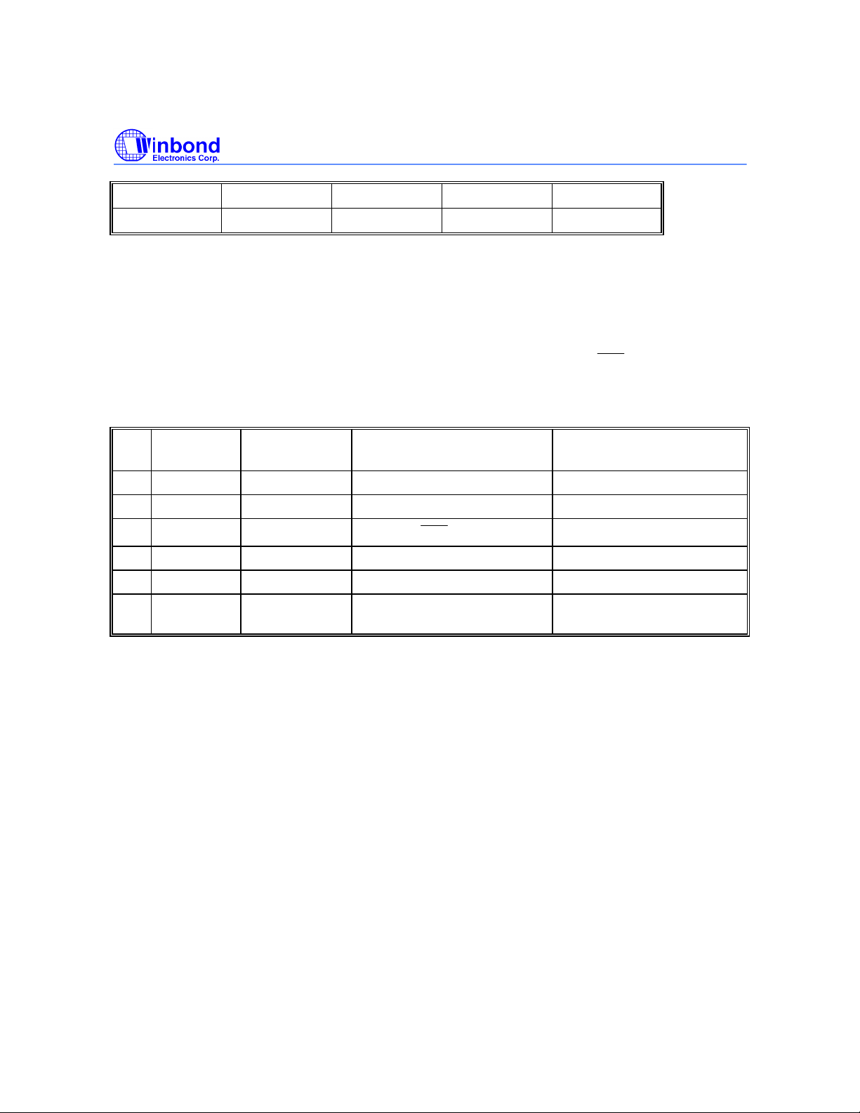
16 MHz 18.432 MHz 20 MHz 24 MHz
INT1
INT1
W78E354
DSCL Low
750 nS 651 nS 600 nS 499 nS
F. I2C Port: Serial Port 2
(S/W emulation).
G. Interrupts
The W78E354 has 6 interrupt sources. Five of them, with the exception of
0013H) are identical to those of the 8051 series. The remaining one (at vector address 002BH) is a
new addition. All the interrupt sources and the corresponding interrupt vector addresses for the
W78E354 are given in the following table:
SOURCE VECTOR
DDRESS
1 IE0 0003H Same as the 8051. Highest
2 TF0 000BH Same as the 8051.
3 *1 0013H
4 TF1 001BH Same as the 8051.
5 RI+TI 0023H Same as the 8051.
6 *2 002BH New addition.
Notes:
*1 = DSCLINT + ADCINT + TIMEOUT + SOAINT + VEVENT + PARAINT + DDC1INT.
*2 is the interrupt generated by the I2C in the DDC port.
Replaces
(like TF2 + EXF2 in the 8052)
DESCRIPTION PRIORITY WITHIN A LEVEL
of the 8051.
Lowest
(at vector address
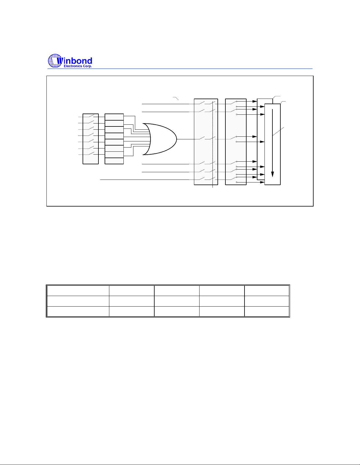
The interrupt at vector address 0013H is driven by another seven different sources. These are 1) a
High-to-low transition of the DSCL-pin, 2) the A/D converter, 3) the Auto-reload Timer, 4) the SOA
output, 5) Vsync, 6) the Parabola interrupt generator, and 7) DDC1 in the DDC port. The programmer
must read the INTVECT register to identify the interrupt request source. These seven sources can be
masked individually by setting the corresponding bit within the INTMSK register (Bit0..6). The newly
added interrupt at vector address 002BH is driven by the I2C circuit in the DDC port.
The interrupt enable control bits for the two interrupts at 0013H and 002BH are the bits IE.2 and IE.5
in the IE register, respectively. They can be disabled by clearing IE.7 (disable all interrupts). The
interrupt priority control bits are IP.2 and IP.5 in the IP register, respectively.
The following diagram illustrates the above description.
- 22 -
Page 23
W78E354
DSCLINT source
ADCINT source
TIMEOUT source
SOAINT source
VEVENT source
PARAINT source
DDC1INT source
2
I C in DDC port
INTMSK
Bit 0
Bit 1
Bit 2
Bit 3
Bit 4
Bit 5
Bit 6
INTVECT
DSCLINT
ADCINT
TIMEOUT
SOAINT
VEVENT
PARAINT
DDC1INT
Vector Address
IE0
TF0
OR
TF1
RI+TI
0003H
000BH
0013H
001BH
0023H
002BH
H. 8-bit Auto-reload Timer for Software Time Base
This is an 8-bit auto-reload timer, which generates a periodic interrupt to the CPU.
The time interval is programmable:
The minimun interval (unit) = 1/ (Fclock ÷ 1024),
the programmable interval = the minimun interval × (AUTOLOAD Reg. value +1),
IE
IE.0
IE.1
IE.2
IE.3
IE.4
IE.5
IE.7
IP
IP.0
IP.1
IP.2
IP.3
IP.4
IP.5
High Priority
Low Priority
Interrupt Polling
Sequence
the maximum interval = the minimun interval × 255.
16 MHz 18.432 MHz 20 MHz 24 MHz
Minimum Interval
64 µS 55 µS 51.2 µS 42.6 µS
Maximum Interval 16.3 mS 14.2 mS 13.1 mS 10.9 mS
I. Parabola interrupt generator
This is an 16-bit auto-reload timer, which generates a periodic interrupt to the CPU. The interrupt
period is programmable: the time base = 1/Fclock, the programmable interrupt period = the time base
× ([PARAH, PARAL] 16-bit Reg. value+1), the maximum period = the time base × 65535.
J. 6-bit ADC
One 6-bit Analog-to-Digital Converter.
SPEC.:
• ±1 LSB
Publication Release Date: April 1997
- 23 - Revision A1
Page 24
W78E354
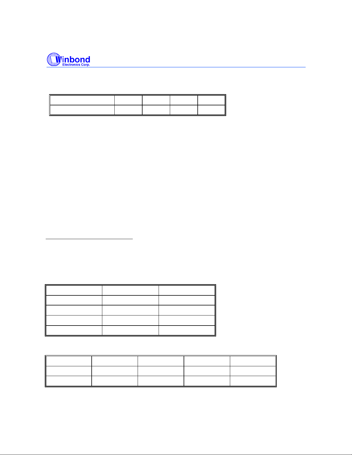
• Conversion time: <150 × 12/Fosc sec.
• 4 channels selected by an analog multiplexer
(ADCS1, ADCS0) (0, 0) (0, 1) (1, 0) (1, 1)
Selected Channel ADC0 ADC1 ADC2 ADC3
Set bits ADCS1 and ADCS2 in CONTREG1 to select one of the four analog input channels. The ADC
conversion is started by setting bit ADCSTRT in CONTREG1 using software. When the conversion is
comple, the ADCSTRT bit is cleared by hardware to stop the ADC operation. The ADCINT bit in
INTVECT is set by hardware at the same time.
K. PWM DACs
There are two/fourteen 12/8-bit PWM SDACs and one/three 12/8-bit PWM DDACs in this chip. All
the DAC output buffers have slew rate control to prevent the slew rate from being too large.
Additionally, their outputs are delay-controlled and divided into three groups with different delay times
as follows:
1. Delay about 5ns: BSDAC1, SDAC2, 5, 8, 11, DDAC1.
2. Delay about 10ns: SDAC0, 3, 6, 9, 12, DDAC2.
3. No delay: for the others.
Functional Descriptions:
a. 14 channels of 8-bit Static DAC
The Static DACs are used to generate DC voltages (0−5V). There are 14 registers each
corresponding to one 8-bit PWM 14 channel outputs. Unused PWM channels can be used as a
standard output pin, as these pins can supply 0V or 5V.
• The duty cycle of the PWM output = Register value ÷ 255
• The DC voltage after the low pass filter = VCC × duty cycle
REG. VALUE DUTY CYCLE DC VOLTAGE
0 0/255 0V
1 1/255
n n/255
255 255/255 +5V
• The PWM frequency FPWM = Fclock ÷ 255
16 MHz 18.432 MHz 20 MHz 24 MHz
FPWM 62.745 KHz 72.282 KHz 78.431 KHz 94.117 KHz
TPWM
15.94 µS 13.83 µS 12.75 µS 10.62 µS
1/255 × 5V
n/255 × 5V
- 24 -
Page 25
W78E354
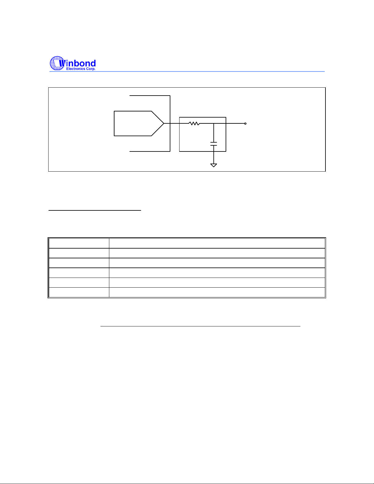
SDAC application circuit:
D1616
low pass filter
8/12bit resolution
SDAC
R
C
T = RC
Voutput = VCC × n/255, if T >> TPWM
b. 2 channels of 12-bit Static DAC
The two channel, 12-bit PWM outputs are composed of an 8-bit PWM and a 4-bit BRM (Bit Rate
Multiplier). The 4-bit BRM Reg. value decides which one is to be added one clock preiod in every 16
PWM outputs.
Output
BRM Reg. 4-bit data One clock period is incremented in the n-th output in every 16 PWM outputs.
0000 None
0001 n = 8
0010 n = 4, 12
0100 n = 2, 6, 10, 14
1000 n = 1, 3, 5, 7, 9, 11, 13, 15
Note: See the positions marked with an "*" in the following figure.
BRM BRM Cycle
Reg. value 0 1 2 3 4 5 6 7 8 9 10 11 12 13 14 15
0001 - - - - - - - - * - - - - - - 0010 - - - - * - - - - - - - * - - 0100 - - * - - - * - - - * - - - * 1000 - * - * - * - * - * - * - * - *
Example:
0000 - - - - - - - - - - - - - - - 0011 - - - - * - - - * - - - * - - 1111 - * * * * * * * * * * * * * * *
The 12-bit PWM frequency is the same as that of the 8-bit PWM output.
Publication Release Date: April 1997
- 25 - Revision A1
Page 26
W78E354
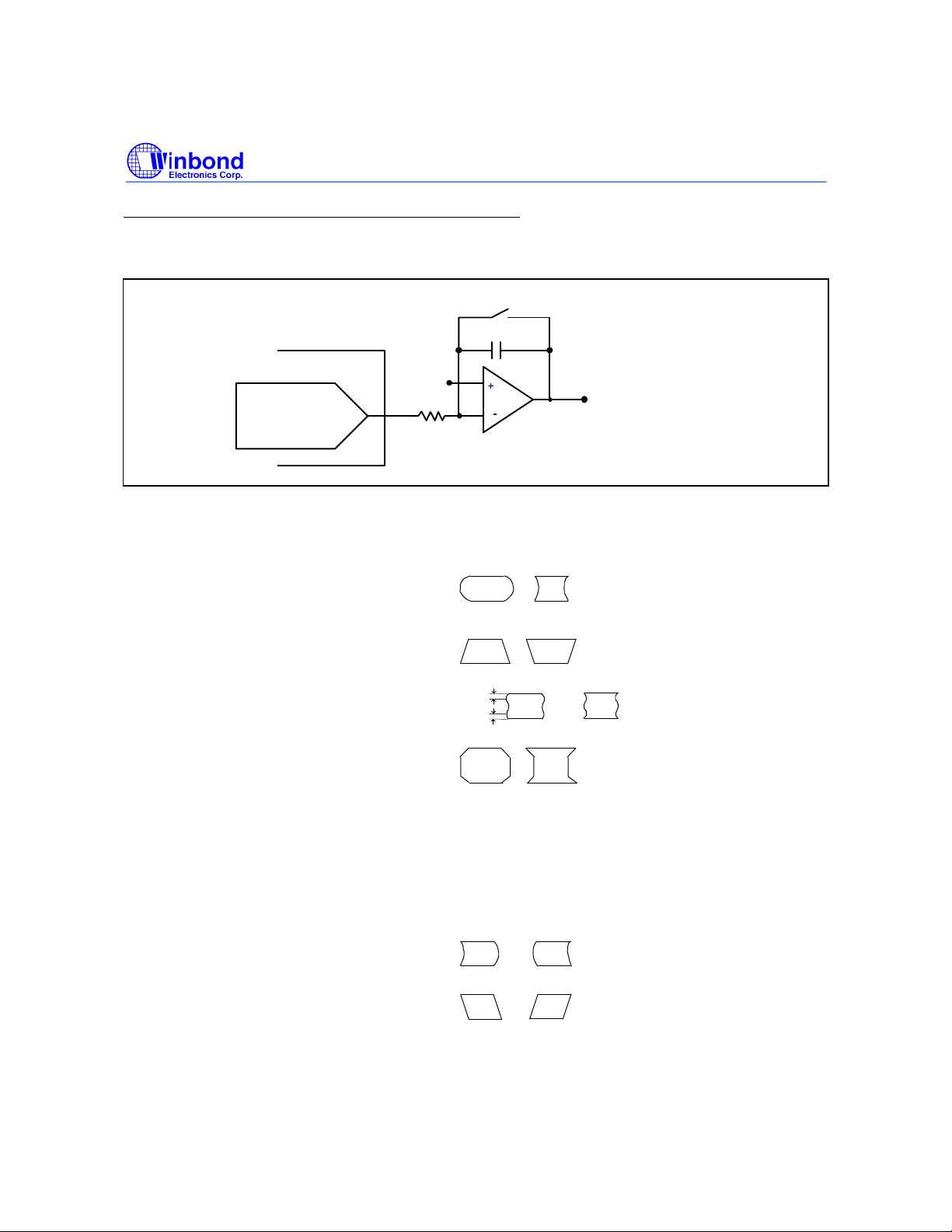
c. 1 channel of 12-bit & 3 channels of 8-bit Dynamic DAC
The Dynamic DACs are used to generate a parabola waveform for geometric compensation.
DDAC application circuit:
D1616
2.5V
8/12 bit resolution
DDAC
Geometry compensation parabola waveform:
DDAC0 can be used to compensate H size distortion:
Balanced/Unbalanced
Parabola
1. PinCushion Correction (amplitude)
(PCC amplitude)
2. Trapezoid (Keystone)
25%
3. CBOW (S-comp)
25%
4. PinCushion correction (corner)
(PCC corner)
The PCC amplitude can be compensated against V size adjustment automatically.
The Trapezoid can be compensated against V center adjustment automatically.
DDAC1 is used to compensate H center distortion:
1. Pin balance (Bow)
2. Key balance (Tilt)
Note: The unused dynamic DACs can be used as static DACs.
- 26 -
Page 27
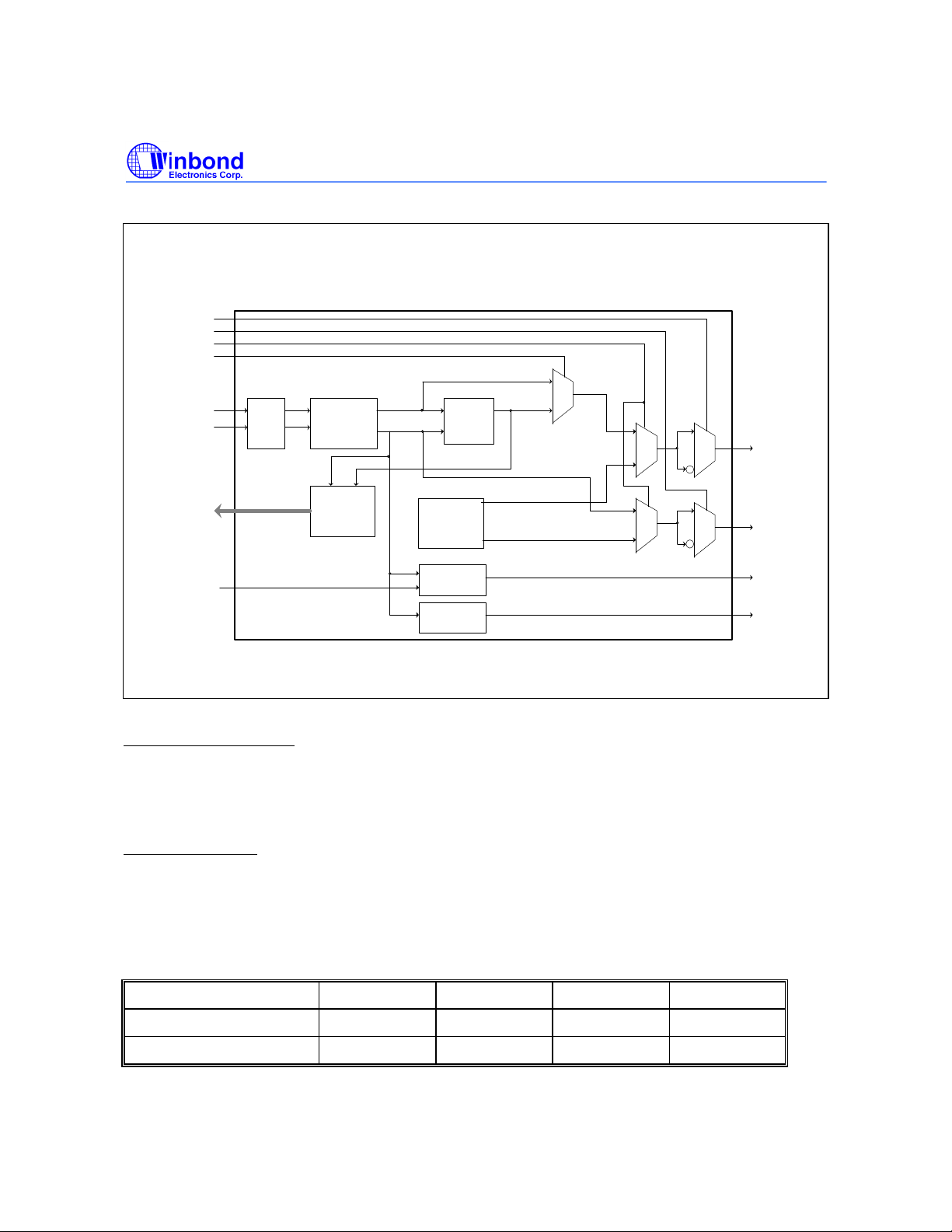
L. Sync Processor
VSPS
HSPS
DUMMYEN
ENVS
V
IN
IN
H
Digital
Filter
Polarity
Detect &
Restoration
Sync Processor Block Diagram
0
VREST
HREST
Vsync
Separator
VSEP
1
W78E354
0
1
0
1
OUT
V
VDUMMY
HDUMMY
0
1
0
1
OUT
H
H-Clamp
SOA
AD[7:0]
VDISHC
H/V
Frequency
Counter
H/V Dummy
Sync
Generator
H-Clamp
Generator
SOA
Generator
a. H/V Sync Digital Filter
Both Hsync and Vsync inputs have an internal digital filter to improve noise immunity. Any pulse that
is shorter than an internal clock period will be regarded as a glitch and will be ignored.
Ex: Tclock = 62 nS @16 MHz, any sync with pulse width less than 62 nS will be regarded as a glitch.
b. Polarity Detector
The H/V polarity is detected automatically and can be read from the STATUS register, the H/V input
signals are then polarity restored (become HREST/VREST) for internal processing and output to
HOUT/VOUT to drive the deflection circuit.
The maximun sync width to HIN pin is: (1/Fclock ) × 16384
The maximun sync width to VIN pin is: (1/Fclock ) × 16384
FCLOCK 16 MHz 18.432 MHz 20 MHz 24 MHz
Max. sync width for HIN
Max. sync width for VIN
1024 µS 888 µS 819 µS 681 µS
1024 µS 888 µS 819 µS 681 µS
- 27 - Revision A1
Publication Release Date: April 1997
Page 28
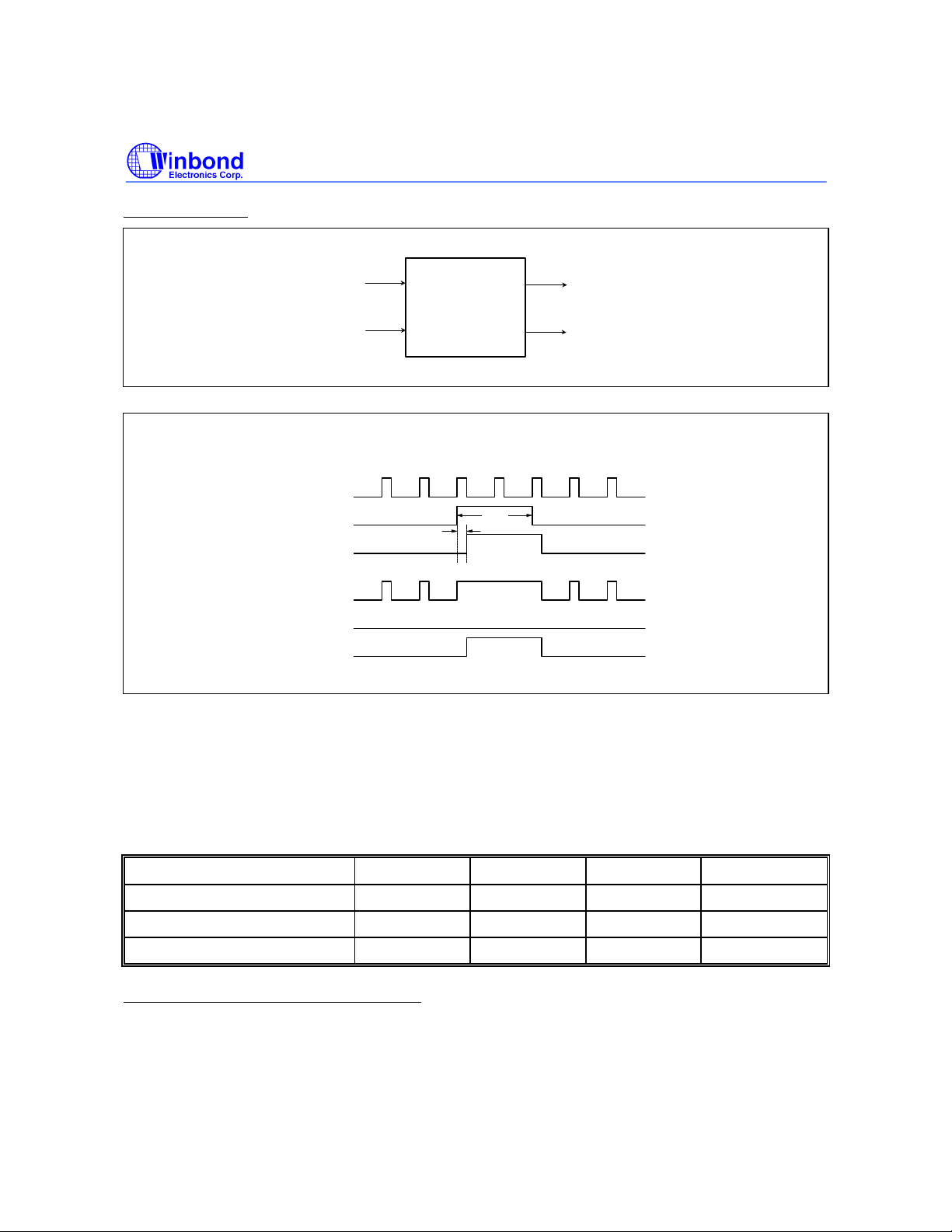
c. Sync Separator
Hsync/
Composite Sync
Vsync
Vsync Separator Output (VOUT = VSEP when DUMMYEN = 0, ENVS = 1):
IN
H
IN
V
OUT
V
IN
H
IN
V
Tdelay
OUT
H
OUT
V
Wvmin
To deflection circuit
W78E354
H (H+V)
IN
IN
V
OUT
V
The Vsync is separated from the composite sync automatically, without any software effort.
The limitation for the Vsync signal is:
the VIN pulse width must be larger than Wvmin = (1/Fclock) × 128.5, +/- 1/Fclock ÷ 2
VOUT is also delayed from the VIN signal by Tdelay = (1/Fclock) × 128.5, +/- 1/Fclock ÷ 2
(if ENVS bit is set to 1)
FCLOCK 16 MHz 18.432 MHz 20 MHz 24 MHz
1/Fclock 62.5 nS 54 nS 50 nS 41 nS
Min. Vsync Width (Wvmin) 8031 +/- 31 nS 6939 +/- 27 nS 6425 +/- 25 nS 5268 +/- 20 nS
VOUT Delay from VIN (Tdelay) 8031 +/- 31 nS 6939 +/- 27 nS 6425 +/- 25 nS 5268 +/- 20 nS
d. Horizontal & Vertical Frequency Counter
There are two 16-bit counters which can count H and V frequency automatically. When a VEVENT (V
frequency counter timeout) interrupt occurs, the MCU may read the count value (Hcount and Vcount)
from the counter registers (HFCOUNTH, HFCOUNTL, VFCOUNTH and VFCOUNTL) to calculate the
H and V frequency by the formulas listed below.
- 28 -
Page 29
W78E354
V frequency:
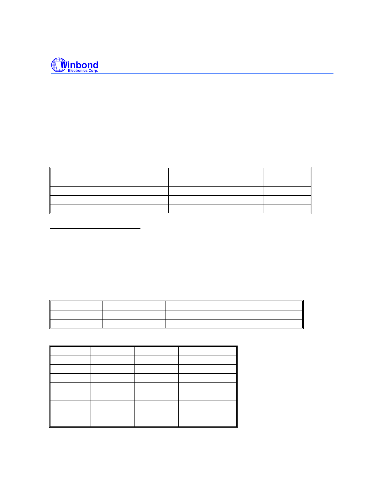
The resolution of V frequency counter: Vresol = (1/Fclock ) × 16.
The V frequency: Vfreq = 1/(Vcount × Vresol ).
The lowest V frequency can be detected: Fclock ÷ 1048576.
H frequency:
The resolution of H frequency counter: Hresol = (1/Fclock ) ÷ 8.
The H frequency: Hfreq = 1/(Hcount × Hresol ).
The lowest H frequency can be detected: Fclock ÷ 8192.
16 MHz 18.432 MHz 20 MHz 24 MHz
Vresol
The Lowest Vfreq 15 Hz 17.6 Hz 19 Hz 23 Hz
Hresol 7.8 nS 6.8 nS 6.3 nS 5.2 nS
The Lowest Hfreq 1.9 KHz 2.3 KHz 2.4 KHz 2.9 KHz
e. Dummy Frequency Generator
The Dummy H and V frequencies are generated for 1) factory burn-in and 2) displaying warning
messages if there is no input frequency.
There are two registers in the dummy sync generator:
DHREG: 4-bit register, determines the Dummy Hsync output frequency
DVREG: 8-bit register, determines the Dummy Vsync output frequency
1 µs
868 nS 800 nS 666 nS
Dummy Hsync frequency FdH = Fclock ÷ 32 ÷ (DHREG+1)
Dummy Vsync frequency FdV = FdH ÷ 8 ÷ (DVREG+1)
DUMMYEN HOUT VOUT
0 HREST VREST (if ENVS = 0), VSEP (if ENVS = 1)
1 HDUMMY VDUMMY
Ex. If System clock = 16 MHz
DHREG FdH DVREG FdV
15 31.25K 48 79.7 Hz
12 38.5K 59 80.2 Hz
10 45.5K 70 80.1 Hz
9 50K 77 80.1 Hz
7 62.5K 96 80.5 Hz
6 71K 109 80.7 Hz
5 82K 127 80.1 Hz
4 100K 155 80.1 Hz
- 29 - Revision A1
Publication Release Date: April 1997
Page 30

f. H-clamp Pulse Generator
If P14SF = 0, P1.4 is a general purpose I/O port.
If P14SF = 1, P1.4 is the H-clamp pulse output.
1. Leading edge / Trailing edge selectable
HCES = 0: select leading edge
HCES = 1: select trailing edge
Hsync
Hrest
Leading
Edge
Trailing
Edge
W78E354
2. Pulse width selectable
Hsync
H-cla mp
ouput
The pulse width is programmable: (1/Fclock) × Option, +/- 1/Fclock ÷ 2
(HCWS1, HCWS0)
OPTION 16 MHz 18.432 MHz 20 MHz 24 MHz
(0, 0) 4.5 281 +/- 31 nS 244 +/- 27 nS 225 +/- 25 nS 187 +/- 20 nS
(0, 1) 8.5 531 +/- 31 nS 461 +/- 27 nS 425 +/- 25 nS 353 +/- 20 nS
(1, 0) 16.5 1031 +/- 31 nS 896 +/- 27 nS 825 +/- 25 nS 686 +/- 20 nS
(1, 1) 32.5 2031 +/- 31 nS 1764 +/- 27 nS 1625 +/- 25 nS 1352 +/- 20 nS
g. SOA output
If P15SF = 0, P1.5 is a general purpose I/O port.
If P15SF = 1, P1.5 is the SOA output.
- 30 -
Page 31
W78E354
Purpose:
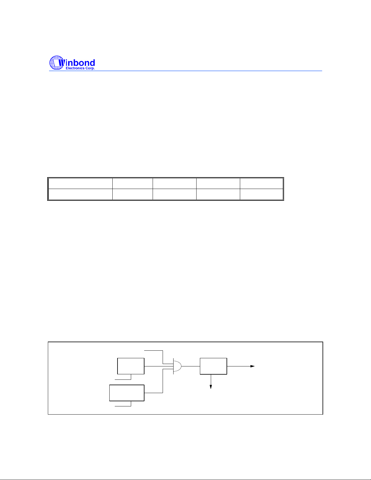
To protect the HOT (Horizontal Oscillating Transistor) and other critical circuitry by making a quick
response when the Hsync frequency drops below the preset boundary frequency.
Operation:
When the Hsync frequency is lower than the boundary frequency for three consecutive cycles or
stopped for a certain period, the SOA pin (P1.5) will change to a "high" state (for the extenal
protection circuit to function). Writing any value to the SOACLR register will release the SOA pin.
To set the boundary frequency, one can write some formula:value to the SOAREG register according
to the SOAREG value = 2M ÷ boundary frequency
Ex: If 50 KHz is considered the boundary frequency, then SOAREG = 2M ÷ 50K = 40.
No Hsync response time = 2048 × (1/Fclock ).
16 MHz 18.432 MHz 20 MHz 24 MHz
No H response time
128 µS 110 µS 102 µS 85 µS
M. Power Supervisor, Watchdog Timer and Reset Circuitry
The reset signals come from the following three sources:
1. External reset input (active low)
2. Power low detect
3. Hardware Watchdog Timer
The power-low detection circuit generates a reset signal once the VCC voltage falls below 3.8V. This
reset signal is released a short time after VCC has increased above 4.3V. This function can be
enabled or disabled by a code option.
The purpose of a watchdog timer is to reset the CPU if it enters erroneous processor states (possibly
caused by electrical noise or RFI) within a reasonable period of time. The watchdog timer clock
source comes from the internal system clock and can be enabled or disabled by a code option. When
enabled, the watchdog circuitry will generate a system reset if the user program fails to reload the
watchdog timer (by writing any value to the WDTCLR register) within a specified length of time known
as the "watchdog interval". The watchdog interval has four code options: 219/fosc, 221/fosc, 223/fosc
and 224/fosc sec.
The block diagram of the reset circuitry is shown as follows:
External Reset
EnWDT_Bit
Watchdog
Timer
EN
CPU
POR
XRESET
Reset the other
function blocks
EnSVS_Bit
Power-low
Detect Circuit
EN
Reset all DACs
Publication Release Date: April 1997
- 31 - Revision A1
Page 32
W78E354
FLASH CELL DESCRIPTION
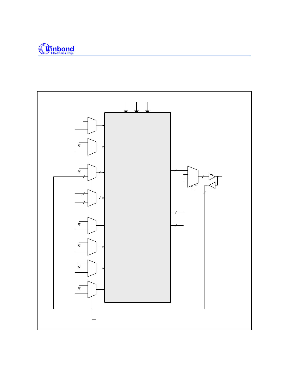
A. Flash ROM Interface
The following diagram shows the Flash cell block control interface. A<0:14> are the address bus
inputs and Dout<0:7> are the data bus outputs of the Flash ROM.
VPP VDDVSS
OSCEN
(normally "0")
/CE
(PAD)
/OE
(PAD)
PC
A<0:14>
(PAD)
A9CTRL
(PAD)
A13CTRL
(PAD)
0
1
s
/CE
Flash ROM (16KB)
0
8
15
/OE
Din<0:7>
A<0:14>
A9HV
Dout<0:7>
OPTION<0:7>
ROM-MAP<0:7>
8
8
MUX
8
8
8
D<0:7>
(PAD)
1
s
0
8
1
s
15
0
15
1
s
0
1
s
0
1
A13HV
s
0
A14CTRL
(PAD)
1
A14HV
s
0
OECTRL
(PAD)
* A14 = 0 at normal operation all the time.
1
OECTRL
s
Select signal will be decided by
/RESET, /PROG, A9CTRL, A13CTRL, A14CTRL and OECTRL.
Flash ROM Block Diagram
- 32 -
Page 33
W78E354
VPP is the high voltage input while in Flash Mode. A<0:14> is the address bus of the Flash cell while
in Flash Mode. Dout<0:7> is the data bus output of the Flash cell and Din<0:7> is the data bus input
while the chip is in Flash mode. The A9CTRL, A13CTRL, A14CTRL and OECTRL signals are used
to select the Flash Mode. The OE and CE signals are the control strobe signals for Flash Mode
operation. These signals are operational only in Flash Mode and appear as inputs/outputs via the
external pins with a "Test Name" as listed in the Pin Description in Sec. D.
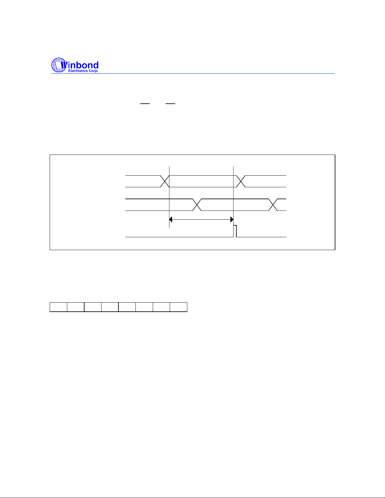
During normal operation, the critical timing parameter is the Flash data access time. When operating
at 24 MHz, the Flash cell requires 150 nS after an address out until the data is valid, as shown below.
Timing for Flash ROM Data Access
ROM
Address
A<0:14>
0000 0001 0002
ROM
Data
Dout<0:7>
Sample
Clock
Max. 150 nS for 24 MHz
#AAH
B. Option Setting Bits
The Option setting bits are used to set user-selectable options. These bits are programmed in the
same way as the 16K byte Flash ROM except for the address A<14:0> which is 7FFFH.
MSB LSB
B4 B3 B2 B1
Note: Default value is 1 for each bit.
• B1: EnWDT_Bit. (1: Disable, 0:Enable)
This bit is used to enable/disable the Watchdog Timer operation.
• (B3, B2): WatchDog Timer period set.
These two bits are used to set the time period of the Watchdog timer.
(0, 0): 219/fosc sec.
(0, 1): 221/fosc sec.
(1, 0): 223/fosc sec.
(1, 1): 224/fosc sec.
Where fosc is the crystal frequency.
• B4: EnSVS_Bit. (1: Disable, 0:Enable)
This bit is used to enable/disable the Power-low-detection function.
- 33 - Revision A1
Publication Release Date: April 1997
Page 34
W78E354
C. ROM-MAP Bits
In order to increase the functionality of the 16K byte Flash ROM, the Flash ROM is divided into 4
blocks. If some blocks contain bad Flash cells but the other blocks are good, the 16KB Flash can be
treated as either 8KB or 4KB, and the W78E354 downgraded to either the W78E352 or the
W78E351.
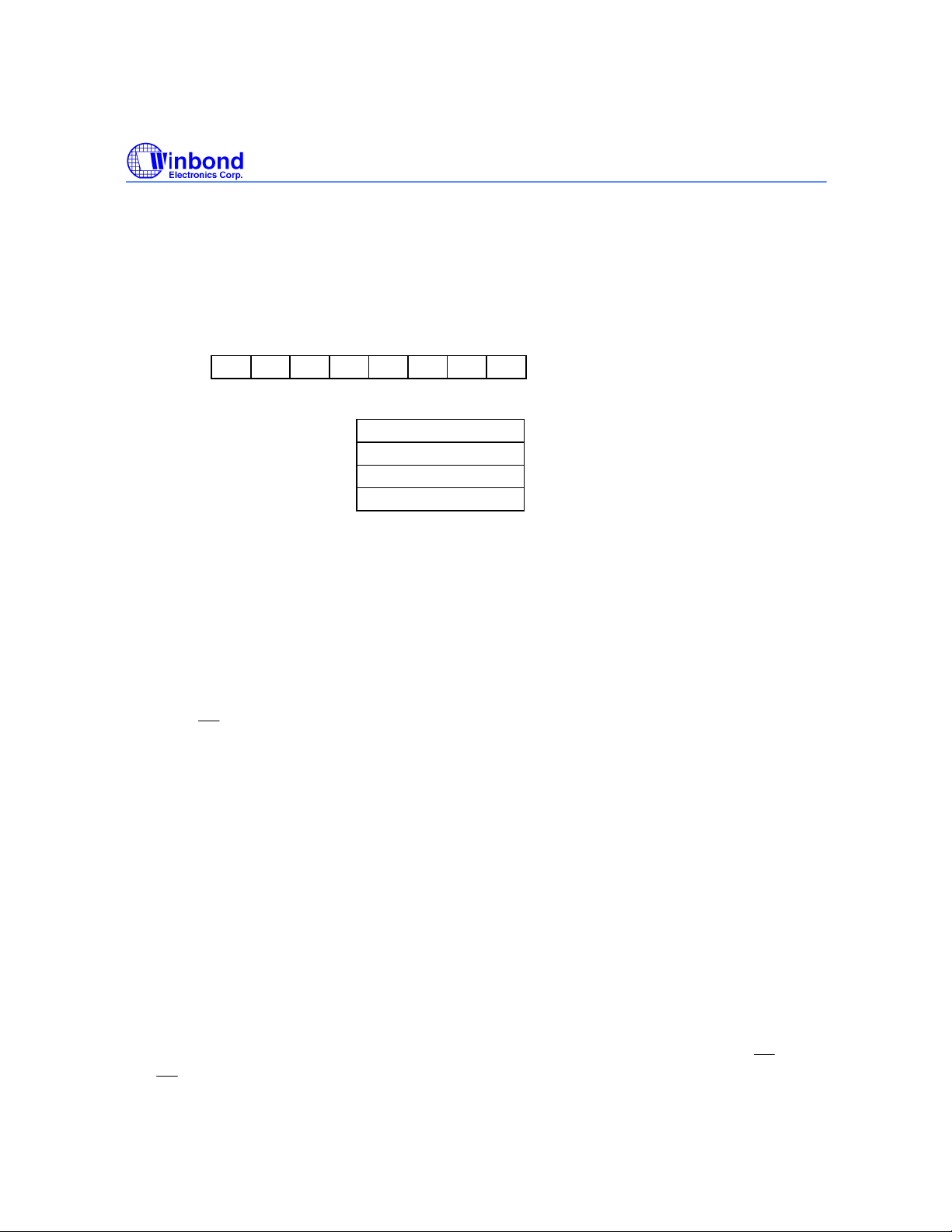
Four ROM-MAP bits are used to indicate the availability of the 16K bytes of Flash ROM after testing.
MSB LSB
ROM-MAP B3 B2 B1 B0
16K bytes Flash ROM
Set B0 = 1 if block 0 is available. Block 0, 4K bytes
Set B1 = 1 if block 1 is available. Block 1, 4K bytes
Set B2 = 1 if block 2 is available. Block 2, 4K bytes
Set B3 = 1 if block 3 is available. Block 3, 4K bytes
Note: Only one/two/four of the four bits can be set to indicate whether 4K/8K/16K are usable.
FLASH/TEST MODE
A. Flash Modes
1. Read
This mode is supported for customer code verification. The data will be invalid if the Lock bit is set
low.
2. Output Disable
When the OE is set high, no data outputs appear on D7..D0.
3. Standby
This condition disables the DC path from the Flash cell to reduce power consumption.
4. Program
This mode is used to program the Flash cell and option bits. It is the only way to change data from "1"
to "0".
5. Program Verify
All the programming data must be checked after program or mass program operations. This operation
should be performed after each byte is programmed to ensure a substantial program margin.
6. Erase
An erase operation is the only way to change data from "0" to "1".
7. Erase Verify
After an erase operation, all of the bytes in the chip must be verified to check whether they have been
successfully erased to 1 or not. The erase verify operation automatically ensures a substantial erase
margin. This operation will be implemented after the erase operation if VPP = VEP (14.5V), CE is high
and OE is low.
- 34 -
Page 35

W78E354
PSEN
8. Proram/Erase Inhibit
This operation allows parallel erasing or programming of multiple chips with different data.
9. Mass Program
In order to increase the throughput of testing, this operation programs 256 bytes with the same data
simultaneously. Note that 256 program verify operations must follow each mass program operation.
All the timings for this operation are the same as those of the byte program operation except that the
/CE program pulse width is 125µS. In addition, this operation is also used for cell reliability analysis
by stressing the source line.
10. Read Company ID and Device ID
These two modes are especially useful in EPROM WRITERs, which can read the silicon identification
to set the appropriate erase or program algorithm to match the device being erased or programmed.
11. VT
This operation is used for cell performance analysis. By connecting 2V to the D7..D0 pins, the cell
currents can be measured for each location within the chip by specifying its appropriate address.
12. Read ROM-map Bits
This operation is used to verify the ROM-MAP bits which were programmed previously. Its action is
the same as an EEPROM read operation.
13. Fuse ROM-map Bits
The ROM-MAP bits can be fused by this operation only. Its action is the same as an EEPROM
program operation.
14. Erase ROM-map Bits
The ROM-MAP bits can be erased by this operation only. Its action is the same as an EEPROM erase
operation.
15. CKBD & /CKBD Mass Program
These two operations are used to mass program the Flash cells in such a way that the state of any bit
is different from those of its neighboring bits.
16. Read Disturb
B. Test Mode
*RAM-test Mode
This mode is used to verify the function of the internal 512 bytes of RAM by a write-in and then readout operation.
*Functional Test Mode
If the EA (TestCLK) pin is pulled low when the chip is being reset and remains low for at least 24
clock periods after the reset, the CPU will execute from the external program memory (maximum
program size is 2K bytes). This feature may be used to test the chip's functions via an external
program. It should be noted that this mode is like the normal operation except that the CPU executes
from external program memory and that some different pins are used in place of A10−A0, D7−D0 and
instead of their original functions.
Publication Release Date: April 1997
- 35 - Revision A1
Page 36
W78E354
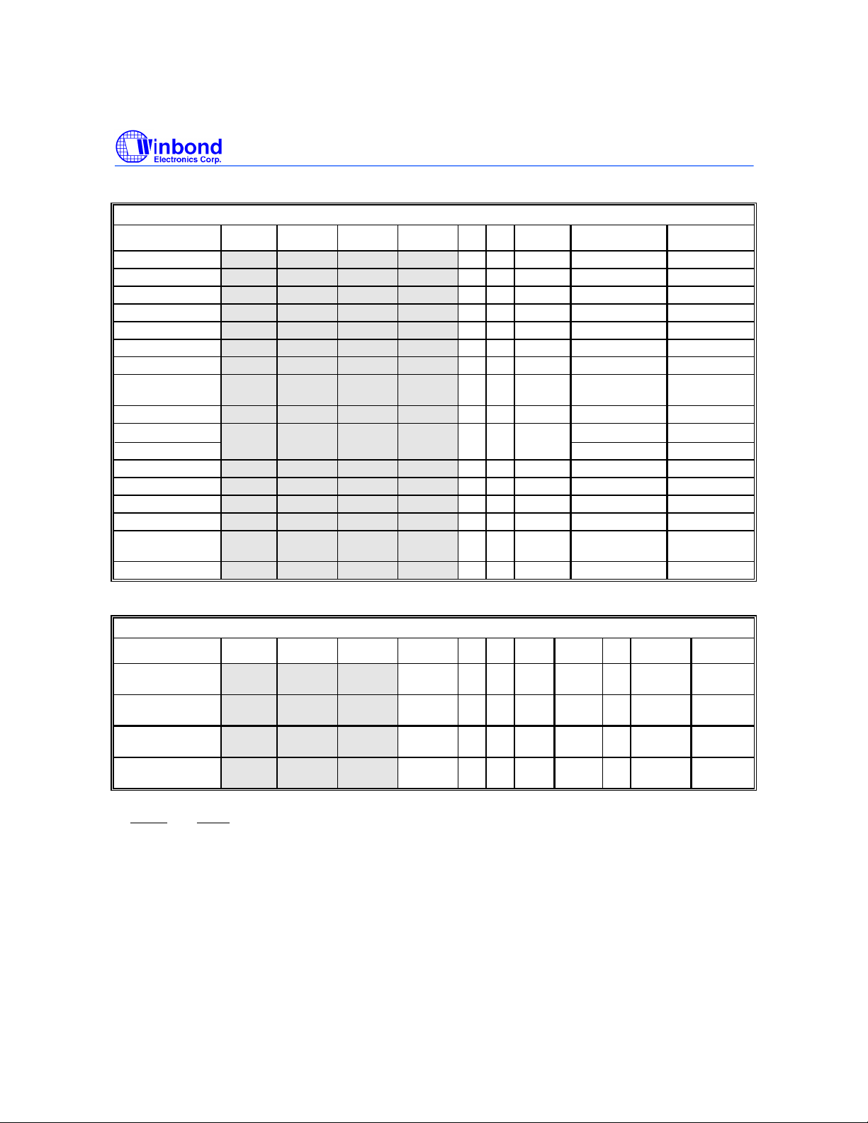
Flash/RAM-test Mode Configuration Table.
CONFIGURATION
Flash Modes A9CTRL A13CTRL A14CTRL OECTRL /CE /OE VPP A14..A0 D7..D0
Read 0 0 0 0 0 0 1 Address Data Out
Output Disable 0 0 0 0 0 1 1 X High-Z
Standby 0 0 0 0 1 X 1 X High-Z
Program 0 0 0 0 0 1 VCP Address Data In
Program Verify 0 0 0 0 1 0 VCP Address Data Out
[*3]
Erase
Erase Verify 1 0 0 0 1 0 VEP Address Data Out
Program/Erase
Inhibit
Mass Program 0 0 1 0 0 1 VCP X Data In
Read Company ID
Read Device ID
VT 0 0 0 1 0 1 1 Address Cell Current
Read ROM-MAP 0 1 0 0 0 0 1 7FFFh Data Out
Fuse ROM-MAP 0 1 0 0 0 1 VCP 7FFFh Data In
Erase ROM-MAP 1 1 0 0 0 1 VEP X Data In (FFh)
CKBD & /CKBD
Mass Program
Read Disturb 1 1 1 0 0 0 1 Address Data Out
1 0 0 0 0 1 VEP A0 = 0, others: X Data In (FFh)
0 0 0 0 1 1 VCP/VEP X X
1 0 0 0 0 0 1
1 0 1 0 0 1 VCP A6, A0
A0 = 0, others: X
A0 = 1, others: X
[*4]
Data Out (DAh)
Data Out (64h)
Data In (00h)
CONFIGURATION
RAM-test Modes A9CTRL A13CTRL A14CTRL OECTRL /CE /OE VPP A14..A9 A8 A7..A0 D7..D0
8032's 256 bytes of
RAM-write
8032's 256 bytes of
RAM-read
Data Memory by
MOVX-write
Data Memory by
MOVX-read
Notes:
1: RESET and PROG must be kept low for all the above modes.
2: "X" means "Don't care" but not floating. VCP = 12.5V, VEP = 14.5V, "1" stands for VDD and "0" for VSS.
*3: The Erase operation erases all the 16K bytes of Flash cell but not the ROM-MAP cell.
*4: A0/A6 decides whether the bit-line/word-line is even or odd.
0 1 1 X 0 1 X X 0 Address Data In
0 1 1 X 1 0 X X 0 Address Data Out
0 1 1 X 0 1 X X 1 Address Data In
0 1 1 X 1 0 X X 1 Address Data Out
- 36 -
Page 37
W78E354
For CKBD, (A6, A0) = (0, 0) and then (1, 1); for /CKBD, (A6, A0) = (1, 0) and then (0, 1).
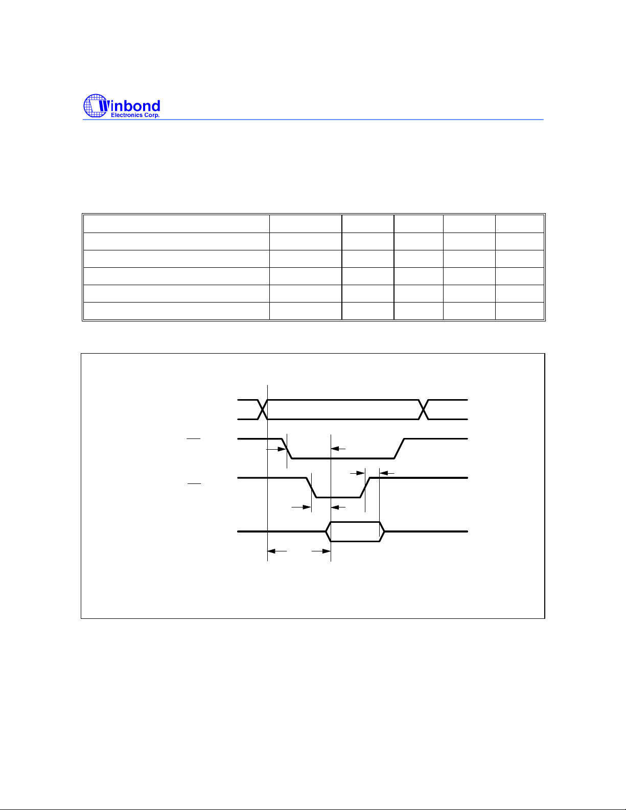
G.3 Flash Mode Timing Waveforms
*Read Operation
(including EEPROM, Company ID, Device ID, Option bits and ROM-MAP bits Read)
PARAMETER SYMBOL MIN. TYP. MAX. UNIT
Address Access Time TACC - - 150 nS
Chip Enable Access Time TCE - - 150 nS
Output Enable Access Time TOE - - 150 nS
Output Data Hold Time TODH 0 - - nS
Output Data Float Time TODF - - 100 nS
Read Waveform
V
(A14..A0)
OE
CE
D7..D0
Note: Please pay attention to the relation between /CE's and /OE's waveforms.
IH
V
IL
V
IH
V
IL
V
IH
V
IL
V
IH
V
IL
Valid Address
T
OE
T
CE
T
ACC
Data
T
ODH/ODF
Publication Release Date: April 1997
- 37 - Revision A1
Page 38
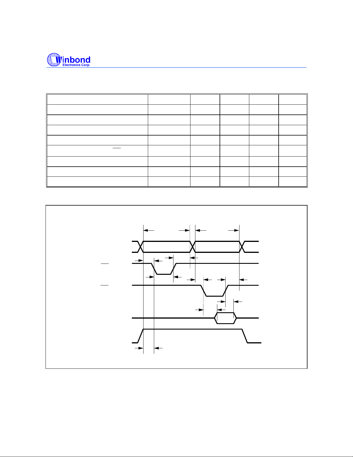
*Erase Operation
(including EEPROM&Option bits and ROM-MAP bits Erase)
PARAMETER SYMBOL MIN. TYP. MAX. UNIT
W78E354
Vpp Setup Time TVPS 2.0 - Address Setup Time TAS 2.0 - Address Hold Time TAH1 2.0 - Erase Pulse Width TEPW - 1 5 mS
Output Data Valid after OE Low
TODV - - 150 nS
Address Hold Time TAH2 0 - Output Data Hold Time TODH 0 - - nS
Output Data Float Time TODF - - 100 nS
Erase Waveform
Erase
Verify
Address Stable
T
AS
T
AH2
ODH/ODF
T
A14..A0
CE
OE
V
V
V
V
V
VIL
Erase
IH
A0 = 0
IL
T
IH
IL
AS
T
IH
EPW
T
AH1
µS
µS
µS
µS
D7..D0
VPP
V
IH
V
IL
Vep
V
IH
T
ODV
D
OUT
T
VPS
- 38 -
Page 39
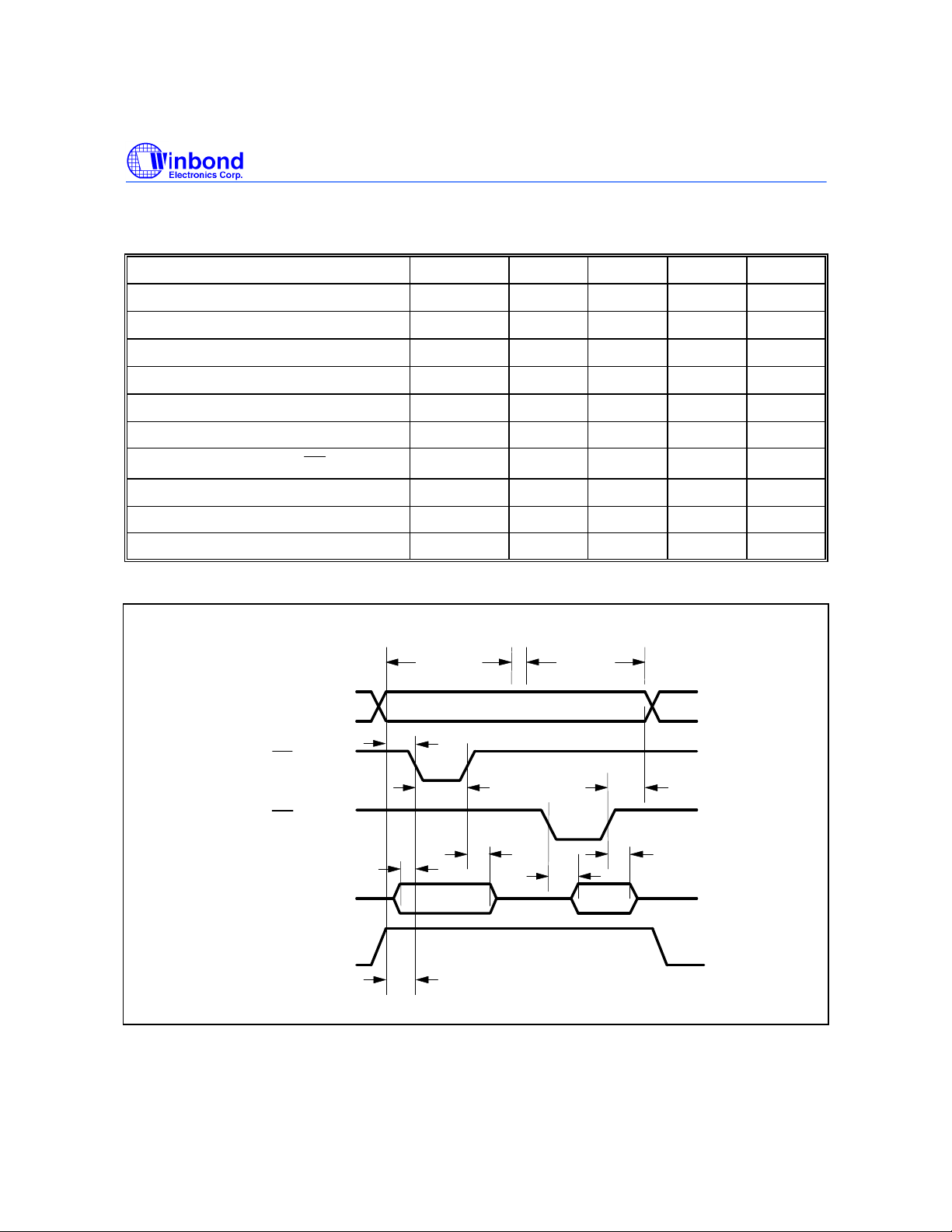
*Program & Mass Program Operation
(including EEPROM, Option bits and ROM-MAP bits Program, and Mass Program)
PARAMETER SYMBOL MIN. TYP. MAX. UNIT
W78E354
Vpp Setup Time TVPS 2.0 - Address Setup Time TAS 2.0 - Input Data Setup Time TIDS 2.0 - Input Data Hold Time TIDH 2.0 - Program Pulse Width TPPW - 100 200
Mass Program Pulse Width TMPPW - 500 1000 mS
Output Data Valid after OE Low
TODV - - 150 nS
Address Hold Time TAH 0 - Output Data Hold Time TODH 0 - - nS
Output Data Float Time TODF - - 100 nS
Program Waveform
Program
Verify
A14..A0
Program
V
IH
V
IL
V
IH
Address Stable
T
AS
CE
V
OE
D7..D0
VPP
V
V
V
V
Vcp
V
IL
IH
IL
IH
IL
IH
T
PPW
T
IDH
T
IDS
T
ODV
Data In
T
VPS
T
T
Data Out
AH
ODH/ODF
µS
µS
µS
µS
µS
µS
Publication Release Date: April 1997
- 39 - Revision A1
Page 40
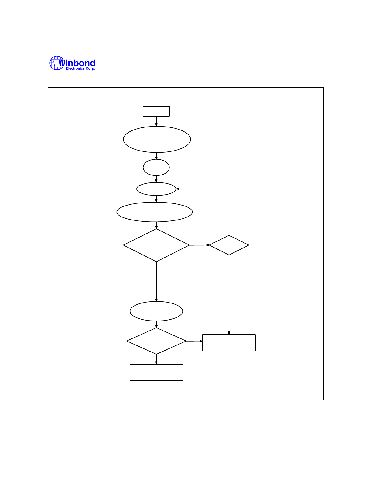
D.1 Smart Erase Algorithm
W78E354
Start
Vpp = 14.5V
Enter ERASE Mode
N = 0
Increment N
Erase one 1 mS pulse
Erase Verify
(Verify all bytes,
must be FFh)
PASS
Vpp = 5.0V
Enter READ Mode
Read Verify
(Blank check)
PASS
Erase Pass !
NO
FAIL
N = 10 ?
YES
FAIL
Erase Fail !
- 40 -
Page 41
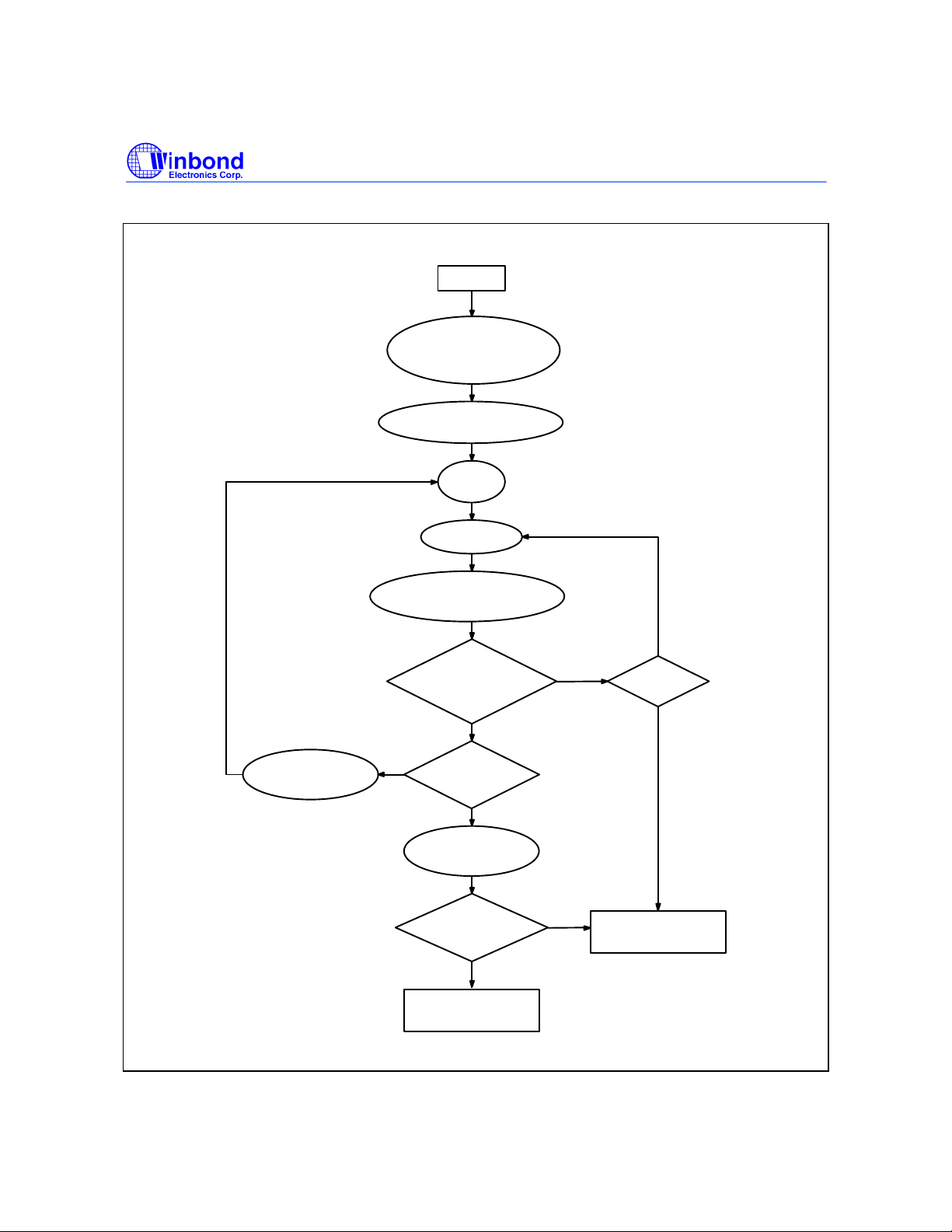
D.2 Smart Program Algorithm
W78E354
Start
Vpp = 12.5V
Enter PROGRAM Mode
Address = First Location
N = 0
Increment N
Increment Address
Program One 100 uS Pulse
Program Verify
(Verify one byte)
PASS
NO
Last Address ?
YES
Vpp = 5.0V
Enter Rdad Mode
Read Verify
(Verify all bytes)
PASS
Program Pass !
NO
FAIL
N = 10 ?
YES
FAIL
Program Fail !
Publication Release Date: April 1997
- 41 - Revision A1
Page 42
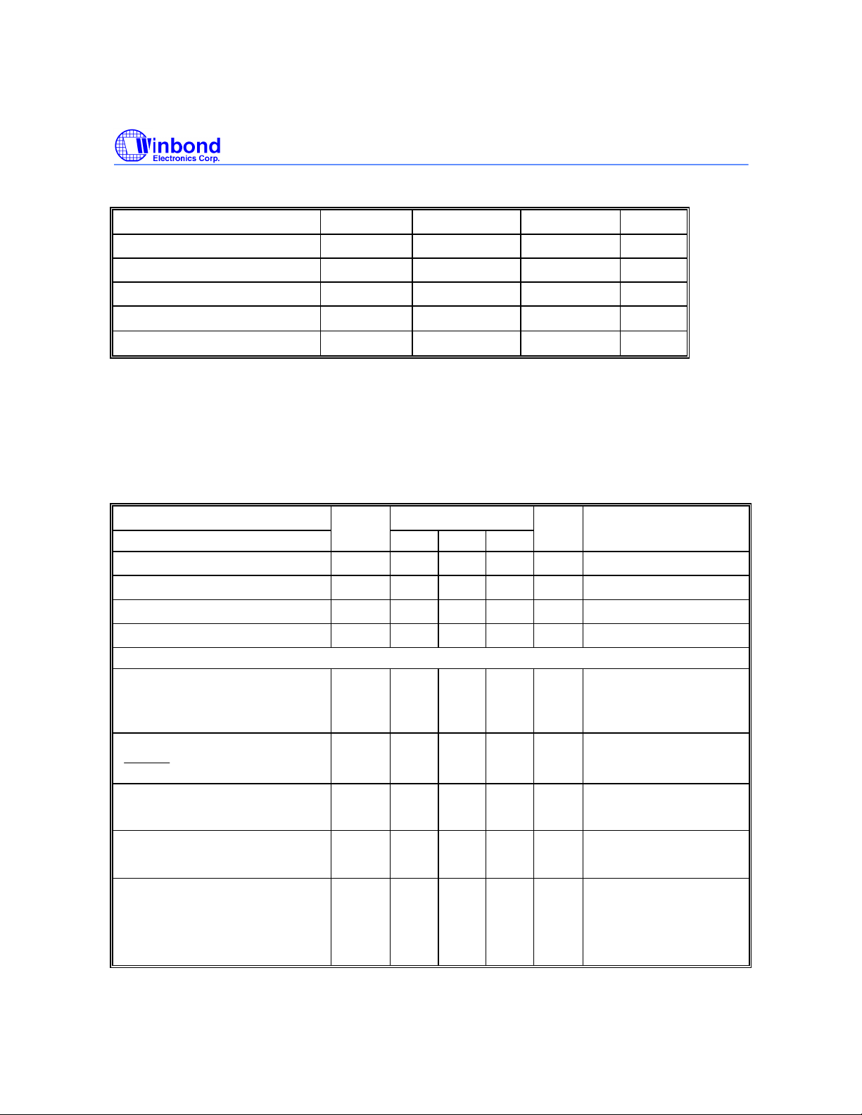
ABSOLUTE MAXIMUM RATINGS
RESET
PARAMETER SYMBOL MIN. MAX. UNIT
DC Power Supply VDD -0.3 +7.0 V
Input Voltage VIN VSS -0.3 VDD +0.3 V
Input Current II -100 +100 mA
W78E354
Operating Temperature TA 0 70
Storage Temperature TST -55 150
Note: Exposure to conditions beyond those listed under Absolute Maximum Ratings may adversely affect the life and reliability
of the device.
°C
°C
ELECTRICAL CHARACTERISTICS
Normal Operation D.C. Characteristics
(VDD & VAA)−VSS = 5V ±10%, TA = 25°C, Fosc = 20 MHz, unless otherwise specified.
PARAMETER SYM. SPECIFICATION UNIT TEST CONDITIONS
Min. Typ. Max.
Operating Voltage
Operating Current
Idle Current IIDLE
Power-down Current IPD
Logic 0 Input Current
P1, P2, P3 (except P1.0−P1.3,
P1.5)
Input Current
, TestCLK
(*1)
Input Current
HIN, VIN
(*2)
Input Leakage Current
P1.0−P1.3, ADC0−ADC3
Logical 1-to-0 Transition
Current
P1, P2, P3
(*3)
VDD 4.5 5 5.5 V
IDD - - 65 mA No load, VDD = 5.5V
- - 30 mA No load, VDD = 5.5V
- - 10
No load, VDD = 5.5V
µA
Inputs
IIN1
-75 - -10
µA
VDD = 5.5V
VIN = 0V
IIN2
-250 - -
µA
VDD = 5.5V
VIN = 0V
IIN3
- - +30
µA
VDD = 5.5V
VIN = VDD
ILK
-10 - +10
µA
VDD = 5.5V
0V < VIN < VDD
ITL
-650 - -
µA
VDD = 5.5V
VIN = 2.0V
(except P1.0−P1.3, P1.5)
- 42 -
Page 43
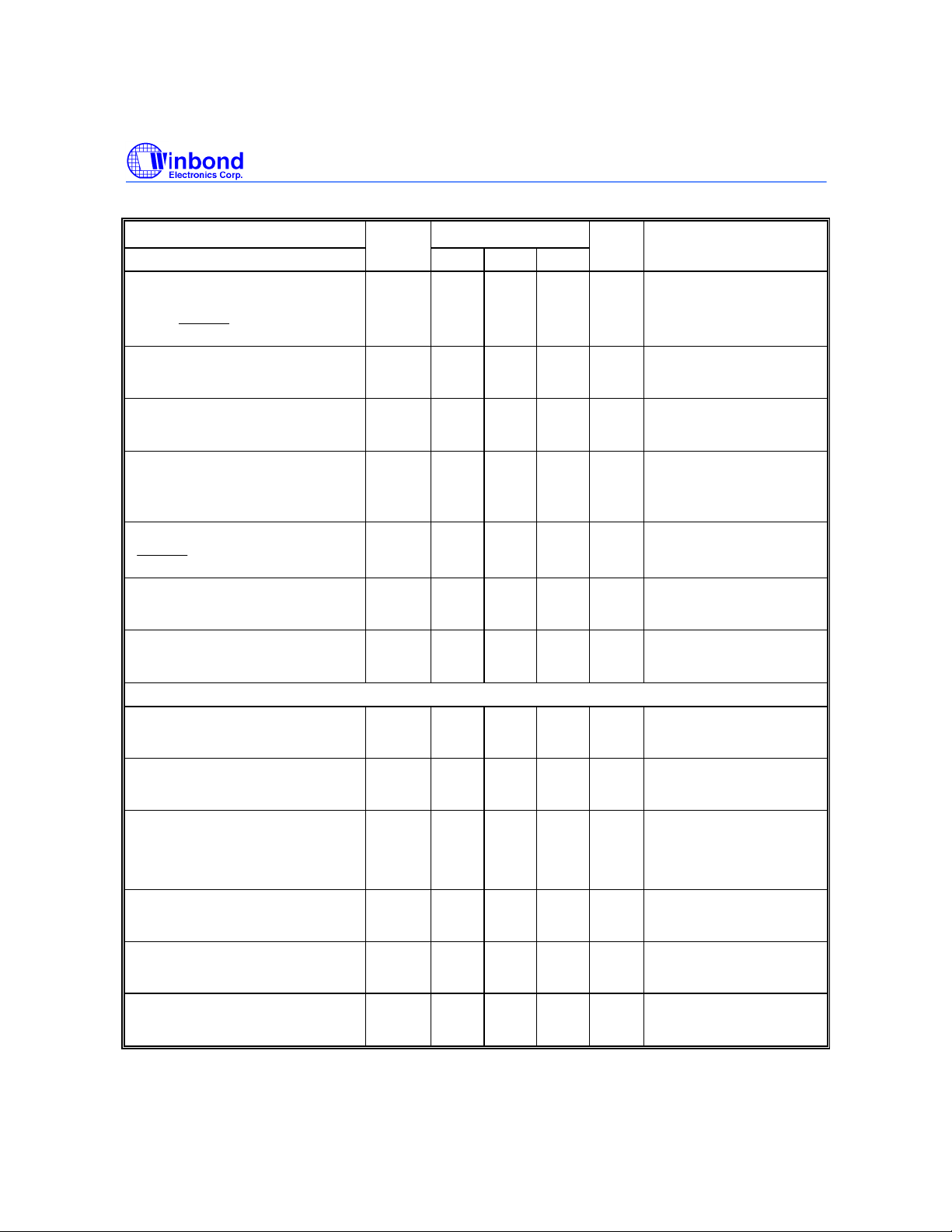
Normal Operation D.C. Characteristics, continued
RESET
RESET
PARAMETER SYM. SPECIFICATION UNIT TEST CONDITIONS
Input Low Voltage
(*4)
P1, P2, P3 (except P1.0−P1.3,
P1.5)
Input Low Voltage
(*4)
HIN, VIN
Input Low Voltage
(*4)
P1.0−P1.3
Input High Voltage
P1, P2, P3 (except P1.0−P1.3,
P1.5)
Input High Voltage
(*4)
, OSCIN
Input High Voltage
(*4)
HIN, VIN
Input High Voltage
(*4)
P1.0−P1.3
Output Low Voltage
P1.0, P1.1
Output Low Voltage
P1.2, P1.3
Output Low Voltage
P1.4, P1.5, P2.2−P2.7
VIL1
VIL2
VIL3
VIH1
VIH2
VIH3
VIH4
VOL1
VOL2
VOL3
Min. Typ. Max.
0 - 0.8 V VDD = 4.5V
0 - 0.8 V VDD = 4.5V
0 - 1.5 V VDD = 4.5V
2.4 - VDD
V VDD = 5.5V
+0.2
3.5 - VDD
V VDD = 5.5V
+0.2
2.4 - VDD
V VDD = 5.5V
+0.2
3.0 - VDD
V VDD = 5.5V
+0.2
Outputs
- - 0.4 V VDD = 4.5V
IOL = +2 mA
- - 0.4 V VDD = 4.5V
IOL = +6 mA
- - 0.45 V VDD = 4.5V
IOL = +4 mA
W78E354
SDAC0−13, HOUT, VOUT
Output Low Voltage
P2.0, P2.1
Output Low Voltage
P3, P4
Output Low Voltage
BSDAC0−1, DDAC0−2, BDDAC
VOL4
VOL5
VOL6
- - 0.5 V VDD = 4.5V
IOL = +15 mA
- - 0.45 V VDD = 4.5V
IOL = +2 mA
- - 0.45 V VDD = 4.5V
IOL = +8 mA
Publication Release Date: April 1997
- 43 - Revision A1
Page 44
Normal Operation D.C. Characteristics, continued
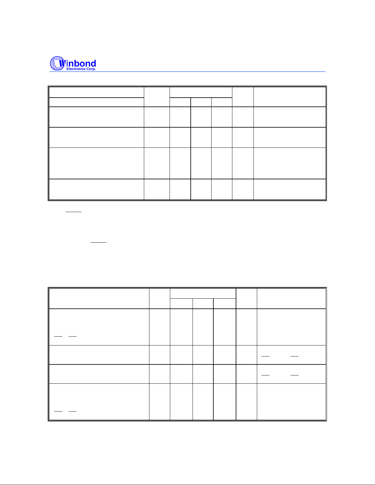
OE, CE
CE
CE
OE, CE
PARAMETER SYM. SPECIFICATION UNIT TEST CONDITIONS
Min. Typ. Max.
Output High Voltage
VOH1
P1.4, P2, P3
Output High Voltage
VOH2
P4
Output High Voltage
VOH3
P1.5, SDAC0−13, HOUT, VOUT
S.F. of P1.4 and P2.3−P2.7
Output High Voltage
(*5)
VOH4
BSDAC0−1, DDAC0−2, BDDAC
Notes:
*1. RESET and TestCLK have an internal pull-up resistor of about 30 KΩ.
*2. HIN and VIN have an internal pull-down resistor of about 200 KΩ.
*3. P1, P2 and P3 (except P1.0−P1.3 and P1.5) can source a transition current when they are being externally
driven from 1 to 0. The transition current reaches its maximum value when VIN is approximately 2V.
*4. P1.0−P1.3, RESET , HIN and VIN are Schmitt trigger inputs, and OSCIN is a CMOS input.
*5. While outputing a special function, the source current of P1.4 and P2.3−P2.7 is -4 mA.
2.4 - - V VDD = 4.5V
IOL = -100 µA
2.4 - - V
VDD = 4.5V
IOH = -2 mA
2.4 - - V
VDD =4.5V
IOH = -4 mA
2.4 - - V
VDD = 4.5V
IOH = -8 mA
W78E354
Flash Operation D.C. Characteristics
(VDD & VAA)−VSS = 5V ±10%, TA = 25°C, Fosc = 20 MHz, unless otherwise specified.
PARAMETER SYM. SPECIFICATION UNIT TEST CONDITIONS
MIN. TYP. MAX.
Input Current
IIN
-75 - +10
A0−A14, D0−D7, A9CTRL,
A13CTRL, A14CTRL, OECTRL,
VPP Erase Current (VPP = VEP) IEP
VPP Program Current (VPP = VCP) ICP
Input Low Voltage
VIL
- - +200
- - +200
0 - 0.8 V VDD = 4.5V
A0−A14, D0−D7, A9CTRL,
A13CTRL, A14CTRL, OECTRL,
VDD = 5.5V
µA
VIN = 0V or VDD
VDD = 5.5V
µA
VDD = 5.5V
µA
= VIL, CE = VIH
= VIL, CE = VIH
- 44 -
Page 45
Flash Operation D.C. Characteristics, continued
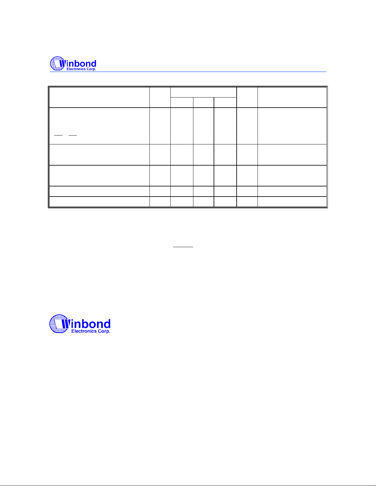
OE, CE
RESET
Note: All data and specifications are subject to change without notice.
PARAMETER SYM. SPECIFICATION UNIT TEST CONDITIONS
Input High Voltage
A0−A14, D0−D7, A9CTRL,
A13CTRL, A14CTRL, OECTRL,
VIH
MIN. TYP. MAX.
2.4 - VDD
+0.2
W78E354
V VDD = 5.5V
Output Low Voltage
VOL
D0−D7
Output High Voltage
VOH
D0−D7
VPP Erase Voltage VEP
VPP Program Voltage VCP
- - 0.45 V VDD = 4.5V
IOL = +2 mA
2.4 - - V VDD = 4.5V
IOH = -100 µA
14.25 14.5 14.75 V
12.25 12.5 12.75 V
TYPICAL APPLICATION
Please note:
While the chip is being powered on and the
same time, then the POR (Power-on Reset) will last until P1.5 or P3.2 is pulled High, whichever
occurs first.
pin is low, if P1.5 and P3.2 are kept low at the
Headquarters
No. 4, Creation Rd. III,
Science-Based Industrial Park,
Hsinchu, Taiwan
TEL: 886-3-5770066
FAX: 886-3-5792697
http://www.winbond.com.tw/
Voice & Fax-on-demand: 886-2-27197006
Taipei Office
11F, No. 115, Sec. 3, Min-Sheng East Rd.,
Taipei, Taiwan
TEL: 886-2-27190505
FAX: 886-2-27197502
Winbond Electronics (H.K.) Ltd.
Rm. 803, World Trade Square, Tower II,
123 Hoi Bun Rd., Kwun Tong,
Kowloon, Hong Kong
TEL: 852-27513100
FAX: 852-27552064
- 45 - Revision A1
Winbond Electronics North America Corp.
Winbond Memory Lab.
Winbond Microelectronics Corp.
Winbond Systems Lab.
2727 N. First Street, San Jose,
CA 95134, U.S.A.
TEL: 408-9436666
FAX: 408-5441798
Publication Release Date: April 1997
 Loading...